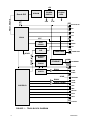
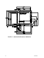
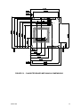
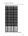
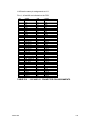
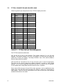
1
TP400 PC/104-PLUS
PC COMPATIBLE COMPUTER
TECHNICAL REFERENCE MANUAL
Revision B00
TRM-TP400 158004.B00
19 February 2001
CGP
(This page is intentionally left blank)
All information in this manual is believed to be accurate and reliable. However, no
responsibility is assumed by DSP Design Limited for its use. Since conditions of
product use are outside our control, we make no warranties express or implied in
relation thereto. We therefore cannot accept any liability in connection with any use
of this information. Nothing herein is to be taken as a license to operate under or a
recommendation to infringe any patents.
Whilst every effort has been made to ensure that this document is correct, errors can
occur. If you find any errors or omissions please let us know, so that we can put this
right.
All information contained in this manual is proprietary to DSP Design Limited and
cannot be reproduced without the consent of DSP Design Limited. The circuit design
and printed circuit board design is copyright of DSP Design Limited 2000.
DSP Design Limited
Tapton Park Innovation Centre
Brimington Road
Chesterfield S41 0TZ
United Kingdom
Tel
Fax
Email
Web:
+44 (0) 1246 545 910
+44 (0) 1246 545 911
[email protected]
www.dspdesign.com
(This page is intentionally left blank).
CONTENTS
1
INTRODUCTION ..................................................................................................1
1.1
OVERVIEW ....................................................................................................................................... 1
1.2
TP400 FEATURES............................................................................................................................ 2
1.3
PC/AT COMPATIBILITY.................................................................................................................... 3
1.4
PC/104-PLUS AS A PC EXPANSION BUS...................................................................................... 4
1.5
THE TP400 ARCHITECTURE .......................................................................................................... 4
1.6
GETTING STARTED QUICKLY ....................................................................................................... 7
1.6.1
TCDEVPLUS and TCDEV Development Systems .................................................................. 7
1.6.2
Using the TCDEVPLUS Development System ........................................................................ 8
1.6.3
Using the Rev D TCDEV Development System ....................................................................... 9
1.6.4
TCONN Connector Breakout Board .......................................................................................11
1.7
AVOIDING COMMON PROBLEMS................................................................................................12
2
PROCESSOR AND MEMORY...........................................................................13
2.1
2.2
2.3
2.4
2.5
PROCESSOR..................................................................................................................................13
CLOCK.............................................................................................................................................15
SDRAM ............................................................................................................................................16
FLASH MEMORY............................................................................................................................17
MEMORY ADDRESS MAP .............................................................................................................18
3
PERIPHERALS...................................................................................................19
3.1
I/O ADDRESS MAP.........................................................................................................................19
3.2
SUPER I/O CHIP .............................................................................................................................21
3.3
EXTRA UART ..................................................................................................................................21
3.4
SERIAL PORTS...............................................................................................................................21
3.4.1
Signals, Addressing and Interrupts .........................................................................................21
3.4.2
RS-485 Operation....................................................................................................................22
3.4.3
Disabling Serial Ports ..............................................................................................................23
3.4.4
Extended Modes......................................................................................................................23
3.4.5
Infra-Red Operation Modes.....................................................................................................23
3.5
PRINTER PORT..............................................................................................................................24
3.6
REAL TIME CLOCK ........................................................................................................................25
3.7
KEYBOARD AND MOUSE..............................................................................................................26
3.8
FLOPPY DISK DRIVE .....................................................................................................................27
3.9
IDE DISK DRIVE..............................................................................................................................27
3.10 DISPLAY CONTROLLER................................................................................................................29
3.10.1
Overview..................................................................................................................................29
3.10.2
Using CRTs and TFT LCDs ....................................................................................................30
3.10.3
External Graphics Cards, and No Graphics ...........................................................................31
3.10.4
Native Display Drivers .............................................................................................................32
3.10.5
The System Management Interrupt Issue ..............................................................................32
3.10.6
PanelLink .................................................................................................................................33
3.10.7
TV Clock ..................................................................................................................................33
3.11 VIDEO PLAYBACK..........................................................................................................................34
3.12 AUDIO RECORDING AND PLAYBACK.........................................................................................34
3.13 SPEAKER ........................................................................................................................................34
3.14 USB PORTS ....................................................................................................................................35
3.15 ETHERNET .....................................................................................................................................35
3.16 ANALOG TO DIGITAL CONVERTER ............................................................................................36
3.17 SERIAL EEPROM ...........................................................................................................................38
3.18 UTILITY REGISTER........................................................................................................................38
158004.B00
i
4
STAND-ALONE OPERATION AND EXPANSION BUSES...............................40
4.1
STAND-ALONE OPERATION ........................................................................................................ 40
4.2
PC/104 BUS .................................................................................................................................... 40
4.3
PC/104-PLUS BUS ........................................................................................................................... 41
4.4
PC/104 AND PC/104-PLUS CLOCK AND RESET SIGNALS......................................................... 43
4.4.1
PC/104 Clock and Reset Signals............................................................................................ 43
4.4.2
PC/104-Plus Clock and Reset Signals ................................................................................... 43
4.5
INTERRUPTS ................................................................................................................................. 44
4.5.1
On-Board and PC/104 Bus Interrupts..................................................................................... 44
4.5.2
PC/104-Plus Bus Interrupts .................................................................................................... 45
4.5.3
Plug and Play Control of Interrupts ......................................................................................... 46
4.6
DMA ................................................................................................................................................. 47
5
HARDWARE RESET OPTIONS ........................................................................48
5.1
5.2
5.3
5.4
POWER SUPPLY MONITOR......................................................................................................... 48
ONBOARD WATCHDOG TIMER................................................................................................... 48
RESET SWITCH ............................................................................................................................. 49
RESETTING THE PC/104 AND PC/104-PLUS BUSES ................................................................. 49
6
SOFTWARE ...........................................................................................................50
6.1
SYSTEM BIOS ................................................................................................................................ 50
6.2
BIOS SETUP PROGRAM............................................................................................................... 50
6.2.1
Operation of the Setup Program............................................................................................. 51
6.2.2
Reducing Boot Time ............................................................................................................... 52
6.3
VGA BIOS AND OTHER BIOS EXTENSIONS .............................................................................. 52
6.3.1
Principles of Operation............................................................................................................ 52
6.3.2
The VGA BIOS Extension....................................................................................................... 52
6.3.3
The Flash File System BIOS Extension ................................................................................. 53
6.4
MS-DOS AND OTHER OPERATING SYSTEMS .......................................................................... 53
6.5
FLASH MEMORY PROGRAMMING............................................................................................. 54
6.5.1
Programming the 2M byte 29F016 Flash Chips..................................................................... 54
6.5.2
Programming the 4M byte 29F032 Flash Chips..................................................................... 56
6.5.3
Steps to Perform after Programming BIOS............................................................................ 57
6.6
FLASH FILE SYSTEM .................................................................................................................... 57
6.6.1
Overview.................................................................................................................................. 58
6.6.2
Operation of the Flash File System ........................................................................................ 59
6.6.3
Write Operations and Garbage Collection.............................................................................. 60
6.6.4
Flash File System Statistics .................................................................................................... 61
6.7
SAVING CMOS RAM DATA IN THE SERIAL EEPROM............................................................... 62
6.8
SERIAL EEPROM PROGRAMMING ............................................................................................. 63
6.9
WATCHDOG TIMER PROGRAMMING ........................................................................................ 64
7
ii
POWER MANAGEMENT ...................................................................................65
158004.B00
APPENDIX A: SPECIFICATION............................................................................... A1
APPENDIX B: TP400 SET-UP PROCEDURE. ........................................................ B1
B.1
PROCESSOR COOLING................................................................................................................B1
B.2
SDRAM CONFIGURATION ............................................................................................................B1
B.3
SOLDER LINK AREAS....................................................................................................................B2
LK1 - LK4
Not Present .....................................................................................................................B2
LK5
PME# Connection........................................................................................................................B2
LK6
VREF or Microphone ..................................................................................................................B2
LK7
ADC0 or LINE_IN_R....................................................................................................................B2
LK8
ADC1 or LINE_IN_L ....................................................................................................................B3
LK9
ADC2 or LINE_OUT_R ...............................................................................................................B3
LK10
ADC3 or LINE_OUT_L............................................................................................................B3
LK11
A/D Converter Reference........................................................................................................B3
LK12
Clock Shutdown.......................................................................................................................B3
LK13
Super I/O Configuration...........................................................................................................B3
LK14
VREF or Microphone..............................................................................................................B4
LK15
COM2 RS-232/RS-485 Selection ...........................................................................................B4
LK16
Remote Bootstrap ...................................................................................................................B4
LK17
Not Present..............................................................................................................................B4
LK18
PC/104-Plus VI/O Selection ....................................................................................................B4
LK19
PanelLink Disable....................................................................................................................B4
LK20
PanelLink Power......................................................................................................................B5
LK100 - LK102 Processor Clock Speed ..............................................................................................B5
LK103
A/D Converter Input ADC3......................................................................................................B5
LK104 - LK107 Vcore Voltage Selection. ................................................................................................B6
LK108
Power Supply Clock ................................................................................................................B6
LK109
Ethernet Serial EEPROM ........................................................................................................B6
LK110
Ethernet TxD Circuit ................................................................................................................B6
LK111
Ethernet PCI Slot Selection.....................................................................................................B6
LK112
Ethernet PCI Interrupt Selection..............................................................................................B6
LK113
SDRAM Clock Feedback ........................................................................................................B7
LK114
IDE /PDIAG Pin .......................................................................................................................B7
APPENDIX C: MECHANICAL DRAWINGS AND SCHEMATICS ........................... C1
APPENDIX D: OPTIONS AND ORDERING INFORMATION .................................. D1
D.1
D.2
D.3
D.4
D.5
PROCESSOR BOARDS ................................................................................................................ D1
SDRAM MEMORY MODULES ...................................................................................................... D1
TP400 PROCESSOR STARTER PACK........................................................................................ D2
PC/104 I/O BOARDS...................................................................................................................... D3
ACCESSORIES.............................................................................................................................. D4
APPENDIX E: CONNECTOR PIN ASSIGNMENTS ................................................ E1
E.1
E.2
E.3
E.4
E.5
E.6
E.7
E.8
E.9
E.10
E.11
E.12
E.13
SUMMARY OF CONNECTORS .....................................................................................................E1
EXPANSION BUS CONNECTORS................................................................................................E2
TP400 PERIPHERAL CONNECTOR .............................................................................................E5
COM3, COM4 SERIAL PORT CONNECTOR................................................................................E7
AUDIO, A/D CONVERTOR AND CRT CONNECTOR ..................................................................E7
PANELLINK CONNECTOR ...............................................................................................................E8
FLAT PANEL CONNECTOR ..........................................................................................................E9
USB CONNECTOR...................................................................................................................... E10
IDE CONNECTOR ....................................................................................................................... E11
FLOPPY CONNECTOR ............................................................................................................... E12
POWER SUPPLY AND FAN CONNECTORS ............................................................................ E13
ETHERNET CONNECTOR ......................................................................................................... E13
INTER-BOARD CONNECTORS.................................................................................................. E14
158004.B00
iii
APPENDIX F: TFTIF FLAT PANEL INTERFACE BOARDS ...................................... F1
F.1
F.2
F.3
F.4
F.5
F.6
F.7
INTRODUCTION............................................................................................................................. F1
INSTALLATION............................................................................................................................... F2
CABLE LENGTHS........................................................................................................................... F2
TFTIF CONNECTOR AND SOLDER LINKS ................................................................................. F3
TFTIF41 CONNECTOR AND SOLDER LINKS ............................................................................. F4
TFTIF31 CONNECTOR AND SOLDER LINKS ............................................................................. F5
TFTIFS15 CONNECTOR AND SOLDER LINKS........................................................................... F7
APPENDIX G: CF100 COMPACT FLASH IDE DRIVE...............................................G1
G.1
INTRODUCTION............................................................................................................................ G1
G.2
INSTALLING THE CF100 ONTO THE TP400.............................................................................. G1
G.2.1
Direct Connection................................................................................................................... G1
G.2.2
Cable Connection................................................................................................................... G2
G.3
INSTALLING THE COMPACT FLASH CARD INTO THE CF100................................................ G2
G.4
CONFIGURING THE TP400 FOR THE CF100 AND CARD........................................................ G2
G.5
USING COMPACT FLASH CARDS .............................................................................................. G3
G.5.1
Hot Plugging........................................................................................................................... G3
G.5.2
Formatting and Making the Card Bootable............................................................................ G3
G.5.3
Configuring the CF100 as a slave drive................................................................................. G3
G.6
ACCESSORIES.............................................................................................................................. G4
G.7
DIMENSIONS................................................................................................................................. G4
APPENDIX H: RELIABILITY ....................................................................................... H1
H.1
ASSUMPTIONS AND METHODOLOGY .......................................................................................H1
H.1.1
Reliability Standard..................................................................................................................H1
H.1.2
Methodology............................................................................................................................H1
H.1.3
Failure Effect Assumptions .....................................................................................................H2
H.2
RELIABILITY DATA USEAGE ........................................................................................................H2
H.2.1
Operating Temperature...........................................................................................................H2
H.2.2
Flash Memory Usage..............................................................................................................H2
H.2.3
Usage Environment.................................................................................................................H2
H.2.4
Sensitivity Analysis ..................................................................................................................H3
H.3
RELIABILITY DATA ........................................................................................................................H3
APPENDIX J: TP400ET ETHERNET ADAPTER BOARD ..........................................J1
APPENDIX K: TP400 USB ADAPTER BOARD ......................................................... K1
APPENDIX L: FAULT REPORTING ........................................................................... L1
iv
158004.B00
TABLES
TABLE 1 - TP400 PERFORMANCE RATINGS.........................................................................................14
TABLE 2 - TP400 ADDRESS MAP - FIRST 1M BYTE.............................................................................18
TABLE 3 - ON-BOARD I/O DEVICES.......................................................................................................20
TABLE 4 - SDRAM ALLOCATED TO DISPLAY CONTROLLER ............................................................29
TABLE 5 - TFT PANEL DISPLAY RESOLUTIONS..................................................................................30
TABLE 6 - CRT DISPLAY RESOLUTIONS ..............................................................................................31
TABLE 7 - UTILITY REGISTER BIT ALLOCATIONS...............................................................................39
TABLE 8 - PCI BUS RESOURCE ALLOCATIONS ..................................................................................42
TABLE 9 - INTERRUPT ALLOCATION ....................................................................................................45
TABLE B1 - SODIMM MODULES ..............................................................................................................B1
TABLE B2 - PROCESSOR CLOCK SPEED.............................................................................................B5
TABLE B3 - VCORE VOLTAGE SELECTION..........................................................................................B6
TABLE D1
TABLE D2
TABLE D3
TABLE D4
TABLE D5
TABLE D6
-
PROCESSOR BOARDS ...................................................................................................... D1
SDRAM MEMORY MODULES ............................................................................................ D1
CONTENTS OF THE TP400PAK........................................................................................ D2
PC/104 I/O BOARDS............................................................................................................ D3
TP400 ACCESSORIES........................................................................................................ D4
COMPACT FLASH ACCESSORIES ................................................................................... D5
TABLE E1 - CONNECTORS USED ON TP400 MAIN BOARD...............................................................E1
TABLE E2 - CONNECTORS USED ON TP400 DAUGHTER BOARD ...................................................E1
TABLE E3 - PC/104 J2 PIN ASSIGNMENTS ...........................................................................................E2
TABLE E4 - PC/104 J1 PIN ASSIGNMENTS ...........................................................................................E3
TABLE E5 - PC/104-PLUS J3 PIN ASSIGNMENTS ................................................................................E4
TABLE E6 - RS485 FUNCTION OF COM2 SERIAL PORT.....................................................................E5
TABLE E7 - J4 I/O CONNECTOR PIN ASSIGNMENTS..........................................................................E6
TABLE E8 - J5 COM3, COM4 CONNECTOR PIN ASSIGNMENTS .......................................................E7
TABLE E9 - J6 VGA AND A/D CONNECTOR PIN ASSIGNMENTS.......................................................E8
TABLE E10 - J7 PANEL LINK CONNECTOR PIN ASSIGNMENTS .......................................................E8
TABLE E11 - J8 FLAT PANEL CONNECTOR PIN ASSIGNMENTS ......................................................E9
TABLE E12 - FUNCTION OF FLAT PANEL SIGNALS......................................................................... E10
TABLE E13 - J9 USB CONNECTOR PIN ASSIGNMENTS.................................................................. E10
TABLE E14 - J101 IDE CONNECTOR PIN ASSIGNMENTS ............................................................... E11
TABLE E15 - J103 FLOPPY CONNECTOR PIN ASSIGNMENTS....................................................... E12
TABLE E16 - J101 POWER SUPPLY CONNECTOR PIN ASSIGNMENTS........................................ E13
TABLE E17 - J102 POWER SUPPLY CONNECTOR PIN ASSIGNMENTS........................................ E13
TABLE F1
TABLE F2
TABLE F3
TABLE F4
TABLE F5
TABLE F6
TABLE F7
TABLE F8
TABLE F9
-
TFTIF BOARDS AND THEIR DISPLAYS .............................................................................F1
TFTIF DISPLAY PIN ASSIGNMENTS ..................................................................................F3
TFTIF41 DISPLAY PIN ASSIGNMENTS..............................................................................F4
TFTIF41 SOLDER LINK CONNECTIONS............................................................................F5
TFTIF31 DISPLAY PIN ASSIGNMENTS..............................................................................F5
TFTIF31 SOLDER LINK CONNECTIONS............................................................................F6
TFTIF31 AND TFTIF41 J3 PIN ASSIGNMENTS .................................................................F6
TFTIFS15 J4 PIN ASSIGNMENTS .......................................................................................F7
TFTIFS15 PIN ASSIGNMENTS............................................................................................F8
TABLE H1 - TP400 RELIABILITY DATA.................................................................................................. H5
158004.B00
v
FIGURES
FIGURE 1 - TP400 BLOCK DIAGRAM ....................................................................................................... 6
FIGURE 2 - RECOMMENDED BATTERY BACK-UP CIRCUIT .............................................................. 26
FIGURE C1
FIGURE C2
FIGURE C3
FIGURE C4
FIGURE C5
FIGURE C6
-
MAIN BOARD TOP COMPONENT PLACEMENT ............................................................C2
MAIN BOARD BOTTOM COMPONENT PLACEMENT....................................................C3
DAUGHTER BOARD TOP COMPONENT PLACEMENT.................................................C4
DAUGHTER BOARD BOTTOM COMPONENT PLACEMENT ........................................C5
MAIN BOARD MECHANICAL DIMENSIONS ....................................................................C6
DAUGHTER BOARD MECHANICAL DIMENSIONS.........................................................C7
FIGURE H1 - TP400 MEAN TIME TO FAILURE......................................................................................H4
FIGURE H2 - TP400 UNIT FAILURE RATE .............................................................................................H4
FIGURE J1 - TP400ET MECHANICAL DRAWINGS ............................................................................... J2
FIGURE J2 - TP400ET CIRCUIT DIAGRAM............................................................................................ J2
FIGURE K1 - TP300USB MECHANICAL DRAWINGS ............................................................................K2
FIGURE K2 - TP300USB CIRCUIT DIAGRAM.........................................................................................K2
REVISION HISTORY
B00
vi
First release of this manual.
158004.B00
1
INTRODUCTION
1.1
OVERVIEW
To maintain our lead in advanced and highly integrated PC compatible computers,
DSP Design have released a very highly integrated, high performance processor
board compliant with the PC/104-Plus V1.1 specification. The board has been
specially designed to allow low power operation.
This processor card is fitted with the National Semiconductor Geode GX1 high
integration processor chip set, which operates at up to 300MHz. The Geode GX1 is a
Pentium-class processor, with MMX instruction set capability. The Geode GX1
incorporates a high-performance graphics controller and audio processor. The chip
set integrates many of the functions commonly found in core logic chips on PC
motherboards and provides a number of power saving features. Both ISA bus and
PCI bus interfaces are provided.
The consequence of using the Geode GX1 chip set is that an extremely high
performance PC compatible computer can be implemented in a very small form
factor.
The TP400 is the first processor board from DSP Design that complies with the
PC/104-Plus standard. The PC/104-Plus standard adds a PCI bus interface to the
PC/104 standard, thus allowing the use of high-performance PCI expansion boards
while retaining the small size and rugged construction of the PC/104 bus boards. The
PCI bus connector is a 120-pin connector on the edge of the PCB opposite the
PC/104 connectors.
The board supports up to 256M bytes of high-speed SDRAM. It also features the
standard PC compatible floppy and IDE disk interfaces, serial ports, parallel port,
keyboard interface, PS/2 mouse port and the standard PC speaker. The powerful
graphics controller in the Geode GX1 can drive both CRT and flat panel displays, and
a SoundBlaster-compatible sound system is also implemented in the Geode GX1.
Two USB ports, a 10/100Base-T Ethernet interface and an A/D converter are also
provided.
The TP400 is a single board PC/104-Plus compatible computer that can operate as a
stand-alone module or can be used in a system consisting of a number of other
PC/104 or PC/104-Plus modules.
The standard TP400 boards are provided with Flash File System software, which
converts the on-board 2M byte flash chip into a solid-state read/write disk drive. Up to
8M bytes of Flash memory can be fitted, subject to a minimum order quantity.
A range of other PC/104 boards is available from DSP Design. Various designs
include the TP300, An earlier version of the TP400 with 10base-T Ethernet, and the
TB486, a highly integrated low-power single board computer. A wide range of I/O
boards is available. Contact DSP Design for up-to-date information on other products
in our range.
The TP400 provides connectors with the same pin assignments as other DSP Design
processor boards, for easy upgrading.
158004.B00
1
1.2
2
TP400 FEATURES
•
High integration processor: a Geode GX1 processor is fitted, running at up to
300MHz.
•
PC/104 V2.3 16-bit bus interface for wide compatibility.
•
PC/104-Plus connector is fitted to allow PCI expansion cards to be used.
•
Floppy and IDE disk controllers.
•
Four serial ports - three are RS-232 compatible and one provides TTL level
signals only. COM2 is user-configurable as RS-485.
•
The COM2 serial port can be optionally configured for IrDA-compatible infrared
serial communications.
•
Bi-directional Centronics parallel port. EPP and ECP compatible.
•
Up to 256M bytes of SDRAM. SDRAM is implemented with a user-installable 144pin SODIMM module (dual in line memory module). 32M, 64M, 128M and 256M
byte modules are available.
•
2M-byte flash memory for BIOS and solid-state disk is fitted as standard.
Alternatively 4M or 8M bytes may be fitted by special order. A Flash File System
is provided with every TP400, to provide a read-write logical disk drive.
•
Keyboard, PS/2 mouse and speaker ports.
•
Two high-speed USB ports. Filter components and a dual USB socket are
provided on a small PCB (the TP300USB) which connects via twisted pair cable
to the TP400
•
The Geode GX1 integrates graphics circuitry, providing VGA graphics on CRT
monitors at resolutions of up to 1280 x 1024 and TFT displays at resolutions of up
to 1024 x 768. The graphics accelerator uses part of the system memory for high
performance and low system cost. MMX instruction set and MPEG hardware
acceleration enhance video performance.
•
High-speed serial PanelLink interface to drive displays over twisted pair cable at a
distance of up to 10m.
•
The Geode GX1 integrates a SoundBlaster compatible sound system. The
TP400 can record and play back high-quality audio.
•
10/100Base-T Ethernet chip. The Ethernet magnetics and RJ45 socket are
provided on a small PCB (the TP400ET, an optional extra) that connects via
twisted pair cable to the TP400.
158004.B00
1.3
•
Powered by a single 5V supply. A switched mode power supply is provided to
efficiently produce 2.2V and 3.3V for the processor and memory that require
these voltages.
•
Millennium compliant AT compatible calendar/clock chip uses external battery.
•
A 512-byte size serial EEPROM is provided to retain set-up parameters in the
absence of an external battery. Space is also available for user data.
•
Reset, power supply monitor and watchdog timer circuitry.
•
Expansion is by way of a full-function PC/104 bus that complies with the V2.3
version of the PC/104 bus specification. High performance expansion is by way of
the PCI-compatible PC/104-Plus connector.
•
The TCDEVPLUS Development System provides all the facilities to get your
TP400 running quickly, and is recommended for fast product development.
•
Largely pin compatible with the TC386, TC486, TX486, TC586, TB486 and
TP300 processors.
PC/AT COMPATIBILITY
The TP400 offers an extremely high degree of compatibility with desktop PC
computers. This compatibility extends from the operating system level, through
BIOS-level compatibility to register-level compatibility.
The Geode GX1 chip set used on the TP400 board includes on-chip peripherals timers, interrupt controller, DMA controller etc. These are software compatible with
equivalent Intel peripheral chips used on the original IBM PC and PC/AT.
Around the Geode GX1 chip DSP Design has integrated floppy and IDE disk
controllers, a keyboard and mouse controller, four serial ports and a Centronics
parallel port. These peripherals are software and hardware compatible with the
standard PC.
The Geode GX1’s in-built graphics circuitry provides for VGA, SVGA and XGA
graphics. Windows drivers provide access to the high performance 2D graphics
accelerator engine. Audio logic within the Geode GX1 chip set is also software
compatible with SoundBlaster industry-standard sound chips. Note that some aspects
of the VGA and SoundBlaster circuitry are emulated in software, which can lead to
some incompatibilities.
158004.B00
3
1.4
PC/104-PLUS AS A PC EXPANSION BUS
Users can operate the TP400 as a single board computer. If expansion is required
I/O boards can be accessed via the PC/104 and PC/104-Plus interfaces provided on
the TP400.
The PC/104 bus is a compact version of the IEEE P996 (PC and PC/AT) bus,
optimized for embedded systems applications. DSP Design and other PC/104
manufacturers offer a wide range of I/O boards that will work with the TP400, in the
same manner that a conventional PC can be enhanced by the addition of expansion
boards.
The PC/104 I/O card range includes analog and digital I/O cards, serial comms, local
area network boards and other specialist functions. DSP Design manufactures a
number of PC/104 modules and is committed to expanding this range. It is the policy
of DSP Design to introduce, where appropriate, new PC/104 I/O cards that are
software compatible with similar cards for the PC. This has the tremendous
advantage of allowing users to make use of the software that has already been
written for desktop PC cards.
The PC/104-Plus specification enhances the PC/104 specification by adding a new
120-pin connector. This connector consists of four rows of thirty pins each arranged
in a 2mm-pitch grid. It is positioned on the board edge opposite the PC/104 bus
connectors. This new connector carries the PCI bus signals, allowing the TP400 to
access high-performance PCI chips on expansion boards.
PC/104 and PC/104-Plus boards stack one on top of another, providing a compact,
rugged computer system. For details of the PC/104 bus specification and the
PC/104-Plus specification, see DSP Design’s web site.
Because the Geode GX1 may require a heatsink or fan, the TP400 must be the top
board in a stack of PC/104 boards.
1.5
THE TP400 ARCHITECTURE
The block diagram in Figure 1 shows the architecture of the TP400. The Geode GX1
processor is directly connected to the SDRAM through a 64-bit wide high-speed
memory bus. It also performs the “north bridge” functions, accessing most of the rest
of the circuitry through the PCI bus.
The CS5530A companion chip provides the south bridge functions, and implements
an ISA bus interface to the PC/104 bus and slower peripherals. The CS5530A
includes a high-speed Ultra-ATA disk interface, USB ports and motherboard
functions (timers, interrupt and DMA controllers etc).
A high-speed connection between the Geode GX1 and the CS5530A transfers
graphics and video data from the Geode GX1 to the CS5530A, which drives both
analog CRT monitors and TFT LCD displays. A PanelLink interface chip is attached
to the TFT LCD interface.
The Geode GX1 and CS5530A are also linked by the PCI bus, which goes to the
Ethernet chip and to the PC/104-Plus connector.
4
158004.B00
The audio processor logic in the CS5530A chip connects to an AC97 compatible
audio codec chip, which provides audio A/D and D/A conversions.
The CS5530A also provides a slower PC/104 bus (ISA bus), on which the Flash
memory and Super I/O chips are located. The Super I/O chip includes the floppy and
IDE disk controllers, serial and parallel I/O functions as well as the keyboard and
mouse controller. A second dual UART chip implements COM3 and COM4.
A 16-bit PC/104 interface allows the TP400 to perform memory and I/O accesses to
the PC/104 bus, and a PC104/Plus interface allows PCI bus transfers.
158004.B00
5
+5V
PCI Bus
Video + Graphics
POWER
SUPPLY
SDRAM
Geode GX1
2.0V
CLOCK
GEN.
3.3V
J3
PC/104-PLUS
J10
IDE
J9
USB
J8
TFT
5530A
CRT
J6
CRT
AC97
CODEC
AUDIO
A/D
A/D
J7
PANELLINK
PANELLINK
Utility Register
SPKR
E2PROM +
RESET
ETHERNET
J106
ETHERNET
FLASH
J1/J2
PC/104
J5
RS232
COM3
UARTS
COM4
SPKR
J4
SPEAKER
RS232
COM1
RS232 / RS485
COM2
PRN
SUPER I/O
KBD
MOUSE
IRDA
BATT
J10
FLOPPY
FIGURE 1 - TP400 BLOCK DIAGRAM
6
158004.B00
1.6
GETTING STARTED QUICKLY
This manual gives all of the information that most users will need in order to operate
the TP400. This section gives a quick introduction to getting started. More details on
configuring the board are given in Appendix B: TP400 Setup Procedure. Those
people who have special requirements may require further information. If this is the
case our support engineers will be pleased to help you, but please read the manual
first.
As well as reading this section, please read section 1.7 which identifies common
problems.
1.6.1
TCDEVPLUS and TCDEV Development Systems
DSP Design strongly recommend developing with the TCDEVPLUS Development
System, as in our experience this significantly reduces development time and users’
technical problems.
The TCDEVPLUS is a PC/104 based development platform. It supercedes the
TCDEV development system that many DSP Design’s customers may already have.
The TCDEVPLUS adds new features to those of the TCDEV, and customers who
already have a TCDEV can continue to use it, although they will not benefit from the
new features added to the TCDEVPLUS. Throughout this manual the term
“TCDEVPLUS” can be read as “TCDEV or TCDEVPLUS”, except where explicitly
noted. In particular, jumper areas E2 – E7 have the same functions on both boards.
The features of the TCDEVPLUS include an on-board VGA graphics controller with
15 pin VGA connector, a floppy and hard disk controller, a floppy drive plus cable,
PC/AT and PCI slots for interfacing standard PC and PCI bus cards to the PC/104
bus and a battery for CMOS RAM backup. The TCDEVPLUS has all the standard PC
connectors for interfacing to the outside world. These include serial port 9-way D-type
connectors, a parallel port 25-way D-type connector, a VGA connector and PS/2 style
keyboard and mouse connectors. Connectors for the TP400’s Ethernet and USB
ports are also provided on the TCDEVPLUS (but not on the TCDEV).
The TCDEVPLUS (but not the TCDEV) provides convenient options for connecting to
2.5” and 3.5” IDE drives, CD-ROM drives and Compact Flash cards. It allows power
consumption to be monitored and provides diagnostic LEDs with programmable
address decoding. It also supports DSP Design’s GCAT486 range of embedded PC
computers.
DSP Design also supply the TPPSU, which is a compact 45W power supply with
cabling to make it easy to use with the TCDEVPLUS. The 25W TCPSU power supply
that we have supplied with the TCDEV in the past may not have enough capacity to
drive the TP400 and TCDEVPLUS, particularly if disk drives and other peripherals are
used. Users with a TCPSU should ensure they obtain the TPPSU supply.
Most users will find getting started with the TP400 and TCDEVPLUS simplicity itself.
The TP400 plugs directly onto the TCDEVPLUS. A 50-way ribbon cable connects the
TP400 J4 I/O connector to the TCDEVPLUS. This links the COM1 and COM2 serial
ports, parallel port, and keyboard and mouse onto the TCDEVPLUS, and in turn to
the PC compatible connectors mounted on the edge of the TCDEVPLUS board. The
158004.B00
7
TCDEVPLUS (but not the TCDEV) also includes 14-way ribbon cable connects to the
TP400 J5 connector, making connections for COM3 and COM4.
The TP400 includes its own VGA, floppy and IDE disk controllers, and VGA, floppy
and IDE disk controllers are also present on the TCDEVPLUS. It is possible to use
either the VGA and disk controllers on the TP400 or the controllers on the
TCDEVPLUS (though not a mixture of both). These instructions assume that the
VGA controller and floppy disk controller on the TCDEVPLUS are used initially, as
this will be more convenient during early stages of development. Users can move to
the TP400’s on-board disk and graphics controllers as the development process
progresses.
The next two sections describe using the TCDEVPLUS and the TCDEV with the
TP400. Note that the old REV B TCDEV cannot be used with the TP400. The old
REV B TCDEV boards can be identified by having only one site for PC/104 boards,
and only one power LED.
1.6.2
Using the TCDEVPLUS Development System
To use the system, first install an SDRAM SODIMM module into the TP400 SDRAM
socket, observing its polarity, and observing proper anti-static precautions. The
SODIMM socket has a lug that engages with a cutout on the module, which prevents
incorrect installation.
A fan or heatsink should be added to the TP400, as it may get too hot without one. A
heatsink is supplied as part of the TP400PAK starter pack (see Appendix D for
details).
Enable the floppy disk controller and VGA graphics on the TCDEVPLUS. This is done
by setting the jumpers at jumper areas E3 and E5 to the "EN" position. Disable the
IDE disk controller on the TCDEVPLUS by setting jumper E4 to the “DIS” position.
The TCDEVPLUS COM4 UART should be disabled at E8. The battery back-up
jumper should be set in the BATT position at E2. The status LED jumpers at E7
should both be set in the 1 - 2 position. At jumper area E6 set the C000 jumper to the
"EN" position and the other seven jumpers to the "DIS" position. The speaker should
be enabled by fitting a jumper at E1. The GCAT486 printer should be disabled at E9.
Jumpers should be removed from E10 and E11.
Plug the TP400 onto the TCDEVPLUS and connect the 50-way and 14-way ribbon
cables from J4 and J5 of the TP400 to the corresponding connectors on the
TCDEVPLUS. Ensure that pin 1 of the TP400 connectors go to pin 1 of the
TCDEVPLUS connectors. Failure to connect the 50-way cable correctly may
damage the equipment.
Connect but do not switch on the TPPSU. (Note that the TPPSU power connector is
polarized. Ensure that the locking tab on the power supply cable mates with the
locking tab on the TCDEVPLUS connector). Failure to connect the power supply
cable assembly correctly may damage the equipment.
Connect the keyboard and VGA monitor to the appropriate connectors.
Insert a bootable floppy disk into the TCDEVPLUS floppy disk drive and switch the
power supply on. The computer should begin booting. You may press the F2 key
8
158004.B00
before or during the memory test to enter the Setup program, where you can change
the time and date and make other changes. The "EXIT" menu option allows you to
save the settings in CMOS RAM and exit.
While using the TCDEVPLUS’s floppy disk controller the BIOS will print a warning
message to the effect that it is disabling the floppy disk controller on board the
TP400.
You should now boot DOS from the floppy disk drive on the TCDEVPLUS.
An alternative to using floppy disks is to make use of the hard disk present on the
TP400 or the TCDEVPLUS. You may connect an IDE drive, or Compact Flash card
installed in the CF100 adapter, to the 44-way IDE connector J100 on the TP400. The
BIOS will automatically detect the drive’s parameters.
Alternatively, you may use the IDE controller on the TCDEVPLUS. This allows you to
connect to both 2.5” and 3.5” IDE drives, and to make use of the Compact Flash
socket on the TCDEVPLUS. To use the TCDEVPLUS IDE controller you must enable
it at jumper E4, and use the BIOS Setup program to disable the TP400’s on-board
IDE controller.
(The IDE disk controller on the TCDEVPLUS is slower than the controller on the
TP400, but it offers the convenience of the wider range of connectors. In principle it is
possible to use a 44-way cable to connect the TP400’s IDE controller to the
TCDEVPLUS PCB, to take advantage of the wider range of connectors on the
TCDEVPLUS PCB, while using the faster TP400’s IDE controller. Unfortunately, if
you want to do this with the REV B TCDEVPLUS you must cut pin 32 of the ribbon
cables. The REV C TCDEVPLUS provides links to do this.)
Section 3.9 has more details on the IDE interface. A Flash File system is also
provided with the TP400. Section 6.6 has details of the Flash File System.
When you want to use the TP400's on-board floppy and graphics controllers then you
may make the appropriate connections to the TP400's connectors and disable the
corresponding TP400 device at the TCDEVPLUS jumper areas E3 and E5. To
disable the TCDEVPLUS's VGA chip you must also set the E6 jumpers all to the
"DIS" position.
When development is complete the TP400 is removed from the TCDEVPLUS
Development System. It can then operate stand-alone, or be used with other PC/104
modules.
Refer to the TCDEVPLUS Technical Reference Manual for full details of the
TCDEVPLUS.
1.6.3
Using the Rev D TCDEV Development System
To use the system, first install an SDRAM SODIMM module into the TP400 SDRAM
socket, observing its polarity, and observing proper anti-static precautions. The
SODIMM socket has a lug that engages with a cutout on the module, which prevents
incorrect installation.
158004.B00
9
A fan or heatsink should be added to the TP400, as it may get too hot without one. A
heatsink is supplied as part of the TP400PAK starter pack (see Appendix D for
details).
Enable the floppy disk controller and VGA graphics on the TCDEV. This is done by
setting the jumpers at jumper areas E3 and E5 to the "EN" position. Disable the IDE
disk controller on the TCDEVPLUS by setting jumper E4 to the “DIS” position.
Ensure there are jumpers between positions 1 and 12, and between 4 and 9 at
jumper area E1. The battery back-up jumper should be set in the BATT position at
E2. The status LED jumpers at E7 should both be set in the 1 - 2 position. At jumper
area E6 set the C000 jumper to the "EN" position and the other seven jumpers to the
"DIS" position.
Plug the TP400 onto the TCDEV and connect the 50-way ribbon cable from J4 of the
TP400 to the corresponding connector on the TCDEV (J3 on the TCDEV). Ensure
that pin 1 of the TP400 50-way connector J4 goes to pin 1 of the TCDEV J3
connector. Failure to connect the 50-way cable correctly may damage the
equipment.
Connect but do not switch on the TPPSU. (Note that the TPPSU power connector is
polarized. Ensure that the locking tab on the power supply cable mates with the
locking tab on the TCDEV connector). Failure to connect the power supply cable
assembly correctly may damage the equipment.
Note that on the TPPSU the mains earth is connected to 0V. This is done in the 6way connector, with the braid (earth) connecting to one of the 0V wires. Users who
are using the earlier TCPSU power supply must explicitly connect the mains earth to
their TCDEV, by plugging the green and yellow earth lead onto the spade terminal
soldered to the printer connector, though note the earlier warning that the 25W
TCPSU will probably not have enough capacity for TP400 development.
Connect the keyboard and VGA monitor to the appropriate connectors.
Insert a bootable floppy disk into the TCDEV floppy disk drive and switch the power
supply on. The computer should begin booting. You may press the F2 key before or
during the memory test to enter the Setup program, where you can change the time
and date and make other changes. The "EXIT" menu option allows you to save the
settings in CMOS RAM and exit.
While using the TCDEV's floppy disk controller the BIOS will print a warning message
to the effect that it is disabling the floppy disk controller on board the TP400.
You should now boot DOS from the floppy disk drive on the TCDEV.
An alternative to using floppy disks is to make use of the hard disk present on the
TP400 or the TCDEV. You may connect an IDE drive, or Compact Flash card
installed in the CF100 adapter, to the 44-way IDE connector J100 on the TP400. The
BIOS will automatically detect the drive's parameters.
Alternatively, you may use the IDE controller on the TCDEV. This allows you to
connect to 2.5” IDE drives (and to 3.5” IDE drives with an appropriate cable). To use
the TCDEV IDE controller you must enable it at jumper E4, and use the BIOS Setup
program to disable the TP400’s on-board IDE controller.
10
158004.B00
Section 3.9 has more details on the IDE interface. A Flash File system is also
provided with the TP400. Section 6.6 has details of the Flash File System.
When you want to use the TP400’s on-board floppy and graphics controllers then you
may make the appropriate connections to the TP400’s connectors and disable the
corresponding TP400 device at the TCDEV jumper areas E3 and E5. To disable the
TCDEV’s VGA chip you must also set the E6 jumpers all to the "DIS" position.
When development is complete the TP400 is removed from the TCDEV
Development System. It can then operate stand-alone, or be used with other PC/104
modules.
Refer to the TCDEV Technical Reference Manual for full details of the TCDEV.
1.6.4
TCONN Connector Breakout Board
After developing your product with the TCDEVPLUS you may be interested in using
our TCONN board for production.
The TCONN is a breakout board that provides an easy way of connecting to DSP
Design’s PC/104 processor boards. It mates with the I/O connectors of the PC/104
board, and provides standard PC compatible connectors for most of the peripherals.
All connectors are filtered, which greatly simplifies compliance with EMC standards.
Features include:
•
•
•
•
•
•
•
•
•
•
•
•
•
PC/104 board plugs directly into the TCONN.
All connectors filtered for good EMC performance.
Two 6-pin mini-DIN connectors for keyboard and mouse.
Keyboard and mouse power rails have thermal fuse protection.
Three 9-way D-type connectors for serial ports.
25-way D-type connector for printer.
15-way high density D-type connector for VGA.
Circular power inlet connector.
Pin header carrying miscellaneous signals.
Lithium battery for CMOS SRAM and RTC.
Small speaker.
Reset switch.
Power LED.
See Appendix D for ordering information.
158004.B00
11
1.7
AVOIDING COMMON PROBLEMS
This section draws your attention to a number of issues that can cause problems, but
that can be avoided if you are aware of them.
The battery pin must not be connected to +5V and must not be left floating. See
section 3.6 for further details.
Some old disk drives and some Compact Flash cards do not report their parameters
and so the parameters will need to be set manually for these devices. See section 3.9
for further details.
Some form of cooling may be needed for the Geode GX1 processor. This is
discussed in section 2.1.
The VGA display controller and SoundBlaster-compatible audio circuitry is not fully
implemented within the Geode chip. Missing registers are emulated in software, using
SMIs (System Management Interrupts). This can cause problems in certain cases,
although there is usually a work-around. When the VGA emulation is in operation, in
some display modes, a regular SMI occurs every 1ms. During this time the Geode will
not respond to interrupts, and if interrupts are arriving at high speed (due to highspeed serial comms for example) then interrupts can be lost. There are solutions for
Windows, Linux and some other operating systems, and work-arounds to some
extent for DOS. The problem and its resolution are discussed in section 3.10.5.
If you find that a USB peripheral does not operate correctly when directly plugged into
the TP400, then you should consider using a powered hub. This is discussed in
section 3.14.
12
158004.B00
2
PROCESSOR AND MEMORY
The TP400 single board computer is based around the National Semiconductor
Geode GX1 chip set. There is one SODIMM SDRAM socket. The standard TP400 is
supplied without memory, allowing you to choose memory to suit your application.
SDRAM options are detailed in Appendix D, Options and Ordering Information.
2.1
PROCESSOR
The TP400 is based on the National Semiconductor Geode GX1 chip set. This is a
highly integrated chip set that includes a Pentium-class MMX-Enhanced x86
compatible processor and many integrated peripherals. It includes all of the
motherboard support circuits used in PCs as well as graphics and audio circuitry.
The Geode GX1 is a 320-pin pin-grid array (PGA) chip that is visible on the top side
of the TP400. The processor is socketed, allowing different speed-grade processors
to be fitted. The Geode GX1 is available at a variety of speed grades, up to 300MHz.
A 300MHz processor is fitted as standard, although it may be run at slower clock
speeds to reduce power consumption. A heatsink or fan can be fitted to the
processor, and a connector close to the processor provides power to the fan.
Although the Geode GX1 runs much cooler than equivalent Pentium processors,
some heatsink or fan is likely to be required in most applications.
DSP Design can supply a passive heatsink, and a heatsink/fan combination. See
Appendix D for ordering information.
The Geode GX1 also integrates a high-performance graphics engine. This provides
VGA-compatible graphics as well as adding high-performance 2D graphics
accelerator logic that is driven by operating system-specific drivers. To provide a high
level of system integration, improve performance and reduce system costs, the
graphics engine uses a portion of the system SDRAM memory as graphics memory.
This is referred to as unified memory architecture (UMA).
So as to stop the graphics sub-system from using too much of the memory
bandwidth, the Geode GX1 implements graphics compression and caching circuitry.
Under this scheme, graphics data is read from the graphics memory, compressed,
and written back to a separate graphics cache memory. From then on, and until that
line of the display is changed, it is the compressed data that is read from the cache
and displayed, rather than the full uncompressed graphics data.
The graphics compression and caching scheme, together with the fact that the
processor, graphics engine and SDRAM interface are closely coupled, results in a
very high level of graphics performance.
As a compromise, not all of the legacy VGA registers are implemented in hardware.
Some registers are emulated by an SMI interrupt. National Semiconductor refers to
this as VSA - Virtual System Architecture. The VSA code is also responsible for the
SoundBlaster-compatible audio and some power management features. This
software emulation of hardware can give rise to some problems, which are described
in section 3.10.
The companion chip to the Geode GX1 processor is the CS5530A. This is the BGA
158004.B00
13
(ball grid array) device on the main printed circuit board. The CS5530A contains
graphics processing logic, the IDE and USB ports, clock generators, ISA bus
interface and the peripheral devices traditionally implemented in a motherboard chip
set. (Earlier versions of the TP400 used the CX5530A, which has the same
functionality).
These peripherals include two 8237 compatible DMA control units (7 channels), one
8254 compatible timer control unit (3 channels) and two 8259 compatible interrupt
control units (15 interrupts). The majority of the peripheral functions are the same on
all PC compatible computers. This includes the timers, interrupt controllers and DMA
controllers as well as registers such as the NMI and speaker inhibit registers, fast
reset and A20 gate registers. Software that accesses desktop PC peripherals will
have the same effect when running on the TP400, giving rise to a high degree of
PC-compatibility.
The other housekeeping functions provided by the CS5530A are:
•
•
•
•
•
PCI to ISA bus bridge.
ISA bus memory and I/O address decoding logic.
Power management.
Game port (unused on the TP400).
MPEG playback hardware assist circuitry
The Geode GX1 and CS5530A chips also include a number of internal configuration
registers. These registers are unique to the Geode GX1 chip set. They control timing
on the expansion bus, shadow RAM, SDRAM configuration, memory mapping and so
forth. They are initialized by the BIOS and will not normally need to be accessed by
the user.
The performance of the TP400 may be gauged by the processor performance ratings
produced by the Norton SI program as shown in Table 1. This table also gives typical
power consumption figures for the TP400. At the time of writing the BIOS does not
support operation at 133MHz. The board will run at 333MHz, but the processor is not
rated to operate at this speed, so the 333MHz entry is for reference only.
The TP400 offers very low power consumption for a board of its performance. One
power measurement has been made with the graphics disabled – as can be seen
power consumption is significantly reduced with the graphics disabled. There is a
small increase of power as the graphics resolution increases, and a further small
increase when the PanelLink interface is used.
CPU
FREQUENCY
NORTON
RATING
TYPICAL
POWER
CONSUMPTION
POWER WITH
GRAPHICS OFF
133MHz
166MHz
200MHz
233MHz
266MHz
300MHz
333MHz
N/A
317
387
456
526
595
663
N/A
670mA
700mA
820mA
870mA
1.03A
1.09A
810mA
-
TABLE 1 - TP400 PERFORMANCE RATINGS
14
158004.B00
The above measurements were made with a 4-chip 32M-byte SODIMM module
installed. The power consumption figures were taken after DOS had booted and the
processor was sitting idle at the DOS prompt. Power management was disabled.
Users should make their own decision concerning cooling of the processor. The
TP400 draws very little power, considering its level of performance, but is still likely to
need cooling. The TP400 dissipates up to 5W, depending on the clock speed (see
Table 1 for overall power consumption) Most of this current goes to the processor,
which may get quite hot. We recommend a heat sink and/or a fan to keep the
temperature of the processor down. The cooler a chip is the more reliable it will be. A
fan or fan and heatsink combination can be fitted to the processor, or a fan could be
provided in the enclosure along with the PC/104 boards. Connector J102 is provided
to power a +5V fan. DSP Design can provide both a passive heatsink and a
fan/heatsink combination.
As an alternative the enclosure could be designed so that part of the enclosure acted
as the heat sink. Thermal materials are available to provide a good thermal bond
between the CPU and the case.
2.2
CLOCK
A number of clock frequencies are used on the TP400. Most of these are derived
from a 14.318MHz crystal and a synthesiser chip that generates other required
frequencies.
Several 33MHz clocks are generated. These are fed to the PCI bus and to the Geode
GX1 and CS5530A chip.
The Geode GX1 incorporates its own clock multiplier that generates the processor
clock. A number of processor clock frequencies can be selected by solder links on
the board, which are set as described in Appendix B. The TP400 is fitted with a
Geode GX1 processor with a clock frequency 300MHz.
The clock synthesiser logic also generates the following clock frequencies:
•
•
•
•
•
•
14.318MHz for the PC/104 OSC signal.
8MHz for the PC/104 BUSCLOCK signal.
24MHz for the Super I/O chip (where it is used for serial ports, keyboard controller
and floppy disk controller).
48MHz for the USB ports.
24.5MHz for the AC97 audio codec.
1.8MHz for the COM3 and COM4 UARTs.
The Geode GX1 and CS5530A generate clocks for the SDRAM (synchronous
SDRAM) and graphics sub-systems.
The real-time clock, or calendar/clock, in the Super I/O chip uses a separate
32.768kHz crystal to maintain the time and date. The Ethernet chip has its own
25MHz crystal.
158004.B00
15
2.3
SDRAM
The main memory of the TP400 consists of Synchronous Dynamic RAM (SDRAM)
chips. The chips are mounted on a small 144-pin printed circuit board called a
SODIMM module (small outline dual-in-line memory module). The memory is 64-bits
wide. Four options are available:
•
•
•
•
32M bytes
64M bytes
128M bytes
256M bytes
The standard configuration of the TP400 is to have no SDRAM fitted. SODIMM
modules must be ordered separately and fitted into the SODIMM socket on the
TP400. Thus users can select the correct memory capacity for their application. See
Appendix D: TP400 Options and Ordering Information.
The use of SODIMM modules for SDRAM memory means that the SDRAM
configuration can be altered at a later stage. DSP Design carry stock of the SODIMM
modules described above, or customers may provide their own. PC100 SODIMM
modules should be used.
Care must be taken when handling the TP400 and associated components. Ensure
that all anti-static handling precautions are taken. See Appendix B: TP400 Setup
Procedure for instructions on installing SODIMM modules.
The BIOS automatically determines the amount of SDRAM present and configures
the internal Geode GX1 registers accordingly. Registers within the Geode GX1 chip
allow SDRAM timing to be optimised according to CPU speed and SDRAM access
time. At reset the SDRAM timing defaults to the slowest case and the BIOS then
optimizes timing for the best performance.
Some of the SDRAM is taken from the processor and allocated to the graphics
controller, using a technique referred to as UMA (unified memory architecture). Up to
4.5M bytes may be allocated to graphics; the BIOS configures the correct amount
depending on the graphics mode selected in the BIOS Setup menu.
Note that only the first 640k bytes of SDRAM are usually directly accessible by DOS.
Some of the remaining SDRAM is used to shadow the BIOS (see section 6.1) and
the remainder is re-mapped above the 1M byte boundary, where it can be used by
DOS extenders and by Windows and other operating systems.
Memory between C0000H and FFFFFH (the top of the 1M-byte block) can be used to
shadow BIOS code. This allows the BIOSes to run at the fast SDRAM speed rather
than the slow EPROM speed. Typically the system BIOS (from E8000H - FFFFFH),
the VGA BIOS (from C0000H - C7FFFH) and the Flash File System (from CC000H CFFFFH) driver are shadowed. Memory beyond the 1M byte limit is available for
Windows and other protected mode operating systems.
16
158004.B00
2.4
FLASH MEMORY
By default the TP400 is fitted with one 2M-byte AMD or Fujitsu 29F016 Flash memory
chip. However, the TP400 has sites for two flash chips, and the 4M byte 29F032 can
be fitted as an alternative to the 29F016. Thus there are options for 4M or 8M bytes
of Flash memory as well as the standard 2M-byte complement. The 4M and 8M byte
options are available by special order and are subject to a minimum order quantity.
Flash memory is non-volatile memory that can be programmed while it is soldered to
the TP400. Data written to the Flash memory is retained after power is removed.
The Flash memory serves two purposes. Firstly, it contains the BIOS:
machine-dependent software that is required to run an operating system.
The second function of the Flash memory is to provide a Flash File System for users
who want a solid state disk.
The top 256k bytes of the Flash chip are used for the system BIOS and any BIOS
extensions, such as the VGA BIOS extension and the Flash File System BIOS
extension. The TP400 comes pre-programmed with a system BIOS, a VGA BIOS
extension for on-chip graphics controller and a Flash File System BIOS extension.
See section 2.5 for more information on memory mapping of the TP400, and section
6.3 for more information on BIOS extensions.
Utility programs are provided on the TP400 Utility Disks that allow the Flash chip to
be programmed by the user. This allows the user to program various alternative BIOS
image files into the Flash memory. These utility programs are described in section
6.5.
A Flash File System is provided with every TP400. This converts the remaining 1744k
bytes of the 2M byte Flash chip into a non-volatile read-write logical disk drive. This
Flash disk can contain the MS-DOS operating system as well as your application
program. The Flash File System is described in section 6.6.
Optionally, 4M byte and 8M byte Flash disks are available.
The TP400 allows the Flash File System to access the large Flash chips through a
window in the 1M byte address space. Memory management logic in the Geode GX1
and hardware in the Super I/O chip allows the high order address lines of the Flash
chip to be changed by software. The Flash File System driver software controls the
memory management logic and bank switch hardware transparently to the user’s
software.
The Flash File System is intended for ROM-DOS and MS-DOS. In principle Flash file
systems could be created for other operating systems, such as Linux, QNX, OS/9
and VxWorks, but at the time of writing this work has not been done and DSP Design
cannot provide FFS drivers for these operating systems. This situation may change in
the future, so contact us if you have an interest in these operating systems.
The Flash chip resides on the eight-bit PC/104 data bus.
The BIOS makes use of "shadow RAM" in place of the Flash chip for greater speed.
In this scheme the BIOS contained within the Flash chip is copied by the BIOS to
SDRAM at the same addresses. The Flash chip is then disabled and the BIOS is
158004.B00
17
executed from the 32-bit wide SDRAM, much faster than it would be from the Flash
chip. Section 6.3 contains further information on BIOS extensions.
2.5
MEMORY ADDRESS MAP
Table 2 shows the memory map as configured by the standard BIOS of the TP400.
This table shows the bottom 1M byte address space. Extra SDRAM is located
immediately above the 1M byte boundary. Memory accesses beyond the top of the
SDRAM are performed on the PCI bus.
ADDRESS
FFFFF
E8000
E7FFF
E0000
DFFFF
D0000
CFFFF
CC000
CBFFF
C8000
C7FFF
C0000
BFFFF
MEMORY DEVICE DECODED
BIOS in Flash Chip - copied to shadow
SDRAM memory during the boot sequence.
This space is reserved for the Flash memory
programming program and the Flash File
System.
Available for PC/104 memory mapped
boards. BIOS Extension code can be located
here and optionally shadowed in SDRAM.
The Flash File System BIOS extension is
initially located here, before it copies itself to
low memory. Available for PC/104 bus
memory mapped boards if the FFS is not
used.
Available for PC/104 memory mapped
boards. BIOS Extension code can be located
here and optionally shadowed in SDRAM.
Usually VGA BIOS, which is copied from
Flash chip to shadow SDRAM at this
address. Alternatively used by VGA BIOS on
PC/104 or PC/104-Plus bus that can also be
shadowed.
MEMORY SIZE
Usually allocated to VGA memory.
128K
SDRAM
640K
96K
32K
64K
16K
16K
32K
A0000
9FFFF
00000
TABLE 2 - TP400 ADDRESS MAP - FIRST 1M BYTE
18
158004.B00
3
PERIPHERALS
This section describes the I/O address map and the on-board peripherals.
3.1
I/O ADDRESS MAP
The TP400 features a number of on-board I/O mapped resources, and supports
access to the PC/104 bus I/O space as well.
All I/O mapped functions that are present on desktop PCs are present at the same
I/O addresses on the TP400. The TP400 is therefore compatible at the machine code
or register level with desktop PCs.
On-board I/O devices include registers within the Geode GX1 chip set, the Super I/O
chip, Ethernet chip and the extra UART chip. The Super I/O chip contains the floppy
disk controller, Utility Register, keyboard controller, calendar/clock module and the
serial and parallel I/O ports. The on-board I/O addresses are listed in Table 3.
I/O accesses are routed as follows. I/O accesses within the Geode GX1 processor
remain internal to this chip. I/O addresses that are within PCI bus devices (which
includes the registers internal to the CS5530A chip) are performed on the PCI bus.
Those I/O accesses that are not claimed by PCI bus peripherals are translated into
ISA bus accesses (by the CS5530A PCI bridge) and performed on the ISA bus.
Thus those addresses that are not on-board the TP400 are available for peripheral
devices on either the PC/104-Plus bus (PCI bus peripherals) or on the PC/104 bus
(ISA bus peripherals). The PCI bus peripherals get the first option to respond to an
access; only if there is no PCI response will the accesses be routed to the ISA bus
peripherals.
I/O addressing of PC/104 bus boards is reasonably straightforward: if an I/O address
is not used by on-board resources then it can be allocated to a PC/104 board. Putting
this another way, the addresses of PC/104 bus boards should be chosen to avoid the
on-board I/O resources.
Note that, in common with many ISA bus I/O boards, address decoding logic on
PC/104 boards often decodes only address lines A0 - A9, which can result in
“aliasing” - whereby a PC/104 board can respond to more than one address. For
example, a PC/104 bus board set for I/O address 200h may also respond at I/O
addresses 600h, A00h, E00h and so on.
I/O addressing of PC/104-Plus (PCI bus) peripherals is to a large extent
programmable, via each peripheral's PCI Configuration registers. These registers are
programmed by the BIOS following reset, in a process that should normally ensure
that no conflicts occur. PCI I/O addressing uses all 32 bits of the PCI address space,
so aliasing cannot occur.
158004.B00
19
ADDRESS
I/O FUNCTION
00 - 0F
20 - 21
DMA Controller in Geode GX1
Interrupt controller in Geode GX1
22 - 23
Geode GX1 Processor Configuration Registers
2E - 2F
Super I/O Chip Configuration Registers
40 - 43
Timer Unit in Geode GX1
60 and 64
Keyboard controller in Super I/O chip.
61
Port B Control/Status Port in Geode GX1
70 - 71
80 - 8F
Real-Time Clock in Super I/O chip and NMI enable in Geode GX1.
DMA Page Registers in Geode GX1
92
Port A System Control Port in Geode GX1
A0 - A1
Interrupt Control/Status Reg. in Geode GX1
C0 - DE (Even DMA Controller in Geode GX1
addresses only)
E0 - E7
Utility Register in Super I/O Chip
F0 - F1
Coprocessor Error Registers in Geode GX1
102
Enable Register in 65550
1F0 - 1F7
IDE disk controller
200 - 201
220 - 22F, or
240 - 24F, or
260 - 26F, or
280 - 28F
2E8 - 2EF
Reserved for Game Port
Sound card compatibility registers, if enabled. One of these addresses
is selected.
2F8 - 2FF
COM2: Serial Port in Super I/O chip.
330 - 38B
Sound card FM registers.
378 - 37A
Parallel Port in Super I/O chip.
3B4 - 3B5
VGA Register in Geode GX1 (monochrome modes).
3BA
VGA Register in Geode GX1 (monochrome modes).
3C0 - 3CF
VGA registers in Geode GX1.
3D4 - 3D5
VGA Register in Geode GX1 (colour modes).
3DA
VGA Register in Geode GX1 (colour modes).
3E8 - 3EF
COM3: Serial Port in extra UART chip.
3F0 - 3F7
Floppy Disk Controller
3F8 - 3FF
COM1: Serial Port in Super I/O chip.
481 - 48B
DMA high page registers.
4D0 - 4D1
IRQ edge/level select registers.
CF8 - CFF
PCI Configuration Registers
121C - 121F
ACPI Timer Count Register in Geode GX1
AC00 - AC8F
ACPI Registers
F800 – F8FF
Typical address range for DP83815 Ethernet chip
COM4: in extra UART chip.
TABLE 3 - ON-BOARD I/O DEVICES
20
158004.B00
3.2
SUPER I/O CHIP
Many of the peripheral functions are implemented in a single chip, the "Super I/O"
chip. This is the PC97317 from national Semiconductor. The following functions are
included in the PC97317:
•
•
•
•
•
•
Two serial ports (operating as COM2 and COM3).
A printer port.
A keyboard controller (providing a PS/2 mouse as well as the keyboard)
A floppy disk controller.
A real time clock with CMOS SRAM.
Several general-purpose I/O bits, used on the TP400 as the "Utility Register".
Each of these functions (except the general purpose I/O) have their own I/O
addresses, allocated at the same locations as in every PC. In addition, the PC97317
has its own set of configuration registers, which can be used by the BIOS to enable
or disable each function, assign I/O addresses, place the functions in low power
modes etc.
3.3
EXTRA UART
The Super I/O chip contains two serial ports; two further serial ports are provided by
an additional dual UART chip. This chip provides the COM3 and COM4 serial ports.
The chip selects for these two ports are in turn generated by two of the
programmable chip select registers within the Super I/O chip.
Further details of all four serial ports are given in section 3.4.
3.4
SERIAL PORTS
The TP400 features four serial ports that are accessed as COM1, COM2, COM3 and
COM4. The first three are RS-232 ports. COM4 provides TTL level transmit and
receive data signals only. Additionally the COM2 port can be configured for RS-485
operation.
3.4.1
Signals, Addressing and Interrupts
The serial ports are hardware and software compatible with the serial ports used on
PCs, and all PC communications software packages should work with the serial
ports. The UARTs are 16C550 compatible and thus provide a 16 byte transmit and
receive FIFOs.
The COM1 and COM2 UARTs are contained within the PC97317 Super I/O chip. The
COM3 and COM4 UARTs are contained within an additional dual UART chip.
Connection is made to the COM1 and COM2 serial ports via the 50-way J4
connector. If you are using a TCDEVPLUS these serial ports are available through
the standard 9 pin D-Type connectors at J4 (COM1) and J5 (COM2). These
connectors are pin compatible with all PC computers.
158004.B00
21
Connection is made to the COM3 and COM4 serial ports via the 14-way J5
connector.
The pin assignments of the first three serial ports are such that they easily connect to
9-pin D-type connectors.
The first three serial ports provide the full complement of RS-232 signals. Transmit
Data, Request To Send (RTS) and Data Terminal Ready (DTR) are outputs from the
TP400. Receive Data, Data Carrier Detect (DCD), Data Set Ready (DSR), Clear to
Send (CTS) and Ring Indicator (RI) are inputs to the TP400. COM4 provides only
Transmit Data and Receive Data, and as TTL-level signals. The control inputs of
COM4 are all connected so as to appear permanently asserted.
Following a reset of the TP400 the serial ports are initialized as 2400 baud, one stop
bit, eight data bits and no parity. These parameters can be changed by the MS-DOS
MODE command.
COM1 serial port uses interrupt level IRQ4 to interrupt the processor. The COM2
serial port uses interrupt level IRQ3. COM3 and COM4 use interrupt levels IRQ5 and
IRQ9 respectively. Note that in some PC systems with four serial ports COM3 shares
an interrupt with COM1 and COM4 shares an interrupt with COM2. The TP400
design allows each serial port to have its own interrupt. (See section 4.5 for
information on re-allocating interrupts).
It should be noted that the BIOS does not make use of serial port interrupts, but that
most comms software packages enable the interrupts and make use of them to
increase the speed of serial data transfer.
3.4.2
RS-485 Operation
As an option COM2 can be re-configured as an RS-485 serial port. This is done with
a solder link on the board - see Appendix B for configuration details.
The COM2 RS-485 port configuration provides either half-duplex or full duplex
interfaces. In full duplex mode one twisted pair is used for transmission and another
twisted pair is used for reception. Full duplex mode would normally be used in pointto-point communication between two computers.
In half duplex mode the transmit and receive twisted pairs are connected together at
the TP400. In this mode several boards can be connected to the single twisted pair,
with no more than one board driving the cable at once. A suitable protocol needs to
be agreed by all nodes on the twisted pair to ensure that only one computer transmits
at any one time.
On the TP400 the RS-485 driver is controlled by the RTS bit of the on-board UART.
When RTS is off (inactive) the RS-485 transceiver chip does not drive the transmit
twisted pair cable. This is the default state after a TP400 reset. When RTS is set
active the RS-485 transceiver does drive the transmit twisted pair cable and the
TP400 can transmit. Note that the receiver part of the transceiver is always enabled.
Thus in half duplex mode COM2 will receive the characters that it transmits itself.
22
158004.B00
In RS-485 mode the DTR control output has no effect, and the CTS, DCD, DSR and
RI status inputs are undefined (they can be in either state, and software must not
assume any particular values of these signals).
No RS-485 termination resistors are provided on the TP400. These must be provided
externally if required.
When operating as an RS-485 port the COM2 RS-232 signals on connector J4 are
re-assigned. Appendix E provides information on RS-485 pin assignments.
3.4.3
Disabling Serial Ports
The COM1, COM2, COM3 and COM4 serial ports can be individually disabled by the
BIOS Setup program (use the Advanced / I/O Device Configuration menu). See
section 6.2 for details of the Setup program.
3.4.4
Extended Modes
The serial ports within the PC97317 Super I/O chip may be programmed to operate in
"extended mode". This allows for operation at up to 1.5M baud, using DMA to transfer
data and provides more sophisticated interrupt handling.
The BIOS does not support this extended mode, but users who need these features
may reprogram the PC97317 registers to suit their needs.
3.4.5
Infra-Red Operation Modes
(At the time of writing the TP400 BIOS does not support the IrDA mode of the Super
I/O chip. The rest of this section describes how the IrDA would operate if and when
the BIOS implements IrDA. Contact DSP Design if you have an IrDA application.)
The COM2 serial port can also be configured to operate in one of three infrared
modes, transmitting and receiving data as infrared light pulses. The three modes are
IrDA, Sharp-IR and Consumer-IR. At present the BIOS only configures the COM2
UART for some of the modes, but users who need the other modes may reprogram
the PC97317 registers to suit their needs.
The IrDA standard defines a number of protocols. The TP400 supports the SIR
format, with speeds of up to 115k baud. The IrDA transmit and receive data signals
(IRTX and IRRX) are available on the 50-way I/O connector J4 pins 2 and 1
respectively, from where they can be connected to an IrDA infra-red transceiver
module. The TCDEVPLUS (but not the TCDEV) incorporates a suitable IrDA
transceiver.
To configure the COM2 serial port as an IrDA port you must use the Advanced / I/O
Device Configuration menu within the BIOS Setup program (see section 6.2 for
details of the Setup program). This sets a bit in an internal Super I/O configuration
register, so that COM2 data is routed through the IRTX and IRRX pins on the Super
I/O chip, rather than the pins that connect to the RS-232 transceiver chip. The COM2
handshake lines, however are still routed through the RS-232 transceiver chip and
behave as in normal RS-232 operation.
158004.B00
23
The polarity of the incoming signal on the IRRX pin is of opposite polarity to that on
the IRTX pin. The IRTX pin is normally low, and will emit a series of narrow positive
going pulses as a character is transmitted. These positive pulses are designed to
switch on the LED of the IrDA transmitter. For proper operation the IRRX receiver
must deliver to the Super I/O chip a signal that is normally high, but which pulses low
on receipt of a pulse of light from an IrDA transmitter. Depending on the nature of
your IrDA transceiver, this requirement may involve adding a logic inverter between
the IrDA transceiver and the IRRX pin on the TP400.
An IrDA optical transceiver is present on the top edge of the TCDEVPLUS. See the
TCDEVPLUS Technical Reference Manual for details of how to enable this.
The TCDEV Development system has no IrDA optical transceiver. However, the IrDA
pins are accessible on the TCDEV at jumper area E1 - the transmit signal on E1 pin
10 and the receive signal on E1 pin 7. By setting E1 jumpers to 7 - 8 and 9 - 10, and
removing other jumpers, the IrDA signals as well as power are available on the
mouse connector J8.
The Sharp-IR mode is fixed at 38.4k baud.
The Consumer-IR mode supports all the protocols currently used in remote-controlled
home entertainment equipment: RC-5, RC-6, RECS80, NEC and RCA.
For further information on the IrDA standards, see this web site:
www.irda.org
3.5
PRINTER PORT
The TP400 implements a full-function Centronics compatible printer port. This port is
the MS-DOS PRN device. The printer port is contained within the PC97317 Super I/O
chip.
The printer port features an 8-bit data port and the full compliment of control signals four output signals and five input signals.
The 8-bit data port is normally used as an output port for driving a printer. Provided
that the printer port is set up for bi-directional operation (which it is by default), then it
can also be used as an input port. The default setting (after reset) is output. To
configure the printer as an input bit 5 of the printer port Control Register must be set
to 1. To re-configure as an output set bit 5 to 0. The Control Register is a read/write
register located at address 37AH.
The printer port signals are brought out on the 50-way J4 I/O connector on the
TP400. On the TCDEVPLUS the parallel port is accessed via a PC compatible 25
way female D-type connector.
If enabled by software, the parallel port is able to use interrupt IRQ7 to interrupt the
processor. Users should note that the BIOS does not make use of interrupts for
accessing the printer port, but other software drivers may do so. See section 4.5 for a
discussion of interrupt allocation on the TP400.
24
158004.B00
The printer port can optionally be configured as an output-only port, an Enhanced
Parallel Port (EPP) and as an Extended Capabilities Printer Port (ECP). In EPP mode
greater throughput is provided by automatically generating strobe signals. In ECP
mode a 16-byte FIFO is provided. Users must provide their own software for these
modes. The parallel port mode can be set with the BIOS Setup program (use the
Advanced / I/O Device Configuration). The port can also be disabled using this Setup
program. See section 6.2 for details of the Setup program.
The I/O signals on the printer port can be treated as general purpose digital input and
output signals, and as such can be used for other applications, such as driving an
alphanumeric LCD display, or inputting from switches, for example.
The printer port control output signals (/STROBE, /AUTOFD, /INIT and /SLCTIN) are
open drain with 4k7 pull-up resistors fitted. The printer port status inputs (BUSY, PE,
SLCT, /ACK and /ERROR) have pull-up and pull-down resistors present, inside the
super I/O chip. There are pull-up resistors on /ACK and /ERROR, and pull-down
resistors on the other three signals. The printer port data lines (PD0-7) are driven to
TTL levels when outputs. When inputs they do not have pull-up resistors fitted.
3.6
REAL TIME CLOCK
Calendar/Clock facilities are provided in PC computers. The calendar/clock module is
often known as the Real Time Clock, or RTC. These RTC functions emulate those
found in the Motorola MC146818 chip, and include time of day functions, calendar
functions and CMOS RAM for storing setup parameters. An alarm facility is also
provided; this allows an interrupt to be generated when a particular time is reached.
Calendar/clock functions are implemented within the PC97317 Super I/O chip.
The calendar/clock hardware is read by the BIOS, which maintains time and date on
behalf of the operating system. The BIOS does this in a millennium-compliant
fashion.
The calendar/clock logic may be accessed through the MS-DOS calls (interrupt 1AH)
or with MS-DOS TIME and DATE commands. As well as the calendar clock functions
there are 242 bytes of static RAM (usually called “CMOS SRAM”) that are backed up
by the battery. Some of this is used to store configuration parameters used by the
BIOS. The serial EEPROM can be used to store these parameters in systems that
have no battery - see section 6.7 for details.
The 242 bytes of SRAM are divided between 114 bytes that are normally accessible
through the RTC index and data registers at I/O addresses 70h and 71h, and 128
further bytes that are accessible in a less direct manner. Users who want to make
use of the further 128 bytes should understand how to do this by reading the
PC97317 data sheet. These 128 bytes are not used by the BIOS.
A battery can be used to provide power to maintain the clock and CMOS RAM when
the main +5V power supply is not present. This external battery should be connected
between the BATT input and GND of J4. The battery voltage should be between 3.0V
and 3.6V and can be either be a rechargeable battery (e.g. NiMH) or a nonrechargeable battery (e.g. Lithium).
Do not connect a 5V supply to the battery pin. This will prevent the TP400 from
booting. Leaving the battery pin floating may also prevent booting. If no battery
158004.B00
25
is present then the battery pin on the J3 connector must be connected to GND,
to prevent it floating. The battery pin is called BATT and is pin 28. A ground pin
exists on the adjacent pin, pin 27.
The calendar/clock circuitry draws approximately 2uA from the battery when the
TP400 is powered down and draws no current when operating normally (i.e. powered
up).
The TCDEVPLUS has a 3.6V NiMH rechargeable battery installed. This connects to
the BATT input via an enable/disable jumper, as described in the TCDEVPLUS
manual. The TCDEVPLUS NiMH battery should be sufficient for the clock to operate
for several months in the absence of the +5V power supply. The jumper E2 is
provided on the TCDEVPLUS that can be used to disconnect the battery in order to
extend the battery life or to deliberately corrupt the contents of the CMOS SRAM. The
battery should be disconnected while the TP400/TCDEVPLUS is in storage.
Figure 2 gives a suitable circuit for a rechargeable battery back-up circuit.
VCC
10K Ohm
BATT
NiMH
3.6V
NOTE: This circuit is suitable only when using a NiMH or Nicad battery of the type
used on the TCDEVPLUS. The circuit shown in Figure 2 is not suitable for Lithium or
other non-rechargeable battery types. The diode and the resistor must be omitted if a
lithium battery is used.
FIGURE 2 - RECOMMENDED BATTERY BACK-UP CIRCUIT
3.7
KEYBOARD AND MOUSE
The TP400 uses an AT or PS/2 type keyboard. Your supplier can provide a suitable
keyboard. Alternatively, USB keyboards can be used - see section 3.14 for details of
the USB ports.
In many applications the familiar desktop keyboard is inappropriate. A variety of
industrial keyboards and keypads are available - contact DSP Design for details. The
TP400 will work without a keyboard if required.
Users should avoid plugging in the keyboard or mouse when the TP400 is powered
on.
26
158004.B00
The keyboard controller circuitry on the TP400 is contained within the Super I/O chip,
and also includes a PS/2 style mouse port. The keyboard uses the IRQ1 interrupt line
and the mouse uses IRQ12. Connections to the keyboard and mouse are made
through the 50-way J4 connector. On the TCDEVPLUS these are routed to two PS/2
style connectors (6-pin mini-DIN connectors). On the TCDEV the keyboard connector
is a 5-pin DIN connector and the mouse connector is a 6-pin mini-DIN connector.
3.8
FLOPPY DISK DRIVE
The TP400 includes an on-board floppy disk controller. The floppy disk controller
electronics are included within the Super I/O chip.
Due to a limitation on PCB space the floppy disk controller is accessed through a 26way flat flexible cable connector, J105, rather than the more common 34-way IDC
connector. The 26-way connector is used on floppy disk drives used in laptop PCs.
The cable carries power as well as control and data signals. The laptop floppy drives
tend to be much smaller than the drives used in desktop PCs. The signals used on
the flat flexible cable are the same as used on the 34-way connector, so if necessary
the more common floppy drives could be driven.
DSP Design is able to supply suitable floppy disk drives and the 26-way cable. We
are also able to supply an adapter board called the DIS35-26 that allows the 26-way
cable to connect to drives with the usual 34-way connector.
The TCDEVPLUS development system incorporates a complete floppy system,
including a floppy diskette drive and cable. The TCDEVPLUS also provides an IDE
disk controller. Connection to the TP400 is via the PC/104 bus.
Users will probably prefer to use the TCDEVPLUS floppy controller while using the
TCDEVPLUS. To do this the TCDEVPLUS floppy disk controller must be enabled at
jumper area E5. The TP400’s on-board floppy disk controller may be optionally
disabled, using the Setup program (Advanced / I/O Device Configuration menu). If it
is not disabled the TCDEVPLUS’s floppy drive will be used anyway, and you will
receive a warning message on the screen.
The floppy disk circuit uses an interrupt (IRQ6) and a DMA channel (DREQ2 and
/DACK2). These can be re-assigned to other uses if the floppy disk controller is not
used.
3.9
IDE DISK DRIVE
The TP400 includes an on-board IDE disk controller. The IDE disk controller
electronics is included partly within the CS5530A chip and partly within the disk drive
itself.
The IDE port can connect to hard disks, CD-ROM drives and Compact Flash cards,
which behave like small hard disk drives.
The IDE port is capable of high speed data transfer modes, referred to as PIO modes
0 - 4. Normally the BIOS will interrogate the drives attached to the TP400 and set the
highest possible transfer speed.
158004.B00
27
In addition, the "Ultra DMA/33", or "UDMA" Mode allows even higher data transfers
by transferring two words on every data transfer cycle, and using DMA. UDMA
however requires an operating-system specific device driver. Suitable device drivers
are available for the Windows 95/98 and Windows NT operating systems and are
included on the TP400 Utility Disks.
IDE disk drives can be connected through the 44-pin 2mm-pitch connector, J100.
One or two drives can be connected on this cable - one configured as a master and
the other as a slave. Any combination of hard disks, CD-ROM drives and Compact
Flash cards can be connected.
The CF100 solid-state IDE disk drive is a small printed circuit board that contains a
connector for a Compact Flash memory module. The removable Compact Flash
modules are available in a wide range of sizes from 4M bytes to 128M bytes and
beyond. IBM sell a mechanical drive in Compact Flash format with a 1G byte
capacity. The CF100 PCB can be fixed to the TP400, mating directly on the J100 IDE
connector. Alternatively it can be connected to J100 through a length of ribbon cable,
and thus mounted elsewhere on the TP400 or elsewhere within the TP400’s
enclosure.
The Compact Flash cards can be removed from the CF100 and data transferred to
other PC computers. DSP Design sell Compact Flash cards and also a Compact
Flash card reader that plugs into the printer port of any PC. We have found that not
all Compact Flash cards will operate with the TP400 – we think this is more a fault of
the Compact Flash cards than the IDE code in the BIOS. Users who are considering
buying their own Compact Flash cards should take care, or contact DSP Design for
advice.
Appendix G contains details of the CF100.
The TP400 BIOS automatically identifies the drives connected to the TP400 at
power-on. It ascertains drive parameters (numbers of heads, cylinders etc, as well as
allowable transfer speeds) that are then used by the BIOS as it accesses the drives.
These parameters can be over-ridden if required, using the BIOS Setup program.
Use the Main / Primary Master and Main / Primary Slave menu entries.
Some old disk drives and some Compact Flash cards do not report their
parameters and so the parameters will need to be set manually for these
devices. For Compact Flash cards and IDE drives that do not seem to be working
properly when you use the Auto Detect option, do the following. In the Main / Primary
Master menu set the "type" to "User". Then set the Multi-sector Transfer to Disabled,
the LBA to Disabled, 32-Bit I/O to Disabled and Transfer Mode to Standard. These
settings may be unnecessarily conservative for some Compact Flash cards, but
others do not work in the faster modes. If necessary set the other disk parameters
(number of heads, cylinders and sectors per track) to the actual number of the drive.
A 2.5 inch to 3.5 inch IDE drive converter cable is available that allows 3.5 inch hard
disk drives to be connected to the TP400 (a separate power source is required for the
3.5 inch drive in this configuration). The converter cable is called the IDE3020.
The TCDEVPLUS development system also incorporates an IDE disk controller, as
well as a floppy disk controller and drive. Connection to the TP400 is via the PC/104
bus. The IDE disk controller on the TCDEVPLUS (but not on the TCDEV) presents
more options for connecting to drives. It has two 44-way 2mm connectors to connect
to 2.5” IDE drives, a 40-way 0.1” connector to connect to 3.5” IDE drives and CD-
28
158004.B00
ROM drives, and a Compact Flash socket to allow the use of Compact Flash cards in
place of mechanical hard disk drives.
Users will probably prefer to use the TP400’s IDE controller rather than the
TCDEVPLUS’s IDE controllers while using the TCDEVPLUS, since it is faster than
the TCDEVPLUS IDE controller. However, the TCDEVPLUS IDE controller may be
used. To do this the TCDEVPLUS IDE controller must be enabled at jumper area E4.
In addition, the IDE disk controllers on the TP400 must be disabled. This is achieved
using the Setup program (Advanced / I/O Device Configuration menu entries).
3.10
DISPLAY CONTROLLER
The TP400 provides a powerful graphics controller system. This display controller
logic is able to support CRT displays and active-matrix TFT colour LCDs. A PanelLink
driver is provided. Some EL and plasma panels may also work with the TP400. The
CRT and flat panel can operate simultaneously. CRT resolution is up to 1280 x 1024
and TFT resolution is up to 1024 x 768.
3.10.1 Overview
The graphics controller logic is one of the most interesting aspects of the Geode GX1
architecture. The logic is implemented in the Geode GX1 processor chip and the
CS5530A companion chip.
Some of the SDRAM is taken from the processor and allocated to the graphics
controller, using a technique referred to as UMA (unified memory architecture). Up to
4.5M bytes may be allocated to graphics. The BIOS allows an appropriate amount to
be reserved for graphics, in the Advanced / Advanced Chipset Control / Video
Resolution menu. The memory taken by each BIOS option is given in Table 4. This
memory is used for the display frame buffer, for the Geode’s unique display buffer
compression cache, for SMI processing and for video (MPEG and AVI) processing.
Unfortunately therefore, there is no direct correlation between the SDRAM allocated
and the display resolution and colour depth – this will be dependent on how each
display driver has been implemented. You may have to experiment with different
settings to get an optimum trade off between memory used and display resolution.
Table 4 shows guidelines which are adequate for Windows 95. (Note that there are
some anomalies here, which must be attributed to problems with the display driver).
BIOS SETTING
SDRAM ALLOCATED
TYPICAL DISPLAY RESOLUTION
LOW
MEDIUM
1.5M bytes
1.5M bytes
HIGH
2.5M bytes
SUPER
4.5M bytes
1024 x 768 x 256 colours
1024 x 768 x 256 colours
800x 600 x 65536 colours
1024 x 768 x 65536 colours
1280 x 768 x 256 colours
1024 x 768 x 65536 colours
1280 x 768 x 256 colours
TABLE 4 - SDRAM ALLOCATED TO DISPLAY CONTROLLER
In order to display an image on the screen, video data is read out of the graphics
area within the SRAM memory by the Geode GX1 processor, and sent to the
158004.B00
29
CS5530A for formatting and dispatch to the CRT or flat panel. The CS5530A
contains the RAMDAC for the analog CRT displays. In order to minimise the amount
of memory bandwidth taken up by the refreshing of the displays, the Geode GX1
incorporates data compression circuitry. Thus in normal operation only the
compressed representation of the graphics image needs to be read from the
SDRAM.
As well as offering VGA compatible logic for creation of images, the Geode GX1 also
incorporates a high-performance BITBLT graphics engine, driven by operating
system-specific drivers. This 2D graphics accelerator results in very high speed
updating of the display. Support for video playback is also provided – see section
3.11.
3.10.2 Using CRTs and TFT LCDs
The display controller drives CRTs, and can drive TFT LCD panels as well.
Simultaneous operation is possible.
By default the TP400 is configured for CRT operation only. Users can use the BIOS
Setup program to optionally enable TFT operation as well. This also allows the
display size to be set at 640 x 480, 800 x 600 or 1024 x 768. Use the Advanced /
Advanced Chipset Control / Geode GX1 LCD menu item. There are two clock
frequency options for the 1024 x 768 display. Choose the option that gives you the
most stable picture.
Connection to a CRT from the TP400 is made via the 16-way connector J6.
Connection to flat panel displays is made through the 40-way 0.05” pitch connector
J8. Connection is made from the J8 connector to flat panels using a ribbon cable.
Possible display resolutions for TFT displays are given in Table 5. Possible
resolutions for CRT displays are given in Table 6. Simultaneous CRT and flat panel
display is supported for resolutions of 640 x 480, 800 x 600 and 1024 x 768. (Some
of the higher colour depths and display sizes require the display resolution to be set
to “Super” in the BIOS Setup program).
RESOLUTION
640 X 480
800 x 600
1024 x 768
SIMULTANEOUS
COLOURS
8 BPP. 256 colours out of a
palette of 256.
16 BPP. 64k colours 5-6-5.
8 BPP. 256 colours out of a
palette of 256.
16 BPP. 64k colours 5-6-5.
8 BPP. 256 colours out of a
palette of 256.
16 BPP. 64k colours 5-6-5.
REFRESH
RATE
60Hz
DOTCLK RATE
60Hz
60Hz
25.175MHz
40.0MHz
60Hz
50Hz or 60Hz
40.0MHz
54MHz or 65MHz
50Hz or 60Hz
54MHz or 65MHz
25.175MHz
TABLE 5 - TFT PANEL DISPLAY RESOLUTIONS
30
158004.B00
RESOLUTION
640 X 480
SIMULTANEOUS
COLOURS
8 BPP. 256 colours out of a
palette of 256.
16 BPP. 64k colours 5-6-5.
800 x 600
8 BPP. 256 colours out of a
palette of 256.
16 BPP. 64k colours 5-6-5.
1024 x 768
8 BPP. 256 colours out of a
palette of 256.
16 BPP. 64k colours 5-6-5.
1280 X 1024
8 BPP. 256 colours out of a
palette of 256.
REFRESH
RATE
DOTCLK RATE
72Hz
75Hz
60Hz
72Hz
75Hz
60Hz
72Hz
75Hz
60Hz
72Hz
75Hz
60Hz
72Hz
75Hz
60Hz
72Hz
75Hz
60Hz
75Hz
31.5MHz
31.5MHz
25.175MHz
31.5MHz
31.5MHz
40.0MHz
50.0MHz
49.5MHz
40.0MHz
50.0MHz
49.5MHz
65MHz
75.0MHz
78.5MHz
65MHz
75.0MHz
78.5MHz
108.0MHz
135.0MHz
TABLE 6 - CRT DISPLAY RESOLUTIONS
Connection to flat panel displays is made through the 40-way 0.05” pitch connector
J8. Connection is made from the J8 connector to flat panels using a ribbon cable.
DSP Design also makes a range of interface boards for the display end of this 40way cable. These interface boards suit many 640 x 480, 800 x 600 and 1024 x 768
TFT LCD displays. The interface boards, known as the TFTIF range, solve the
otherwise tedious problem of wiring between the TP400 and the display. These
interface boards carry power to the displays from the TP400, and can switch off
power to the LCD when the display is placed into a suspend mode. The interface
boards also convey a backlight enable signal from the TP400 to the display, from
where it can be taken to the backlight inverter. Appendix F contains descriptions and
pin assignments of these interface boards. See Appendix D for ordering information.
The TP400 drives the flat panel signals at 3.3V levels, rather than 5V levels. These
3.3V signals are compatible with both 5V and 3.3V displays. The 40-way ribbon cable
carries both 5V and 3.3V power supplies to the flat panel display.
3.10.3 External Graphics Cards, and No Graphics
The BIOS searches for VGA boards on the PC/104 bus or PC/104-Plus bus. If these
boards are located then the Geode GX1 internal graphics controller may disabled and
the off-board VGA board is used instead. Alternatively, it is possible to operate with
the two display controllers simultaneously, for operating systems such as Windows
98 that support multiple displays. The operation of the TP400 in the presence of an
158004.B00
31
external graphics adapter is defined by the BIOS Setup program (Advanced /
Advanced Chipset Control / Multiple Monitor Support menu). It is also possible to
disable the internal graphics controller, and operate the TP400 without any graphics
controller at all. This is done in the Advanced / Advanced Chipset Control menu.
3.10.4 Native Display Drivers
Native display drivers will give better performance than treating the display controller
as a VGA device. They will also overcome the SMI issue described in section 3.10.5.
Drivers for Windows operating systems (Win 3.1x, Win 95/98 and Win NT4.0) are
also provided on the TP400 Utilities Disks.
Native display drivers also exist for Linux, QNX and VxWorks. Contact DSP Design if
you need to use these operating systems.
3.10.5 The System Management Interrupt Issue
The VGA display controller and SoundBlaster-compatible audio circuitry is not fully
implemented within the Geode chip. Missing registers are emulated in software, using
SMIs (System Management Interrupts). This can cause problems in certain cases,
although there is usually a work-around. When the VGA emulation is in operation, in
some display modes, a regular SMI occurs every 1ms. During this time the Geode will
not respond to interrupts, and if interrupts are arriving at high speed (due to highspeed serial comms for example) then interrupts can be lost.
There are a number of solutions to this problem. The first is to disable the Geode
VGA controller. This can be done in the Setup menu (in the Advanced / Advanced
Chipset Control menu). Another alternative is to use an external graphics controller
board. The next option is to use a native-mode display driver, written specifically for
the Geode GX1. These drivers do not need to emulate VGA hardware, and so the
SMIs do not occur. Native-mode drivers are available for Windows 95/98, Linux,
Windows NT, QNX, VxWorks. Drivers for other operating systems may become
available in the future, so ask if you are interested.
There are two solutions for Linux. Text based users should use VESA frame buffer
console. Graphics based users should use the native Geode X-Windows display
driver. In both cases an 8-bpp or 16-bpp mode should be used. DSP Design can
provide further information on this.
If a native display driver is not available the problem can be greatly reduced by
operating the display controller in an 8 bits-per-pixel display mode, such as VESA
mode 101h. In these modes the regular 1ms SMI interrupt stops, though there are
still SMIs that occur whenever the screen is updated. We have produced a simple
program called DOSMODE that can be used to change the video mode. This is
included on Utility Disks.
32
158004.B00
3.10.6 PanelLink
The TP400 includes a PanelLink transmitter chip, which can be used to drive displays
located at up to 10 meters from the TP400.
PanelLink is a technology which converts the digital signals normally sent to a TFT
LCD into four high-speed serial data streams which can be transmitted over four
twisted pair cables. PanelLink was invented by Silicon Image, and has been adopted
by the DVI (Digital Visual Interface) consortium for use with digital monitors. For
further details of the technology see these web sites:
www.siimage.com
www.ddwg.org
To use the PanelLink interface on the TP400 the BIOS Setup program must be used
to enable and select a TFT display of the required resolution. Link LK19 must be set
to enable the PanelLink transmitter. If this is done then the transmitter will encode
and transmit the signals that are being generated for a local TFT display. Connection
can be made to the PanelLink signals at connector J7.
You will need to connect the TP400 to a PanelLink monitor through twisted pair cable.
In practice we have found that standard CAT5 Ethernet cable will work, but we would
recommend a higher quality, shielded cable, such as supplied by Molex as part of
their MicroCross DVI Connector System product range.
DSP Design may be introducing further PanelLink accessories. Ask us if you are
interested.
3.10.7 TV Clock
A signal called TV_CLK is available at the 40-way flat panel connector J8.
The TV_CLK signal is an optional input to the CS5530A chip. It can be used as the
timing reference for the graphics sub-system, therefore enabling the Geode graphics
sub-system to be synchronised to external TV signals.
DSP Design offers no software support for suing this signal.
158004.B00
33
3.11
VIDEO PLAYBACK
The Geode GX1 architecture provides hardware support for the playback of video
recordings. This substantially improves the picture quality and playback frames per
second when decoding MPEG and other video files.
Video playback logic present within the Geode GX1 chip set includes colour-space
conversion logic, scaling hardware, X/Y video filters, overlay colour-key and gamma
correction.
Drivers that make use of this hardware are loaded when the Windows 95/98 graphics
drivers are installed.
3.12
AUDIO RECORDING AND PLAYBACK
The Geode GX1 architecture provides a SoundBlaster-compatible sound system.
This includes logic to record and playback .WAV files and .MID files. Drivers for the
audio functions are loaded when the Windows 95/98 display drivers are loaded.
Separate drivers are provided for Windows NT.
Due to a lack of connectors the analog to digital convertor chip shares pins on
connector J6 with the SoundBlaster audio circuitry. Appendix B describes how pins on
this connector can be assigned to one function or the other.
The TP400’s external connections are for Line In and Line Out (stereo) and
Microphone In (mono). The PC speaker (PC Beep) is also routed through the sound
system circuitry, and can be mixed with other audio streams and sent out the Line
Out outputs.
The TP400 provides power for the microphone. A voltage of about 2.2V is applied to
the microphone through a 2k2 resistor.
3.13
SPEAKER
A PC compatible loudspeaker port is implemented within the Geode GX1. This allows
for production of tones, tunes, keyboard clicks etc. PC software that uses the
speaker to generate sound will therefore operate as expected with the TP400. The
TCDEVPLUS has a small loudspeaker mounted to it and connection is made to the
TP400 via the J4 I/O cable assembly. External speakers should be connected
between the J4 signal called SPKR and VCC (+5V).
The speaker circuit is very simple: the logic level from the core logic drives the gate of
an open drain MOSFET which has its source pin connected to GND. The speaker
connects between the source and VCC, through a current limiting resistor.
The speaker signal is also sent to the audio codec, so that the PC’s beeps will be fed
to external speakers, through the LINE OUT signals (see section 3.12 for further
details).
34
158004.B00
3.14
USB PORTS
The TP400 provides two USB ports. USB stands for Universal Serial Bus, and is
designed to rationalise connections on PCs by providing a single port that is able to
connect to a wide range of peripherals: keyboards and mice, printers and modems,
scanners, video cameras and data acquisition systems, to name a few.
Access to the USB ports on the TP400 is through the eight-way connector J9. DSP
Design manufacture a small printed circuit board, carrying a dual USB connector and
EMC filtering components, which can be connected to the J9 connector by a short
cable assembly. The USB printed circuit board is called the TP300USB and the cable
assembly is the TP400ET-CAB. The TP300USB is designed to be mounted on an
enclosure; this location allows EMC filtering to be optimised.
The TP300USB and TB486-ET are sold as optional extras, although equivalent
circuitry exists on the TCDEVPLUS (but not on the TCDEV). See Appendix D for
ordering information.
A circuit diagram and mechanical drawing of the TP300USB are given in Appendix K.
USB keyboards can be connected to the USB ports, and can operate simultaneously
to the PS/2 keyboard. Thus up to three keyboards can be active at once.
Windows operating systems recognise the USB device (as a Compaq USB hub) and
install the correct drivers. Thereafter as Windows sees new USB devices being
plugged in (such as cameras) it will ask for the drivers for those devices to be added.
In accordance with the requirements of the USB specification, power is supplied to a
USB peripheral through a current limiting circuit. There is such a circuit on the TP400,
which limits current to about 500mA per USB channel. Some users have reported
that some USB devices do not operate correctly when directly plugged into the TP30,
but that they do when plugged in via a powered hub. This leads us to believe that
these USB peripherals may be exceeding the power output of the TP400.
By default the BIOS disables the USB ports. They should be enabled using the BIOS
Setup program. The USB control can be found in the Advanced / Advanced Chipset
Control Menu. For Windows it is only necessary to enable the "USB Host Controller"
option. The "USB BIOS Legacy Support" is only for use with USB keyboards under
MS-DOS, and should not be enabled otherwise.
The USB controller is treated as a PCI device. It is PCI slot 1 (see section 4.3). It is
allocated an interrupt, often IRQ11, by the BIOS’s Plug and Play software (see
section 4.5 for details).
3.15 ETHERNET
The TP400 includes a 10/100Base-T Ethernet controller chip. This allows the TP400
to form part of a Local Area Network (LAN).
The chip is the National Semiconductor DP83815, and it is connected to the on-board
PCI bus as the slot 4 device (see 4.3). The chip is configured by the Plug and Play
158004.B00
35
BIOS during the POST process, following reset. It is both I/O and memory mapped
and uses one interrupt. The memory and I/O addresses, and the interrupt, are
allocated by the Plug and Play BIOS so as to avoid clashes with other resources. The
chip is typically configured to use 256 bytes at I/O address 0ff80h, 4k bytes at
memory address 0fedff000h and IRQ10. The chip can act as a PCI bus master, for
fast and efficient transfer of data across the PCI bus.
Drivers are available for a number of operating systems, including DOS, Windows,
Netware, VxWorks and Linux. These are found on the TP400 Utilities Disks. Drivers
for other operating systems may also available. Contact DSP Design for details.
The Ethernet chip is connected to the network’s twisted pair cable through a small
printed circuit board called the TP400ET. This is joined to the TP400 with a short
length of unshielded twisted pair cable. The TP400ET contains the Ethernet isolation
transformer, EMC filters and an RJ45 connector with status LEDs. The cable
assembly is the TB486ET-CAB. The TP400ET is designed to be mounted on the
enclosure; this location allows EMC filtering to be optimised.
The TP400ET and TB486ET-CAB are sold as optional extras, although equivalent
circuitry exists on the TCDEVPLUS (but not on the TCDEV).
A circuit diagram and mechanical drawing of the TP400ET are given in Appendix J.
The TP400ET has two status LEDs. The green LED connects to the LED10 and
LED100 pins of the DP83815 and glows whenever the DP83815 receives valid
10Base-T or 100Base-T link pulses. The yellow LED connects to the LEDACT pin of
the DP83815 and glows when the DP83815 transmits or receives a frame.
A serial EEPROM is connected to the DP83815. The EEPROM is programmed
during the manufacturing process. It contains the 6-byte Ethernet address (IA, or
Individual Address), as well as defining other parameters.
3.16
ANALOG TO DIGITAL CONVERTER
The TP400 includes a four channel 12-bit analog to digital converter chip. The
converter allows analog signals to be monitored.
The analog to digital converter is a Maxim MAX1247 device. Communication with the
A/D chip is through a serial link that is implemented in the Utility Register. Using this
communications link the processor may configure the A/D converter or make
conversions.
The A/D converter has four inputs, called ADC0, ADC1, ADC2 and ADC3. These
inputs can be between 0V and +5V. The input voltages must not extend beyond this
range, or else internal protection diodes will begin conducting. If there is a chance of
the supply voltages exceeding the supply rails then current limiting resistors must be
added external to the TP400, to limit this current to 4mA. This same restriction
applies when the power is switched off - if the analog voltage is still applied to the A/D
chip when the TP400 is powered off then the internal protection diodes will conduct,
and so the current limiting resistors must be used.
The voltages are measured as a proportion of a reference voltage, VREF. VREF
defines the input voltage that provides the full-scale digital reading. The VREF pin on
36
158004.B00
the A/D chip can be driven from an external voltage source, or from the on-board
VCC supply voltage. A solder link allows this selection to be made. The accuracy of
the measurement of course will be limited by the accuracy of the VREF voltage.
Measurements can be made as “single-ended” or “differential” measurements, as
programmable options. In single-ended mode each of the four inputs are measured
with respect to the AGND (0V) pin. (AGND is connected to the digital GND at a single
point on the TP400). In differential mode the difference between two inputs is
measured. The difference between ADC0 and ADC1 can be measured, as can the
difference between ADC2 and ADC3.
Measurements can also be made as unipolar or bipolar, as programmable options. In
Unipolar mode an input voltage of AGND will give a digital output of 0000h, and an
input voltage of VREF will give a digital output of 0FFFh. In bipolar mode an input
voltage of VREF/2 will give a digital output of 0000h, an input voltage of VREF will
give a digital output of 07FFh, and an input voltage of 0V will give a digital output of
800h. Voltages between 0V and VREF/2 are treated as negative voltages, and
converted into twos complement negative numbers. It is probably only sensible to use
bipolar mode in conjunction with differential mode, where the difference between two
inputs can be negative as well as positive.
Sample software for the A/D converter is provided on the TP400 Utilities Disk. This
software makes measurements using the A/D converter. The software may be used
as a guide to users who wish to write their own A/D code.
A temperature sensor is provided on the TP400. This is mounted underneath the
Geode GX1 processor chip, and thus measures a temperature that will be related to
that of the Geode GX1 package. Thus the temperature of the Geode GX1 can be
estimated. This feature was added to allow the power management software to slow
the processor down if it got too hot. At the time of writing this power management
feature has not been implemented.
The temperature sensor is connected via a solder link to ADC3. If ADC3 is required
to measure an off-board voltage then the solder link can be removed.
The temperature sensor is the National Semiconductor LM60C. It has a voltage
output given by:
V = (T x 0.00625) + 0.424
where T is temperature in degrees C.
Expressed differently, the output is 6.25mV per degree C, with an offset such that 0
degrees C gives 424mV.
Alternatively:
T = (V - 0.424) x 160
The data sheets for the MAX1247 and the LM60C are on the TP400 Utility Disks.
Due to a lack of connectors the analog to digital convertor chip shares pins on
connector J6 with the SoundBlaster audio circuitry. Appendix B describes how pins on
this connector can be assigned to one function or the other.
158004.B00
37
3.17
SERIAL EEPROM
The TP400 has a serial EEPROM chip fitted. This is used primarily to store set-up
parameters in systems that lack a battery to retain configuration data in the CMOS
SRAM. There is some space available in the serial EEPROM for users’ data. The
serial EEPROM chip also contains the watchdog timer, which is also accessed
through the EEPROM's serial interface.
See section 6.7 and 6.8 for information on using the serial EEPROM utility programs.
See section 5.2 for details of the watchdog timer.
3.18
UTILITY REGISTER
The TP400 has a Utility Register that controls a number of peripheral functions
including the serial EEPROM, analog to digital converter interface and Flash memory
programming. The Utility Register is formed by a number of the GPIO pins within the
PC97317 Super I/O chip and appears in the I/O address space. The Utility Register
occupies eight 8-bit I/O locations at addresses 0E0h - 0E7h.
The Utility Register is used extensively by the Flash File System driver software and
the serial EEPROM and analog to digital convertor software, and will not normally be
accessed by the user.
Table 7 gives the function of each bit in the Utility Register.
Following reset all bits are set to logic 1. They have internal pull-up resistors fitted.
The BIOS configures the pins as outputs or inputs. When writing to the registers the
user should read the current state, change only the required bits, and write the results
back. Users should not change bits they do not understand, or the TP400 may stop
working.
Note that two bits are present at address E4h, bit 7. The SO bit is normally present in
this location. The Flash File System software may sometimes change the function of
this bit to BA22, but it will restore the function to that of SO when the flash operation
is complete. (Users who want to fully understand this should read the GPIO section of
the PC97317 Super I/O data sheet, and note that the eight bits at address E0h are
GPIO port 1 (in GPIO bank 0), the next eight bits at address E4h are GPIO Port 2 (in
GPIO bank 0) and the BA22 bit is bit 7 of GPIO Port 3 (in GPIO bank 1), which is also
accessed at address E4h).
38
158004.B00
PORT
E0h
E0h
E0h
E0h
E0h
E0h
E0h
E0h
E4h
E4h
E4h
E4h
E4h
E4h
E4h
E4h
E4h
BIT
0
1
2
3
4
5
6
7
0
1
2
3
4
5
6
7
7*
FUNCTION
BA14 (For Flash memory bank switching)
BA15 (For Flash memory bank switching)
BA16 (For Flash memory bank switching)
BA17 (For Flash memory bank switching)
BA18 (For Flash memory bank switching)
BA19 (For Flash memory bank switching)
(not used)
BA20 (For Flash memory bank switching)
BA21 (For Flash memory bank switching)
/ENFLASH (Enables access to the Flash memory chips when 0)
(not used)
/CSADC (To CS pin of the A/D converter. Active low.)
/CSEEPROM (To serial EEPROM. Active low.)
SK (Clock to serial EEPROM and A/D Converter.)
SI (Data to serial EEPROM and A/D Converter.)
SO (Data from serial EEPROM and A/D converter.)
BA22 (For Flash memory bank switching)
* Note - see text for description of this bit.
TABLE 7 - UTILITY REGISTER BIT ALLOCATIONS
158004.B00
39
4
STAND-ALONE OPERATION AND EXPANSION BUSES
The TP400 will operate as a stand-alone single board computer, or it can use the
PC/104 bus interface to expand its capabilities with the wide range of PC/104 bus I/O
cards currently available. The PC/104-Plus bus allows for expansion using high
speed PCI chips. This section of the manual describes first the stand alone operation
and then operation on the PC/104 and PC/104-Plus buses.
4.1
STAND-ALONE OPERATION
The TP400 will operate as a single board computer with the addition of the
appropriate peripherals and a single +5V power supply. In stand-alone operation the
TP400 need not be plugged into a bus.
The TP400 requires a +5V power supply. Power can be supplied in one of three
ways.
The best option is to use the power connector J101. This is a four pin right-angle
AMP HE14 shrouded header located near the Geode GX1 processor chip. Appendix
E includes pin assignments of this connector and part numbers of suitable mating
connector.
The second option is to use the PC/104 or PC/104-Plus buses. The PC/104 bus
connectors include a number of +5V and GND pins. Some or all of these pins can be
connected in parallel and the resulting +5V and GND connected to the power supply.
This is the way the TP400 would be powered if it was inserted into a motherboard of
the user’s own design.
The third option is to provide power to the board through the 50-way I/O connector
J4. This also includes a number of +5V and GND pins.
Users should take care to provide power to the TP400 through cables that are as
short and thick as possible, and to make use of as many of the power and ground
pins as possible, connecting them in parallel. This is to minimise the voltage drop that
will occur through the resistance of the power cables.
The battery pin must not be connected to +5V and must not be left floating. See
section 3.6 for further details.
4.2
PC/104 BUS
The PC/104 bus is the same from an electrical and timing point of view as the ISA
bus found in PC computers. However it is mechanically different, using a stacking
connector instead of the gold-plated edge connector used in the PC.
The PC/104 interface is via the J1 and J2 connectors along the bottom edge of the
TP400. The 64-way J1 connector provides the 8-bit data bus and the 40-way J2
connector provides the 16-bit signals. The TP400 is able to interface with both the
8-bit and 16-bit modules that meet the PC/104 specification.
40
158004.B00
Pull up resistors of 10k ohms have been added to the SD0 - SD15 data bus signals.
The IOCHRDY, /IOCS16, /MEMCS16 and /ZEROWS signals have 330 ohm pull up
resistors. There are 4K7 pull-up resistors on all IRQ signals on the PC/104 bus and
also on the /IOCHCHK pin. The DREQ signals have 4K7 pull-down resistors.
The TP400 is PC/104 compliant. That is, the TP400 conforms to both the electrical
and mechanical specifications laid down by the PC/104 V2.3 document. There are
some minor limitations on TP400 PC/104 bus operation, which are discussed below.
The TP400 has male PC/104 pins only, and so must be positioned at the top of a
PC/104 stack. This is because the provision for cooling the Geode GX1 chip prevents
a board being stacked on top of it.
The TP400 complies with the mechanical aspects of the PC/104 V2.3 specification.
This includes the use of polarizing pins on the J1 and J2 connectors. Some earlier
versions of the PC/104 specification did not use polarizing pins and it was seen that
this could result in possible misalignment and subsequent product failure if power
was applied before the error was discovered. “Key” positions have been assigned to
the J1 and J2 connectors. These can be seen on the J1 and J2 pin assignment
diagrams detailed in Appendix E. The key positions have had their pin removed and
the socket hole has been blocked to prevent entry by any adjacent pin.
Users should note that any boards produced to PC/104 specifications prior to V2.2
might not mate with V2.2 or V2.3 boards. Prior to the V2.2 specification the key
positions were not present, and J2 could optionally have been a right-angled
connector. The V2.2 and V2.3 specifications do not allow the right-angled J2
connector. Both the J1 and J2 connectors on the TP400 are mounted vertically.
The PC/104 specification (version 2.3) is available on DSP Design's web site
(www.dspdesign.com).
4.3
PC/104-Plus BUS
The PC/104-Plus specification extended the earlier PC/104 specification by adding a
PCI bus interface. This is electrically the same as the PCI bus used in desk-top PCs,
but it uses a high-density 120-pin connector along the opposite edge of the PCB to
the PC/104 (ISA bus) connectors.
The PC/104-Plus bus standard allows existing PC/104 expansion boards to be used,
but also allows for high-performance expansion boards using PCI bus logic chips. An
example of this is the TCVIDEO board from DSP Design, a real-time video capture
board that digitises PAL or NTSC video and bursts the data across the PCI bus in
real-time into the memory of the Geode processor.
The PC/104-Plus specification allows for the addition of up to four expansion boards
using the PCI bus. PC/104 boards can be included in the system as well. The boards
can be configured by a switch or similar to occupy one of four "slots", slot 1 to slot 4.
(Note that in early BIOSes Slot 1 is not supported, so boards must be configured as
slot2, slot 3 or slot 4.) The on-board Ethernet chip is normally configured as the slot 4
device.
The Geode GX1 processor used on the TP400 has 3.3V PCI bus signals which are
158004.B00
41
not 5V tolerant. This means that the TP400 cannot be used with PC/104-Plus or PCI
boards which have 5V signal levels. It will operate with 3.3V boards and with boards
which support either 3.3V or 5V operation. The TCVIDEO video capture board from
DSP Design can be used with the TP400. The TP400’s VI/O power supply pins are
configured to be at 3.3V.
Most of the PCI bus signals are bussed to all PCI boards in the system. Some signals
however are unique to each board. These are the IDSEL, clock, bus request and
grant pins. The interrupt pins also receive special treatment.
Each board receives a different address pin routed to its IDSEL pin. This allows each
PCI board to be allocated an individual "PCI Device" number. The IDSEL pin is used
during the configuration of each PCI Device. The PC/104-Plus spec states that the
four IDSEL signals should be connected to AD20-23.
There is a separate 33.3MHz clock for each board.
The bus request/bus grant signals are also routed to each board separately. Note
however that the TP400 only supports bus request/bus grant signals to the first two
PCI expansion boards.
The interrupt pins are "rotated" one position with every board. The means that if four
PCI boards are each asserting a single interrupt request (on their INTA# pin), the PCI
bridge (in the CS5530A chip) receives four different interrupt requests, one on each
of its four INTx# pins.
Table 8 describes the allocation of these point-to-point signals within a TP400
system. This table also notes the allocation of the IDSEL signals to the PCI functions
within the CS5530A chip. (The CS5530A incorporates two PCI functions - the USB
Controller and the "Chip set registers", which include the PCI to ISA bus bridge,
audio, video, IDE and power management functions).
PC/104+
MODULE
SLOT
1
SWITCH
POSITION
0 or 4
IDSEL
ADDR.
PCI
DEVICE
CLK PIN
5530A
INTA#
5530A
INTB#
5530A
INTC#
5530A
INTD#
CLK0
REQ/
GNT
PAIR
0
AD20
Ah
INTA#
INTB#
INTC#
INTD#
2
1 or 5
AD21
Bh
CLK1
1
INTB#
INTC#
INTD#
INTA#
3
2 or 6
AD22
Ch
CLK2
-
INTC#
INTD#
INTA#
INTB#
4
3 or 7
AD23
Dh
CLK3
-
INTD#
INTA#
INTB#
INTC#
5
-
AD24
Eh
-
1
INTA#
-
-
-
CS5530A Chip
Set Registers
CS5530A USB
Controller
-
AD28
12h
-
-
-
-
-
-
-
AD29
13h
-
-
INTA#
-
-
-
TABLE 8 - PCI BUS RESOURCE ALLOCATIONS
The on-board Ethernet chip is normally configured as slot 4, although it could be
configured as a slot 5 device (see Appendix B for configuration options). The slot 5
entry in the above table is for the Ethernet chip when it is configured as slot 5.
For a full description of the PCI bus, see the PCI bus specification (www.pcisig.com).
The PC/104-Plus specification (version 1.1) is available on DSP Design's web site
(www.dspdesign.com).
42
158004.B00
4.4
PC/104 AND PC/104-Plus CLOCK AND RESET SIGNALS
4.4.1
PC/104 Clock and Reset Signals
Two PC/104 clocks are provided: the bus clock (BUSCLK) and an oscillator (OSC).
The BUSCLK runs at 8.33MHz. The OSC signal is a clock running at 14.3181MHz.
The TP400 can reset the PC/104 bus. See section 5 for details. The TP400 drives
the PC bus RESETDRV signal but cannot be reset by the RESETDRV signal.
The TP400 can be reset by issuing a low going pulse on the /RESET line of the J4
connector. In this way a system reset can be generated by an external signal or
switch. The TP400 will then force the RESETDRV signal of the PC/104 bus to be
driven. The TCDEVPLUS has a push button switch connected between /RESET and
GND. Pressing this switch momentarily will reset the system.
4.4.2
PC/104-Plus Clock and Reset Signals
The PC/104-Plus bus provides four 33.3MHz clocks, one for each of the possible
expansion boards.
The TP400 can reset the PC/104-Plus bus. See section 5 for details. The PC/104Plus bus provides an active low reset signal, PCIRST#, which is asserted whenever
the on-board hardware reset signal is asserted. The TP400 cannot be reset by
asserting the PCIRST# signal.
The TP400 can be reset by issuing a low going pulse on the /RESET line of the J4
connector. In this way a system reset can be generated by an external signal or
switch. The TP400 will then force the PCIRST# signal on the PCI bus to be driven.
PCIRST# can also be asserted by system software, and in fact this happens during
the BIOS POST. The TCDEVPLUS has a push button switch connected between
/RESET and GND. Pressing this switch momentarily will reset the system.
158004.B00
43
4.5
INTERRUPTS
The Geode GX1 chip set contains the same interrupt controller circuit as is present
on all PC computers. This consists of two 8259 type interrupt circuits, each with eight
interrupt inputs. One 8259 is connected in cascade with the other, leaving 15
interrupts available.
Some of these 15 interrupts are used internally to the Geode GX1 chip set. Other
interrupts are connected to on-board peripherals (serial ports and disk controllers for
example). Further interrupts can come from the PCI bus. In the case of most of the
on-board interrupts, if the on-board peripheral is not programmed to generate
interrupts then the interrupt may be used on the PC/104 or PC/104-Plus buses.
4.5.1
On-Board and PC/104 Bus Interrupts
Table 9 shows how the interrupts are assigned. The sixteen entries in the table are
the “usual” PC interrupts. The next column is either marked “internal”, indicating that
the interrupt is routed entirely within the Geode GX1 chip set, or "on-board",
indicating that it is connected to an on-board TP400 peripheral but may be available
on the PC/104 or PC/104-Plus buses, or else "external", indicating the interrupt has
no on-board use. The next column indicates whether the Plug and play (PnP) BIOS is
aware of the interrupt requirement of the peripheral. The last column indicates
whether the IRQ pin is connected to the PC/104 bus connectors.
Note that this table mentions the on-board interrupt from the USB controller and the
SoundBlaster-compatible audio circuitry. These sub-systems, internal can to the
Geode chipset, can be set to a variety of interrupt levels, or disabled.
The SoundBlaster-compatible audio sub-system uses an interrupt (IRQ5 by default,
but alternatively IRQ9, IRQ5, IRQ7 or IRQ10). This interrupt can be changed, or the
SoundBlaster system can be disabled, which frees the interrupt for other purposes.
The USB controller uses an interrupt (normally IRQ11) but this interrupt can be
changed, or the USB controller can be disabled, which frees the interrupt for other
purposes. Similarly the Ethernet controller can be allocated a different interrupt.
The allocation of interrupts to PCI bus devices, which includes the USB and Ethernet
controllers, is discussed in section 4.5.2.
44
158004.B00
PC
IRQ
0
1
INTERNAL/
EXTERNAL
Internal
On-Board
2
3
4
5
Internal
On-Board
On-Board
On-Board
N/A
Yes
Yes
Yes
(SoundBlaster)
No
Yes
Yes
Yes
6
7
On-Board
On-Board
Yes
Yes
Yes
Yes
8
On-Board
Yes
No
9
10
No
No
Yes
Yes
No, except
PnP is aware
of USB
Yes
12
13
On-Board
Internal
(normally)
Internal
(USB) or
External (no
USB)
On-Board
Internal
Yes
Yes
Yes
No
14
15
On-Board
External
Yes
No
Yes
Yes
11
PnP AWARE?
Yes
Yes
PC/104
BUS?
No
No
ALLOCATION
Timer
Keyboard in PC97317 Super I/O
chip
Cascades second 8259 chip
COM2 in PC97317 Super I/O chip
COM1 in PC97317 Super I/O chip
COM3 in extra UART chip, or
SoundBlaster
(See text above).
Floppy Disk drive in PC97317
Printer port in PC97317 Super I/O
chip
Alarm interrupt from RTC in
PC97317
COM4 in extra UART chip.
Normally allocated to Ethernet chip.
IRQ10 is present on PC/104 bus.
USB default (See text above)
Mouse in PC97317 Super I/O chip
Floating-Point Processor in Geode
GX1
IDE Disk Drive
TABLE 9 - INTERRUPT ALLOCATION
Note that the serial ports and printer have individual interrupt enable bits, within their
register sets. The default is for these interrupts to be disabled. This means that IRQ3,
IRQ4, IRQ5, IRQ7 and IRQ9 can be used by other PC/104 or PC/104-Plus boards if
the interrupts are not being used by the serial and printer ports. IRQ12 is available if
the mouse controller is disabled. IRQ14 is available if no IDE drives are fitted.
All the PC/104 bus interrupts are programmed to generate an interrupt on a positivegoing edge.
The Geode GX1 does not have a dedicated NMI pin, so non-maskable interrupts are
not available on the TP400’s PC/104 bus. The SERR# and PERR# pins however may
generate non-maskable interrupts, which are emulated by SMI code.
4.5.2
PC/104-Plus Bus Interrupts
The PC/104-Plus bus (PCI bus) has four interrupt pins, INTA#, INTB#, INTC# and
INTD#. These can be programmed by the BIOS Setup program to cause interrupts
on any of the fifteen IRQ levels.
158004.B00
45
The PCI bus interrupts are active-low level-sensitive interrupts. In principle, several
cards can drive the same INTx# pin low, and one board may drive more than one
interrupt line. In practice, few boards drive more than one INTx# line, and a rotation of
the INTx# pins from one slot to the next ensures that if each of four boards drive their
INTA# pin, the TP400 will see one interrupt on each of INTA#, INTB#, INTC# and
INTD#.
Table 8 lists the interrupt pin allocation for each PC/104-Plus slot.
The on-board Ethernet chip is normally configured as INTD#, although a solder link
option allows it to be set as INTA# (see Appendix B for configuration information).
The internal USB controller within the Geode GX1 chip set is treated as though it
were a PCI bus peripheral. It is connected (internally) to the INTA# line. Its interrupt
can also be allocated by the BIOS Setup program (see section 4.5.3 below).
If the USB controller is being used then it is not possible to install a PC/104-Plus card
that will generate interrupts in the Slot 1 position. This is because both the USB
controller and the Slot 1 PC/104-Plus card will attempt to drive the INTA# line.
(Current versions of the BIOS do not support any card in Slot 1, but later BIOSes may
allow a card so long as it does not conflict with a USB controller interrupt).
When a PCI device (which includes the on-board USB controller and Ethernet chip) is
detected by the BIOS during the power-on self test (POST) process, the BIOS
allocates an IRQ level to it, from what the BIOS understands to be the pool of
unallocated interrupts. It is possible to use a BIOS Setup menu option to influence
this allocation. This is discussed in section 4.5.3 below.
The Geode GX1 does not have a dedicated NMI pin, so non-maskable interrupts are
not available on the TP400’s PC/104 bus. The SERR# and PERR# pins however may
generate non-maskable interrupts, which are emulated by SMI code.
4.5.3
Plug and Play Control of Interrupts
The PnP BIOS is aware of most of the interrupt requirements of the on-board
peripherals. It uses this information to try to eliminate conflicts between different
devices requiring the same IRQ. This is most evident with PCI bus devices, which
normally have their IRQ level allocated to them by the PnP BIOS during power-on self
test (POST). The PnP BIOS allocates an IRQ level that is believes is unused.
This gives rise to a few anomalies. Firstly, the PnP BIOS is not aware of the
existence of COM3 or COM4. It is therefore possible for their interrupts (IRQ5 or
IRQ9) to be allocated to other PnP devices (internal devices or PCI boards) without
the PnP BIOS being aware of a conflict. Secondly, the PnP BIOS thinks that the
COM1, COM2 and printer ports always require their interrupts (IRQ4, IRQ3 or IRQ7),
and will not allocate these to other devices, or will flag a conflict if these interrupts are
allocated manually.
The BIOS Setup program allows a considerable degree of manual control over the
allocation of interrupts. This can overcome the PnP anomalies referred to above. The
Advanced / PCI Configuration / ISA Resource Exclusion menu allow interrupts to be
reserved for COM3 and COM4 if required. The Advanced / PCI Configuration / USB
IRQ and / PCI IRQ menus allow specific interrupts to be allocated to the USB and
46
158004.B00
Ethernet controllers and to PCI boards. The Advanced / Audio Options menu allows
the SoundBlaster audio sub-system to be disabled, or its interrupt to be changed.
4.6
DMA
The Geode GX1 processor contains the same DMA controller circuit as is present on
all PC computers. This consists of two 8237 type interrupt circuits, each with four
DMA Request (DREQ) inputs and four DMA acknowledge (DACK) outputs. One 8237
is connected in cascade with the other, leaving seven DMA channels available.
DMA channels 0, 1, 2 and 3 can be used for 8-bit DMA transfers, and DMA channels
5, 6 and 7 can be used for 16-bit DMA transfers.
One pair of DMA pins (DRQ2 and /DACK2) is connected to the on-board floppy disk
controller, as well as to DRQ2 and /DACK2 pins on the PC/104 bus. If the floppy disk
controller is disabled then these pins can be used for DMA devices on the PC/104
bus.
The SoundBlaster-compatible audio circuitry within the Geode GX1 chip set also
requires DMA channels. These may be set up using the BIOS Setup program.
The PC/104-Plus bus (PCI bus) has no DMA signals.
158004.B00
47
5
HARDWARE RESET OPTIONS
A full set of hardware reset options exist for the TP400. The reset circuit is built
around the X5043 serial EEPROM chip, which provides reset functions as well as
memory. This chip includes a power supply monitor and a watchdog timer. To avoid
glitches on the reset signal, the X5043 will always hold the reset signal asserted for
approximately 200ms. This ensures all circuitry is properly reset, and conforms to the
PC/104 bus specification.
The X5043 resets the CS5530A chip, on-board circuitry and the PC/104 bus. The
CS5530A chip responds to its reset by resetting the Geode GX1 processor and the
PCI bus.
5.1
POWER SUPPLY MONITOR
The X5043 monitors the +5V supply voltage. When the supply drops below about
4.5V the X5043 will assert the TP400 reset signal. Once the power supply returns to
within specification, the reset signal will be released after further 200ms. This circuit
prevents power "brown-out" causing unpredictable behavior.
Users should note that if the voltage drop across the cables that link the power supply
to the TP400 is excessive then the power supply monitor may reset the TP400. This
may also happen if there are noise spikes on the power supply. It is recommended
that all power supply cables be as thick and short as possible to minimize the voltage
drop across them.
5.2
ONBOARD WATCHDOG TIMER
A watchdog timer exists on the X5043. The function of a watchdog timer is to reset a
computer if the software has crashed. The correct operation of the timer relies on
software to access the watchdog timer hardware on a regular basis. If the software
crashes, the watchdog timer will not be "kicked" and so eventually it will time-out and
reset the computer. The watchdog timer function is accessed via the Utility Register.
The Utility Register is a multi-function register that among other things gives access
to the four control signals on the X5043 serial EEPROM. The Utility Register is
described in section 3.18. The watchdog is enabled by writing an enable command to
the X5043 via the Utility Register. Once this has been initiated, an internal clock to
the X5043 starts counting and will continue to count until it times out, until the
watchdog timer is “kicked” by the user’s application software, or until the watchdog
timer is disabled by a disable command sent to the X5043.
The watchdog timer period can be set to approximately 1.4s, 600ms or 200ms, or it
can be disabled, by writing different command words to the serial EEPROM
command register. Once it has been enabled the watchdog timer must be accessed
repeatedly by the user’s software. If the watchdog timer is allowed to time out the
X5043 chip will issue a hardware reset to the TP400 (and to the PC/104 and PC/104
buses).
The watchdog timer is “kicked” by taking its chip select (/CS) pin low then high. The
/CS pin is driven by bit 4 of the Utility Register at I/O address 0E4h. The TP400 Utility
48
158004.B00
Disks has documented sample code illustrating the use of the watchdog function, and
also includes the data sheet of the X5043. Note that it is the responsibility of the user
to design code that will reliably kick the watchdog timer.
The BIOS includes code that disables the watchdog timer immediately after a reset,
and thus if a watchdog time-out occurs the watchdog timer is disabled until after the
operating system is loaded and the application software re-enables it. See section 6.9
for further information on the watchdog timer.
The watchdog timer is disabled prior to entering Standby or Suspend modes. After
resuming operation the watchdog timer is restored to its previous state.
5.3
RESET SWITCH
The TP400 can be reset by issuing a low going pulse on the /RESET line of the J4
connector. In this way a system reset can be generated by an external signal or
switch. The reset switch connects between J4 pins 23 and 24. (Pin 24 is the /RESET
input, and pin 23 is a GND pin). The TP400 will then force the RESETDRV signal on
the PC/104 bus and the PCIRST# signal on the PC/104-Plus bus to be asserted.
The TCDEVPLUS has a push button switch connected between /RESET and GND.
Pressing this switch momentarily will reset the system.
5.4
RESETTING THE PC/104 AND PC/104-Plus BUSES
The TP400 always resets the PC/104 and PC/104-Plus buses whenever the X5043 is
driving the TP400 on-board reset signal - that is, in response to a power failure,
watchdog timer time-out, or a low going pulse on the /RESET line of the J4 I/O
connector.
It is not possible to reset the TP400 by driving the RESETDRV signal on the PC/104
bus or the PCIRST# signal on the PC/104-Plus bus.
158004.B00
49
6
SOFTWARE
The TP400 offers a very high degree of PC compatibility. The vast majority of
software (both operating systems and applications software) that will run on a
conventional PC will also run satisfactorily on the TP400.
Most users will wish to use the MS-DOS or Windows operating systems (booting from
a hard disk, floppy disk or Flash File System) and then run off-the-shelf software, or
their own application. Other users will want to use Linux or one of the real-time
operating systems, several of which have TP400 Board Support Packages.
DSP Design offers a number of software products to ease software development.
6.1
SYSTEM BIOS
The system BIOS is a program that interfaces between the TP400 hardware, the
operating system and application code. It is responsible for controlling the TP400
hardware and providing a standard interface to the higher levels of software. The
BIOS also deals with functions such as initialisation and testing of the TP400
hardware following power-on.
The TP400 uses a system BIOS supplied by Phoenix Technologies. Users should
note that the BIOS is the copyright of Phoenix.
The BIOS has an in-built Setup program, which can be invoked by typing the F2 key
at the keyboard during the boot sequence. Section 6.2 contains more information on
the Setup program.
The BIOS is programmed into the Flash memory chip as part of the manufacturing
process. Note that the system BIOS and BIOS extensions are combined in a single
256k byte file, which is programmed into the top 256k bytes of the Flash memory
chip. The contents of the Flash memory chip can be changed by the user if
necessary, as described in section 6.5. The default is for a system BIOS, a VGA
BIOS and the Flash File System BIOS Extension to be programmed into the Flash
memory.
A number of pre-configured BIOS files are available on the TP400 Utility Disks.
These differ in the BIOS extensions that they contain. See the README.TXT file in
the BIOS directory of the TP400 Utility Disks for further details.
Under some circumstances the TP400 BIOS may need to be modified or additional
BIOS code may need to be added to the BIOS EPROM. Tools exist to deal with these
issues, so contact DSP Design for details.
6.2
BIOS SETUP PROGRAM
The BIOS has an in-built Setup program, which can be invoked by typing the F2 key
at the keyboard during the boot sequence. The setup program allows many system
parameters to be changed, and then stored in CMOS memory. Amongst the
parameters that can be changed are the current time and date, disk drive types,
enabling and disabling peripheral devices, security and power management.
50
158004.B00
6.2.1
Operation of the Setup Program
The Setup program is menu driven, and its operation should be self-explanatory.
Users are advised not to change parameters that they do not understand.
Setup parameters are stored in the on-board CMOS memory, and it is backed-up if
an external battery is provided. If no external battery is present then the Setup
parameters can be stored in an on-board serial EEPROM, as described in section
6.7. If neither the CMOS SRAM nor the serial EEPROM contain valid data then
default settings will be loaded from the BIOS. This will load in default values suitable
for operation with the TCDEVPLUS Development System.
The default values can also be restored by an option in the Setup program’s Exit
menu. In addition, the F9 key can also be used to reset only those settings on the
currently displayed Setup menu.
Many on-board peripheral devices can be enabled or disabled by the Setup program,
in the Advanced/Integrated Peripherals menu. When peripherals are disabled they
are placed into a low power mode, and their I/O addresses and interrupt signals
become available for other PC/104 boards. This could be required, for example, to
allow the TP400 to co-exist with other PC/104 boards that are already using the
standard COM1, COM2 and PRN I/O addresses.
The IDE and floppy disk controllers are amongst those devices that can be enabled
and disabled using the Setup program. If the floppy and IDE disk controllers on the
TCDEVPLUS development system are to be used then the on-board controllers
should be disabled. The default is for the on-board disk controllers to be to be
enabled, to facilitate use of the TCDEVPLUS Development System.
We recommend that you do not attempt to use one on-board disk controller and one
off-board disk controller, as the floppy and IDE disk controllers share the use of one
I/O address.
The BIOS interrogates the drives attached to the IDE port and attempts to optimise
the parameters for speed and drive format. However, these values can be overridden by the Setup program that allows hard disk drive parameters to be manually
defined.
The Setup menu includes a security menu. This allows access to the Setup program,
floppy disk and hard disk boot sector to be password protected. Care should be taken
with this, as if the password is forgotten the battery on the CMOS RAM must be
removed to reset the password protection. Worse still (or better still!), if the serial
EEPROM is being used to save the CMOS settings in the event of battery failure, the
EEPROM will need to be erased or removed before the password protection can be
removed.
The Setup program also provides control of the power management features of the
TP400. This is described in detail in section 7.
Options exists to allow the BIOS to issue reminders concerning virus checking and
disk backup.
158004.B00
51
6.2.2
Reducing Boot Time
In later versions of the BIOS options will exist within the Setup program to greatly
reduce the amount of time the BIOS spends testing the hardware prior to booting the
operating system. This will result in a reduction in time between resetting the TP400
and running your application. At the same time, messages printed on the screen by
the BIOS can be reduced.
The current version of the BIOS there is one option that affects the boot time. By
default a summary screen is displayed prior to booting an operating system. This
summary screen can be disabled by the BIOS Setup program, using the Main / Boot
Options menu.
6.3
VGA BIOS AND OTHER BIOS EXTENSIONS
As well as the system BIOS, the Flash memory chip can (and usually does) contain
other BIOS extensions. These include the VGA BIOS and the Flash File System
BIOS.
6.3.1
Principles of Operation
The system BIOS and the BIOS extensions are combined into a single 256k byte file,
which is programmed into the Flash memory chip using a Flash programming utility,
as described in section 6.5. A number of these pre-configured BIOS image files are
present on the TP400 Utilities Disk. The pre-configured files include options with and
without the Flash File System driver.
As well as executing BIOS extensions contained within the Flash chip, the BIOS also
searches the PC/104 and PC/104-Plus buses for BIOS extension EPROMs that
might be present elsewhere in the system. The BIOS searches on every 2k byte
boundary from C0000h to just below the system BIOS at E0000h. If valid BIOS
extension EPROMs are found on the PC/104 or PC/104-Plus buses then they are
executed.
The system BIOS is shadowed, and BIOS extension code in the Flash chip, such as
the VGA BIOS and the Flash File System BIOS Extension, is also shadowed. BIOS
extensions that may reside on other PC/104 modules (such as VGA boards or LAN
boards) may also be shadowed. This shadowing is enabled or disabled by the TP400
Setup program, in the Main/Memory Shadow menu.
6.3.2
The VGA BIOS Extension
The standard TP400 boards are shipped with a BIOS image that includes two BIOS
extensions. One is for the VGA controller present on the TP400. The VGA BIOS
extension is 32k bytes in size, and is located at address C0000h.
By default the VGA BIOS drives a CRT only. However, the BIOS Setup program
allows TFT flat panels to operate as well. The flat panels can be switched on using
the Advanced / Geode GX1 LCD menu item.
52
158004.B00
There is a special case relating to VGA BIOS extensions. Before the TP400 BIOS
installs a VGA BIOS for the on-board graphics logic from within the Flash chip it first
examines the PC/104 and PC/104-Plus buses, looking for any other VGA BIOS that
may be present. If another VGA BIOS exists (because the user is using another
graphics controller, or because the TCDEVPLUS’s on-board VGA controller is
enabled) then this other VGA BIOS and its associated VGA controller hardware may
used, depending on BIOS Setup settings.
If a second graphics controller is present then there are three options. In the first
option the Geode GX1 graphics controller is disabled and the external adapter is
used. In the second case the external adapter is used as the "primary" controller, but
the Geode GX1 graphics controller is retained as a secondary controller, for use by
operating systems such as Windows 98 which support multiple screens. The third
option is for the Geode GX1 graphics controller to be used as the primary controller
and the external adapter is used as the secondary controller. The selection between
these choices is made by the Advanced / Multiple Monitor Support BIOS Setup menu.
6.3.3
The Flash File System BIOS Extension
The standard TP400 boards are shipped with a BIOS image that includes two BIOS
extensions. The second BIOS extension is the Flash File System BIOS extension.
The FFS BIOS Extension is 16k bytes in size and is located at address CC000h.
The Flash File System device allows the Flash memory to be configured as a disk
drive, as described in section 6.6.
The Flash File System is designed for MS-DOS and related operating systems. It is
likely that the Flash File System BIOS extension will not operate with some other
operating systems, and may need to be disabled.
The Flash File System BIOS extension can be enabled or disabled by a switch in the
BIOS setup menu. By default the FFS BIOS extension is disabled. You should format
the FFS as described in section 6.6 before enabling the Flash File System BIOS
extension.
The Flash File System driver will cause the Windows 95/98 disk system to run slowly.
This is because when the Flash File System is installed Windows 95 uses the 16-bit
DOS file system, rather than its faster 32-bit native file system. It is unlikely that
Windows 95/98 users will want to use the Flash File System, so these users should
disable the Flash File System BIOS extension.
6.4
MS-DOS AND OTHER OPERATING SYSTEMS
The TP400 will MS-DOS, Windows 95/98, Windows NT, Windows CE and should run
any other operating system that will run on a PC. The computer will boot MS-DOS
from a floppy disk, from a hard disk or from the Flash File System.
DSP Design can supply Microsoft’s MS-DOS operating system, and the ROM-DOS
operating system from Datalight. Bootleg copies of the operating system of course
may not be run on the TP400.
158004.B00
53
Any other operating system that will run on a 386, 486 or Pentium-based desktop
computer should also run on the TP400. For example Windows 3.x, Windows 95,
Windows 98, Windows NT, Windows NTE, and Windows CE 3.0 run successfully on
the TP400.
A number of other operating systems work well with the TP300. These include Linux,
QNX and VxWorks. Contact DSP Design if you are interested in these operating
systems.
Users who are running non-DOS operating systems, including Linux and Windows
95/98, may need to disable the Flash File System BIOS Extension using the BIOS
Setup program.
6.5
FLASH MEMORY PROGRAMMING
Flash programming utility programs provide facilities for programming data into the
Flash memory chip on the TP400. The programs can erase some or all of the Flash
chip, and can write a file from disk to the Flash chip. The most common use of these
programs is to safely program the BIOS image file into the Flash memory chip.
The Flash programming utility is normally used to write a new BIOS to the Flash
memory. It is not required to create the Flash File System disk in the Flash chip. Care
must be taken when using this program to program the Flash chip, since an error can
erase the BIOS, which means the TP400 will stop working. Should this happen the
TCDEVPLUS development system can be used to restore the contents of the Flash
chip. See the TCDEVPLUS Technical Reference manual for details.
By default a single 2M byte 29F016 Flash chip is installed. The TP400 can be fitted
with a second 2M flash chip, or with one or two 4M byte flash chips, as a special
order. Flash programming instructions vary, depending on the type of Flash chip
installed.
6.5.1
Programming the 2M byte 29F016 Flash Chips.
The following describes the process of programming the AMD or Fujitsu 29F016 chip
installed as standard on the TP400.
The 29F016 flash device is arranged as 32 sectors of 64k bytes each. Each sector is
erased separately, and it is not possible to erase less than 64k bytes at a time. The
TP3F016.EXE programming utility used to program the 29F016 device is available on
the TP400 Utility Disks.
The program can be run two ways - most commonly to safely program a BIOS image
file into the Flash chip, and also in a more flexible way, to allow any file to be
programmed at any location in the Flash chip.
54
158004.B00
In the safe BIOS programming mode TP3F016 is run with the following single
parameter:
TP3F016 -u<filename>
-u
-u<filename> (u for ’update BIOS’). Program the specified BIOS image file
into the device. In this safe mode the program checks to see if the file is
present on the disk, and is a plausible BIOS image (i.e. it is 256k bytes in
size). The program then erases the top 256k bytes in the Flash memory, and
programs and verifies the file.
In the flexible mode TP3F016 is run with any or all of the following parameters:
TP3F016 -e -sxx -p<filename> -v<filename> -oxxxxx -lxxxxx -q -dxxxxx -cx -h
-e
If -e is specified the entire device will be erased. If -e is not specified the
device will not be erased. The default is to not erase.
-s
If -sxx is specified then the sector specified by xx is erased. The value for xx
is a hexadecimal number between 0 and 1F. The BIOS is in sectors 1C, 1D,
1E and 1F.
-p
-p<filename> program the specified file into the device. This parameter
defaults to "do not program”.
-v
-v<filename> verifies the contents of the flash device against the data in the
file specified by <filename>. If the chip and the file differ the address of the
first byte that differs is printed, together with the values of the differing bytes.
The default is not to verify.
-o
-oxxxxxx. Start programming the file at this offset from the start of the flash
device. xxxxxx is a 21 bit (6 hex digit) hexadecimal number. This parameter
defaults to 0. For programming the 256k byte BIOS image file you should use
the parameter -o1C0000.
-l
-lxxxxxx. This is the maximum number of bytes of data to program into the
Flash chip. The number of bytes programmed will be the either the file length
or the number of bytes specified by this parameter, whichever is the smaller.
This parameter defaults to the size of the Flash device (200000h bytes in the
case of the 29F016).
-q
Quiet. This parameter minimizes screen output. The default is “not quiet”.
-d
-dxxxxxx. This option displays the contents of the Flash chip at the 21-bit (6
hex digit) hexadecimal address xxxxxx. The output is 16 lines each of 16 hex
bytes. The default is not to print data.
-c
-cx. This option allows one or other of the two Flash chips to be selected. The
parameter x can be 0 or 1. Flash chip 1 is defined as the chip containing the
BIOS image. This is the chip that is present if only one chip is fitted. The
default value is 1.
-h
Displays a help menu.
158004.B00
55
The TP3F016.EXE program can be used to write one or more files to the Flash chip,
by running the program several times with different -p, -s and -o options each time.
6.5.2
Programming the 4M byte 29F032 Flash Chips.
The following describes the process of programming the AMD or Fujitsu 29F032 chip
if that is what is installed on your TP400.
The 29F032 flash device is arranged as 64 sectors of 64k bytes each. Each sector is
erased separately, and it is not possible to erase less than 64k bytes at a time. The
TP3F032.EXE programming utility used to program the 29F032 device is available on
the TP400 Utility Disks.
The program can be run two ways - most commonly to safely program a BIOS image
file into the Flash chip, and also in a more flexible way, to allow any file to be
programmed at any location in the Flash chip.
In the safe BIOS programming mode TP3F032 is run with the following single
parameter:
TP3F032 -u<filename>
-u
-u<filename> (u for ’update BIOS’). Program the specified BIOS image file
into the device. In this safe mode the program checks to see if the file is
present on the disk, and is a plausible BIOS image (i.e. it is 256k bytes in
size). The program then erases the top 256k bytes in the Flash memory, and
programs and verifies the file.
In the flexible mode TP3F032 is run with any or all of the following parameters:
TP3F032 -e -sxx -p<filename> -v<filename> -oxxxxx -lxxxxx -q -dxxxxx -cx -h
56
-e
If -e is specified the entire device will be erased. If -e is not specified the
device will not be erased. The default is to not erase.
-s
If -sxx is specified then the sector specified by xx is erased. The value for xx
is a hexadecimal number between 0 and 3F. The BIOS is in sectors 3C, 3D,
3E and 3F.
-p
-p<filename> program the specified file into the device. This parameter
defaults to "do not program”.
-v
-v<filename> verifies the contents of the flash device against the data in the
file specified by <filename>. If the chip and the file differ the address of the
first byte that differs is printed, together with the values of the differing bytes.
The default is not to verify.
-o
-oxxxxxx. Start programming the file at this offset from the start of the flash
device. xxxxxx is a 21 bit (6 hex digit) hexadecimal number. This parameter
defaults to 0. For programming the 256k byte BIOS image file you should use
the parameter -o3C0000.
-l
-lxxxxxx. This is the maximum number of bytes of data to program into the
Flash chip. The number of bytes programmed will be the either the file length
158004.B00
or the number of bytes specified by this parameter, whichever is the smaller.
This parameter defaults to the size of the Flash device (400000h bytes in the
case of the 29F032).
-q
Quiet. This parameter minimizes screen output. The default is “not quiet”.
-d
-dxxxxxx. This option displays the contents of the Flash chip at the 22-bit (6
hex digit) hexadecimal address xxxxxx. The output is 16 lines each of 16 hex
bytes. The default is not to print data.
-c
-cx. This option allows one or other of the two Flash chips to be selected. The
parameter x can be 0 or 1. Flash chip 1 is defined as the chip containing the
BIOS image. This is the chip that is present if only one chip is fitted. The
default value is 1.
-h
Displays a help menu.
The TP3F032.EXE program can be used to write one or more files to the Flash chip,
by running the program several times with different -p, -s and -o options each time.
6.5.3
Steps to Perform after Programming BIOS
Once you have re-programmed your system BIOS there are several steps that MUST
be undertaken to complete the BIOS update process. These steps are listed below.
1. Re-program the system BIOS as discussed above.
2. Re-boot by powering the TP400 system off and on. Do not use a push
button reset or a Ctrl-Alt-Del reset.
3. Enter the Setup program by pressing the F2 key.
4. Once in Setup, make whatever changes are appropriate.
4. If you have a hard disk, ensure you set the correct drive parameters.
6. Save the new settings to CMOS memory and exit. This will cause the
TP400 to re-boot using the new BIOS parameters.
7. If you have previously run TP3EE.EXE -C (to save CMOS to EEPROM),
then you MUST do this again to save the new BIOS parameters into the
serial EEPROM.
6.6
FLASH FILE SYSTEM
This section describes the Flash File System, or FFS.
The Flash File System is intended for ROM-DOS, MS-DOS and Windows 3.xx. Users
of other operating systems may not be able to use the Flash File System, or may
suffer slower disk operation as a result. In principle Flash file systems could be
created for other operating systems, such as Linux, QNX, OS/9 and VxWorks, but at
the time of writing this work has not been done and DSP Design cannot support
158004.B00
57
these operating systems. This situation may change in the future, so contact us if you
have an interest in these operating systems.
6.6.1
Overview
The ability to operate without mechanical disk drives is a key feature of the TP400.
To do this you can make use of the Flash File System (FFS) that is provided with
every TP400. As well as being more robust than mechanical drives they are also
faster, at least for read operations.
The FFS provided with the TP400 is the FlashFX product from Datalight Inc. DSP
Design have paid a license fee for every standard TP400, so you may use the Flash
File System on every standard TP400 you buy. (Some volume users who do not
require the FFS may ask for TP400 boards without the license, to reduce costs).
The Flash File System driver is implemented as a BIOS extension or as a loadable
device driver. In order to boot the operating system from the Flash File System disk
drive the BIOS Extension option must be chosen, as a loadable device driver can
only be loaded after DOS has booted from another disk (such as a floppy disk).
However, the loadable device driver option can be used when another device (an IDE
drive for instance) is the boot device. The loadable device driver is also required
during the initial formatting of the Flash disk.
The Flash File System driver is normally implemented as a BIOS extension. This
driver must be programmed into the Flash memory, and then it is located every time
the TP400 boots. The standard TP400 is shipped with the FFS device driver already
present in the Flash memory as a BIOS extension and it can be enabled or disabled
in the Setup program, using the Main menu. By default the FFS BIOS extension is
disabled in the Setup program.
The loadable device driver requires the driver to be placed on the boot disk, and it is
activated by an appropriate entry in the CONFIG.SYS file.
In normal use you should use either the BIOS extension or the loadable device driver
- not both. The only time it is permissible to use both is during initial formatting as
explained in section 6.6.2.
In either case, the FFS driver operates by intercepting calls to the BIOS disk drive
sub-system, which uses software interrupt INT13. Calls that are not intended for the
FFS are passed through to the BIOS. Calls that are intended for the FFS are
performed by the FFS driver.
The FFS BIOS extension requires 16k bytes of memory, from CC000H - CFFFFH. A
small amount of RAM within the 640k bytes available to MS-DOS is also used by the
FFS. When accessing the Flash memory chip, the FFS driver software does so at
memory addresses E0000h - E7FFFh.
The Flash File System is designed for MS-DOS and related operating systems. It is
likely that the Flash File System BIOS extension will not operate with some other
operating systems, and may need to be disabled.
The Flash File System driver will cause the Windows 95 disk system to run slowly.
This is because when the Flash File System is installed Windows 95 uses the 16-bit
DOS file system, rather than its faster 32-bit native file system. It is unlikely that
58
158004.B00
Windows 95 users will want to use the Flash File System, so these users should
disable the Flash File System BIOS extension using the BIOS Setup program.
6.6.2
Operation of the Flash File System
The standard TP400 is shipped from DSP Design with the FFS BIOS Extension
installed in the Flash memory, and the Flash disk already formatted. Thus most of
this section is for information only, as steps 2 - 5 below have already been performed.
The Flash File System software referred to here is on the TP400 Utility Disks, in the
FFS directory.
To operate with a Flash File System, perform the steps below:
1
Enable the Flash File System using the BIOS Setup menu. This is done in the
Main menu. If you also have ATA disk drives present the FFS can be
configured to operate as the first of the last disk drive.
2
Boot your computer from a floppy disk containing the FFS driver in its
loadable device driver form and a suitable entry in the CONFIG.SYS file. The
loadable device driver is FTP3AMD.SYS and the corresponding entry in
CONFIG.SYS is:
DEVICE=FTP3AMD.SYS
When the Flash File System driver loads it will display a sign-on message to
confirm that it has been located.
3
Before the Flash File System can be used the Flash disk must be formatted,
using a dedicated formatting program called FXFMT.EXE. The syntax of the
FXFMT program is:
FXFMT <drive> /P256 /T<size>M [/options]
<drive> is the drive letter, usually C:
<size> is the size of the flash array to format in Mbytes,
usually 2.
[/options] can be any or all of the following:
/C
This is an optional parameter, and tells the program to format the drive
without prompting the user for input (not recommended).
/V
This is an optional parameter and allows a volume label to be placed
on the disk. After a format, the program will prompt the user for a
volume name.
Most users will type:
FXFMT C: /P256 /T2M
4
158004.B00
At this point you have a functioning Flash disk, although the disk will not be
bootable and will have no files on it.
59
5
Now the DEVICE=FTP3AMD.SYS entry should be removed from the
CONFIG.SYS file on the boot disk. Note that the FTP3AMD.SYS device driver
is only used for formatting the Flash File System.
6
Once the Flash disk has been formatted the user can use the DOS SYS
command to place DOS on the Flash disk. (Note this step is optional, but the
operating system must be added if the Flash disk is to be the boot disk). To
copy the MS-DOS operating system to the Flash Disk type:
SYS C:
7
At this point the TP400 can be re-booted. If all has gone well the Flash File
System BIOS Extension will print a sign-on message and the TP400 will boot
DOS from the Flash disk.
In a system without hard disk drives the Flash disk will be allocated the drive letter C:.
It will be the boot disk (provided that the boot sequence in the Setup utility has C:
selected as the boot disk). If IDE drives are included in the system then the Flash
disk can be allocated either the C: drive letter, or the drive letter following the last IDE
drive. This allows the IDE drive or the FFS to be the boot drive. This selection is
made in the Setup program, Main menu.
The FFS implements a wear-leveling algorithm, to ensure that all parts of the Flash
chip are equally used.
The Flash File System automatically adjusts for the amount of Flash memory fitted
(one or two chips, 2M bytes or 4M bytes each).
6.6.3
Write Operations and Garbage Collection
Writes to the Flash disk take longer than reads. This is due to the time taken by the
Flash memory chip itself to write data into its memory cells.
When files are deleted the FFS driver does not immediately erase the corresponding
Flash memory. Instead, it marks that memory as being “garbage”, and when the
Flash memory approaches its capacity the FFS performs a garbage collection
process, in which data which is still required is copied into a spare 64k byte sector,
freeing another sector to be erased. The nature of the Flash memory is that it can
only be erased in 64k byte sectors. The FFS driver thus has the task of allocating
logical disk sectors to physical areas of Flash memory.
As a consequence of the garbage collection process, some writes will take longer
than others, if they force the FFS to perform its garbage collection operation. This
garbage collection process during Flash writes can increase write time by as much as
sixty percent, as the number of garbage areas grow. This is described in detail on the
Datalight Web site, at http://www.datalight.com/wp-flashfx-perform.htm.
The TP400 Utilities Disk contains a garbage collection utility called FXRECLM.EXE.
This utility can be used to force the FlashFX FFS to perform a garbage collection
operation at any time, when executed. Placing an appropriate entry in autoexec.bat
would force garbage collection each time the TP400 boots, helping to keep the flash
array performance higher than normal.
60
158004.B00
FXRECLM.EXE usage:
FXRECLM.EXE <drive> [<count>]
Where <drive> is the drive letter of the flash disk (e.g. C: ), and
<count> is the number of successive garbage collection operations to perform
on the flash disk. One garbage collection operation will reclaim one 64k sector
of flash memory.
The FXRECLM.EXE utility stops the garbage collection process either when <count>
has been reached or when there is no more flash memory to recover, whichever
comes first.
For 2M bytes of Flash memory there are 32 sectors of 64k bytes each, four of which
are reserved for system BIOS use. The remaining 28 sectors are available for flash
disk use. Thus to perform garbage collection on all 28 64Kbyte sectors of flash disk
memory use the FXRECLM.EXE utility as follows:
FXRECLM C: 28
6.6.4
Flash File System Statistics
The TP400 Utilities Disk also contains a useful utility for reporting the status of the
flash disk. It can be used to find out how much flash memory is available, has been
used, and is recoverable through the garbage collection process.
FXINFO.EXE usage:
FXINFO.EXE <drive>
Where <drive> is the drive letter of the flash disk (e.g. C:)
The FXINFO utility provides a detailed flash disk report, most of which is of little use
to TP400 users. However the final section (an example of which is displayed below),
is of use in determining flash memory usage, in particular the ‘Recoverable Space’,
information.
The following is an extract from a typical FXINFO display:
...
Media Usage
Data Used
: 639K
Free Space
: 912K
Recoverable Space : 150K
The recoverable space is the amount of memory that can be recovered through the
garbage collection process. In the example above the recoverable space is reported
at 150K bytes.
158004.B00
61
6.7
SAVING CMOS RAM DATA IN THE SERIAL EEPROM
A serial EEPROM chip on the TP400 provides non-volatile memory storage and also
incorporates a watchdog timer. The non-volatile memory can be used to back-up the
CMOS SRAM, in systems without batteries, or where the battery may go flat. The
serial EEPROM chip used is the Xicor X5043. This chip contains 512 bytes of nonvolatile serial EEPROM. The serial EEPROM is accessed through the Utility Register
in the PC97317 Super I/O chip.
The BIOS includes a feature that checks to see if the contents of the CMOS memory
are valid during the boot sequence. If the CMOS memory does not have valid
contents (since there was no battery back-up, for instance) then the BIOS will check
whether the serial EEPROM contains valid CMOS data. If it does then the data in the
serial EEPROM memory will be copied into the CMOS memory and used.
It is the responsibility of the user to program the serial EEPROM. A utility program is
provided to do this. It is called TP3EE.EXE and is available on the TP400 Utility
Disks. It should be run with the -C parameter, like this:
TP3EE -C
(Note that the TP3EE program has other uses - see 6.8 and 6.9).
The TP3EE program should be run once the CMOS memory contains valid data after running the BIOS Setup program for instance. The contents of the CMOS
registers are then copied into the serial EEPROM. These values will be returned to
the CMOS memory by the BIOS if the CMOS memory contains invalid data during
subsequent boot operations.
When the TP3EE.EXE program is run all of the first 128 locations in the CMOS
SRAM module are copied to the EEPROM. Note the 128 locations are made up of
114 CMOS RAM locations, ten real-time clock time and date registers and four
control registers. All 128 are copied to the serial EEPROM. A checksum is added
then appended to the CMOS data in the serial EEPROM. (There are a further 128
CMOS memory locations that can be accessed in a different bank in the PC97317.
These locations are not copied to the serial EEPROM.)
During the restore process, when the contents of the serial EEPROM are copied back
to the CMOS RAM, all 128 bytes are copied. This restores the time and date, the
control registers and the memory locations containing data.
The BIOS makes use of all of the first 114 CMOS memory locations. There is further
CMOS SRAM available, which can be accessed by setting the bank select bits in the
PC97317 Super I/O chip. This is discussed in the PC97317 data book. Users who
require additional SRAM may use the SRAM in other banks.
Although only the first 130 locations in the serial EEPROM are currently used by the
BIOS to store the CMOS registers, DSP Design strongly recommends that 256
locations in the serial EEPROM up to and including address 0FFh are reserved for
possible future BIOS use. This leaves a further 256 bytes in the serial EEPROM (at
addresses 100h - 1FFh) available for users. Section 6.8 describes a program that can
be used to read and write CMOS EEPROM locations.
62
158004.B00
6.8
SERIAL EEPROM PROGRAMMING
The X5043 serial EEPROM has 512 (200h) bytes on non-volatile memory. Section
6.7 describes using the serial EEPROM for saving CMOS RAM settings. Addresses
00h - 7Fh in the serial EEPROM are reserved for holding CMOS RAM data,
addresses 80h and 81h contain a checksum for the CMOS data, and addresses 82h
- 0FFH are reserved for future DSP Design use. Addresses 100h - 1FFh remain
available for users.
The TP3EE.EXE program allows individual bytes in the EEPROM to be written and
read. It also provides a way of testing the EEPROM, enabling and testing the
watchdog timer, and copying the CMOS SRAM into the EEPROM. It has the following
parameters:
-rxxx
-r reads the data from the serial EEPROM at the address <xxx>, and displays
it on the screen. The xxx parameter is a hexadecimal number in the range 0 1FFh.
-wxxx -w writes data into the serial EEPROM at the address defined by the <xxx>
parameter. The data written is the hexadecimal byte specified by the -d
parameter. The xxx parameter is a hexadecimal number in the range 0 1FFh.
-dxx
-d defines the data value to be written to the serial EEPROM by the -w
parameter. The xx parameter is a hexadecimal number in the range 0 - FFh.
-t
-t tests the serial EEPROM, by writing to every location. The previous data is
destroyed.
-c
-c copies the contents of the CMOS SRAM into the serial EEPROM.
-s
-s saves the contents of the serial EEPROM into a file on the current drive
called TP3CMOS.DAT. All 512 bytes are saved. Together with the –p
command this can be used to save and restore known CMOS memory
configurations prior to putting TP400 systems into production.
-p
-p programs the serial EEPROM with the contents of a file on the current drive
called TP3CMOS.DAT. All 512 bytes are written. Together with the –s
command this can be used to save and restore known CMOS memory
configurations prior to putting TP400 systems into production.
-e
-e enables the watchdog timer. The TP400 will be reset unless the watchdog
is kicked (see the -k parameter). This is only used for testing purposes.
158004.B00
63
-kxxx -k kicks the watchdog timer for <xxx> seconds. The xxx parameter is a
hexadecimal number in the range 0 - 1FFh.
6.9
WATCHDOG TIMER PROGRAMMING
The watchdog timer is contained within the serial EEPROM chip and is controlled
through four pins of the Utility Register. Once it is enabled, the watchdog timer will
reset the TP400 if it is not accessed (or “kicked”) regularly. It is up to the user to write
code to enable and kick the watchdog timer. As an example, the source code of a
watchdog timer test program is included on the TP400 Utility Disks. The test program
is called TP3WDOG.EXE.
The TP3WDOG program has a number of command line options. These can be
reviewed by executing the program with the following command-line:
TP3WDOG –H
Or:
TP3WDOG -?
or just:
TP3WDOG
To start the watchdog timer test type this:
TP3WDOG -T TP400 (you must include the spaces)
The program enables the watchdog timer, and kicks it regularly, until you type S (in
which case the watchdog times out) or anything else, in which case the watchdog
timer is disabled.
The general purpose serial EEPROM program, TP3EE.EXE, can also be used to test
the watchdog timer - see section 6.8.
The watchdog timer is kicked by the toggling of its chip select pin (/CS), which is
driven by the Utility Register bit 4 at I/O address 0E4h. Users might consider taking
the /CS pin low at one point in their program and taking it high again in a different
point. This reduces the likelihood that a crashed program could end up executing a
small loop that both set and cleared the /CS pin. Similarly, the watchdog accesses
should not be part of a timer-based interrupt service routine, since a program could
possibly crash and leave a timer interrupt correctly operating.
Care needs to be taken if the TP400 power management is to be used. Power
management can slow down the processor clock, or even stop it, so that software
loops will execute slowly, or even stop entirely. Thus the possibility exists that
watchdog timer would time out.
Consequently, the BIOS disables the watchdog timer before entering Standby or
Suspend modes, and re-enables it after resuming high speed operation. Users must
be aware of this. In low speed mode the watchdog timer remains operational. Users
must confirm that the slow CPU speed still allows the watchdog to be kicked.
64
158004.B00
7
POWER MANAGEMENT
The TP400 includes sophisticated power management hardware and software, which
allows the power consumption of the TP400 to be reduced at times when the full
performance of the board is not required. This can extend battery life in batteryoperated systems and allow for cooler operation, and thus greater product reliability.
The BIOS can manage power autonomously, without intervention from higher levels
of software. It is also compliant with the Advanced Power Management (APM)
specification, version 1.2, which can allow APM-aware applications and operating
systems to influence the power management of the TP400.
The BIOS work to support power management has not been completed at the time of
writing. Later BIOSes will support power management.
158004.B00
65
(This page is intentionally left blank.)
66
158004.B00
APPENDIX A:
SPECIFICATION
Product:
TP400
Description:
Highly integrated PC/104-Plus format, single board PC
compatible computer.
Processor:
National Semiconductor Geode GX1. Clock speed of 300MHz
maximum, with lower clock speeds available for power
savings. (300MHz processor fitted as standard).
SDRAM:
32M, 64M, 128M or 256M bytes SDRAM implemented using
144-pin SODIMM memory modules.
Flash Memory:
2M byte of AMD 29F016 Flash memory. (The default is for 2M
bytes of Flash memory; the TP400 can be fitted with 4M bytes
or 8M bytes as a special order).
Graphics Controller:
Internal VGA compatible graphics controller with 2D
accelerator. Up to 4.5M bytes video RAM taken from main
system memory. Can drive CRT displays up to 1280 x 1024
and flat panel displays up to 1024 x768. PaneLink transmitter.
Floppy Disk Controller: Drives single 3.5 inch floppy disk drive through 26-way flat
flexible cable.
IDE Disk Controller:
Drives two IDE devices - hard disk drives or CD-ROMs.
Ethernet Controller:
National Semiconductor DP83815. 10/100Base-T with external
RJ-45 module.
Serial interface:
RS-232 (COM1, COM2 and COM3). RS-485 full-duplex or
half-duplex option for COM2. COM4 is TTL, TxD and RxD
only.
Infrared Comms:
COM2 can be configured to operate as an IrDA port. (BIOS
support not yet available for IrDA). Other Infrared modes are
also available.
Printer port:
Centronics compatible (PRN). Bi-directional. EPP and ECP
compatible.
Keyboard port:
IBM AT compatible. PS/2 keyboards can also be used.
Mouse port:
PS/2 compatible.
USB ports:
Two USB ports.
Speaker port:
PC compatible. Drives a small external speaker.
Audio:
SoundBlaster-compatible audio logic. Stereo line in and lineout
signals, and mono microphone input signal.
158004.B00
A1
Analog to Digital Converter: Four channel, 12-bits. External reference. 0V to +5V
input range.
Reset circuit:
Power supply monitor, PC/104 bus reset, watchdog timer and
external reset switch capability.
Bus interfaces:
bus).
PC/104 V2.3 16-bit (ISA bus) and PC/104-Plus 32-bit (PCI
Interrupts:
Standard PC and PC/AT interrupts are available for on-board
peripherals or the PC/104 bus: (IRQ3, IRQ4, IRQ5, IRQ6,
IRQ7, IRQ9, IRQ10, IRQ11, IRQ12, IRQ14 and IRQ15).
DMA:
Standard PC and PC/AT DMA request and acknowledge pairs
available on PC/104 bus. Multiple bus masters (using the
/MASTER signal) are not supported.
Connectors:
Standard PC/104-Plus expansion bus connectors - male only TP400 must be the top board in a stack. 14-way, 16-way and
50-way right-angle headers for I/O. A 26-way flat flexible cable
for a floppy drive. A 44-way 2mm straight connector for IDE
drives. A 40-way 0.05" connector for flat panels. Two 8-pin SIL
headers for Ethernet and USB. A 4-way right angle power
connector and 3-way fan connector. SIL PanelLink connector.
Dimensions:
PCB - 3.550 inches x 3.775 inches, (91.7 mm x 95.8 mm
approx.). Overall dimensions including connectors, 4.25 inches
x 3.775 inches x 1.05 inches, (108mm x 102mm x 27mm
approx). Maximum height on the component side of the PCB is
4.35 inches (13.7mm).
Weight:
180g Approx.
Operating temperature:
A2
0 - 60 degrees C.
Humidity:
10% - 90% non-condensing.
Power Supplies:
+5V only required.
1.03A typical (300MHz, graphics on)
158004.B00
APPENDIX B:
TP400 SET-UP PROCEDURE.
This appendix describes fitting SDRAM to the TP400, and solder link settings.
The component placement diagrams in Appendix C may be of help in locating the
solder links referred to in this appendix.
A number of functions can be configured with solder links on the TP400 board. The
board layout is so dense we have implemented these configuration options with
solder links that take less space than jumpers, as well as being more reliable.
Care must be taken when changing these link areas so that no accidental shorts are
produced. Default settings are noted below.
B.1
PROCESSOR COOLING
The TP400 dissipates up to 5W, most of which is generated in the processor. Some
cooling should be provided, or the processor may overheat. DSP Design can provide
a passive heatsink and a heatsink/fan combination, which may be useful. Ultimately
cooling is a system design issue, and must remain the responsibility of the system
design engineer.
B.2
SDRAM CONFIGURATION
The TP400 uses 144-pin SODIMM SDRAM modules for memory. The standard
TP400 product is delivered as standard with no SDRAM modules fitted. Users may
buy SODIMM modules from DSP Design or fit their own. DSP Design carry stock of
the SODIMM modules. These modules have been selected to operate correctly with
the TP400.
SDRAM should be PC100 compliant. Table B1 lists the DSP Design part numbers for
various memory sizes.
SDRAM SIZE
32M Bytes
64M Bytes
128M Bytes
256M bytes
DSP DESIGN PART
SD32
SD64
SD128
SD256
TABLE B1 - SODIMM MODULES
Install your SDRAM SODIMM module in the TP400 SDRAM socket, observing its
polarity, and observing proper anti-static precautions. The SODIMM socket has a lug
that engages with a cut-out on the module, which prevents incorrect installation.
158004.B00
B1
B.3
SOLDER LINK AREAS
A number of functions can be configured with solder links on the TP400 board. The
board layout is so dense we have implemented these configuration options with
solder links that take less space than jumpers, as well as being more reliable.
Care must be taken when changing these link areas so that no accidental shorts are
produced or created. Default settings are noted below.
Two versions of the TP400 have been shipped. The Rev B board has two additional
solder links.
The board revision can be determined by locating the DSP Design document number
that appears at various places on the copper and silk screen ident of the TP400. The
number 158001.A00 or 158101.A00 identifies a Rev .A00 board. The number
158001.B00 or 158101.B00 identifies a Rev .B00 board.
LK1 - LK4
Not Present
LK1 – LK4 are not present on the TP400.
LK5
PME# Connection
The PCI specification has been extended to include a new signal, PME# (power
management event). This signal is not defined on the PC/104-Plus specification. DSP
Design have proposed that a previously reserved pin on the PC/104-Plus connector
be allocated to this new signal. The pin we recommend is pin C30. In case this pin
should be need to be used for a different purpose we have provided a solder link to
allow this pin to be disconnected from the TP400's PME# signal.
Pin C30 is PME#:
Pin C30 is not connected:
LK6
Fit link (default)
Omit link.
VREF or Microphone
This link determines whether Connector J6 pin 1 is used for the analog to digital
convertor VREF input or output, or the audio codec microphone input. See also LK14.
Pin 1 is A/D convertor VREF:
Pin 1 is audio codec microphone input:
LK7
Fit link
Omit link (default)
ADC0 or LINE_IN_R
This link determines whether Connector J6 pin 2 is used for the analog to digital
convertor channel 0 input, or the audio codec Line In Right input.
Pin 2 is A/D convertor ADC0:
Pin 2 is audio codec Line In Right input:
B2
Fit link
Omit link (default)
158004.B00
LK8
ADC1 or LINE_IN_L
This link determines whether Connector J6 pin 4 is used for the analog to digital
convertor channel 1 input, or the audio codec Line In Left input.
Pin 4 is A/D convertor ADC1:
Pin 4 is audio codec Line In Left input:
LK9
Fit link
Omit link (default)
ADC2 or LINE_OUT_R
This link determines whether Connector J6 pin 6 is used for the analog to digital
convertor channel 2 input, or the audio codec Line Out Right output.
Pin 6 is A/D convertor ADC2:
Pin 6 is audio codec Line Out Right input:
Fit link
Omit link (default)
LK10 ADC3 or LINE_OUT_L
This link determines whether Connector J6 pin 8 is used for the analog to digital
convertor channel 3 input, or the audio codec Line Out Left input.
Pin 8 is A/D convertor ADC3:
Pin 8 is audio codec Line Out Left input:
Fit link
Omit link (default)
LK11 A/D Converter Reference
This link is used to select the source of the VREF input voltage to the analog to digital
converter. Note that when the link is fitted the on-board +5V power supply is not only
connected to the A/D converter VREF pin, but is also taken out to the VREF pin on
connector J6 (provided that LK6 is also fitted)
VREF is supplied by on-board +5V:
VREF is supplied from an external source via J6:
Fit Link (default).
Omit Link.
LK12 Clock Shutdown
This link is factory fitted and must not be changed.
LK13 Super I/O Configuration
This link is factory fitted and must not be changed.
158004.B00
B3
LK14 VREF or Microphone
This link determines whether Connector J6 pin 1 is used for the analog to digital
convertor VREF input or output, or the audio codec microphone input. See also LK6.
Pin 1 is A/D convertor VREF:
Pin 1 is audio codec microphone input:
Omit Link.
Fit link (default)
LK15 COM2 RS-232/RS-485 Selection
This link is used to select whether COM2 is RS-232 or RS-485.
RS-232:
RS-485:
No link installed. (Default setting)
Link installed.
LK16 Remote Bootstrap
This link needs to be set according to the location of the BIOS. It is normally only
used in the manufacturing process.
BIOS is in the Flash memory:
BIOS is in off-board EPROM:
Install link. (Default setting)
Do not install link.
LK17 Not Present
There is no LK17 on the TP400.
LK18 PC/104-Plus VI/O Selection
Sets the VIO voltage on the PC/104-Plus connectors.
Set V/IO to 3V3:
Set V/IO to VCC:
Link 1 - 2 (Default)
Link 2 – 3
LK19 PanelLink Disable
Selects how the PanelLink transmitter is to be powered down.
Always powered off:
Link 1 – 2
Powered off when LCD controller ENAVDD is off:
Link 2 - 3 (Default)
B4
158004.B00
LK20 PanelLink Power
This link is only present on the Rev B TP400 PCB. It is used to route either 3.3V or
5V to the 10-way PanelLink connector.
3.3V to J7:
5V to J7:
LK100 - LK102
Link 1 – 2 (Default)
Link 2 - 3
Processor Clock Speed
These three pins set the Geode GX1 processor clock speed. They are normally
factory set and need not be changed. However, users may want to reduce the
processor clock speed to reduce power consumption. The 333MHz links are shown
here for completeness, although National Semiconductor have not released the
processor at this speed. The 133MHz speed should not be used. The changes are
made as follows:
CPU SPEED
133MHz (test)
133MHz
166MHz
200MHz
233MHz
266MHz
300MHz
333MHz
LK100
Fit Link
Omit Link
Fit Link
Omit Link
Omit Link
Omit Link
Fit Link (default)
Fit Link
LK101
Fit Link
Fit Link
Omit Link
Fit Link
Omit Link
Omit Link
Omit Link (default)
Fit Link
LK102
Fit Link
Fit Link
Omit Link
Omit Link
Fit Link
Omit Link
Fit Link (default)
Omit Link
TABLE B2 - PROCESSOR CLOCK SPEED
LK103 A/D Converter Input ADC3
This link is used to connect the analog to digital converter input ADC3 to the on-board
temperature sensor.
ADC3 is connected to on-board temperature sensor: Install link (Default)
ADC3 may be supplied externally:
Omit link.
158004.B00
B5
LK104 - LK107 Vcore Voltage Selection.
These links are set to select the Vcore voltage for the Geode processor. The Vcore
voltage can be chosen to match the processor and the clock frequency.
PROCESSOR
GXm
CLOCK
266MHz
VCORE
2.9V
LK104
2-3
Geode GXLV
Geode GX1
Geode GX1
Geode GX1
200MHz
300MHz
266MHz
200MHz
2.2V
2.0V
1.8V
1.6V
1-2
1-2
1-2
1-2
LK105
Don’t
Care
OPEN
LINK
LINK
LINK
LK106
Don’t
Care
OPEN
OPEN
LINK
LINK
LK107
Don’t
Care
OPEN
OPEN
OPEN
LINK
TABLE B3 - VCORE VOLTAGE SELECTION
LK108 Power Supply Clock
This link is factory fitted and must not be changed.
LK109 Ethernet Serial EEPROM
This link is factory fitted and must not be changed.
LK110 Ethernet TxD Circuit
This link is factory fitted and must not be changed.
LK111 Ethernet PCI Slot Selection
This link can be used to select the PCI slot occupied by the Ethernet chip.
Slot 4:
Slot 5:
Link 1 – 2 (Default)
Link 2 – 3
LK112 Ethernet PCI Interrupt Selection
This link can be used to select the PCI interrupt pin used by the Ethernet chip.
INTD#:
INTA#:
B6
Link 1 – 2 (Default)
Link 2 – 3
158004.B00
LK113 SDRAM Clock Feedback
These links are set according to the processor fitted.
Geode GX1
Geode GXm
Link 1 - 3 (Default)
Link 1 - 2 and 3 - 4
LK114 IDE /PDIAG Pin
This link is only present on the Rev B TP400 PCB. It allows pin 34 of the IDE
connector J100 to be connected to GND or to be unconnected. By default it is
connected to GND, which is equivalent to the connection on the Rev A board.
Connect /PDIAG pin to GND:
/PDIAG is not connected;
158004.B00
Fit Link (Default)
Omit Link
B7
(This page is intentionally left blank)
B8
158004.B00
APPENDIX C:
MECHANICAL DRAWINGS AND SCHEMATICS
The four component placement diagrams that follow may be of help in locating the
components referred to in Appendix B. There is one diagram for each side of the two
printer circuit boards that make up the TP400.
This Appendix includes mechanical drawings of the TP400, showing the position of
pin 1 of each connector.
The drawings are of the REV B00 version of the TP400. The mechanical details are
unchanged between the versions, with the exception that the PanelLink connector
moves very slightly.
158004.B00
C1
FIGURE C1 - MAIN BOARD TOP COMPONENT PLACEMENT
C2
158004.B00
FIGURE C2 - MAIN BOARD BOTTOM COMPONENT PLACEMENT
158004.B00
C3
FIGURE C3 - DAUGHTER BOARD TOP COMPONENT PLACEMENT
C4
158004.B00
FIGURE C4 - DAUGHTER BOARD BOTTOM COMPONENT PLACEMENT
158004.B00
C5
FIGURE C5 - MAIN BOARD MECHANICAL DIMENSIONS
C6
158004.B00
FIGURE C6 - DAUGHTER BOARD MECHANICAL DIMENSIONS
158004.B00
C7
(This page is intentionally left blank)
C8
158004.B00
APPENDIX D:
OPTIONS AND ORDERING INFORMATION
This Appendix lists some of the range of PC/104 products available from DSP
Design, and in particular the products related to the TP400. Note that as new
products are being released all the time this list may not be complete. Contact DSP
Design for a full price list.
D.1
PROCESSOR BOARDS
Table D1 lists the processor options (only one at this time).
ITEM
TP400
DESCRIPTION
Standard TP400 processor board, with 300MHz processor
and without SDRAM.
TABLE D1 - PROCESSOR BOARDS
D.2
SDRAM MEMORY MODULES
Table D2 lists the SDRAM options. The TP400 is shipped without SDRAM so that you
can choose the memory capacity that you require. The SDRAM is supplied as a 144pin SODIMM (small-outline dual-in-line package). PC100 chips are used.
ITEM
SD32
SD64
SD128
SD256
DESCRIPTION
32M byte SODIMM SDRAM module
64M byte SODIMM SDRAM module
128M byte SODIMM SDRAM module
256M byte SODIMM SDRAM module
TABLE D2 - SDRAM MEMORY MODULES
158004.B00
D1
D.3
TP400 PROCESSOR STARTER PACK
The best way of starting a TP400 development project is to buy a TP400PAK, which
is one of a family of “PAK” products. Each “PAK” product includes the processor
itself, the TCDEVPLUS Development System board, a TPPSU power supply and a
comprehensive set of manuals, disks, cable assemblies optimized to that particular
processor. The PAK products provide most customers with all that they need for their
development process, but there are still other accessories that may be of use, and
that will need to be ordered separately.
The contents of the TP400PAK product is defined in Table D3. The first five items in
the table are common to all of the PAK products.
ITEM
TCDEVPLUS
TPPSU
PSU-xxLEAD
TRM-TCDEVPLUS
TCDEVPLUS-UTILS
TP400
TRM-TP400
TP400-UTILS
2 x TB486ET-CAB
TC586HS
TP300-CRTCAB
DESCRIPTION
Development System
45W power supply
Mains Power Lead for TPPSU (specify your
country so we can provide the correct lead)
Technical Reference Manual
Floppy disk containing software
Processor board
Technical Reference Manual
Utility Disks
Cable assembly for TP400ET, TP300USB
Heatsink
CRT, audio cable assembly for TP400
TABLE D3 - CONTENTS OF THE TP400PAK
Note that the TP400PAK does not include DRAM, which must be ordered separately.
The TP400ET and TP300USB are not required since Ethernet and USB connections
are on the TCDEVPLUS. A TP400ET and TP300USB would need to be ordered
separately if required when the TP400 is removed from the TCDEVPLUS. You may
also want to order a TFTIF board and LCD cable assembly, and other accessories
from the list in section D.5.
D2
158004.B00
D.4
PC/104 I/O BOARDS
The following list describes a selection of the PC/104 bus cards that are available
from DSP Design. Contact DSP Design for the latest list.
ITEM
TADIO12
TPO24
TP406
TS400
TSYST
TCBLASTER
TCVIDEO
TCM3115B
TCMDM336
TCMM32
DESCRIPTION
Analog and digital I/O board. 16 12-bit A/D inputs, 2 12-bit D/A
outputs, 20 digital I/O lines.
Opto-isolated I/O board. Twelve inputs and twelve outputs
Parallel I/O and timer board. Forty lines of parallel I/O
Four serial interfaces on one board
Board containing a number of functions: floppy and IDE disk
controllers, and serial ports. Can be useful to add an extra IDE
disk controller to the TP400.
SoundBlaster-compatible audio I/O board.
Video Capture card with high-speed PC/104-Plus interface.
Two slot PCMCIA interface board.
BABT approved modem – to 33k baud
16-bit A/D and D/A board.
TABLE D4 - PC/104 I/O BOARDS
158004.B00
D3
D.5
ACCESSORIES
Table D5 lists some or all of the following items may be of use during your
development process. Some of the items are included in the TP400PAK product.
ITEM
DESCRIPTION
TP400PAK
Starter pack for TP400. See section D.3 for full details. The individual items in
Table D3 can also be ordered separately.
Set of floppy disks containing BIOSes and support software.
Technical Reference Manual for TP400.
Ethernet adapter board for TP400
USB adapter board for TP400
Cable assembly to connect TP400 Ethernet and USB connectors to the TP400ET
or TP300USB.
Cable assembly - connects TP400 J6 to a 15-way VGA CRT connector. Includes
3.5mm sockets for audio.
Cable assembly - connects TP400 J5 to a 9-way D-type connector.
Heatsink and thermally conductive doubled-sided adhesive tape, to attach to the
processor.
Connector Breakout PCB for TP400. Standard PC connectors for keyboard,
mouse, 3 x serial, printer, VGA, power inlet. With EMC filtering.
Mains power supply for TCONN. 5V, 2.5A output.
Adapter to allow standard PCI bus peripherals to connect to the PCI connector on
the TP400.
Display adapter board - plugs into Sharp 640 x 480 TFT displays (and others with
compatible pin assignments) and accepts input from TP400.
Display adapter board - plugs into Sharp 800 x 600 TFT displays and some 1024 x
768 displays (and others with compatible pin assignments) and accepts input from
TP400.
Display adapter board - plugs into Hosiden 1024 x 768 TFT displays and accepts
input from TP400.
40-way cable assembly for TFTIFxx boards, connector at both ends, length 11
inches.
40-way cable assembly for flat panel displays, connector at one end, length 10
inches.
6.4" TFT LCD kit, including 6.4" high-brightness 640 x 480 LCD panel, backlight
inverter, TFTIF31 interface board, TFTIF-CAB11 40-way ribbon cable and cable for
backlight inverter.
Touchscreen controller kit for 8.4" TFT LCD.
Touchscreen controller kit for 6.4" TFT LCD. Used with TFT6KIT.
10.4" TFT LCD kit, including 10.4" high-brightness 640 x 480 LCD panel, backlight
inverter, TFTIF31 interface board, TFTIF-CAB11 40-way ribbon cable and cable for
backlight inverter.
Touchscreen controller kit for 10.4" TFT LCD. Used with TFT10KIT.
12" TFT LCD kit, including 12.1" high-brightness 800 x 600 LCD panel, backlight
inverter, TFTIF41 interface board, TFTIF-CAB11 40-way ribbon cable and cable for
backlight inverter.
Touchscreen controller kit for 12" TFT LCD. Used with TFT12KIT.
Touchscreen controller kit for 15" TFT LCD. Used with TFT15KIT.
Microsoft MS-DOS Operating System.
Windows 95 operating system.
PC/104 spacer kit - four 0.6 inch spacers plus nuts and screws.
High capacity byte 2.5 inch IDE drive. Capacity may vary. Inquire before ordering.
Cable to connect the TP400 to 2.5 inch IDE drives
Cable to convert 2.5inch IDE connector to 3.5 inch IDE connector and vice-versa.
Slim-line 3.5 inch floppy disk drive with 26-way connector.
26-way flat flexible cable for DIS26 floppy disk drive.
Adapter to allow connection of a 3.5" floppy disk drive to the TP400, via the DIS26CAB flat flexible cable.
Adapter to allow 5-pin mini-DIN keyboard to plug into the 6-pin mini-DIN keyboard
connector.
TP400-UTILS
TRM-TP400
TP400ET
TP300USB
TB486ET-CAB
TP300-CRTCAB
TP300-COM3CA
TC586HS
TCONN
TCONN-PSU
TPPCI
TFTIF31
TFTIF41
TFTIFS15
TFTIF-CAB11
EC586-LCA
TFT6KIT
TS6KIT
TS8KIT
TFT10KIT
TS10KIT
TFT12KIT
TS12KIT
TS15KIT
TCDOS
WIN95FL
TCSPACER
TCDISK-xxxx
EC586-IDECA
IDE-3020
DIS26
DIS26-CA
DIS35-26
KBDATPS2
TABLE D5 - TP400 ACCESSORIES
D4
158004.B00
D.6
CF100 COMPACT FLASH IDE
Compact Flash cards are a useful alternative to IDE drives and floppy disks during
development. The are reasonably high capacity, and if you equip your PC with the
CFREADER product you are able to transfer files between your development
machine and the TCDEVPLUS. The CFREADER is a Compact Flash reader/writer
unit that plugs into the printer port of a PC.
The Compact Flash card market is evolving rapidly. Larger devices are becoming
available, so if you need a Compact Flash card larger than 128M bytes, please
enquire and we will advise you of the current situation.
ITEM
CF100
CF4M
CF8M
CF16M
CF32M
CF48M
CF64M
CF80M
CF128M
CFREADER
CF100-EKIT
CF100-IDECA
EC586-IDECA
DESCRIPTION
Adapter board allowing Compact Flash cards to be used
as an IDE drive.
4M byte Compact Flash memory card
8M byte Compact Flash memory card
16M byte Compact Flash memory card
32M byte Compact Flash memory card
48M byte Compact Flash memory card
64M byte Compact Flash memory card
80M byte Compact Flash memory card
128M byte Compact Flash memory card
Compact Flash reader/writer unit that plugs into the printer
port of a PC.
Ejector for the Compact Flash socket
Optional IDE cable to connect the CF100 to the TP400.
Length 120mm.
Optional IDE data cable to connect the CF100 to the
TP400
TABLE D6 - COMPACT FLASH ACCESSORIES
158004.B00
D5
(This page is intentionally left blank).
D6
158004.B00
APPENDIX E:
CONNECTOR PIN ASSIGNMENTS
This Appendix describes the connectors used on the TP400.
E.1
SUMMARY OF CONNECTORS
Table E1 and E2 lists the connectors on the TP400 main board and daughter board
respectively. The tables describe the type of the connectors and their functions. Note
that the right angle pin headers (J4, J5 and J6) could be fitted with alternative
connectors in order to facilitate plugging the TP400 into a motherboard.
NAME
J1
J2
J3
J4
J5
J6
J7
FUNCTION
PC/104 Bus
PC/104 Bus
PC/104-Plus Bus
I/O
COM3 and COM4
CRT, Audio and
A/D
PanelLink
J8
J9
J10
J11
LCD Display
USB
Inter-Board
Inter-Board
NO. OF PINS
64 (2 x 32)
40 (2 x 20)
120 (4 x 30)
50 (2 x 25)
14 (2 x 7)
16 (2 x 8)
CONNECTOR TYPE
Pin header, 0.1"
Pin header, 0.1"
Pin header, 2mm
Rt. Angle pin header, 0.1"
Rt. Angle pin header, 0.1"
Rt. Angle pin header, 0.1"
Rev A: 8 (1 x 8)
Rev B: 10 (1 x 10)
40 (2 x 20)
8 (1 x 8)
120 (2 x 60)
80 (2 x 40)
Hirose DF13 socket
Straight pin header, 0.05"
Hirose DF13 socket
Hirose FX8
Hirose FX8
TABLE E1 - CONNECTORS USED ON TP400 MAIN BOARD
NAME
J100
J101
J103
J104
J104
J105
J106
FUNCTION
IDE
Power Inlet
Floppy
Fan
Inter-Board
Inter-Board
Ethernet
NO. OF PINS
44 (2 x 22)
4 (4 x 1)
26
3 (3 x 1)
120 (2 x 60)
80 (2 x 40)
8 (1 x 8)
CONNECTOR TYPE
Straight pin header, 2mm
AMP HE14, 0.1"
Flat Flexible cable, 1mm
AMP HE14, 0.1"
Hirose FX8
Hirose FX8
Hirose DF13 socket
TABLE E2 - CONNECTORS USED ON TP400 DAUGHTER BOARD
158004.B00
E1
E.2
EXPANSION BUS CONNECTORS
The PC/104 bus connectors J1 and J2 provide the ISA bus compatible signals. They
have pin assignments that conform to the PC/104 bus specification V2.3. The pin
assignments for these connectors are shown in Table E4 and E3 respectively. The
PC/104-Plus connector J3 provides the PCI compatible signals. The pin assignments
for this connector are shown in Table E5.
PIN
0
1
2
3
4
5
6
7
8
9
10
11
12
13
14
15
16
17
18
19
J2 ROW C
0V
/SBHE
SA23
SA22
SA21
SA20
SA19
SA18
SA17
/MEMR
/MEMW
SD8
SD9
SD10
SD11
SD12
SD13
SD14
SD15
(KEY)
J2 ROW D
0V
/MEMCS16
/IOCS16
IRQ10
IRQ11
IRQ12
IRQ15
IRQ14
/DACK0
DREQ0
/DACK5
DRQ5
/DACK6
DRQ6
/DACK7
DRQ7
+5V
/MASTER *
0V
0V
NOTES: * This connection is not implemented on the TP400.
TABLE E3 - PC/104 J2 PIN ASSIGNMENTS
Pins 0 and 19 of the J2 connector are marked on the PCB silk-screen with a “0” and
“19” respectively, and rows C and D are also marked.
E2
158004.B00
PIN
1
2
3
4
5
6
7
8
9
10
11
12
13
14
15
16
17
18
19
20
21
22
23
24
25
26
27
28
29
30
31
32
J1 ROW A
/IOCHCHK *, **
SD7
SD6
SD5
SD4
SD3
SD2
SD1
SD0
IOCHRDY
AEN
SA19
SA18
SA17
SA16
SA15
SA14
SA13
SA12
SA11
SA10
SA9
SA8
SA7
SA6
SA5
SA4
SA3
SA2
SA1
SA0
0V
J1 ROW B
0V
RESETDRV
+5V
IRQ9
-5V *
DRQ2
-12V *
/ZEROWS
+12V *
(KEY)
/SMEMW
/SMEMR
/IOWR
/IORD
/DACK3
DRQ3
/DACK1
DRQ1
/REFRESH *, **
BUSCLK
IRQ7
IRQ6
IRQ5
IRQ4
IRQ3
/DACK2
TC
ALE
+5V
OSC
0V
0V
NOTES: * These connections are not implemented on the TP400.
** These pins are pulled to logic 1.
TABLE E4 - PC/104 J1 PIN ASSIGNMENTS
Pin 1 of the J1 connector is marked on the PCB silk-screen with a “1”, and rows A
and B are also marked.
158004.B00
E3
PIN
1
2
3
4
5
6
7
8
9
10
11
12
13
14
15
16
17
18
19
20
21
22
23
24
25
26
27
28
29
30
J3 ROW A
GND/5V KEY
VI/O (+5V)
AD05
C/BE0#
GND
AD11
AD14
+3.3V
SERR*
GND
STOP*
+3.3V
FRAME#
GND
AD18
AD21
+3.3V
IDSEL0 (AD20)
AD24
GND
AD29
+5V
REQ0#
GND
GNT1#
+5V
CLK2
GND
+12V ***
-12V ***
NOTES:
J3 ROW B
N/C Reserved
AD02
GND
AD07
AD09
VI/O (+5V)
AD13
C/BE1#
GND
PERR#
+3.3V
TRDY#
GND
AD16
+3.3V
AD20
AD23
GND
C/BE3#
AD26
+5V
AD30
GND
REQ2# *
VI/O (+5V)
CLK0
+5V
INTD#
INTA#
N/C Reserved
J3 ROW C
+5V
AD01
AD04
GND
AD08
AD10
GND
AD15
SB0# *
+3.3V
LOCK#
GND
IRDY#
+3.3V
AD17
GND
AD22
IDSEL1 (AD21)
V/IO (+5V)
AD25
AD28
GND
REQ1#
+5V
GNT2# *
GND
CLK3
+5V
INTB#
PME# **
J3 ROW D
AD00
+5V
AD03
AD06
GND
M66EN *
AD12
+3.3V
PAR
SDONE *
GND
DEVSEL#
+3.3V
C/BE2#
GND
AD19
+3.3V
IDSEL2 (AD22)
IDSEL3 (AD23)
GND
AD27
AD31
VI/O (+5V)
GNT0#
GND
CLK1
GND
RST#
INTC#
GND/3/3V KEY
* These signals are not used on the TP400. They are connected to
+5V through 4k7 resistors.
** This is a reserved pin defined as PME# by DSP Design.
*** These power supply signals are not used on the TP400.
TABLE E5 - PC/104-PLUS J3 PIN ASSIGNMENTS
Pins D1, A30 and D30 of the J3 connector are marked on the PCB silk screen.
E4
158004.B00
E.3
TP400 PERIPHERAL CONNECTOR
Many peripheral devices are connected to the TP400 through a 50 way IDC
connector, called J4. The 50 pins on the connector are brought to the outside world
through a 50-way 0.1 inch IDC right angled connector.
The J4 connector pin assignments are almost identical on all DSP Design PC/104
processor boards. The TP400 pin assignments are identical to the TB486, TC586
and TX486 pin assignments. However there are two minor differences between the
TP400 and the TC386/TC486 boards, which users who are updating from TC386 or
TC486 boards should note:
1
Pins 1 and 2 are IrDA pins on the TP400 and power supply pins on the
TC386/TC486.
2
When using COM2 in RS485 mode the RS485 A and B pins (pins 37 and 38)
are transposed between theTP400 and the TC386/TC486.
Table E7 lists the J4 signal name and also the peripheral to which the signal belongs
and the pin number of that peripheral’s connector. The standard connectors used in
PC’s for each of the peripherals are:
Centronics Printer:
Keyboard:
Mouse:
Serial COM1:
Serial COM2:
Loudspeaker:
Battery:
Reset Switch:
25 way female D-type
5 way female circular DIN
6 pin mini DIN (PS/2 style)
9 way male D-type
9 way male D-type
N/A
N/A
N/A
Pin 1 of the J4 connector can be identified by looking at the J4 silk-screen box that
surrounds the J4 connector on the TP400. A “2” is located close to the pin 1 end of J4
and a “50” is placed close to the pin 50 end. All odd numbered pins are in one row
and all even numbered pins are in the other row.
Table E6 shows how J4 pins change function when COM2 is used for RS-485
operation.
RS-485 SIGNAL
Transmit, inverting
Transmit, non-inverting
Receive, inverting
Receive, non-inverting
RS-232 SIGNAL
DTR2
CTS2
TXD2
RTS2
J4 PIN
35
36
37
38
TABLE E6 - RS485 FUNCTION OF COM2 SERIAL PORT
158004.B00
E5
J4
PIN
SIGNAL
1
3
5
7
9
11
13
15
17
19
21
23
IRRX
MCLOCK
SLCT
BUSY
PD7
PD5
GND
/SLCTIN
/INIT
/ERROR
/AUTOFD
GND
25
27
29
31
33
35
VCC
GND
VCC
GND
GND
DTR2
or RS485 **
TXD2
or RS485 **
RXD2
DCD2
RI1
CTS1
RTS1
DSR1
37
39
41
43
45
47
49
PERIPHERAL
NAME
PIN
5
13
11
9
7
*
17
16
15
14
J4
PIN
SIGNAL
2
4
6
8
10
12
14
16
18
20
22
24
IRTX
MDATA
PE
/ACK
PD6
PD4
PD3
PD2
PD1
PD0
/STROBE
/RESET
SPKR
BATT
KBDATA
KBCLK
RI2
CTS2
or RS485 **
RTS2
or RS485 **
DSR2
GND
DTR1
TXD1
RXD1
DCD1
IrDA
MOUSE
PRINTER
PRINTER
PRINTER
PRINTER
PRINTER
PRINTER
PRINTER
PRINTER
PRINTER
RESET
SWITCH
SPEAKER
BATTERY
KEYBOARD
KEYBOARD
COM2
COM2
5
4
5
4
26
28
30
32
34
36
COM2
3
38
COM2
COM2
COM1
COM1
COM1
COM1
2
1
9
8
7
6
40
42
44
46
48
50
PERIPHERAL
NAME
PIN
IrDA
MOUSE
PRINTER
PRINTER
PRINTER
PRINTER
PRINTER
PRINTER
PRINTER
PRINTER
PRINTER
RESET
SWITCH
SPEAKER
BATTERY
KEYBOARD
KEYBOARD
COM2
COM2
1
12
10
8
6
5
4
3
2
1
2
1
9
8
COM2
7
COM2
COM1
COM1
COM1
COM1
COM1
6
5
4
3
2
1
NOTES:
* J4 pin 13 connects to printer port D-type connector pins 18 to 25 inclusive.
** Pins 35 - 38 carry RS485 signals when COM2 operates as an RS-485 port. See
Table E6 for details.
TABLE E7 - J4 I/O CONNECTOR PIN ASSIGNMENTS
E6
158004.B00
E.4
COM3, COM4 SERIAL PORT CONNECTOR
Connector J5 is a 14-way pin header adjacent to J4. It carries the COM3 and COM4
serial port signals. The signals are arranged so that a ribbon cable from J5 can easily
crimp onto a 9-pin IDC D-type connector for COM3.
Pin 1 of the J5 connector can be identified by looking at the J5 silk-screen box that
surrounds the J5 connector on the TP400. A “2” is located close to the pin 1 end of J5
and a “13” is placed close to the pin 14 end. All odd numbered pins are in one row
and all even numbered pins are in the other row.
J5
PIN
1
3
5
7
9
11
13
SIGNAL
D-TYPE PIN
J5 PIN
SIGNAL
D-TYPE PIN
N/C
GND
DTR3
TXD3
RXD3
DCD3
/TXD4
5
4
3
2
1
-
2
4
6
8
10
12
14
/PME
RI2
CTS3
RTS3
DSR3
VCC
/RXD4
9
8
7
6
-
TABLE E8 - J5 COM3, COM4 CONNECTOR PIN ASSIGNMENTS
E.5
AUDIO, A/D CONVERTOR AND CRT CONNECTOR
Connector J6 is a 16-pin right angle pin header. It carries the audio or analog to
digital converter signals and the signals for a VGA CRT display. Also included on the
connector is the Geode GX1 suspend/resume signal.
Note that either the audio signals or the A/D converter signals are brought to the
connector. Thus some pins are given one function in the columns marked "(AUDIO)"
and other functions in the columns marked "(A/D)". Appendix B describes how the
options are selected.
The VGA CRT display signals are usually connected to a 15-pin high density D-type
connector. Pin assignments for this connector are also given in the table.
Pin 1 of the J6 connector can be identified by looking at the J6 silk-screen box that
surrounds the J6 connector on the TP400. A "1" and “2” are located close to pins 1
and 2. All odd numbered pins are in one row and all even numbered pins are in the
other row.
158004.B00
E7
PIN
1
3
5
7
9
11
13
15
SIGNAL
(AUDIO)
MIC IN
ADCGND
ADCGND
ADCGND
SUS_RES
GREEN
AGND
VSYNC
SIGNAL
(A/D)
VREF
ADCGND
ADCGND
ADCGND
SUS_RES
GREEN
AGND
VSYNC
VGA
PIN
2
6, 7, 8
14
PIN
2
4
6
8
10
12
14
16
SIGNAL
(AUDIO)
LINE_IN_R
LINE_IN_L
LINE_OUT_R
LINE_OUT_L
RED
BLUE
HSYNC
GND
SIGNAL
(A/D)
ADC0
ADC1
ADC2
ADC3
RED
BLUE
HSYNC
GND
VGA PIN
1
3
13
5, 10
TABLE E9 - J6 VGA AND A/D CONNECTOR PIN ASSIGNMENTS
E.6
PanelLink CONNECTOR
Connector J7 is SIL header. It has eight pins on REV A TP400 boards, and ten pins
on the REV B boards. The connector is from the Hirose DF13 family.
The connector carries four twisted pair signals. The REV B board also has power
pins, suitable for powering an LCD so long as it is close by (it is unlikely that the
regulation of the power would be adequate at a distance of 10m).
J7 PIN (REV A
BOARD)
1
J7 PIN (REV B SIGNAL
BOARD)
1
3.3V or 5V
2
GND
3
TX2 +
2
4
TX2 -
3
5
TX1 +
4
6
TX1 -
5
7
TX0 +
6
8
TX0 -
7
9
TXC +
8
10
TXC -
DESCRIPTION
Power for LCD
TMDS signals:
Red data
TMDS signals:
Green data
TMDS signals:
Blue data
TMDS signals:
Clock
TABLE E10 - J7 PANEL LINK CONNECTOR PIN ASSIGNMENTS
Pin 1 of the J7 connector can be identified by looking at the silk-screen legend on the
TP400 PCB. A ’1’ symbol is placed close to pin 1.
E8
158004.B00
E.7
FLAT PANEL CONNECTOR
The flat panel display is connected through J8, a straight 0.05” pitch 40-way pin
header. Pin assignments are shown in Table E11. Table E12 describes the functions
of the signals.
The LCD panel signal names and may vary from panel to panel, however the signal
descriptions should remain virtually the same. Use Tables E11 and E12 to help you
create an interface cable to connect between the TP400 and your flat panel.
Appendix F describes the TFTIF adapter boards that DSP Design have prepared for
a number of panel types.
The TV_CLK signal is an optional input to the CS5530A chip. It can be used as the
timing reference for the graphics sub-system, therefore enabling the Geode graphics
sub-system to be synchronised to external TV signals.
PIN
1
3
5
7
9
11
13
15
17
19
21
23
25
27
29
31
33
35
37
39
SIGNAL
ENABKL
GND
GND
GND
TV_CLK
RED0
GND
RED3
GND
GND
GND
GREEN1
3.3V
GREEN4
3.3V
GND
VCC
BLUE2
VCC
BLUE5
PIN
2
4
6
8
10
12
14
16
18
20
22
24
26
28
30
32
34
36
38
40
SIGNAL
ENAVDD
SHFCLK
LCD_HSYNC
LCD_VSYNC
FP_CLK_EVEN
RED1
RED2
RED4
RED5
GND
GREEN0
GREEN2
GREEN3
GREEN5
GND
BLUE0
BLUE1
BLUE3
BLUE4
ENABLE
TABLE E11 - J8 FLAT PANEL CONNECTOR PIN ASSIGNMENTS
158004.B00
E9
SIGNAL NAME
RED0-5
GREEN0-5
BLUE0-5
SHFCLK
LCD_HSYNC
LCD_VSYNC
ENABLE
ENAVDD
ENABKL
SIGNAL FUNCTION
Red Display Data. RED5 is the MSB.
GREEN Display Data. GREEN5 is the MSB.
Blue Display data. BLUE5 is the MSB.
Shift Clock. Pixel clock for flat panel displays.
Flat panel horizontal sync signal.
Flat panel vertical sync signal.
Display Enable or composite sync signal.
Power sequencing control for VDD. High to switch on power.
Power control for backlight inverter. High to switch on power.
TABLE E12 - FUNCTION OF FLAT PANEL SIGNALS
E.8
USB CONNECTOR
Connector J9 is an 8-way SIL header. It carries the USB signals to a remote PCB, the
TP300USB, which carries the USB connectors. The connector is from the Hirose
DF13 family.
J9 PIN
1
2
3
4
5
6
7
8
SIGNAL
Port 1 Data Port 1 Data +
Port 1 VCC
Port 1 GND
Port 2 VCC
Port 2 GND
Port 2 Data Port 2 Data +
TABLE E13 - J9 USB CONNECTOR PIN ASSIGNMENTS
E10
158004.B00
E.9
IDE CONNECTOR
The IDE drive is connected through J100, a straight 2mm pitch 44-way connector. Pin
assignments follow.
Pin 1 of the J100 connector can be identified by looking at the silk-screen legend on
the TP400 PCB. A ’1’ symbol is placed close to pin 1. All odd numbered pins are in
one row and all even numbered pins are in the other row.
PIN
1
3
5
7
9
11
13
15
17
19
21
23
25
27
29
31
33
35
37
39
41
43
SIGNAL
/RESET
ID7
ID6
ID5
ID4
ID3
ID2
ID1
ID0
GND
DREQ
/IOW
/IOR
IOCHRDY
/DACK
IRQ14
A1
A0
/CS0
N/C
VCC
GND
PIN
2
4
6
8
10
12
14
16
18
20
22
24
26
28
30
32
34
36
38
40
42
44
SIGNAL
GND
ID8
ID9
ID10
ID11
ID12
ID13
ID14
ID15
N/C
GND
GND
GND
GND
GND
/IOCS16 *
To LK114 *
A2
/CS1
GND
VCC
VCC
Notes:
Pin 32 is not connected to the Geode GX1 chip set. It is pulled to GND through a
330R resistor.
Pin 34 is /PDIAG. It can be connected to GND or not on the TP400. See description
of LK114.
TABLE E14 - J101 IDE CONNECTOR PIN ASSIGNMENTS
158004.B00
E11
E.10 FLOPPY CONNECTOR
The floppy disk drive can be connected through a 26-way flat flexible cable, through
connector J103. Pin 26 of the J103 connector can be identified by a small "26" on the
top of the plastic molding of the connector.
PIN
1
3
5
7
9
11
13
15
17
19
21
23
25
SIGNAL
VCC
VCC
VCC
N/C
N/C
N/C
N/C
GND
GND
GND
GND
GND
GND
PIN
2
4
6
8
10
12
14
16
18
20
22
24
26
SIGNAL
/INDEX
/DS0
/DSKCHG
N/C
/M0
/DIRC
/STEP
/WD
/WE
/TK00
/WPT
/RDATA
/HS
TABLE E15 - J103 FLOPPY CONNECTOR PIN ASSIGNMENTS
E12
158004.B00
E.11 POWER SUPPLY AND FAN CONNECTORS
Power may be brought to the TP400 through connector J101. It is useful in standalone applications. Power may be sent to an optional fan through connector J102.
The power supply and fan connectors are AMP HE14 connectors. The mating types
are available from AMP distributors. In the UK these can be obtained by RS, whose
product codes are: 532-333 (3way), 532-349 (4way) and 532-456 (crimp pins).
Pin 1 of the J101 and J102 connectors can be identified by text reading "1" on the
silk screen near pins 1 of the connectors.
PIN
1
2
3
4
SIGNAL
VCC
VCC
GND
GND
TABLE E16 - J101 POWER SUPPLY CONNECTOR PIN ASSIGNMENTS
PIN
1
2
4
SIGNAL
GND
VCC
GND
TABLE E17 - J102 POWER SUPPLY CONNECTOR PIN ASSIGNMENTS
E.12 ETHERNET CONNECTOR
Connector J106 is an 8-way SIL header. It carries the Ethernet controller signals to a
remote PCB, the TP400ET, which carries the Ethernet isolation transformer and
RJ45 connector. The connector is from the Hirose DF13 family.
J7 PIN
1
2
3
4
5
6
7
8
SIGNAL
RxD+
RxDVCC
GND
/LINKLED
/LANLED
TxDTxD+
TABLE E18 - J106 ETHERNET CONNECTOR PIN ASSIGNMENTS
158004.B00
E13
E.13 INTER-BOARD CONNECTORS
J104 has the same pin assignments as J10. Pins 1, 60, 61 and 120 are indicated on
the PCB.
PIN
1
2
3
4
5
6
7
8
9
10
11
12
13
14
15
16
17
18
19
20
21
22
23
24
25
26
27
28
29
30
31
32
33
34
35
36
37
38
39
40
41
42
43
44
45
46
47
48
49
50
51
52
53
54
55
56
57
58
59
60
SIGNAL
AD1
AD2
AD0
AD5
AD4
AD7
AD3
C/BE0#
AD6
VCC
AD9
VCC
AD8
AD11
AD14
GND
AD13
C/BE1#
PERR#
VCC
LOCK#
VCC
TRDY#
GND
GND
IRDY#
5530_GNT#
VCC
AD20
AD25
AD30
FRAME#
IRQ13
IDE_DATA6
GND
IDE_DATA7
GND
IDE_DATA8
VCC
IDE_ADR2
IDE_DATA11
IDE_DATA1
GND
ETCLK
GND
GNT0#
REQ1#
REQ0#
GNT1#
VCC
VCC
IDE_DATA2
IDE_DATA15
IDE_DATA14
IDE_DREQ0
IDE_IORDY0
MEMSCL
MEMSDA
GXCLK
N/C
PIN
61
62
63
64
65
66
67
68
69
70
71
72
73
74
75
76
77
78
79
80
81
82
83
84
85
86
87
88
89
90
91
92
93
94
95
96
97
98
99
100
101
102
103
104
105
106
107
108
109
110
111
112
113
114
115
116
117
118
119
120
SIGNAL
INTD#
AD12
AD10
VCC
AD15
PAR
SERR#
DEVSEL#
C/BE2#
INTA#
AD16
VCC
AD17
AD19
AD18
AD22
AD21
C/BE3#
GND
AD26
STOP#
VCC
AD23
AD27
AD24
GND
AD29
AD28
AD31
5530_REQ#
/SUSP
CPU_RST
VCC
SERIALP
/SUSPA
GND
HOLD_REQ#
INTR
GND
/SMI
/IDE_IOR0
/IDE_IOW0
/IDE_DACK0
IDE_ADR1
VCC
IDE_ADR0
VCC
/IDE_CS0
IDE_DATA10
IDE_DATA5
/IDE_RST
/IDE_CS1
IDE_DATA9
IDE_DATA4
GND
IDE_DATA12
IDE_DATA3
IDE_DATA13
IDE_DATA0
GND
TABLE E19 - J104 AND J10 CONNECTOR PIN ASSIGNMENTS
E14
158004.B00
J105 has the same pin assignments as J11.
Pins 1, 40 and 80 are indicated on the PCB.
PIN
1
2
3
4
5
6
7
8
9
10
11
12
13
14
15
16
17
18
19
20
21
22
23
24
25
26
27
28
29
30
31
32
33
34
35
36
37
38
39
40
SIGNAL
IRQ14
GND
/485 (TP100)
3V3
/INDEX
/WPT
/DSKCHG
N/C
GND
GND
TEMP
VID_DATA1
VID_DATA4
VID_RDY
VID_DATA7
VID_DATA2
VID_VAL
VID_DATA3
VID_DATA0
VID_DATA6
VID_DATA5
3V3
VID_CLK
GND
CRT_HSYNC_IN
FP_VSYNC_IN
FP_HSYNC_IN
CRT_VSYNC_IN
3V3
ENA_DISP
N/C
GND
PIXEL4
PIXEL2
3V3
PIXEL7
PIXEL5
PIXEL10
GND
PIXEL12
PIN
41
42
43
44
45
46
47
48
49
50
51
52
53
54
55
56
57
58
59
60
61
62
63
64
65
66
67
68
69
70
71
72
73
74
75
76
77
78
79
80
SIGNAL
GND
GND
GND
/MO0
N/C
3V3
3V3
/DS0
/WD
/DIRC
/STEP
HS
3V3
/WE
3V3
/RDATA
RESET
/TK00
3V3
PIXEL20
PIXEL13
PME#
PIXEL6
GND
GND
GND
N/C
PIXEL15
PIXEL21
PIXEL19
PIXEL18
PIXEL11
GND
PIXEL3
DCLK
PIXEL23
PIXEL22
PCLK
/PCI_RST
PIXEL14
TABLE E19 - J105 AND J11 CONNECTOR PIN ASSIGNMENTS
158004.B00
E15
(This page is intentionally left blank)
E16
158004.B00
APPENDIX F: TFTIF FLAT PANEL INTERFACE BOARDS
F.1
INTRODUCTION
The TP400 supports TFT panels of 640 x 480, 800 x 600 and 1024 x 768 pixel
resolution. A range of TFT panels from different manufacturers have been used
successfully with the TP400.
The TFTIFxx boards are a family of small PCBs that mount onto some TFT LCD
displays. They accept LCD signals from the TP400 flat panel connector J8 via a
length of high-density 40-way ribbon cable. These signals are then re-arranged on
the PCB and routed to the correct pins on the LCD.
At present there are four boards in the family that can be used with the TP400, as
shown in Table F1. When this appendix has to refer to all members of the family it
uses the term "TFTIFxx". Slightly confusingly, one board is called TFTIF, without
additional numbers to further identify it. The TFTIF31, TFTIF41 and TFTIFS15 boards
are newer than the TFTIF, and provide some additional features.
BOARD
DISPLAY
MODEL
TFTIF
TFTIF31
LP121S1
LQ10D42,
LQ64D341
LQ12S41
LM151X2,
LM151X4
HLD1506,
HLD1508,
HLD1510
TFTIF41
TFTIFS15
DISPLAY
MANUFACTURER
LG Electronics
Sharp
DISPLAY
RESOLUTION
SUPPLY
VOLTAGE
CONNECTOR
ON DISPLAY
800 x 600
640 x 480
DF9-41S-1V
DF9-31S-1V
Sharp
LG Electronics
800 x 600
1024 x 768
+3.3V
+5V
+5V
+3.3V
+3.3V
Hosiden Philips
1024 x 768
+5V
FX8-80S-SV
DF9-41S-1V
DF9-41S-1V
TABLE F1 - TFTIF BOARDS AND THEIR DISPLAYS
Although originally designed for 800 x 600 displays, the TFTIF41 is also able to drive
some 1024 x 768 displays.
The TFTIF31 and TFTIF41 boards are likely to support a number of other displays
from other manufacturers, as the 31-way and 41-way connectors on the Sharp
display are used by a number of other manufacturers. Different displays may have
different pin assignments, however, and users must carefully check the pin
assignments on their displays to see that they match the pin assignments on one of
the TFTIF boards.
The TFTIF, TFTIF31 and TFTIF41 boards have a solder link area to allow the
selection of the correct power supply voltage for the LCD (either +5V or +3.3V). The
TFTIF31 and TFTIF41 boards contain power transistors that can switch off the power
to the LCD when instructed to do so by the graphics controller logic. This allows the
display to be powered down, if required, when the TP400 is in standby or suspend
modes.
158004.B00
F1
The TFTIF31 and TFTIF41 boards also feature a connector with the CS5530A
backlight enable signal (ENABKL) on it. This signal can be sent to the backlight
inverter, and used to power off the backlight when instructed to do so by the graphics
controller logic.
The TFTIF31 and TFTIF41 include solder links that can invert the image left to right,
and top to bottom. These links used together can be used to tip the picture upside
down, which can be useful to improve the viewing angle on the displays. Note that
this is a feature of some Sharp displays; other LCDs use the same pins for other
functions, and so users should check the pin assignments of their LCDs carefully and
consult DSP Design if in doubt.
F.2
INSTALLATION
Ensure that the TP400 VGA BIOS is configured in the BIOS Setup program to
support both the CRT and a TFT LCD of the desired resolution.
Check the solder links on the TFTIFxx board against the instructions in section F.4,
F.5, F.6, F.7 or F.8.
Plug the TFTIFxx board onto the LCD.
Then plug the 40-way ribbon cable assembly onto the TFTIFxx, aligning the red pin 1
marker with the pin 1 marker on the TFTIFxx connector.
Now connect the other end of the ribbon cable to connector J8 on the TP400, again
checking that pin 1 on the cable mates with pin 1 on the TP400.
Connect a backlight inverter to the TFT LCD. Take care with the backlight inverter as
it produces a very high voltage (several hundred volts). You may wish to connect the
enable pin on the backlight inverter to the ENABKL pin on the TFTIF31 orTFTIF41
boards.
Switch on the TP400. You should see clear, crisp video on the LCD panel.
F.3
CABLE LENGTHS
The TFTIFxx boards are supplied without the 40-way ribbon cable. This must be
ordered separately.
Users should select a cable that is as short as practical for their application.
The TFTIF-CAB11 cable is approximately 11 inches in length. This is a compromise
between reducing electrical noise on the signals (which improves as the cable length
decreases) and increasing convenience (which might suggest a longer cable length).
DSP Design does not recommend longer cable lengths, but customers may find they
are able to increase the cable length in practice.
Customers may order their own cables from the manufacturer, Samtec, who can
make cables to any length. The Samtec part number for the 11 inch cable is FFSD20-D-11-01-N
F2
158004.B00
F.4
TFTIF CONNECTOR AND SOLDER LINKS
Table F2 gives the pin assignments of the TFTIF display connector.
PIN
1
3
5
7
9
11
13
15
17
19
21
23
25
27
29
31
33
35
37
39
41
LCD SIGNAL
GND
GND
HSYNC
GND
RED 1
RED 3
RED 5
GND
GREEN 0
GREEN 2
GREEN 4
GND
GND
BLUE 1
BLUE 3
BLUE 5
GND
ENABLE
VCC
N/C
GND
PIN
2
4
6
8
10
12
14
16
18
20
22
24
26
28
30
32
34
36
38
40
-
LCD SIGNAL
SHFCLK
GND
VSYNC
RED 0
RED 2
RED 4
GND
GND
GREEN 1
GREEN 3
GREEN 5
GND
BLUE 0
BLUE 2
BLUE 4
GND
GND
VCC
N/C
GND
TABLE F2 - TFTIF DISPLAY PIN ASSIGNMENTS
The TFTIF has one solder link, LK1. This can be set to one of two positions. The
position marked "5" is for 5V LCD panel. The position marked "3.3" is for 3.3V
displays. You may need to change the solder link to match your display. The LG
Electronics LP121S1 uses +3.3V.
158004.B00
F3
F.5
TFTIF41 CONNECTOR AND SOLDER LINKS
Table F3 gives the pin assignments of the TFTIF41 display connector.
PIN
1
3
5
7
9
11
13
15
17
19
21
23
25
27
29
31
33
35
37
39
41
LCD SIGNAL
GND
GND
VSYNC
GND
RED 0
RED 2
RED 3
RED 5
GND
GREEN 0
GREEN 2
GREEN 3
GREEN 5
GND
BLUE 0
BLUE 2
BLUE 3
BLUE 5
ENABLE
LCD VCC
UP/DOWN
PIN
2
4
6
8
10
12
14
16
18
20
22
24
26
28
30
32
34
36
38
40
-
LCD SIGNAL
SHFCLK
HSYNC
GND
GND
RED 1
GND
RED 4
GND
GND
GREEN 1
GND
GREEN 4
GND
GND
BLUE 1
GND
BLUE 4
GND
RIGHT/LEFT
LCD VCC
-
TABLE F3 - TFTIF41 DISPLAY PIN ASSIGNMENTS
The TFTIF41 has three solder links.
LK1 can be set to one of two positions. The position marked "5" is for 5V LCD
displays. The position marked "3.3" is for 3.3V panels. You may need to change the
solder link to match your display. The Sharp LQ12S41 uses +3.3V, and the board is
linked in this position by default.
LK2 and LK3 are connected to the 41-way connector pins 41 and 38 respectively.
The links can be used to change the display orientation, at least on some Sharp
displays. For a normal image both should be left open, or linked in the 2-3 position.
For an upside-down image both should be linked in the 1-2 position.
Some other LCDs use pins 41 and 38 for other purposes, such as additional power
supply pins. LK2 and LK3 should therefore be linked to match the requirement of
each display. Table F4 lists the connections of the LK2 and LK3 pins, thus allowing
suitable connections to be made.
F4
158004.B00
LK2 PIN
1
2
3
LK2 CONNECTION
GND
PIN 41
LCDVCC
LK3 PIN
1
2
3
LK3 CONNECTION
GND
PIN 38
LCDVCC
TABLE F4 - TFTIF41 SOLDER LINK CONNECTIONS
The ENABKL signal can be taken to a backlight inverter from connector J3. J3 is a
Molex 53261-0290 connector. Pin assignments are given in Table F7. ENABKL is
logic 1 to turn on this inverter.
F.6
TFTIF31 CONNECTOR AND SOLDER LINKS
Table F5 gives the pin assignments of the TFTIF31 display connector.
PIN
1
3
5
7
9
11
13
15
17
19
21
23
25
27
29
31
LCD SIGNAL
GND
HSYNC
GND
RED 1
RED 3
RED 5
GREEN 0
GREEN 2
GREEN 4
GND
BLUE 1
BLUE 3
BLUE 5
ENABLE
LCD VCC
UP/DOWN
PIN
2
4
6
8
10
12
14
16
18
20
22
24
26
28
30
-
LCD SIGNAL
SHFCLK
VSYNC
RED 0
RED 2
RED 4
GND
GREEN 1
GREEN 3
GREEN 5
BLUE 0
BLUE 2
BLUE 4
GND
LCD VCC
RIGHT/LEFT
TABLE F5 - TFTIF31 DISPLAY PIN ASSIGNMENTS
The TFTIF31 has three solder links.
LK1 can be set to one of two positions. The position marked "5" is for 5V LCD
displays. The position marked "3.3" is for 3.3V panels. You may need to change the
solder link to match your display. The Sharp LQ10D42 and LQ64D341 use +5V and
the board is linked in this position by default.
LK2 and LK3 are connected to the 31-way connector pins 30 and 31 respectively.
The links can be used to change the display orientation, at least on some Sharp
displays. For a normal image both should be left open, or linked in the 2-3 position.
For an upside-down image both should be linked in the 1-2 position.
158004.B00
F5
Some other LCDs use pins 30 and 31 for other purposes, such as additional power
supply pins. LK2 and LK3 should therefore be linked to match the requirement of
each display. Table F6 lists the connections of the LK2 and LK3 pins, thus allowing
suitable connections to be made.
LK2 PIN
1
2
3
LK2 CONNECTION
GND
PIN 30
LCDVCC
LK3 PIN
1
2
3
LK3 CONNECTION
GND
PIN 31
LCDVCC
TABLE F6 - TFTIF31 SOLDER LINK CONNECTIONS
The ENABLK signal can be taken to a backlight inverter from connector J3. J3 is a
Molex 53261-0290 connector. Pin assignments are given in Table F7. ENABKL is
logic 1 to turn on this inverter.
PIN
1
2
3
SIGNAL
VCC
ENABKL
GND
TABLE F7 - TFTIF31 AND TFTIF41 J3 PIN ASSIGNMENTS
F6
158004.B00
F.7
TFTIFS15 CONNECTOR AND SOLDER LINKS
Table F9 gives the pin assignments of the TFTIFS15 display connector.
The TFTIFS15 has one solder link. LK1 can be set to one of two positions. In the 1-2
position the display’s +5V power is sourced from the TP400 via the 40-way ribbon
cable. In the 2-3 position the display’s +5V supply is sourced from connector J4.
Because the Hosiden display may require significant current, DSP Design
recommend that the display is powered via J4. Pin assignments of connector J4 are
given in Table F8.
J4 PIN
1
2
3
4
5
6
7
8
SIGNAL
+5V
+5V
GND
GND
N/C
VCC (from TP400)
ENABKL
GND
TABLE F8 - TFTIFS15 J4 PIN ASSIGNMENTS
The ENABKL signal can be taken to a backlight inverter from connector J3. J3 is a
Molex 53261-0290 connector. Pin assignments are given in Table F7. ENABKL is
logic 1 to turn on this inverter. The ENABKL signal is also available on J4.
158004.B00
F7
PIN
LCD SIGNAL
1
3
5
7
9
11
13
15
17
19
21
23
25
27
29
31
33
35
37
39
41
43
45
47
49
51
53
55
57
59
61
63
65
67
69
71
73
75
77
79
GND
GND
RA1
RA2
RA4
GND
GND
GA1
GA2
GA4
GND
GND
BA1
BA2
BA4
GND
GND
RB1
RB2
RB4
GND
GND
GB1
GB2
GB4
GND
GND
BB1
BB2
BB4
GND
CLK
GND
GND
DE
LCDVCC
LCDVCC
LCDVCC
GND
N/C
TP400
SIGNAL
P16
P18
P8
P10
P0
P2
P20
P22
P12
P14
P4
P6
SHFCLK
ENABLE
PIN
LCD SIGNAL
2
4
6
8
10
12
14
16
18
20
22
24
26
28
30
32
34
36
38
40
42
44
46
48
50
52
54
56
58
60
62
64
66
68
70
72
74
76
78
80
GND
RA0
GND
RA3
RA5
GND
GA0
GND
GA3
GA5
GND
BA0
GND
BA3
BA5
GND
RB0
GND
RB3
RB5
GND
GB0
GND
GB3
GB5
GND
BB0
GND
BB3
BB5
GND
GND
HS
GND
VS
LCDVCC
LCDVCC
N/C
VVAC
GND
TP400 SIGNAL
P17
P19
P9
P11
P1
P3
P21
P23
P13
P15
P5
P7
LP
FLM
TABLE F9 - TFTIFS15 PIN ASSIGNMENTS
F8
158004.B00
APPENDIX G: CF100 COMPACT FLASH IDE DRIVE
G.1
INTRODUCTION
The CF100 is a small add-on board for the TP400. It allows Compact Flash memory
cards to be used in place of standard IDE disk drives for increased operational
efficiency.
Compact Flash cards have the advantage of being small, high speed, low power and
very reliable. This provides a suitable industrial alternative to conventional mechanical
hard disk drives.
At the time of writing, Compact Flash cards are available in sizes from 2M bytes up to
128M bytes, with capacities of several hundred megabytes likely to become available
shortly. IBM supply mechanical disk drives in Compact Flash format with capacities of
up to 1G byte. The Compact Flash cards are used extensively in digital cameras, and
are thus available at moderate cost from multiple sources. DSP Design can supply
Compact Flash cards - see Appendix D for ordering information.
We have found that not all Compact Flash cards will operate with the TP400 – we
think this is more a fault of the Compact Flash cards than the IDE code in the BIOS.
Users who are considering buying their own Compact Flash cards should take care,
or contact DSP Design for advice.
The Compact Flash cards can be removed from the CF100 and read or written to on
a desk-top PC. A reader/writer unit is available that plugs into the printer port of a PC
to do this.
G.2
INSTALLING THE CF100 ONTO THE TP400
The CF100 has three connectors. The Compact Flash connector J1 is the Compact
Flash card connector. Due to connector polarisation it is not possible to insert a
Compact Flash card into the J1 connector the wrong way round.
Connectors J2 and J3 are 44-way 2mm IDE connectors. They allow for a number of
alternative ways to connect between the CF100 and the TP400. These are detailed
as follows.
G.2.1 Direct Connection
In this configuration the CF100 J2 female connector plugs directly onto the TP400
J100 male IDE connector, pin for pin. That is, pin 1 of the CF100 J2 connector
connects to pin 1 on the TP400 J100 connector. A polarising plug on the CF100 J2
connector will prevent horizontal misalignment of both connectors.
DSP Design recommend that the CF100 is bolted to the TP400 for increased
mechanical stability, using two 7mm long M3 spacers between the CF100 and the
TP400 using the aligned holes provided in both PCBs. These spacers are provided
with the CF100. Two further spacers can be added on top of the CF100 to match the
0.6" spacing required between PC/104 boards.
158004.B00
G1
In this configuration the CF100 extends beyond the outline of the TP400, so as not to
obstruct any heatsink positioned on the Geode GX1 processor.
G.2.2 Cable Connection
The CF100 can be connected to the TP400 remotely, via a length of ribbon cable.
The CF100 J3 male connector allows a suitable ribbon cable assembly to connect
between the CF100 and the TP400 J100 male connector. This allows the CF100 to
be located in any position within the length of the ribbon cable.
One positioning option is for the CF100 to be folded back underneath the TP400, and
secured with mounting pillars. In this configuration the CF100 lies within the boundary
of the TP400.
A second option is for the CF100 to be mounted on pillars on the right hand edge of
the TP400 (the edge where connectors J6, J7 and J8 are located).
A third option is to use the holes provided on the CF100 PCB to mount the CF100 on
the panel of the computer’s enclosure.
Two cables are available to allow for these options. The CF100-IDECA is 120mm
long, which is sufficient to mount the CF100 in either of the positions on the TP400,
and some panel mounting applications. The EC586-IDECA is 300mm long and thus
suitable for longer panel-mounting applications.
G.3
INSTALLING THE COMPACT FLASH CARD INTO THE CF100
This is simplicity itself. The Compact Flash cards can only be inserted into the CF100
J1 connector, one way. That is, incorrect card insertion is not possible. Push the
Compact Flash card into the CF100 J1 connector all the way until the card will move
no further. The CF100 gold connector pins should not be visible.
Although the Compact Flash standard allows for Compact Flash modules to be
installed and removed while the host computer is powered on, this must not be done
with the TP400, since the TP400 BIOS and operating systems assume that a hard
disk drive is present permanently. Removing or changing a Compact Flash card while
the TP400 is powered on may confuse software and corrupt data on the disks.
G.4
CONFIGURING THE TP400 FOR THE CF100 AND CARD
Before the Compact Flash card can be used with the TP400 the TP400 needs to be
configured for IDE drive operation. This process is exactly the same for Compact
Flash cards as it is for conventional IDE disk drives. This process is described below.
1
G2
Power-on the TP400 and enter the TP400 BIOS Setup program by hitting the
F2 key during the memory test.
158004.B00
2
This step may be required for some cards. Some Compact Flash cards do
not report their parameters and so the parameters will need to be set
manually for these devices. For Compact Flash cards that do not seem to
be working properly when you use the Auto Detect option, do the following. In
the Main / Primary Master menu set the "type" to "User". Then set the Multisector Transfer to Disabled, the LBA to Disabled, 32-Bit I/O to Disabled and
Transfer Mode to Standard. These settings may be unnecessarily
conservative for some Compact Flash cards, but others do not work in the
faster modes. If necessary set the other disk parameters (number of heads,
cylinders and sectors per track) to the actual number of the drive.
3
Save the settings and exit. The TP400 will re-boot automatically.
The Compact Flash card is now ready for use.
G.5
USING COMPACT FLASH CARDS
Unlike mechanical IDE drives the Compact Flash cards do not require DOS
formatting before use. Simply follow the setup instructions detailed above and then
use the Compact Flash card straight away.
G.5.1 Hot Plugging
Although the Compact Flash standard allows for Compact Flash modules to be
installed and removed while the host computer is powered on, this must not be done
with the TP400, since the TP400 BIOS and operating systems assume that a hard
disk drive is present permanently. Removing or changing a Compact Flash card while
the TP400 is powered on may confuse software and corrupt data on the disks.
G.5.2 Formatting and Making the Card Bootable
The Compact Flash cards come ready-formatted with the DOS FAT file format. It is
therefore not necessary to run either the MS-DOS FDISK or FORMAT programs.
DOS can be installed onto the Compact Flash card in the normal way using the DOS
installation disks. Alternatively, if the Compact Flash card needs to boot DOS but
does not require all of the DOS support files, you can use the DOS SYS command to
transfer the system files to the Compact Flash card. The use of this command is
detailed in the MS-DOS user’s manual. Alternatively type: SYS HELP at the DOS
prompt for command usage.
G.5.3 Configuring the CF100 as a slave drive
The CF100 is configured as the Master IDE as standard. This can be changed to the
Slave IDE drive through solder link area LK1 on the CF100.
Making the CF100 a Slave will allow another IDE drive to be configured as the Master
IDE drive and hence the boot disk. Please note that you cannot have the CF100 set
to Slave if there is no Master drive present.
Link area LK1 is set as follows:
158004.B00
G3
To configure the drive as a master:
Fit a link on LK1.
To configure the drive as a slave:
Do not fit a link on LK1.
Link LK3 is always fitted.
Link LK2 is not a configurable link option and should not be altered. A resistor is fitted
in the LK2 position as standard.
In this way for example you could use two CF100 cards. One set to Master and one
to Slave. Or you could use a conventional hard drive configured as the Master and a
CF100 configured as the Slave.
G.6
ACCESSORIES
Appendix D (Ordering Information) lists the CF100 card and its accessories.
DSP Design sell Compact Flash cards in a variety of sizes.
A Compact Flash card ejector mechanism is separately available allowing simple
push-button ejection of the Compact Flash card at any time. If an ejector mechanism
is required this can be ordered separately by the DSP Design part number CF100EKIT. It is a snap-on ejector mechanism for the Compact Flash socket.
The Compact Flash cards can be removed from the CF100 and read or written to on
a desk-top PC. A reader/writer unit is available that plugs into the printer port of a PC
to do this. Drivers from Windows 95, Windows 98 and Windows NT are provided for
this reader/writer unit. The DSP Design part number is CFREADER.
Two 44-way ribbon cables are also available. These allow the CF100 to be mounted
either remote from the TP400, or attached to the TP400 in alternative positions.
G.7
DIMENSIONS
The CF100 PCB measures 3.55" x 1.235" (90.2mm x 31.4mm). The 3.55" dimension
is exactly the same as the length of the top edge of the TP400 board.
When the CF100 is fitted directly onto the TP400 connector J100, the short edges of
the CF100 exactly align with the edges of the TP400. In this case the CF100 PCB
extends a further 0.875" (22.2mm) beyond the top edge of the TP400 PCB.
When a Compact Flash card is installed in the CF100 it extends 0.65" (16.5mm)
beyond the edge of the CF100 PCB and 0.5” (12.5mm) above the top of the upper
TP400 PCB.
G4
158004.B00
APPENDIX H: RELIABILITY
This Appendix provides reliability information on the TP400. Rather than just quote a
single MTBF figure, with no context and no reference to the assumptions made, DSP
Designed commissioned an analysis by the reliability consultancy, Landar Bonthron
Associates Ltd. Their report forms the basis of this Appendix.
Users interested in the reliability of the TP400 should read this Appendix carefully. In
particular, note the assumptions that have been made. In many cases these
assumptions are rather conservative. For example, the assumption has been made
that all components will be at the same temperature as the Geode processor, but since
the Geode generates most of the heat, the processor will often be much hotter than
many of the other components. Note also that reliability deteriorates as temperature
rises (as with any electronic device), so pay attention to cooling of the TP400.
H.1
ASSUMPTIONS AND METHODOLOGY
H.1.1 Reliability Standard
Many commercial electronic product companies are now choosing to use the Bellcore
handbook for their reliability predictions. Bellcore is Bell Communications Research (a
spin-off of AT&T Bell Labs), and was the research arm of the Bell Operating
Companies. The organisation has recently been renamed Telcordia.
Bellcore previously used MIL-HDBK-217 for their reliability predictions, but found that
217 gave pessimistic numbers for its commercial quality products. A few years ago
(1985), Bellcore used 217 as a starting point, modified (and simplified) the models to
better reflect their field experience, and developed the Bellcore reliability prediction
procedure, which is applicable to commercial electronic products.
"Reliability Prediction Procedure for Electronic Equipment" is Bellcore document
number TR-332, Issue 6. It has been used to calculate the reliability of the TP400.
H.1.2 Methodology
The reliability assessment has been carried out taking the following assumptions and
calculation methods:
Limited Stress – Method 1, Case 3: This method is one you would typically use for your
reliability predictions: it calculates device failure rates based on parameters such as
environment, temperature, stress, quality etc., then calculates the unit failure rate as
the sum of it’s device failure rates.
Component Quality -- Quality Level 1: This level shall be assigned to the commercialgrade components that are procured and used without thorough, Military Standard
style, device qualification or lot-to-lot controls by the equipment manufacturer.
164004.C03
H1
H.1.3 Failure Effect Assumptions
The assumption is made that each and every component failure mode will result in the
failure of the TP400. This is clearly a conservative assumption. Many component
failure modes, for example a 25% drift in the value of a pull-up resistor, are unlikely to
have any effect on the operation of the device.
H.2
RELIABILITY DATA USEAGE
H.2.1 Operating Temperature
This is the operating ambient temperature for the TP400, in degrees Celsius. This
should be the in-use steady state temperature as measured by the on-board
temperature sensor. Since the sensor is located under the Geode GX1, the hottest
component on the assembly, using this temperature against Table H1 and Figures H1
and H2 will provide a conservative estimate of the reliability of the TP400.
On examining the reliability derating curves produced for this Appendix, it is clear that
thermal management is important in the application of the TP400. Where reliance is
placed on a cooling component/system for the thermal management of the TP400, the
cooling component/system reliability will need to be assured.
Note that the Tables and Figures range from 25ºC to 75ºC.
H.2.2 Flash Memory Usage
It should be noted that the Flash memory in the TP400 is expected to withstand
1,000,000 write/erase cycles per sector. If very frequent file management and update
tasks, using the Flash memory for storage, are implemented within the application, an
estimate of the write/erase cycle frequency on the reliability of the TP400 will have to
be calculated over the expected life of the unit. For example, if each sector of the flash
memory were written/erased every 5 minutes, the device life would expire after 9.5
years.
If the Flash memory is used purely for BIOS storage, this limitation has no effect. Read
cycles have no effect on the longevity of the Flash Memory.
H.2.3 Usage Environment
This is the operating environment of the TP400. The following list gives the
environment code and description for the various Bellcore environments:
Benign (fixed and controlled): Nearly zero environmental stress with the optimum
engineering operation and maintenance. Typical applications are environmentally
controlled control rooms and environmentally controlled customer premises. Not
analogous to any marine environment. It should be noted that this usage environment
is only achievable by very careful thermal management of a small, thermally active unit
like the TP400.
Fixed (fixed and uncontrolled): Some environmental stress with limited maintenance.
Typical applications are manholes, poles, remote terminals, and customer premise
H2
164004.C03
areas subject to minor shock, vibration and temperature or atmospheric variations. In
marine applications, this is equivalent to a fixed installation inside the superstructure of
the vessel. It is recommended that, unless very rigorous thermal management is a
factor of the TP400 installation, that this is the most benign environment that should be
used for reliability estimation.
Mobile (vehicular mounted or portable and uncontrolled): Conditions more severe
than Fixed, mostly for shock and vibration. More maintenance limited and susceptible
to operator abuse. Typical applications are the mobile IT, portable operating
equipment and portable test equipment. In marine applications, this is equivalent to a
fixed installation inside the engine room of the vessel.
Note that Table H1 and Figures H1 and H2 provide separate data for each of these
usage environments.
H.2.4 Sensitivity Analysis
The highest failure rate item in the TP400 at 25ºC is the Geode GXm processor,
accounting for 3.7% of the overall failure rate. The next highest, the 32M byte SODIMM
SDRAM, accounts for 3.2% of the failure rate.
The highest failure rate item in the TP400 at 75ºC is the switch mode PSU chip
(LT1506CR-3.3SYNC), accounting for 5.5% of the overall failure rate. The next
highest, the Geode GX1 processor, accounts for 5.1% of the failure rate.
These figures are not at all excessive, given the range of complexity of the
components used.
H.3
RELIABILITY DATA
The reliability calculations are presented in Table H1 and Figures H1 and H2. It should
be noted that Mean Time to Failure and Unit Failure Rate per Annum have a fixed
relationship: (Unit Failure Rate per Annum = Reciprocal [Mean Time to Failure in
hours/(24 x 365)]).
The data represent the reliability performance under the assumption that usage is
continuous. If the usage is not continuous then the environment “Benign” is not
applicable; the Fixed environment is the most benign that can be achieved. Calculation
of failure rates should then be conducted by estimating the calendar reliability on the
basis of the elapsed calendar time taken to reach the applicable MTTF.
For example: a TP400 is in use within a control room environment. It runs for 6 hours
per day, 7 days per week. The operating temperature of the TP400 is found to be
70ºC:
MTTF (at 70ºC in Fixed environment): 31220 hours.
Mean calendar time to failure = 36767/6 = 6128 days = 16.79 years
164004.C03
H3
M e a n T im e T o F a ilu r e
70
60
Ye a rs
50
B e n ig n
40
F ix e d
30
M o b il e
20
10
0
25
35
45
55
65
75
T e m p e r a tu r e
FIGURE H1 - TP400 MEAN TIME TO FAILURE
U n it F a ilu r e R a te p e r a n n u m
Fa ilure s pe r a nnum
1.2
1
0.8
B e n ig n
0.6
F ix e d
0.4
M o b ile
0.2
0
25
35
45
55
65
75
T e m p e r a tu r e
FIGURE H2 - TP400 UNIT FAILURE RATE
H4
164004.C03
Unit Failure Rate per annum
Temp. in Usage Environment
Degrees C Benign
Fixed
Mobile
0.01678
0.03355
0.1006
25
0.02096
0.04193
0.1258
30
0.02619
0.05241
0.1572
35
0.03274
0.06548
0.1964
40
0.04084
0.08169
0.2450
45
0.05087
0.10174
0.3052
50
0.06320
0.12640
0.3792
55
0.07831
0.15662
0.4699
60
0.09674
0.19349
0.5804
65
0.11912
0.23825
0.7148
70
0.14619
0.29238
0.8772
75
Mean Time To Failure in Hours
Usage Environment
Benign
Fixed
Mobile
522107
417798
334427
267558
214448
172199
138598
111856
90546
73534
59921
261053
208899
167123
133779
107224
86099
69299
55928
45273
36767
29960
87017
69633
55707
44593
35741
28699
23099
18642
15091
12255
9986
TABLE H1 - TP400 RELIABILITY DATA
164004.C03
H5
(This page is Intentionally left blank).
H6
164004.C03
APPENDIX J: TP400ET ETHERNET ADAPTER BOARD
The TP400’s Ethernet chip is connected to the network’s twisted pair cable through a
small printed circuit board called the TP400ET. This is joined to the TP400 with a short
length of CAT5 unshielded twisted pair cable. The TP400ET contains the Ethernet
isolation transformer, EMC filters and an RJ45 connector with status LEDs. The
TP400ET is designed to be mounted on the enclosure; this location allows EMC
filtering to be optimised.
A cable assembly, the TB486ET-CAB, joins the TP400 to the TP400ET.
The TP400ET has two status LEDs. The green LED connects to the LED10 and
LED100 pins of the DP83815 and glows whenever the DP83815 receives valid
10Base-T or 100Base-T link pulses. The yellow LED connects to the LEDACT pin of
the DP83815 and glows when the DP83815 transmits or receives a frame.
This Appendix contains the mechanical drawing of the TP400ET, allowing users to
build their enclosure to accommodate the TP400ET. It also includes the circuit of the
TP400ET, for users who would prefer to design the TP400ET circuitry into their own
PCBs.
This circuit remains the copyright of DSP Design Limited, but DSP Design grants
permission for any or all of the circuit to be used by DSP Design customers who are
using the circuit together with DSP Design's processor boards. The circuit is offered on
an unsupported basis, and no warranty is given as to the accuracy of the design.
Care should be taken when tracking the TP400ET circuitry. The DP83815 Users’
Manual gives guidance on tracking. This is available on the Cirrus logic web site, at
www.cirrus.com.
164004.C03
J1
FIGURE J1 - TP400ET MECHANICAL DRAWINGS
FIGURE J2 - TP400ET CIRCUIT DIAGRAM
J2
164004.C03
APPENDIX K: TP400 USB ADAPTER BOARD
The TP400’s USB ports are accessed through a small printed circuit board called the
TP300USB. This is joined to the TP400 with a short length of CAT5 unshielded
twisted pair cable. The TP300USB contains EMC filters and a dual USB connector
with status LEDs. The TP300USB is designed to be mounted on the enclosure; this
location allows EMC filtering to be optimised.
A cable assembly, the TB486ET-CAB, joins the TP400 to the TP300USB.
This Appendix contains the mechanical drawing of the TP300USB, allowing users to
build their enclosure to accommodate the TP300USB. It also includes the circuit of
the TP300USB, for users who would prefer to design the TP300USB circuitry into
their own PCBs.
This circuit remains the copyright of DSP Design Limited, but DSP Design grants
permission for any or all of the circuit to be used by DSP Design customers who are
using the circuit together with DSP Design's processor boards. The circuit is offered
on an unsupported basis, and no warranty is given as to the accuracy of the design.
Care should be taken when tracking the TP300USB circuitry. Power tracks should be
kept thick. The signals tracks should also be wide, and should run as pairs in parallel,
avoiding vias and other tracks as far as possible.
158004.B00
K1
FIGURE K1 - TP300USB MECHANICAL DRAWINGS
FIGURE K2 - TP300USB CIRCUIT DIAGRAM
K2
158004.B00
APPENDIX L: FAULT REPORTING
DSP Design makes every effort to ship products and documentation that are
completely free from faults, design errors and inconsistencies. Sometimes, however,
problems do show up in the field. To help us put these right as quickly and efficiently
as possible, we need as much information as possible from you, the user.
For this reason we have included here a “Product Fault Report” form. If you ever
have cause to return a board for repair, or if you detect an error in the documentation,
we would appreciate it if you could fill in the form on the next page, or a copy of it, and
return the form to your supplier.
Prior to returning a faulty product, please check the following:
1.
The board has been correctly configured for the intended application (see
earlier appendix for board installation details).
2.
The power supplies are providing correct voltage levels.
3.
Cabling to the board is sound and connected correctly.
4.
Other cards in the system are known to be correctly configured and
functioning.
5.
PLEASE RETURN THE BOARD TO US IN EXACTLY THE SAME
CONFIGURATION AS IT FAILED IN.
Your help with this will enable us to sort out your problem more quickly. Thank you.
158004.B00
L1
PRODUCT FAULT REPORT
CUSTOMER INFORMATION
PRODUCT INFORMATION
COMPANY NAME:
PRODUCT/DOCUMENT:
INDIVIDUAL CONTACT:
SERIAL NO:
PHONE NO:
DATE OF RETURN:
SYMPTOMS OBSERVED /DOCUMENTATION ERRORS (as applicable):
IN WHAT CONFIGURATION IS THE BOARD USUALLY USED? (WHAT OTHER
BOARDS, WHAT SOFTWARE ETC.)?
FOR DSP DESIGN USE ONLY:
PRODUCT TEST REPORT:
DATE OF RECEIPT:
REPAIRED BY:
CHARGES TO BE INVOICED: £
DATE OF RETURN:
L2
RETURNED BY:
158004.B00