1
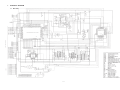
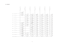
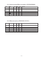
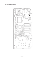
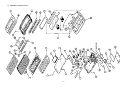
(with price)
SF-8350R(LX-523)
JAN. 1994
SF-8350R
R
CONTENTS
1.
SCHEMATIC DIAGRAM................................................................................................ 1
2.
SPECIFICATIONS ......................................................................................................... 5
3.
TO REPLACE THE BATTERY ...................................................................................... 6
4.
ERROR MESSAGE ....................................................................................................... 7
5.
TO RESET THE DIGITAL DIARY ................................................................................. 7
6.
TO SAVE THE DATA TO OTHER MACHINE ............................................................... 8
7.
TO CHECK THE MEMORY CAPACITY...................................................................... 11
8.
DISASSEMBLY ........................................................................................................... 12
9.
BLOCK DIAGRAM ...................................................................................................... 14
10.
CIRCUIT EXPLANATIONS
10-1.
System chart ................................................................................................. 15
10-2.
Power supply circuit .................................................................................... 16
10-3.
Battery voltage detection ............................................................................ 19
10-4.
CPU pin description (µPD3055GF002-2BA) ............................................... 21
10-5.
Gate array pin descriptions (µPD65005G-452-22) ..................................... 21
10-6.
Power supply chip IC pin descriptions (SC371015FU) ............................. 21
10-7.
Character generator ROM pin descriptions (HD62063B01) ..................... 22
10-8.
Operation program ROM pin descriptions (µPD23C2001EGW342) ......... 23
10-9.
RAM pin descriptions (µPD43256AGU-10/12/15LL) .................................. 23
11.
DIAGNOSTIC OPERATION ........................................................................................ 24
12.
TROUBLE SHOOTING................................................................................................ 29
13.
PARTS LIST ................................................................................................................ 32
14.
PCB VIEW ................................................................................................................... 34
15.
ASSEMBLY VIEW ....................................................................................................... 35
1.
SCHEMATIC DIAGRAM
1-1. Main PCB
—1—
1-2. Display PCB
—2—
1-3. Key Matrix
—3—
2.
SPECIFICATIONS
Data storage:
Telephone/business card/memo/schedule data storage/recall, calendar display, marker, phrase memory,
secret area, editing, capacity display, auto display
Clock:
Average of accuracy ±3 seconds per day under normal temperatures; worldtime, schedule alam, daily
alarm
Calculation:
12-digit arithmetic calculations, constants for + / – / × / ÷, independent memory, percentages, square
roots, 24-digit approximations, date calculations, other mixed calculations
Messages:
Selectable language:
English, German, French, Italian, Spanish, Swedish, Polish, Czech, Hungarian,
Russian
General:
Display element:
Memory capacity:
Main component:
Power supply:
32-column × 6-line LCD
64 KB (56,006 bytes)
LSI
Main Power Supply — Two CR2032 lithium batteries
Backup Power Supply — One CR2032 lithium battery
Power consumption:
0.05W
Battery life:
Main:
Approximately 120 hours (Repeated cycle of 1-minute data input
into Telephone Directory followed by 10-minute display. Operation
temperature of 20°C)
Approximately 150 hours (Continuous display in Telephone Directory. Operation temperature of 20°C)
Backup: 5 years if main batteries are replaced as soon as they become weak.
1 year if dead main batteries are left in the unit.
Auto power off:
Approximately 6 minutes after last key operation
Operating temperature: 0°C ~ 40°C (32°F ~ 104°F)
Dimensions:
Unfolded: 10.5H × 152W × 155.2mmD (3/8"H × 6"W × 61/8"D)
Folded:
17.9H × 152W × 78mmD (3/4"H × 6"W × 31/16"D)
Weight:
152.5g (5.4 oz) including batteries
Current consumption:
Power switch
TYP. [µA]
MAX [µA]
8
29
ON
1,447
13,258
ON (Operating)
6,707
19,958
OFF
—5—
3.
TO REPLACE THE BATTERY
A) To replace the main batteries
Before replacing the main batteries, note the following precautions.
• Do not remove the back-up battery from the SF Unit while main batteries are removed.
• Be sure to replace both batteries at the same time, and do not use an old battery with a new
one.
1. Remove the screw that hold the battery compartment cover in
place.
2. Remove the battery compartment cover by sliding it in the
direction indicated by the arrow in the illustation.
3. Slide the main battery holder in the direction indicated by the
arrow.
4. Remove both old batteries and replace with two new ones.
• Use two new batteries. Wipe the surfaces of the batteries with a
soft, dry cloth. Make sure that the positive (+) sides of the
batteries are facing up (so you can view the positive sides as the
batteries lie in the battery compartment).
5. Replace the battery holder.
6. Replace the battery compartment cover and fasten it in place
using the screw.
B) To replace the back-up battery
Before replacing the back-up battery, note the following precautions:
• Do not remove the main batteries from the SF Unit while back-up battery is removed.
• Be sure to replace the back-up battery at least once a year.
1.
2.
3.
4.
5.
6.
7.
Remove the screw that hold the battery compartment cover in
place.
Remove the battery compartment cover by sliding it in the
direction indicated by the arrow in the illustration.
First , remove this sticker from the back-up battery holder.
After removing this sticker, take the screw off that secures the
back-up battery holder in place, and then remove the battery
holder.
Remove the old battery and replace it with a new one.
• Wipe the surfaces of the battery with a soft, dry cloth.
Make sure that the positive (+) side of the battery is facing up (so
you can view the positive side as the battery lies in the battery
compartment.)
Replace the back-up battery holder and fasten it in place using
the screw, and replace the sticker over the battery holder.
Replace the battery compartment cover and fasten it in place
using the screw.
—6—
4.
ERROR MESSAGE
Message
Meaning
Action
Text specified for
search does not exist.
Correct or change
specified text.
Wrong password
entered.
Enter correct
password.
MEMORY FULL!
No more room in
memory for storage of
data.
Delete unnecessary
data items from
memory.
DATA ERROR!
CONSULT YOUR
OWNER'S MANUAL
UNDER "DATA
ERROR"
Abnormal data caused
by strong impact, static
electricity, etc.
Consult the "DATA
ERROR" section on
page 3 of owner's
manual.
DATA ITEM NOT
FOUND!
PASSWORD
MISMATCH!
5.
TO RESET THE DIGITAL DIARY
Before describing the RESET operation, a note of WARNING — The following procedure will erase
all data stored in memory, including marked data items. Be sure to perform the RESET operation
only if you wish to clear all data.
To reset the SF Unit's memory
1. Switch on power and press the RESET button with a thin, pointed object.
The following message appears on the display.
DELETE ALL DATA ITEMS
STORED IN MEMORY ?
YES Y / NO N
* Important!
Note that the following operation will clear everything stored in the unit's memory. To
avoid accidental erasure of important data, be sure to perform this operation only while the
system language is set to your native language. See page 2 of owner's manual for
infomation on how to change the system language.
2. Press Y to reset the SF Unit and clear everything from its memory. To abort the procedure
without clearing anything, press N .
—7—
Following the RESET operation, the Home Time Display appears. The initial settings of the SF Unit after
reset are shown below.
HOME TIME:
G.M.T.
JAN/1/1993 (FRI)
12:00 AM
12-hour format
WORLD TIME:
New York
Daily Alarm:
12:00 PM
Sound:
Schedule alarm
Daily alarm
Key
Character input:
CAPS
System Language: English
6.
ON
OFF
ON
TO SAVE THE DATA TO OTHER MACHINE
SF-8350R can transfer customers data to other SF-8350R with memory protection only when replacing
the LCD or the outer case. How to transfer the data.
* Before connecting the cable (SB-60 or SB-62), be sure to reset the slave machine to clear all
data.
Important!
* You can not perform data communications with the CASIO SF-A series of SF Units (SF-A10,etc.).
* Be sure to replace the connector covers on the SF units when you are not performing data communications.
1) Turn off the power switch and connect the two units using the cable (SB-60 or SB-62) as shown in
the drawing.
2) Turn on the power switch of each machine.
3) The slave machine must be set the date of Feb. 3rd, 1901 into the memory under the calculator
mode.
Operation:
CAL
ON
CLEAR/AC
1
9
0
1
TIME
DATE
2
TIME
DATE
3
TIME
M+
DATE
R
If you don't set the date, the "PASSWORD" isn't transferred to the slave machine.
—8—
4) Check the hardware parameters, and if the units have another condition, reset as follows.
To change the hardware
parameters, press the
,
,
and
cursol keys.
To set the hardware
parameters, press the set
key.
***
HARDWARE PARAMETERS
PARITY
BIT LENGTH7 bits
BPS
1200
EVEN
2400
***
ODD
7 bits
4800
NONE
8 bits
9600
TEL
TEL
FUNCTION
4
4
5) Set up the slave machine.
1
While in the Calender Display, Telephone Directory, Business Card Library, Memo Mode, or
Schedule Keeper, press the FUNCTION key followed by 4 to select " DATA COMMUNICATION", and the following menu appears.
TEL
FUNCTION
4
1
2
3
4
5
6
SEND
RECEIVE
PRINT
HARDWARE PARAMETERS
DATA TO RAM CARD
PEN PRINTING
TEL
2
Press 2 to select "RECEIVE" and the following display appears to indicate that the slave
machine is ready to receive data.
2
RECEIVE OK !
TO STOP, PRESS ESC
TEL
6) Set up the customer's machine.
1
While the transmitting unit is in the Calender Display, Telephome Directory, Business Card
Library, Memo Mode, or Schedule Keeper, press the FUNCTION key followed by 4 to select
"DATA COMMUNICATION", and the following menu appears.
TEL
FUNCTION
4
1
2
3
4
5
6
SEND
RECEIVE
PRINT
HARDWARE PARAMETERS
DATA TO RAM CARD
PEN PRINTING
TEL
—9—
2
Press 1 to select "TRANSMIT" and the following menu appears.
1 ONE DATA ITEM
2 MODE DATA ITEMS
3 ALL DATA ITEMS
1
— SEND —
TEL
3
Press 3 to select "ALL DATA ITEMS", and the following display appears to confirm
whether you wish to proceed.
SEND ALL DATA ITEMS ?
3
YES SET / NO ESC
TEL
4
Press the SET key to proceed with the data transmission, or press ESC if you wish to cancel.
SET
NOW SENDING !
TO STOP, PRESS ESC
Data are transmitted in the sequence of Telephone Directory data, Business Card Library data, Memo
data, Schedule Keeper data and Calendar data.
* If the customer's machine uses full memory, it takes about one minute and ten seconds for this
transferring.
* The following messages appear on the display of the receiving unit when a problem occurs during
data communications. All data transferred up to display of the message is retained in memory, but
data communication is terminated.
TEL
BUSINESS CARD
MEMO
SCHEDULE
If one of the following error messages appear, press the
,
,
,
,
HOME TIME
, WORLD TIME , CAL , CALENDAR key, to clear the error message. Then, take corrective
action and try data communication again.
— 10 —
Message
STOPPED !
7.
Cause
• ESC key pressed on transmitting or receiving unit.
• Memory area of receiving unit full.
• Battery power drops below a certain level.
TRANSMIT ERROR !
Cable connection broken or abnormal noise in cable.
MEMORY FULL !
Memory area of receiving unit full.
TO CHECK THE MEMORY CAPACITY
The memory Capacity display tells you how much total memory is used for storage of Telephone
Directory, Business Card Library, Memo, Calendar, and Schedule Keeper data. It also shows the
percentage of total memory used, and how much total memory area remains. Press the CAPA key to
check the current memory capacity.
Following the memory reset operation, the display will appear as follows.
56006
0
0
When the percentage of memory used reaches 100%, you will not be able to enter any more data into
memory.
— 11 —
8. DISASSEMBLY (SF-8350R)
1) To open display unit
1. Remove the key switch sheet from the display frame with care using a sharp tweezers and
remove 2 screws, then remove the display back cover.
2. Remove the blind plate of hinge and then release the 2 screws of hinge cover.
3. Release the 5 screws of display PCB and remove the display PCB.
— 12 —
2) To open battery cover and back cover
1. Release the one screw of battery cover and remove the battery cover.
2. Remove the batteries. (Refer section 3 in this manual.)
3. Release the 8 screws of the back cover. Then, remove the back cover.
4. To check the circuit by oscilloscope, apply the power to main PCB as follow:
External Power supply
Switch
GND
Prepare some 2P switch for Main switch.
+6V
+3V
Prepare some power supply for + 6V and +3V.
— 13 —
9. BLOCK DIAGRAM
LCD
192 X 48 dots
CD401-TS
S32~S111
S0~S31
C0~C47
S112~S191
LCD DRIVER
LCD DRIVER
LCD DRIVER
MSM6585AV
-Z-358B
MSM6585AV
-Z-358B
MSM6585AV
-Z-358B
DATA BUS
TO KEYBOARD
LCD DRIVE VOLTAGES
V1 ~ V4, VREG
CPU
POWER SUPPLY
CHIP FOR LCD
µPD3055GF002-2BA
SC371015FU
VDD
OPEN (OFF)
LOCK (ON)
ROM
MAIN SWITCH
(Character Generator)
CARD LOCK SWITCH
GND
HD62063B01
FREE (OFF)
LOCK (ON)
Power supply circuit
ROM
(Operation Program)
µPD23C2001EGW342
NOTE
GATE ARRAY
RAM
µPD65005G-452-22
µPD43256AGX10/12/15LL
X 2 PCS.
TX, RX
— 14 —
INTERFACE FOR
DATA TRANSMISSION
& DATA RECEPTION
10. CIRCUIT EXPLANATIONS
10-1. System chart
Generally, SF-8350R is working with the following steps.
VDD
11
"H"
(Pin30)
(Pin31)
12
PDB
2
(Pin3)
VDD
VO1
VREG,V1~V4
Output
for LCD
drive
Power supply chip
SC371015FU
(Pin2)
VDD1
GND
VDD2
(Pin20)
(Pin32)
1
(Pin17)
(Pin39)
VDD
VOT
GND
Gate array
(Pin29)
(Pin24)
LSI
µPD65005G-452-22
VIN
MON
Open
SWO
VOB
LSO
(Pin35)
(Pin25) (Pin40)
Batteries
CR-2032 X 2 pcs.
4
3
13
"H"
"L"
"L"
Transistor Q1
"H"
(Pin2)
VDD
2 MHz
10
(Pin69)
(Pin45)
(Pin41)
V2ON
INIT1
OSCI
9
(Pin1)
(Pin3)
(Pin40)
OSCO
VDD
VDD
VDD
(Pin70)
14
INT0
OFF
CPU
GND
"H"
MAIN SWITCH
SW
µPD3055GF002-2BA
(Pin36)
6
"L"
5
ON
VCC
EO
KIO
KAC
(Pin54)
(Pin53)
(Operation program)
15
"H"
"L"
GND
ROM
(Pin30)
(Pin22)
µPD23C2001EGW342
CEB
"L"
7
8
16
ADDRESS
ADDRESS BUS
DATA BUS
17
9.
10.
11.
12.
13.
14.
15.
CPU oscillation is generated.
Output "H" from V2ON terminal.
Output "H" from VOT terminal.
Output all LCD drive voltages.
Output "L" from VOB terminal.
Apply VDD to ROM.
CPU sends ROM chip enable
signal from EO terminal.
16. CPU sends address to ROM.
17. CPU receives data from ROM.
1. Supply 6V to VDD1 and VDD2.
2. Output VDD (4.5V).
3.
4.
5.
6.
7.
8.
DATA
Output "L" from SWO terminal.
Output "H" from LSO terminal.
Main switch ON.
Input "L" to SW terminal.
Output "L" from KAC terminal.
Push power on button switch.
— 15 —
10-2.Power supply circuit
1) Power supply chip SC371015FU
+
C8
21
18
+
C7
20
17
16
R8
R9
R10
The IC SC371015FU is power supply chip for SF8350. When IC SC371015FU receives a Voltage
6V (CR-2032 × 2 pcs.) at the terminal VDD1(Pin
No.2), the regulated voltage VDD (4.3~4.7V) will
be applied to the VDD lines. The outputs Vss
(VREG) and V1~V4 are the LCD drive voltages.
When the terminal PDB becomes "H", those voltages are generated by IC SC371015FU and capacitors C7 and C8 (ESCT1AY335R) and applied
to LCD driver IC MSM6385AV-Z-358B.
The resistors R8~R10 are used for dividing voltage V1~V4.
VREG 8
15
V1
14
V2
POWER SUPPLY CHIP
13
V3
SC371015FU
9
10
11
V4 12
V COMP1
V COMP2
VO1
VDD1
VDD2
6
7
2
1
VDD
(4.3 V ~ 4.7 V)
19
LCD DRIVE VOLTAGE
PDB
31
GND1
32
GND2
22
Value (Approx.)
[V]
Contrust : Min.
Contrust : Max.
VSS(VREG)
-3.5
-6.4
V1
+3.4
+3.1
V2
+2.5
+1.7
V3
-1.5
-3.6
V4
-2.5
-4.9
FROM
GATE ARRAY
VOT terminal
CR2032
Memory battery
CR2032
CR2032
Main batteries
The V comp1 and V comp2 outputs are the battery voltage detection outputs. According to
VDD1 and VDD2 voltages, V comp1 and V comp2 will change the status as follows:
OUTPUTS
V COMP 1
V COMP 2
STATUS " H "
STATUS " L "
When the batteries voltage
When the batteries voltage
is more than 4.7 V.
is less than 4.6 V.
When the batteries voltage
When the batteries voltage
is more than 4.5 V.
is less than 4.4 V.
— 16 —
2) Gate array
When VDD is applied from power supply IC
SC371015FU to gate array uPD65005G-45222, gate array will send "L" signal to active the
main switch signal from terminal SWO. Also,
gate array will send "H" signal to release the
INT0 terminal of CPU from LSO terminal.
The terminal CSB is for the chip select of gate
array. This signal is sent from CPU terminal
CS2. And when the VDD is applied to CPU,
CPU will send "H" signal to CSB terminal.
GND
Open
(Pin 23)
(Pin 24)
TO MAIN SWITCH
"L"
(Pin 40)
LSI
MON
SWO
GATE ARRAY
"H"
TO CPU
INT0 terminal
(Pin 70)
(Pin 25)
µPD65005G-452-22
LSO
(Pin 39)
(Pin 17)
VDD
GND
CSB
(Pin 22)
"H"
FROM CPU
CS2 terminal (Pin 28)
3) Main switch and power on switch
VDD
MAIN SWITCH
(Pin36)
SW
"L"
CPU
KAC
"L"
ON
GATE ARRAY
(Pin40)
"L"
µPD3055GF002-2BA
(Pin54)
OFF
SWO
µPD65005G-452-22
KIO
(Pin53)
"H"
POWER ON SWITCH
When the main switch is set to on position, SW terminal of CPU becomes "L", then CPU will send
"L" signal to KAC terminal to enable the system power on. The KI0 terminal is "H" when VDD is
applied to CPU. Therefore, when pressing the power on switch, CPU will generate a clock pulse (2
MHz) for start up the system.
— 17 —
4) Power supply for LCD
(Pin30) "H"
(Pin69)
CPU
(Pin31)
PDB
VOT
INT1
V2ON
µPD3055GF002-2BA
"H"
(Pin45)
(Pin29)
POWER SUPPLY CHIP
VIN
SC371015FU
GATE ARRAY
µPD65005G-452-22
LCD drive voltages
VREG,V1~V4
When the system is start up, CPU will send "H" signal to VIN terminal of gate array from V2ON
terminal. Then, gate array will send "H" signal from VOT terminal to release interruption signal
INT1 of CPU and also, it will be sent to PDB terminal of power supply chip to generate LCD drive
voltages.
5) ROM driving transistor
VDD
(Pin1)
R4
" L " (Pin35)
(Pin2)
Transistor Q1
(Pin3)
VOB
(Pin30)
VCC
GATE ARRAY
µPD65005G-452-22
VDD
E0
ROM
µPD23C2001
DATA
CPU
EGW342
ADDRESS
µPD3055GF002-2BA
After gate array send VOT signal, gate array send "L" signal from VOB terminal to base terminal of
transistor Q1. Then, the VDD is applied to ROM (operation program), CPU can read a ROM
program data by E0 signal.
— 18 —
10-3.Battery voltage detection
(Pin32)
(Pin22)
(Pin1)
GND1
GND2
(Pin7)
(Pin79)
Power Supply Chip
SC371015FU
(Pin6)
VCOMP1
(Pin37)
VCOMP2
P7
ONMK
VDD1
CPU
VDD2
(Pin19)
µPD3055GF002-2BA
CR-2032 X 2
Main batteries
The power supply IC chip SC371015FU has
two kind voltage detection circuit in it. According to the batteries input voltage, the detection
outputs V comp1 and V comp2 will change the
status as follow:
VCOMP2
(Pin27)
BLI
Gate Array
µPD65005G-452-22
Batteries Voltage
VCOMP2
More than about 4.6V
"H"
Less than about 4.6V
"L"
VCOMP1
Batteries Voltage
VCOMP1
More than about 4.4V
"H"
Less than about 4.4V
"L"
When CPU receive VCOMP2 detection signal, the machine shows "MAIN POWER SUPPLY
BATTERIES GETTING WEAK! REPLACE!" on the display. And when the batteries voltage is
weak more (approx. 4.53V), as the VCOMP1 detection signal becomes "L". The machine will
operate an auto power off operation.
— 19 —
10-4.CPU pin description (µPD3055GF002-2BA)
Pin No.
Name
In/Out
Status
Status
Description
of ON
Pulse
GND
Pulse
Pulse
Pulse
H
H
Pulse
Pulse
H
H
H
H
L
L
H
L
Pulse
H
H
H
H
H
Pulse
Pulse
L
H
H
H
H
H
H
H
H
Pulse
Pulse
H
H
H
L
H
H
L
Pulse
H
Pulse
Pulse
Pulse
Pulse
Pulse
Address Bus line
GND terminal
Write signal
Read signal
Not used
Not used
Chip select signal for gate array
(Character generator)
Chip select signal for ROM (Chargacter
generator)
Chip enable signal for ROM (Operation program)
Chip enable signal
Chip enable signal
Chip enable signal
BCN signal to gate array
MDP signal to gate array
Switch signal (When switches are at ON position.)
Battery detection V comp1 input
TEST terminal (connect to GND)
Clock input
Power input for Clock
VDD input terminal
VDD input terminal
Power on output signal
Key input signal (KI7---Not used)
Power on switch signal output
Key common signal output
GND terminal
Interrupt signal from ROM (Character generator)
Interrupt signal from gate array
Interrupt signal from gate array
VDD input terminal
Transmission data output
Reception data input
Card lock switch input
IC card detection signal input
KC12 key common signal output
KC13 Key common signal output
Memory back-up battery detection input
Battery detection V comp2 input
Display contrast control signal output (Up/Down)
GND terminal
Not used
Chip enable signal for gate array
Display contrast control clock signal
Not used
LCD driver mode selection signal
LCD driver synchronous signal
LCD driver latch pulse signal
Not used
LCD driver data latch clock signal
Data bus line
Pulse
Address line (Used only RA15,16)
1~14,16,17
15,39,100
24
25
26
27
28
29
30
31
32
33
34
35
36
37
38
40,41
42
43,91
44
45
46~53
54
55~65,67
66
68
69
70
71
72
73
74
75
76
77
78
79
80
81
82
83
84
85
86
87
88
89
90
92~99
A0~A15
VSS
WE
OE
FE
CS1
CS2
CS3
E0
E1
E2
E3
BCON
MDP2
SW
ONMK
TEST
OSC O/I
VOSC
VDD1
VDD2
V2ON
KI7~KI0
KAC
KC0~KC11
GND
INT2
INT1
INT0
BRK
P0
P1
P2
P3
P4
P5
P6
P7
H1
WENL
H2
L1
L2
DT
PRO
FR
LP
GC
DE
IO7~IO0
Out
In
Out
Out
Out
Out
Out
Out
Out
Out
Out
Out
Out
Out
In
In
In
In
In
In
In
Out
In
Out
Out
In
In
In
In
In
Out
In
In
In
Out
Out
In
In
Out
In
Out
Out
Out
Out
Out
Out
Out
Out
Out
In/Out
of OFF
L
GND
H
H
H
H
H
H
L
L
L
L
H
H
L
H
L
L
L
H
H
L
H
L
H
L
H
L
H
H
H
L
H
L
H
H
H
H
H
L
H
L
L
H
L
L
H
H
H
L
18~23
RA14~19
Out
L
— 20 —
10-5.Gate array pin descriptions (µPD65005G-452-22)
Pin No.
1~8
9
10,11
12
13~16,18~21
17
22
23
24
25
26
27
28
29
30
31
32
33
34
35
36
37
38
39
40
41
42
43
44
Name
OI7~OI0
A15
A01,A00
CEB
IO0~IO7
GND
CSB
MON
LSI
LSO
PDN
BLI
DEB
VIN
VOT
OEI
WEI
BBC
CDE
VOB
TXO
TXI
FOM
VDD
SWO
BCN
MDP
OEO
WEO
In/Out
Status
Status
Description
In/Out
In
In
In
In/Out
In
In
Out
In
Out
In
In
Out
In
Out
In
In
Out
In
Out
Out
In
In
In
Out
In
In
Out
Out
of OFF
L
L
L
L
L
L
H
L
L
H
H
H
H
L
L
H
H
L
L
H
H
H
H
H
L
H
H
L
L
of ON
L
Pulse
Pulse
Pulse
Pulse
L
Pulse
L
L
H
H
H
Pulse
H
H
Pulse
Pulse
Pulse
H
L
H
H
H
H
L
H
L
Pulse
Pulse
card
Data
bus line for ICcard
Not used
Address input
A1,A0 address input
Decode signal for data access
Data bus line
GND terminal
Chip select signal from CPU
Not used
Holding
signal for LSI terminal (Card lock switch)
Card lock switch
detection input
Connected
to GND
Card lock switch detection output
Power down detection input
Battery detection V comp1 input
Chip selection signal for ROM(Character generator)
Power on signal input
Power on signal output
Read signal input
Write signal input
Memory back-up battery scanning signal
IC card detection signal input
ROM power switching signal (Operation program)
Transmision data output
Reception data input
VDD terminal
VDD terminal
Main switch control signal
BCON signal from CPU
MDP2 signal from CPU
Read signal for IC card (Not used)
Write signal for IC card (Not used)
10-6.Power supply chip IC pin descriptions (SC371015FU)
Pin No.
Name
In/Out
Status
of OFF
Status
of ON
Description
32,22
1,19
2
31
6
7
8
9
10
11
12
13~16
17
18
20
21
23
GND1,2
VDD1,2
VO1
PDB
V COMP1
V COMP2
VSS
V1
V2
V3
V4
VD/V1~4
C1N
C2P
C1P
C2N
SUB CONT
In
In
Out
In
Out
Out
Out
Out
Out
Out
Out
**
**
**
**
**
In
L
H
H
L
H
H
L
L
L
L
L
H
GND
3V
3V
GND
L
L
H
H
H
H
H
*-5V
*3.25V
*1.95V
*-2.5V
*-3.75V
**
-5V
GND
-2.2V
-2.2V
**
GND terminal
Main battery positive terminal (+6V)
VDD output terminal (4.5V)
Power on switch signal from gate array
Battery detection signal (less than 4.6V---"L")
Battery detection signal (less than 4.4V---"L")
LCD drive power V REG
LCD drive power V1
LCD drive power V2
LCD drive power V3
LCD drive power V4
Voltage drividing terminal for LCD drive power
Negative terminal for doubler capacitor C7
Positive terminal for doubler capacitor C8
Positive terminal for doubler capacitor C7
Negative terminal for doubler capacitor C8
— 21 —
Pin No.
Name
In/Out
Status
of OFF
Status
of ON
Description
24
25
26
27
28
29
30
31
EROUT
VFB
MIN
MAX
U/D
CLOCK
SET
PDB
Out
**
**
**
In
In
In
In
6V
H
5V
5V
H
L
H
L
5V
3.2V
3.2V
3.2V
5V
L
H
H
VFB capacitor terminal
EROUT signal input
Display contrast control signal (Up/Down)
Display contrast clock signal
Display contrast data reset signal
10-7.Character generator ROM pin descriptions (HD62063B01)
Pin No.
Name
In/Out
**
In
In
Power
In
In
Out
In
In
Power
In
Out
Status
of OFF
L**
L**
3V
L
H
Pulse
**
H
H
L
H
**
H
Status
of ON
L
**
**
L
**
3V
LH
Pulse
**
H
H
L
H
**
H
1,7~12,23
2
3
4,20
5,6
13
14,19
15,32
16,21
17,22
NC
BLD
VOSC
GND
OSI/OSO
TNL
IN1+,IN2+
VSS1,VSS2
IN1-,IN2OUT1,OUT2
18
24
25
26,27
28
29,30
31
33
34~37
38~42
43
44
TNH
IN
OUT
BZ1,2
INT
CEH,CEL
CED
EN
IO3~IO0
A0~A3,A15
WEB
CSB
Description
Not used
Not used (Battery voltage detection terminal)
Connected capacitor
GND
VDD terminal
terminal
External clock terminal (32.768 KHz)
Not used
Connected to VDD
GND terminal
Connected to VDD
Not used
Out
In
Out
Out
Out
Out
In
In
In/Out
In
In
In
H
**
L
H
L
H
H
H
L
L
L
H
H
H
**
Pulse
Pulse
L
H
Pulse
Pulse
H
Pulse
Pulse
Pulse
Pulse
Not used
Power on key input terminal
KI0 terminal for power on
Buzzer signal
Interrupt signal for alarm clock (alarm time----"L")
RAM chip select signal
Chip enable signal of CPU
Enable signal (Buzzer off-----"L")
Data bus line (IO0~IO3)
Address bus line (A0~A3,A15)
Write signal
Chip select signal
— 22 —
10-8. Operation program ROM pin descriptions (µPD23C2001EGW342)
Pin No.
Name
In/Out
Status
of OFF
Status
of ON
Description
1,30,31
2~12, 23,
25~29
13~15, 17~21
16
22
24
32
NC
A0~A16
In
L
L
+5V
Pulse
Connected to VCC
Address bus line (A0~A14,RA15,RA16)
IO0~IO7
GND
CE
OE
VCC
Out
Power
In
In
Power
L
GND
L
L
L
Pulse
GND
Pulse
Pulse
+5V
Data bus line (IO0~IO7)
GND terminal
Chip selection terminal
Output enable terminal
VCC terminal
10-9. RAM pin descriptions (µPD43256AGU-10/12/15LL)
Pin No.
Name
In/Out
Status
of OFF
Status
of ON
Description
2, 4~6, 9~13,
15~18
21~23, 25~29
24
31
1
7
8
A0~A14
In
L
Pulse
Address bus line (A0~A14)
D1~D8
GND
CSB
OEB
WEB
VCC
In/Out
In
In
In
In
In
L
L
H
H
H
H
Pulse
L
Pulse
Pulse
Pulse
H
Data bus line (IO0~IO7)
GND terminal
Chip select signal
Read signal from CPU
Write signal from CPU
VDD terminal
— 23 —
11. DIAGNOSTIC OPERATION
Main switch
Check pad
1. Diagnostic mode
SELECT MENU
1 DISPLAY
2 MEMORY
3 KEY
4 BUZZER
5 I/F
The diagnostic mode appears when main switch is turned on
while there is a short in the checkpad. After this operation,
the machine will beep and display "SELF-TEST".
The menu appears after press SET key. Tests are conducted
by selecting the mode from the list on screen. The each test
can be selected by the following function keys.
TEL key
Business card key
MEMO key
SCHEDULE key
CALENDAR key
: Test the LCD display
: Test the IC memory chip and the RTC
: Test all keys
: Buzzer test
: SB-60/SB-62cable interface
2. Display check
DISPLAY
1 WHITE
2 BLACK
3 CHECKER
4 REVERSE
5 FRAME
DISP CHNG key
TEL key
Business card key
MEMO key
SCHEDULE key
CALENDAR key
— 24 —
: Return to menu display
: Lights on dot at corners
: Lights on in all dots(black screen)
: Checker display
: Reverse checker display
: Lights on dot along the screen edge (frame)
3. ROM/RAM check
DISP CHNG key
MEMORY
INT #1
1 WRITE
2 READ
3 DUMP
4 CHKSUM
5 RTC
INT---Internal RAM
EXT--External RAM(RAM card)
#1---Test data pattern(00,01,02...)
#2---Test data pattern(FF,FE,FD....)
:Return to menu
TEL key
:Write the set pattern to the selected RAM
area
Business card key :Compare the pattern displayed after # with
the write data of RAM and displays the
results.
MEMO key
:Dump contents of memory. (direction
depens on setting of internal/extarnal
switch)
SCHEDULE key :Call up checksum and XOR values for
connected ROM/RAM data.
CALENDAR key :Bring up clock display. The present time,
data and daily alarm can be set.
NOTE 1. To change the RAM internal or extenal, press WORLD TIME key. As SF-8350 has no RAM
card interface, Test only Internal RAM area.
NOTE 2. To change the test data pattern,
press HOME TIME key for data pattern 1 (00,01,02,03,......FF,00,01,02,03,......).
press WORLD TIME key for data pattern 2 (FF,FE,FD,......00,FF,FE,FD,...........).
1) RAM write
The following message will be displayed while writing the data to RAM.
When there is no RAM to write a data,
the following message will be displayed.
EXECUTING !
NO RAM
To release this message, press DISP CHNG key.
2) RAM read
Normal end display is;
COMPLETE !
64KB
Error end display is;
DATA ERROR !
ADDRESS
XXXX
CORR
XX
RAM
XX
To release this message, press DISP CHNG key.
— 25 —
3) Memory dump
When memory dump is operated by pressing MEMO
button, a display will appear as shown at left. The
first two lines, begining from the top left, signify the
following address values in reference to the one
megabyte "E0" area:
00001,00002,00004,....,00080,00100,00200
00400,00800,01000,....,20000,40000,80000
The lower two lines refer to the data in the "E1" area.
MEMORY DUMP
XX
XX
XX
XX
XX
XX
XX
XX
XX
XX
XX
XX
XX
XX
XX
XX
XX
XX
XX
XX
XX
XX
XX
XX
XX
XX
XX
XX
XX
XX
XX
XX
XX
XX
XX
XX
XX
XX
XX
XX
Note : The Internal/External switch is activated
pressing CAL button. SF8350 has no external RAM area.
4) CHECK SUM
TYPE
E0 ROM
CE
RAM
5)
RTC
SIZE CHECK-SUM XOR
128KB
DB98
4F
64KB
8300
00
TIME DISPLAY
yyyymmddhhmmss........
..............
1990 04 04 12 34 56
Type : ROM and RAM are shown.
However, if the ROM is not in
standard Casio format, a format
error will be displayed.
Size : Memory capacity (total)
Checksum:
XOR : Logic operation for all data.
Input can be made in the second and
third lines using the numeric keys.
Entry of 12 or more digits sets the time
and date. Entry of 4 or 6 digits sets the
daily alarm. The ON key clears current
entries.
The ON key is the only key that remains
functional when an error has occurred
or check-sum is being displayed.
4.
Key check
KEY
1 RANDOM
2 AUTO
TEL Key
:
The 'key code' will be displayed.
The 'key code' is numbered incrementally from
left to right with the DISPLAY CHANGE key as
"00", and TEL key as "01" etc. Accordingly,
the SET keys is "81". To release this test, press
SEARCH key.
Business card key :
Limits the mode mentioned above so that the
keys must be pressed in order according to the
key code. If an error is made a buzzer sounds
for about 1 second. (A correct entry results in a
beep tone)
In either mode a press of the SEARCH key will return the screen to the menu mode.
— 26 —
5. Buzzer check
BUZZER
1 BEEP
2 ALARM 1
3 ALARM 2
TEL key
: Key input sound every 1 second
Business card key : Sound alarm 1
MEMO key
: Sound alarm 2
Sound can be stopped by pressing the any key.
While an alarm is sounding the screen display is as shown at
left. If an irregularity is found in voltage of battery while the
alarm is sounding, the alarm will stop. After 256 seconds, the
alarm will stop automatically.
EXECUTING !
6. SB-60/SB-62 cable interface check
I/F
1 TRANSMIT
2 RECEIVE
3 LOOP
4 ASCII
7N9
Parameter
EXECUTING !
The TEL to SCHEDULE keys are used to select mode; the
CALENDAR, HOME TIME and WORLD TIME key are used
to set the transmission paraments. The three charactors that
appear on the right side at display represent the parameter.
In the case of the exampledisplay, it indicates 7 BIT, NON
PARITY, 9600 BPS. The operation continues until stopped by
pressing the ESC key and then pressing the ON key for all
modes.
DISP CHNG key : Return to menu mode
TEL key
: Transmission mode. The data of transmission
is "H" and it is sent out by the data of &H34 and
&H38 by the Xon/Xoff control.
Business card key : Reception mode. Make sure to set the
parameter to match that of the transitting side.
The data received appears on the display.
MEMO key : Loop back test. Short the Tx and Rx terminals
for this test. Transmit and check from &H20 to
&H7E. When complete, the message 'CHECK
COMPLETE' is displayed.
SCHEDULE key : output the following ASCII code by Xon/
Xoff control.
!"#*+,-/0123456789:
ABCDEFGHIJKLMNOPQRSTUVWXYZ
abcdefghijklmnopqrstuvwxyz
A line end code is added with each line.
CALENDAR key : Switch the data length 7 bit(7) or 8 bit(8)
HOME TIME key : Switch the parity bit : NON(N)—EVEN(E) —NON(N) —ODD(O)
WORLD TIME key : Switch the transmission speed : 9600(9)—4800(4)—2400(2)—1200(1)
To communicate two machines, please set the transmission machine before setting the receiving unit.
To release communication, press ESC button. In this case, the break code is sent to receive units.
Therefore, both machines display "TRNS BREAK !" and communication will be stopped. Also, if the error
is occurred, both machines display "TRNS ERROR !" and communication will be sttoped.
— 27 —
NOTE : As diagnostic program area does not have all ASCII code, to display a reception data, some
charactor will be changed to other charactor. For example, a chapital letter will be changed
to small letter.
Error display
Break display (Broken transmission)
TRNS ERROR !
TRNS BREAK !
7. Btattery level check
Memory back up battery
The memory back up voltage detector detects any
irregularity in voltage, the machine goes into an
error state and the display is as shown at left figure.
To release this display, press any key.
LOW BATTERY!
BACK UP
Main battery
When the main battery voltage detector detects
low battery condition while display is on, the machine shows the message as shown at left figure.
When this message is displayed, only ON/OFF
key are possible to operate. And if the voltage
becomes lower than 4.4V, the display will be off
mode (auto power off mode).
LOW BATTERY!
8. Others
1) When power is off after presetting a alarm time, automatically power is on at a alarm time.
However, the display is not reserved in this case.
2) When executing memory sum check, before execute the RAM write check (with TEL button).
3) To release diagnostic mode, press reset button.
4) The display contrast can be changed by the contrast volume.
— 28 —
12. TROUBLESHOOTING
Generally, check the machine with the followning steps for repair.
CONDITION : Card lock switch
LOCK
START
No
Main battries 6V?
Yes
Replace main battries (CR2032 2pcs.)
(Clean and adjust battery contact.)
1
Key input OK?
Yes
No
Reset operation
No
Display OK?
Yes
Yes
Save data to P/C if necessary.
Key input OK?
No
Current consumption OK?
No
Yes
Follow repair section 2.
Load data from P/C if necessary.
Follow repair section 1.
No
Data OK?
Yes
Follow repair section 3.
END
Repair section 1 : For no key input problem
START
No
Pin 2 of SC371015FU Approx. 4.5 V ?
Yes
Poor connection?
No
Yes
Solder line
1
Replace parts.
Pin 24 of µPD65005G-452-22 "L"?
Yes
No
Poor connection?
Yes
Solder line
No
1
Replace parts.
Pin 40 of µPD65005G-452-22 "L" ?
No
Poor connection?
Yes
Solder line
No
Yes
1
Replace parts.
Pin 36 of µPD3055GF002-2BA "L" ?
Yes
No
Poor connection?
Yes
Solder line
No
1
Replace parts.
Pin 54 of µPD3055GF002-2BA "L" ?
No
Poor connection?
Yes
Yes
Solder line
No
Replace parts.
2
— 29 —
1
2
Connection of keyboard cable OK?
Yes
When press power on Key, any
oscillation at oscillator?
No
1
Adjust keyboard cable.
No
Poor connection
on oscillator?
Yes
Yes
Solder line
No
1
Replace parts.
Pin 45 ofµPD3055GF002-2BA "H" ?
No
Poor connection?
No
Yes
Yes
Solder line
1
Replace parts.
Pin 29 of µPD65005G-452-22 "H" ?
Yes
Pin 30 of µPD65005G-452-22 "H" ?
No
Solder line
No
Poor connection?
Yes
Solder line
No
Yes
1
Replace parts.
Pin 31 of SC371015FU "H" ?
1
No
Poor connection?
Solder line
Yes
Pin 35 of µPD65005G-452-22 "L" ?
No
Poor connection? Yes
1
Solder line
No
Yes
1
Replace parts.
No
Poor connection?
Pin 3 of transistor Q1 "H" ?
Yes
Yes
Solder line
No
1
Replace parts.
Pin 32 of ROM µPD23C2001EGW342 "+4.5V" ?
No
Solder line
1
Yes
No
Pin 22 of ROM µPD23C2001EGW342
"Pulse" ?
Yes
Poor connection Yes
on ROM or CPU?
Solder line
No
1
Replace CPU.
Poor connection on ROM, RAM or CPU ?
Yes
Solder line
No
Replace ROM, RAM or CPU.
— 30 —
1
Repair section 2 : For no display or wrong display problem
START
Pin 30 of µPD65005G-452-22 "H" ?
No
Poor connection?
Yes
Solder line
No
Yes
1
Replace parts.
No
Solder line
Pin 31 of SC371015FU "H"?
Yes
LCD drive voltages OK?
(Pin8~12)
Yes
No
Poor connection?
1
Yes
No
Poor connection on chip Yes
resistors R8~R10 ?
No
Poor connection on chip Yes
capacitor C7~C8 ?
No
Chip capacitor OK ?
Yes
Chip resistor OK?
Yes
Solder line
No
No
Replace parts.
Replace SC371015FU.
1
Yes
Replace heat seal.
Poor connection or cut of heat seal cable ?
1
No
Poor connection on LCD driver ?
No
Yes
Poor connection or cut of heat seal cable for LCD ?
Solder line
Yes
1
Replace heat seal.
1
Replace LCD.
1
No
LCD cracked ?
No
Yes
Repleace Display PCB ass'y.
1
Repair section 3 : For memory problem
START
Poor connection on RAM chips ?
No
Poor connection on CPU ?
No
Yes
Yes
Solder line
1
Replace RAM chips or CPU.
— 31 —
13.
N
PARTS LIST (SF-8350R)
Item
Code No.
N
LSI7
LSI8
LSI6
LSI4
LSI3
LSI2
LSI1
X1
Q3
Q1
D1
D2
C13
C9
C7,C8
C12
C19
C5,C6,C15,
C18,C22,C23
C21
C10
C1
C2
C3,C4
C16,C17
R1,R28
R19
R5
R4
R17
R15
R25
R2
R14
R13
R6,R23,R24
R3,R8,
R9,R26
R16
R22
J1
X2
R7
N
1
2
3
4
5
Notes:
N
M
R
Q
Parts Name
Specification
1. CPU BOARD ASS'Y
2011 7112 LSI (ROM)
2011 2849 LSI (RAM)
2011 2849 LSI (RAM)
2010 8113 LSI
2011 1645 LSI
2105 2436 LSI
2011 0098 LSI
2590 0777 Ceramic oscillator
2259 0959 Chip digital transistor
2250 0413 Chip transistor
2390 1197 Diode
2390 0364 Diode
2895 1204 Chip tantalum capacitor
2895 1190 Chip tantalum capacitor
2895 1197 Chip tantalum capacitor
2845 1925 Chip capacitor
2895 1365 Chip capacitor
2845 1540 Chip capacitor
2845 1540
2845 2030
2845 2289
2845 2968
2845 2499
2845 1652
2795 3346
2795 4214
2795 3367
2795 3374
2795 3017
2795 3003
6511 7460
2795 3101
2795 2947
2795 2940
2795 2926
2795 3360
Chip capacitor
Chip capacitor
Chip capacitor
Chip capacitor
Chip capacitor
Chip capacitor
Chip resistor
Chip resistor
Chip resistor
Chip resistor
Chip resistor
Chip resistor
Chip resistor
Chip resistor
Chip resistor
Chip resistor
Chip resistor
Chip resistor
2795 3360
2795 3360
3501 6538
7110 0642
2765 1001
6409 4540
Chip resistor
Chip resistor
Miniature jack
Crystal oscillator
Volume
CPU board assembly
(Consists of the above parts)
6511 7420 Heat seal
6512 3150 Insulation seal
2. DISPLAY BOARD ASS'Y
2011 1974 LSI
3335 3612 LCD
6511 7710 Heat seal
– New parts
– Minimum order/supply quantity
– Rank
– Quantity used per unit
— 32 —
Q M
FOB Japan
N.R.Yen
R
Unit Price
µPD23C2001EGW342
µPD43256AGU-10,12LL
µPD43256AGU-10,12LL
HD62063B01
µPD65005G-452-22
SC371015FU
µPD3055GF002-2BA
CSAC2.01MGCM001-TC
DTC114YKT-14671K
2SA1141-T1B(M6)
MA743-(TX)
MA713-TX
ECST0J106R
ECST1AX106R
ECST1AY335R
MCH312F105ZP
MCH325F474ZP
MCH212F104ZK
1
1
1
1
1
1
1
1
1
1
1
1
1
1
2
1
1
6
1
1
1
1
1
1
1
1
20
20
10
10
20
10
20
20
20
20
670
600
600
510
230
540
870
98
12
24
36
33
29
39
29
21
27
4
A
A
A
A
A
A
A
B
C
C
C
C
C
C
C
C
C
C
MCH212F104ZK
MCH215C102KK
MCH215C471KK
MCH215C221KK
MCH215A300JK
MCH215A180JK
MCR03EZHJ105
MCR03EZHG304
MCR03EZHJ224
MCR03EZHJ154
MCR03EZHJ104
MCR03EZHJ473
CC4702310C1
MCR03EZHG363
MCR03EZHJ182
MCR03EZHJ102
MCR03EZHJ101
MCR03EZHJ000
1
1
1
1
2
2
2
1
1
1
1
1
1
1
1
1
3
4
20
20
20
20
20
20
20
20
20
20
20
20
20
20
20
20
20
20
4
3
3
3
3
3
2
4
2
2
2
2
9
4
2
2
2
2
C
C
C
C
C
C
C
C
C
C
C
C
C
C
C
C
C
C
MCR03EZHJ000
MCR03EZHJ000
HSJ1169-012010
DT-26S
RK09G-J11TS-100KB
DB04CX3101M
1 20
1 20
1 5
1 10
1 5
1 1
2
2
56
57
83
5,470
C
C
X
B
C
A
FX201P20172
HGFC0007905
1 5
2 10
78
30
A
X
MSM6385AV-Z358B
CD401A-TS
FX200P40013
R–A:
B:
C:
X:
3 1
370
A
1 1
840
A
1 1
170
A
Essential
Stock recommended
Others
No stock recommended
N
Item
Code No.
6
7
N
N
N
N
23
24
25
26
27
28
29
30
31
32
33
34
35
36
37
38
39
40
41
42
43
44
45
46
47
48
49
50
N
M
R
Q
–
–
–
–
New parts
Minimum order/supply quantity
Rank
Quantity used per unit
FH100024206
APDB04XX04S(B)*1
FOB Japan
N.R.Yen
R
Unit Price
2 20
20
X
1 1
2,800
A
FAADB040021
FAADB040039
FC002800001
FC002800109
FC000510014
FC000510022
EL5G0010105
EL5F0005104
EL50026F102
HGFC0006101
LADB0420007
LADB0410001
LADB0220105
KGDB0410030
KGDB0410013
1
1
1
1
2
2
1
1
1
1
1
1
1
1
1
5
5
20
20
20
20
1
5
1
1
10
1
20
5
1
78
77
26
26
19
10
210
53
220
110
49
130
10
76
140
X
X
X
X
X
X
C
X
X
X
B
B
B
C
C
FABDB041007
FABDB042003
MD100000505
EF01DB04000
EF02DB04002
HGFC0002601
HGFC0001109
HGFC0004400
FADDB040007
ECDB0411111
1
1
2
3
3
2
3
1
1
1
1
1
20
20
20
20
20
20
1
20
110
130
5
12
23
3
3
23
80
30
X
X
X
C
C
X
X
X
C
X
MAA80006311
MAB10033307
MAB10023301
MAB10013209
MAB10015201
MAA20092300
MAB80004209
HGFC0004515
ECDB0411102
1
2
8
5
2
1
2
1
1
20
20
20
20
20
20
20
20
10
3
3
3
3
3
3
3
3
42
B
B
B
B
B
B
B
X
X
DB2AXX4A00M
CK234P50105
HGFC0000501
FB3DB040008
A310765-1
HGFC0004604
HGFC0004701
ELBDB041106
HGFC0008901
1
1
1
1
1
1
1
1
1
10
1
20
20
20
20
20
20
20
30
170
17
9
11
14
7
21
21
C
X
X
C
C
C
C
X
C
Specification
6511 9030 Cushion (A)
6406 7530 D/D PCB ass'y (572)
3. UPPER CASE
6511 9000 Upper case A (DISPLAY)
6512 3160 Upper case B (KEYBOARD)
6511 7340 Hinge A
6511 7130 Hinge B
6511 7350 Shaft L
6511 7360 Shaft
6409 4500 Display plate
6406 7470 Upper sheet (DISPLAY)
6511 7120 Upper sheet (KEYBOARD)
6511 8870 LCD tape
6511 7140 Key contact rubber (DISPLAY)
6511 7150 Key contact rubber (KEYBOARD)
6511 8400 Key contact rubber (RESET)
6406 7480 Key top set (DISPLAY)
6511 7260 Key top set (KEYBOARD)
4. LOWER CASE
6409 4520 Lower case A (KEYBOARD)
6409 4490 Lower case B (DISPLAY)
6402 4700 Nut
6511 7380 Battery spring (+)
6511 7390 Battery spring (-)
6402 4590 Nut tape
6510 4420 Battery insulation label
6511 7770 Battery cover label
6511 7780 Battery cover
6511 7180 Battery holder S
(for memory back up battery)
6510 4310 Screw (for battery holder (s))
6511 8930 Screw (for hinge)
6511 7210 Screw
6511 7220 Screw
6511 8410 Screw
6511 7240 Screw
6510 5250 Screw
6409 4510 Blind seal
6511 7190 Battery holder L
5. OTHERS
6408 5920 Switch knob ass'y
6512 3120 Buzzer
6510 4500 Buzzer tape
6511 7080 Knob
6390 0430 Cap V332
6511 7290 Battery change label A
6511 7300 Battery change label B
6511 7270 Insulation sheet
6406 7490 Hinge blind plate
8
9
10
11
12
13
14
15
16
17
18
19
20
21
22
Notes:
Parts Name
— 33 —
Q M
R–A:
B:
C:
X:
Essential
Stock recommended
Others
No stock recommended
14. PCB VIEW (SF-8350R)
— 34 —
44
45
46
43
— 35 —
47
48
49
50
15. ASSEMBLY VIEW (SF-8350R)
MA0600641A