1
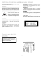
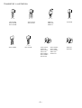
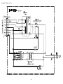
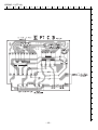
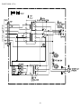
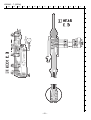
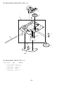
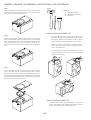
XR-M171 XR-M191 U U,LH SERVICE MANUAL COMPACT DISC STEREO SYSTEM BASIC CD MECHANISM : 3ZG-3 E2NC BASIC TAPE MECHANISM: BZM-1 AR2NC SYSTEM CD CASSEIVER SPEAKER XR–M171 CX–LM171 SX–LM171 XR–M191 CX–LM191 SX–LM191 REMOTE CONTROLLER RC–AAT11 • This Service Manual is the “Revision Publishing” and replace “Simple Manual” XR-M171/191<U,LH>, (S/M Code No. 09-012-443-6T1). S/M Code No. 09-013-443-6R1 N O SI I V TA E R A D SPECIFICATIONS TUNER FM tuning range: 87.5 MHz to 108 MHz FM usable sensitivity(IHF): 13.2 dBf FM antenna terminals: 75 ohms (unbalanced) AM tuning range: 530 kHz to 1710 kHz (10 kHz step) 531 kHz to 1602 kHz (9 kHz step) AM usable sensitivity: 350 mV/m AM antenna: Loop antenna SPEAKERS SX-LM171 (only for XR-M171) Speaker system: 2 way, bass reflex Speaker units: Woofer: 120 mm (4.7 in.) cone Tweeter: 20 mm (0.78 in.) cone Impedance: 16 ohms Dimensions (W x H x D): 144 x 255 x 204 mm ( 5.7 x 10 x 8 in.) Weight: 1.0 kg (2 lbs 3 oz) AMPLIFIER XR-M171 Power output: SPEAKERS SX-LM191 (only for XR-M191) Speaker system: 2 way, bass reflex Speaker units: Woofer: 120 mm (4.7 in.) cone Tweeter: 20 mm (0.78 in.) cone Impedance: 8 ohms Dimensions (W x H x D): 144 x 255 x 204 mm ( 5.7 x 10 x 8 in.) Weight: 1.5 kg (3 lbs 5 oz) 8 W + 8 W (50 Hz - 20 kHz, THD less than 1%, 16 ohms) 10 W + 10 W (1 kHz, THD less than 10%, 16 ohms) Total harmonic distortion: 0.2% (6 W, 1 kHz, 16 ohms, DIN AUDIO) XR-M191<U> Power output: 12 W + 12 W (50 Hz - 20 kHz, THD less than 1%, 8 ohms) 15 W + 15 W (1 kHz, THD less than 10%, 8 ohms) Total harmonic distortion: 0.2% (8 W, 1 kHz, 8 ohms, DIN AUDIO) XR-M191<LH> Power output: Rated: 12 W + 12 W (1 kHz, THD less than 1%, 8 ohms) Reference: 15 W + 15 W (1 kHz, THD less than 10%, 8 ohms) Total harmonic distortion: 0.2% (8 W, 1 kHz, 8 ohms, DIN AUDIO) Input: VIDEO/AUX: 0.4 V Output: SUB WOOFER: 500 mV SPEAKERS: 16 ohms or more<171> 8 ohms or more<191> PHONES: 32 ohms or more CASSETTE DECK Track format: Frequency response: Recording system: Heads: 4 tracks, 2 channels stereo 50 Hz - 15 kHz AC bias Recording/playback x 1, erase x 1 CD PLAYER Laser: D/A converter: Signal-to-noise ratio: Harmonic distortion: Semiconductor laser (l = 780 nm) 1 bit dual 75 dB (1 kHz, 0 dB) 0.2 % (1 kHz, 0 dB) GENERAL Power requirements: Power consumption: Power consumption in standby mode: With ECO mode on: 1.0 W With ECO mode off: 10 W Dimensions ( W x H x D): 167 x 255 x 240 mm (6.5 x 10 x 9.5 in.) Weight: 3.5 kg (7 lbs 12 oz) • Design and specifications are subject to change without notice. ACCESSORIES / PACKAGE LIST REF. NO. ! PART NO. 1 1 1 2 3 KANRI NO. 8B-CL9-901-010 8B-CL9-906-010 8B-CLW-901-010 87-043-115-010 87-A90-054-010 IB,U (ESF)-C<191U> IB,LH (ESP)-C<191LH> IB,U (ESF)-C<171U> FEEDER-ANT,FM ANT,LOOP AM-CON C 4 5 8A-CLB-961-210 87-A91-017-010 RC UNIT,RC-AAT11 PLUG,CONVERSION JT-0476<LH> 120 V AC, 60 Hz<U> 120 V/220 - 230 V/240 V AC (Switchable), 50 Hz/60Hz<LH> 35 W<171>, 45 W<191> DESCRIPTION –2– PROTECTION OF EYES FROM LASER BEAM DURING SERVICING This set employs laser. Therefore, be sure to follow carefully the instructions below when servicing. WARNING!! WHEN SERVICING, DO NOT APPROACH THE LASER EXIT WITH THE EYE TOO CLOSELY. IN CASE IT IS NECESSARY TO CONFIRM LASER BEAM EMISSION. BE SURE TO OBSERVE FROM A DISTANCE OF MORE THAN 30cm FROM THE SURFACE OF THE OBJECTIVE LENS ON THE OPTICAL PICK-UP BLOCK. CAUTION Use of controls or adjustments or performance of procedures other than those specified herin may result in hazardous radiation exposure. ATTENTION L’utillisation de commandes, réglages ou procédures autres que ceux spécifiés peut entraîner une dangereuse exposition aux radiations. ADVARSEL s Caution: Invisible laser radiation when open and interlocks defeated avoid exposure to beam. Advarsel: Usynlig laserståling ved åbning, når sikkerhedsafbrydere er ude af funktion. Undgå udsættelse for stråling. Usynlig laserståling ved åbning, når sikkerhedsafbrydereer ude af funktion. Undgå udsættelse for stråling. This Compact Disc player is classified as a CLASS 1 LASER product. The CLASS 1 LASER PRODUCT label is located on the rear exterior. VAROITUS! Laiteen Käyttäminen muulla kuin tässä käyttöohjeessa mainitulla tavalla saataa altistaa käyt-täjän turvallisuusluokan 1 ylittävälle näkymättömälle lasersäteilylle. CLASS 1 KLASSE 1 LUOKAN 1 KLASS 1 VARNING! Om apparaten används på annat sätt än vad som specificeras i denna bruksanvising, kan användaren utsättas för osynling laserstrålning, som överskrider gränsen för laserklass 1. LASER PRODUCT LASER PRODUKT LASER LAITE LASER APPARAT Precaution to replace Optical block (KSS-213F) Body or clothes electrostatic potential could ruin laser diode in the optical block. Be sure ground body and workbench, and use care the clothes do not touch the diode. PICK-UP ASSY PWB 1) After the connection, remove solder shown in right figure. Solder –3– ELECTRICAL MAIN PARTS LIST REF. NO. PART NO. KANRI NO. DESCRIPTION REF. NO. IC 87-020-454-010 87-A20-446-010 87-A21-319-010 87-A20-157-010 87-001-536-010 IC,DN6851 C-IC,LA9241ML C-IC,LC78622NE IC,TA2092N IC,NJM78M05FA 87-001-982-010 8B-CL9-631-010 87-A21-419-040 87-A21-831-010 87-A21-893-040 IC,TA7291S C-IC,LC866548A C-IC,NJM14558MD-TE2 IC,SPS-422-1-F1 C-IC,NJM14558V-TE2 87-A21-520-040 87-A21-695-010 87-A21-928-010 C-IC,M61509FP IC,LA1845L IC,LC72131D-N TRANSISTOR 87-A30-466-040 87-A30-436-040 89-109-521-080 89-318-155-080 87-026-610-080 C-TR,DTA144TKA C-TR,DTC144TKA TR,2SA952K TR,2SC1815GR TR,KTC3198GR 87-026-609-080 89-327-125-080 87-A30-196-080 87-A30-515-080 89-111-625-080 TR,KTA1266GR CHIP TR,2SC2712GR TR,2SC4115SRS TR,2SA1979O/Y C-TR,2SA1162GR 89-213-702-010 87-A30-455-040 87-A30-256-010 87-A30-255-010 87-026-219-080 TR,2SB1370E C-TR,DTA144EKA TR,2SD1933 TR,2SB1342 C-TR,DTA144ES (0.3W) 87-026-245-080 89-112-965-080 87-A30-087-080 87-A30-387-040 87-A30-074-080 C-TR,DTC114ES TR,2SA1296GR C-FET,2SK2158 C-TR,DTA124EUA C-TR,RT1P 141C 87-A30-234-080 89-327-143-080 87-A30-489-080 89-503-602-080 TR,CSC4115BC C-TR,2SC2714O C-TR,KRA107S C-FET,2SK360E 87-020-465-080 87-A40-270-080 87-A40-454-080 87-A40-748-080 87-A40-553-080 DIODE,1SS133 (110MA) C-DIODE,MC2838 DIODE,1N5393 GW ZENER,UZ5.6BSA DIODE,1N4003 LES 87-070-345-080 87-A40-781-080 87-A40-764-080 87-017-024-040 87-020-027-080 DIODE,IN4148 ZENER,UZ36BSA ZENER,UZ10BSC C-DIODE,DA204K CHIP-DIODE 1SS184 87-A40-739-080 87-017-149-080 ZENER,UZ2.7BSA AENER,HAS6A2L C101 C102 C104 C105 C106 87-A12-442-000 87-012-286-080 87-A12-381-000 87-A10-039-080 87-010-408-080 CAP,E 3300-25 M 85 IV LELON C-CAP,U 0.01-25 CAP,E 2200-25 M 85 IV LELON C-CAP,U 470P-50 J CH CAP, ELECT 47-50V C107 C108 C109 C110 C111 87-010-384-080 87-010-381-080 87-010-260-080 87-010-260-080 87-010-247-080 CAP, CAP, CAP, CAP, CAP, DIODE MAIN C.B ELECT ELECT ELECT ELECT ELECT 100-25V 330-16V 47-25V 47-25V 100-50V –4– PART NO. C112 C113 C114 C115 C116 KANRI NO. 87-010-263-080 87-010-403-080 87-010-374-080 87-A11-007-080 87-A11-007-080 DESCRIPTION CAP, ELECT 100-10V CAP, ELECT 3.3-50V CAP, ELECT 47-10V CAP,M 0.047-50 J DE CAP,M 0.047-50 J DE C122 C123 C131 C132 C133 87-010-260-080 87-010-260-080 87-A12-317-080 87-A12-317-080 87-012-286-080 CAP, ELECT 47-25V CAP, ELECT 47-25V C-CAP,U 0.1-50 Z F C-CAP,U 0.1-50 Z F C-CAP,U 0.01-25 C151 C200 C201 C207 C208 87-010-759-080 87-012-286-080 87-012-286-080 87-010-546-080 87-010-546-080 C-CAP,U, 0.1-25F C-CAP,U 0.01-25<191LH> C-CAP,U 0.01-25<191LH> CAP, ELECT 0.33-50V CAP, ELECT 0.33-50V C209 C210 C211 C212 C213 87-012-282-080 87-012-282-080 87-010-403-080 87-010-403-080 87-010-260-080 CAP, CAP, CAP, CAP, CAP, C214 C217 C218 C219 C220 87-010-260-080 87-010-959-080 87-010-959-080 87-010-759-080 87-010-759-080 CAP, ELECT 47-25V CHIP CAP,U 0.056-16F CHIP CAP,U 0.056-16F C-CAP,U, 0.1-25F C-CAP,U, 0.1-25F C227 C229 C230 C261 C273 87-010-260-080 87-012-199-080 87-012-199-080 87-012-286-080 87-010-759-080 CAP, ELECT 47-25V C-CAP,U 220P-50 C-CAP,U 220P-50 C-CAP,U 0.01-25 C-CAP,U, 0.1-25F<191LH> C303 C304 C305 C307 C308 87-A10-915-080 87-A10-915-080 87-010-246-080 87-010-263-080 87-010-263-080 C-CAP,U 1000P-25 J CH C-CAP,U 1000P-25 J CH CAP, ELECT 47-35V CAP, ELECT 100-10V CAP, ELECT 100-10V C313 C314 C315 C317 C318 87-012-280-080 87-012-280-080 87-010-374-080 87-010-546-080 87-010-546-080 C-CAP,U 3300P-50 C-CAP,U 3300P-50 CAP, ELECT 47-10V CAP, ELECT 0.33-50V CAP, ELECT 0.33-50V C340 C361 C362 C401 C402 87-012-199-080 87-010-374-080 87-010-401-080 87-010-401-080 87-010-401-080 C-CAP,U 220P-50 CAP, ELECT 47-10V CAP, ELECT 1-50V CAP, ELECT 1-50V CAP, ELECT 1-50V C403 C404 C405 C406 C407 87-012-193-080 87-012-193-080 87-012-284-080 87-012-284-080 87-010-784-080 C-CAP,U C-CAP,U C-CAP,U C-CAP,U C-CAP,U C408 C451 C452 C453 C454 87-010-784-080 87-010-787-080 87-010-248-080 87-012-279-080 87-012-279-080 C-CAP,U 0.012-25 B C-CAP,U 0.022-25 CAP, ELECT 220-10V C-CAP,U 2700P-50 B C-CAP,U 2700P-50 B C455 C456 C458 C459 C461 87-012-279-080 87-012-286-080 87-012-274-080 87-012-271-080 87-012-269-080 C-CAP,U 2700P-50 B C-CAP,U 0.01-25 CHIP CAP,U 1000P-50B C-CAP,U 560P-50 C-CAP,U 390P-50 B C462 C601 C602 C609 C610 87-012-269-080 87-012-276-080 87-012-276-080 87-012-287-080 87-010-785-080 C-CAP,U 390P-50 B CAP,CHIP U 1500P K B CAP,CHIP U 1500P K B C-CAP,U 0.015-25 F C-CAP,U 0.015-25 K B C611 C612 C613 C614 C615 87-010-545-080 87-010-545-080 87-010-545-080 87-010-545-080 87-012-172-080 CAP, ELECT 0.22-50V CAP, ELECT 0.22-50V CAP, ELECT 0.22-50V CAP, ELECT 0.22-50V CAPACITOR CHIP U 10P CH U 4700P-50 U 4700P-50 ELECT 3.3-50V ELECT 3.3-50V ELECT 47-25V 82P-50 CH 82P-50 CH 6800P-50 6800P-50 0.012-25 B REF. NO. PART NO. C616 C617 C619 C620 C627 KANRI NO. 87-010-408-080 87-010-408-080 87-010-401-080 87-010-401-080 87-012-286-080 DESCRIPTION CAP, ELECT 47-50V CAP, ELECT 47-50V CAP, ELECT 1-50V CAP, ELECT 1-50V C-CAP,U 0.01-25 C628 C635 C663 C697 C698 87-012-286-080 87-012-274-080 87-010-759-080 87-012-286-080 87-012-286-080 C915 C916 CN202 CN351 CN702 REF. NO. PART NO. PR301 PR301 S301 S302 S303 KANRI NO. 87-A91-957-080 87-026-689-080 87-A90-164-080 87-A90-164-080 87-A90-164-080 DESCRIPTION FUSE,630MA 125V F 20N<191U,171U> PROTECTOR,1A 491SERIES 60V<191LH> SW,TACT SKQNAB(N) SW,TACT SKQNAB(N) SW,TACT SKQNAB(N) C-CAP,U 0.01-25 CHIP CAP,U 1000P-50B<191LH> C-CAP,U, 0.1-25F C-CAP,U 0.01-25 C-CAP,U 0.01-25 S304 S305 S306 S307 S308 87-A90-164-080 87-A90-164-080 87-A90-164-080 87-A90-164-080 87-A90-164-080 SW,TACT SW,TACT SW,TACT SW,TACT SW,TACT SKQNAB(N) SKQNAB(N) SKQNAB(N) SKQNAB(N) SKQNAB(N) 87-012-336-080 87-012-336-080 87-099-719-010 87-A60-624-010 87-099-570-010 CAP,CHIP U 3300P SL CAP,CHIP U 3300P SL CONN,30P H BLK TYK-B(X) CONN,7P V 2MM JMT CONN,13P V TUC-P13P-B1 S309 S310 S311 S312 S313 87-A90-164-080 87-A90-164-080 87-A90-164-080 87-A90-164-080 87-A90-164-080 SW,TACT SW,TACT SW,TACT SW,TACT SW,TACT SKQNAB(N) SKQNAB(N) SKQNAB(N) SKQNAB(N) SKQNAB(N) CNA101 FB401 FB402 FB601 FB603 8A-NF8-655-010 83-XM1-617-080 83-XM1-617-080 87-A90-896-080 87-A90-896-080 CONN ASSY,7P TID-A(150) C-COIL,BK2125HM601 C-COIL,BK2125HM601 F-BEAD, 035600STY7 F-BEAD, 035600STY7 S314 S315 S316 S317 S318 87-A90-164-080 87-A90-164-080 87-A90-164-080 87-A90-164-080 87-A90-164-080 SW,TACT SW,TACT SW,TACT SW,TACT SW,TACT SKQNAB(N) SKQNAB(N) SKQNAB(N) SKQNAB(N) SKQNAB(N) FB606 J231 J241 J601 J603 83-XM1-617-080 87-A60-420-010 87-A60-217-010 87-A60-881-010 87-099-801-010 C-COIL,BK2125HM601 JACK,3.5 ST (MSC) TERMINAL,SPKR 4P JACK,PIN 2P MSP 242V05 PBSN JACK,PIN 1P BLK W/O SW S320 S351 X301 87-A90-164-080 87-A91-690-010 87-A70-070-080 SW,TACT SKQNAB(N) SW,RTRY JOG RE0121PVB25FINB VIB,CER 5.76MHZ CRHF L201 L202 L451 PN101 R223 87-A50-610-010 87-A50-610-010 87-007-342-010 87-A90-460-010 87-A00-258-080 COIL,1UH K(MDEC) COIL,1UH K(MDEC) COIL,OSC 85KHZ BIAS HLDR,WIRE 2.5-7P RES,M/F 0.22-1W J R224 R249 R250 87-A00-258-080 87-A00-258-080 87-A00-258-080 RES,M/F 0.22-1W J RES,M/F 0.22-1W J RES,M/F 0.22-1W J C1 C2 C3 C4 C5 87-010-403-080 87-012-286-080 87-010-263-080 87-010-248-080 87-012-286-080 CAP, ELECT 3.3-50V C-CAP,U 0.01-25 CAP, ELECT 100-10V CAP, ELECT 220-10V C-CAP,U 0.01-25 C6 C7 C8 C9 C10 87-010-374-080 87-012-274-080 87-010-787-080 87-010-263-080 87-010-263-080 CAP, ELECT 47-10V CHIP CAP,U 1000P-50B C-CAP,U 0.022-25 CAP, ELECT 100-10V CAP, ELECT 100-10V C102 C103 C106 C302 C304 87-012-278-080 87-010-264-040 87-010-263-040 87-012-286-080 87-010-405-040 C-CAP,U 2200P-50 B CAP,E 100-10 5L CAP,E 100-10 C-CAP,U 0.01-25 CAP,E 10-50 C12 C13 C14 C16 C17 87-010-401-080 87-012-286-080 87-010-405-080 87-010-545-080 87-012-274-080 CAP, ELECT 1-50V C-CAP,U 0.01-25 CAP, ELECT 10-50V CAP, ELECT 0.22-50V CHIP CAP,U 1000P-50B C307 C308 C309 C314 C315 87-010-421-040 87-010-421-040 87-010-787-080 87-010-370-040 87-A10-025-080 CAP,E 4.7-50 5L CAP,E 4.7-50 5L C-CAP,U 0.022-25 CAP,E 330-6.3 SME C-CAP,U 0.22-16 Z F C18 C20 C22 C23 C29 87-010-785-080 87-010-788-080 87-012-276-080 87-010-757-080 87-012-282-080 C-CAP,U C-CAP,U C-CAP,U C-CAP,U C-CAP,U C317 C329 C330 C331 C333 87-010-787-080 87-010-787-080 87-A11-084-080 87-018-149-080 87-015-694-040 C-CAP,U 0.022-25 C-CAP,U 0.022-25 CAP,TC U 68P-50 J CH CAP,TC U 15P-50 CH CAP,E 0.47-50 C30 C31 C32 C33 C34 87-012-199-080 87-010-545-080 87-010-374-080 87-010-401-080 87-012-278-080 C-CAP,U 220P CAP, ELECT 0.22-50V CAP, ELECT 47-10V CAP, ELECT 1-50V C-CAP,U 2200P-50 B C335 C338 C339 C340 C420 87-018-113-080 87-012-286-080 87-012-286-080 87-012-286-080 87-010-759-080 CAP,TC U 33P-50V C-CAP,U 0.01-25 C-CAP,U 0.01-25 C-CAP,U 0.01-25 C-CAP,U, 0.1-25F C35 C36 C37 C38 C39 87-012-286-080 87-010-374-080 87-010-404-080 87-010-759-080 87-012-274-080 C-CAP,U 0.01-25 CAP, ELECT 47-10V CAP, ELECT 4.7-50V C-CAP,U, 0.1-25F CHIP CAP,U 1000P-50B C421 C422 C423 CN4 CN301 87-012-188-080 87-012-286-080 87-010-403-040 87-099-032-010 87-099-720-010 C-CAP,U 47P-50 CH C-CAP,U 0.01-25 CAP,E 3.3-50 SME CONN,15P H BLK 6216 CONN,30P BLK TYK-B(P) C40 C42 C43 C45 C46 87-012-162-080 87-012-172-080 87-018-174-080 87-010-759-080 87-010-759-080 C-CAP,U 1P-50 CK CAPACITOR CHIP U 10P CH CAP, TC U 18P C-CAP,U, 0.1-25F C-CAP,U, 0.1-25F CN302 FFC302 FFC4 FL301 LED301 87-A60-079-010 88-908-151-210 88-915-231-110 8A-CL9-684-010 87-A40-229-040 CONN,08P H 9604S-08F FF-CABLE,8P 1.25-150MM FF-CABLE,15P 1.25 230MM FL,HNA-11SS 29T LED,SLR-342VR TB7 RED C47 C48 C50 C51 C57 87-010-759-080 87-012-182-080 87-A10-039-080 87-A12-309-080 89-654-255-080 C-CAP,U, 0.1-25F C-CAP,U 27P-50 CH C-CAP,U 470P-50 J CH C-CAP,U 680P-50 J CH CAP,TC 33P-50 J CH UP125 LED302 LED303 LED304 LED305 87-A40-619-040 87-A40-619-040 87-A40-619-040 87-A40-619-040 LED,SLR-56PT-T31-W LED,SLR-56PT-T31-W LED,SLR-56PT-T31-W LED,SLR-56PT-T31-W C58 C59 C60 C61 89-654-255-080 87-010-263-080 87-010-759-080 87-010-759-080 CAP,TC 33P-50 J CH UP125 CAP, ELECT 100-10V C-CAP,U, 0.1-25F C-CAP,U, 0.1-25F CD C.B FRONT C.B GRN GRN GRN GRN –5– 0.015-25 K B 0.033-25 1500P 0.047-25F 4700P-50 REF. NO. PART NO. C62 C65 C66 C67 C75 KANRI NO. 87-010-370-080 87-010-404-080 87-010-759-080 87-010-263-080 87-012-286-080 DESCRIPTION CAP,E 330-6.3 SME CAP, ELECT 4.7-50V C-CAP,U, 0.1-25F CAP, ELECT 100-10V C-CAP,U 0.01-25 C76 C77 C78 C79 C80 87-A10-102-080 87-010-263-080 87-012-286-080 87-012-286-080 87-010-112-080 C81 C82 C83 C84 C90 REF. NO. C784 C785 C786 C788 C789 KANRI NO. 87-012-286-080 87-012-286-080 87-010-787-080 87-012-167-080 87-010-787-080 C-CAP,U C-CAP,U C-CAP,U C-CAP,U C-CAP,U CAP,E 1000-10 REA CAP, ELECT 100-10V C-CAP,U 0.01-25 C-CAP,U 0.01-25 CAP, ELECT 100-16V C790 C791 C792 C793 C795 87-010-787-080 87-010-831-080 87-012-286-080 87-A11-056-080 87-012-286-080 C-CAP,U 0.022-25 K B C-CAP,U,0.1-16F C-CAP,U 0.01-25 K B C-CAP,U 1-10 Z F C-CAP,U 0.01-25 K B 87-010-405-080 87-010-405-080 87-012-277-080 87-012-277-080 87-012-286-080 CAP, ELECT 10-50V CAP, ELECT 10-50V C-CAP,U 1800P-50 B C-CAP,U 1800P-50 B C-CAP,U 0.01-25 C799 C801 C802 C804 C807 87-010-982-040 87-A11-056-080 87-010-829-080 87-010-555-040 87-A10-463-080 CAP,E 33-25 GAS C-CAP,U 1-10 Z F CAP, U 0.047-16 CAP,E 100-10 GAS C-CAP,U,0.47-10 Z F C91 C92 C93 C94 C95 87-010-405-080 87-010-387-080 87-012-286-080 87-012-286-080 87-012-286-080 CAP, ELECT 10-50V CAP,E 470-25 SME C-CAP,U 0.01-25 C-CAP,U 0.01-25 C-CAP,U 0.01-25 C808 C809 C810 C814 C815 87-A11-056-080 87-A11-056-080 87-010-831-080 87-012-286-080 87-A10-463-080 C-CAP,U 1-10 Z F C-CAP,U 1-10 Z F C-CAP,U,0.1-16F C-CAP,U 0.01-25 K B C-CAP,U,0.47-10 Z F C96 C97 C98 C100 C101 87-010-221-080 87-012-286-080 87-012-197-080 87-012-278-080 87-012-195-080 CAP, ELECT 470-10V C-CAP,U 0.01-25 C-CAP,U 150P-50 CH C-CAP,U 2200P-50 B C-CAP,U 100P-50CH C816 C821 C823 C824 C825 87-A10-463-080 87-A11-063-080 87-012-273-080 87-A11-063-080 87-A11-317-080 C-CAP,U,0.47-10 Z F C-CAP,S 4.7-10 Z F C-CAP,U 820P-50 K B C-CAP,S 4.7-10 Z F C-CAP,U 0.068U-16 K B C102 C103 C104 C105 C110 87-012-195-080 87-012-195-080 87-012-195-080 87-012-195-080 87-010-759-080 C-CAP,U 100P-50CH C-CAP,U 100P-50CH C-CAP,U 100P-50CH C-CAP,U 100P-50CH C-CAP,U, 0.1-25F C831 C836 C842 C844 C850 87-010-552-040 87-012-286-080 87-012-286-080 87-012-286-080 87-A11-056-080 CAP,E 22-16 GAS C-CAP,U 0.01-25 K B C-CAP,U 0.01-25 K B C-CAP,U 0.01-25 K B C-CAP,U 1-10 Z F C162 CN1 CN3 CN4 CN6 87-012-274-080 87-A60-424-010 87-A60-131-010 87-099-032-010 87-A60-153-010 CHIP CAP,U 1000P-50B CONN,16P V TOC-B CONN,6P V FE CONN,15P H BLK 6216 CONN,5P H FE C851 C852 C853 C858 C860 87-012-286-080 87-012-286-080 87-012-286-080 87-010-831-080 87-012-286-080 C-CAP,U C-CAP,U C-CAP,U C-CAP,U C-CAP,U 0.01-25 K B 0.01-25 K B 0.01-25 K B 0.1-16 Z F 0.01-25 K B FFC1 FFC3 FFC6 R70 R73 88-CL4-704-010 88-906-131-110 88-905-231-110 87-029-019-090 87-029-361-090 FF-CABLE, 16P 1.0 FF-CABLE,6P 1.25 FF-CABLE, 5P 1.25 230MM RES,FUSE 2.2-1/2W J RES,FUSE 3.3-1/2W J C902 C908 C909 C911 C912 87-012-167-080 87-012-176-080 87-012-274-080 87-012-170-080 87-012-195-080 C-CAP,U C-CAP,U C-CAP,U C-CAP,U C-CAP,U 5P-50 C CH 15P-50 J CH 1000P-50 K B 8P-50 D CH 100P-50CH R85 R86 R87 R88 R107 87-022-284-080 87-022-284-080 87-022-284-080 87-022-284-080 87-022-243-080 C-RES,U 68K-1/16W F C-RES,U 68K-1/16W F C-RES,U 68K 1-16W F C-RES,U 68K 1-16W F CHIP RES,U 15K-1/16W F C913 C914 C915 C918 C920 86-ZA1-616-080 86-ZA1-616-080 86-ZA1-616-080 87-012-164-080 87-012-180-080 C-CAP,U C-CAP,U C-CAP,U C-CAP,U C-CAP,U 0.01-50 K B (MUR) 0.01-50 K B (MUR) 0.01-50 K B (MUR) 2P-50 C CH 22P-50 J CH R108 R109 R110 X1 87-022-243-080 87-022-243-080 87-022-243-080 87-A70-046-010 CHIP RES,U 15K-1/16W F CHIP RES,U 15K-1/16W F CHIP RES,U 15K-1/16W F VIB,XTAL 16.934MHZ C921 C922 C923 C924 C927 87-012-186-080 87-012-174-080 87-012-270-080 87-012-174-080 87-012-195-080 C-CAP,U 39P-50 J CH CAP CHIP CERA SS 12P CHJ C-CAP,U 470P-50 K B C-CAP,U 12P-50 J CH C-CAP,U 100P-50CH C961 C963 C971 C972 C973 87-012-170-080 87-010-831-080 87-010-381-080 87-A11-063-080 87-012-286-080 C-CAP,U 8P-50 D CH C-CAP,U,0.1-16F CAP, ELECT 330-16V C-CAP,S 4.7-10 Z F C-CAP,U 0.01-25 K B C974 C976 C979 C981 C982 87-012-286-080 87-010-831-080 87-012-195-080 87-010-553-040 87-010-831-080 C-CAP,U 0.01-25 K B C-CAP,U,0.1-16F C-CAP,U 100P-50CH CAP,E 47-16 GAS C-CAP,U,0.1-16F C983 C984 C985 C987 C990 87-A11-132-080 87-012-286-080 87-012-195-080 87-012-286-080 87-012-195-080 CAP,TC U 0.01-50 K B C-CAP,U 0.01-25 K B C-CAP,U 100P-50CH C-CAP,U 0.01-25 K B C-CAP,U 100P-50CH C991 C992 C993 C994 C995 87-012-176-080 87-012-176-080 87-012-274-080 87-012-195-080 87-012-274-080 C-CAP,U 15P-50 C-CAP,U 15P-50 CHIP CAP,U 1000P-50B C-CAP,U 100P-50CH CHIP CAP,U 1000P-50B PT C.B ! ! ! ! ! ! ! ! ! ! ! ! C101 CN101 F101 FC101 FC102 87-010-387-080 87-A61-109-010 87-035-454-010 87-033-213-080 87-033-213-080 CAP,E 470-25 SME CONN,7P V TID-A FUSE,1.6A 250V T 218<191LH> FUSE CLAMP, PFC5000<191LH> FUSE CLAMP, PFC5000<191LH> PT101 PT101 PT102 PT102 RY102 8B-CL9-644-010 8B-CL9-642-010 8B-NF9-663-010 8B-NF9-661-010 87-A91-281-010 PT,LH<191LH> PT,U<191U,171U> PT,SUB BNF H (TAM)<191LH> PT,SUB BNF U (TAM)<191U,171U> RELAY,AC DC12V OSA-SS-212DM5<191LH> RY102 SW101 T101 T102 87-A90-976-010 87-A90-234-010 87-A60-317-010 87-A60-317-010 RELAY,AC12V SDT-S-112LMR<191U,171U> SW,SL 1-2-2 SWS2201<191LH> TERMINAL, 1P MSC TERMINAL, 1P MSC 87-012-286-080 C-CAP,U 0.01-25 K B TUNER C.B C772 –6– PART NO. DESCRIPTION 0.01-25 K B 0.01-25 K B 0.022-25 K B 5P-50 CH 0.022-25 K B REF. NO. PART NO. C996 C997 C998 C999 CF831 KANRI NO. 87-012-195-080 87-010-831-080 87-010-553-040 87-012-286-080 87-008-261-010 DESCRIPTION REF. NO. C-CAP,U 100P-50CH C-CAP,U,0.1-16F CAP,E 47-16 GAS C-CAP,U 0.01-25 K B FLTR,CF SFE10.7MA5 CF832 CN991 D902 D903 J832 87-008-261-010 87-A60-700-010 87-A40-916-040 87-A40-916-040 87-A61-535-010 FLTR,CF SFE10.7MA5 CONN,13P H GRY TUC-P13X-C1 C-VARI-CAP,HVC202A C-VARI-CAP,HVC202A TERMINAL,ANT 2P HSP-302V J940 L801 L802 L811 L832 87-A60-633-010 87-A50-694-010 87-A91-551-010 87-005-847-080 87-005-847-080 CONN,2P H 2.5MM JMT COIL,FM-DET 2 (COILS) FLTR,PCFJZH-450 L(TOK) COIL,2.2UH CECS COIL,2.2UH CECS L903 L904 L906 L907 L908 88-ZA1-602-110 88-ZA1-601-010 87-005-847-080 8A-NEC-611-010 88-ZA1-624-010 COIL,FM-RF-U2 2G COIL,FM-RF-U1 2G COIL,2.2UH CECS COIL,FM OSC U 2G COIL,FM IFT 7-6.2 (COILS) L951 R790 R902 X991 8A-NF8-667-010 87-012-286-080 87-012-166-080 87-A70-061-010 COIL,AM PACK 4(TOK) CAP, U 0.01-25 C-CAP,U 4P-50 C CH VIB,XTAL 4.500MHZ CSA-309 87-A60-086-010 87-045-358-010 87-045-356-010 87-A90-042-010 CONN,6P H 6216 MOT,RF-310TA 43 MOT,RF-310TA 30 SW,LEAF MSW-17310MVP0 PART NO. KANRI NO. DESCRIPTION LOAD C.B CON6 M1 SW1 SW2 87-099-210-010 87-045-305-010 87-036-110-010 87-036-110-010 CONN,5P 6216 H MOTOR, RF-500TB DC-5V (2MA) PUSH SWITCH PUSH SWITCH CN1 M1 SOL2 SW1 SW2 87-A60-079-010 87-A91-825-010 82-ZM3-628-010 87-036-110-010 87-036-110-010 CONN,08P H 9604S-08F MOT,M09Y/Z SOL ASSY,23 SO SW,MICRO SPPB62 SW,MICRO SPPB62 SW4 SW5 87-036-110-010 87-036-110-010 SW,MICRO SPPB62 SW,MICRO SPPB62 85-ZM3-602-010 88-CL4-701-010 PWB,FLEX A CONN ASSY,7P RPEH DECK C.B HEAD C.B CON351 DRIVE C.B CON3 M20 M21 SW1 CHIP RESISTOR PART CODE Chip Resistor Part Coding 8 8 A Figure Resistor Code Value of resistor Chip resistor L W t :A Resistor Code : A 1.0 0.5 0.35 104 1.6 0.8 0.45 108 2 1.25 0.45 118 3.2 1.6 0.55 128 Dimensions (mm) Wattage 1/16W Type 1005 Tolerance 5% Symbol CJ 1/16W 1/10W 1608 2125 5% 5% CJ CJ 1/8W 3216 5% CJ –7– Form L t W TRANSISTOR ILLUSTRATION E C B CSC4115BC KTA1266GR KTC3198GR B C E 2SA1979O/Y 2SC1815GR B C E E C B 2SB1342 2SB1370E 2SD1933 2SA952K D C B E C B E C B 2SC4115SRS 2SA1296GR 2SA1162GR 2SA1235F 2SC2712GR 2SC2714O DTA124EUA DTA144EKA DTA114ES –8– G E DTA144TKA DTC114ES DTC144TKA KRA107S RT1P141C S 2SK2158 2SK360E WIRING 1 (MAIN) 32 31 30 29 28 27 26 25 24 23 22 21 20 19 18 17 16 15 14 13 12 11 10 9 8 7 6 5 4 3 2 1 A B C D E F G H I J K L M N O P Q R S T U 9 SCHEMATIC DIAGRAM – 1 (MAIN) – 10 – WIRING 2 (TUNER) 15 14 13 12 11 10 9 8 7 6 5 4 3 2 1 A B C D E F G H I J K L M N O P Q R S T U 11 SCHEMATIC DIAGRAM – 2 (TUNER) – 12 – WIRING 3 (FRONT) 32 31 30 29 28 27 26 25 24 23 22 21 20 19 18 17 16 15 14 13 12 11 10 9 8 7 6 5 4 3 2 1 A B C D E F G H I J K L M N O P Q R , , , S , T U 13 SCHEMATIC DIAGRAM – 3 (FRONT / DECK) – 14 – WIRING 4 (CD / DRIVE / LOAD) 32 31 30 29 28 27 26 25 24 23 22 21 20 19 18 17 16 15 14 13 12 11 10 9 8 7 6 5 4 3 2 1 A B C D E F G H I J K L M N O P Q R S T U 15 SCHEMATIC DIAGRAM – 4 (CD / DRIVE / LOAD) – 16 – WIRING 5 (PT: U) 15 14 13 12 11 10 9 8 7 6 5 4 3 2 1 A B C D E F G H I J K L M N O P Q R S T U 17 SCHEMATIC DIAGRAM – 5 (PT: U) – 18 – WIRING 6 (PT: LH) 15 14 13 12 11 10 9 8 7 6 5 4 3 2 1 A B C D E F G H I J K L M N O P Q R S T U 19 SCHEMATIC DIAGRAM – 6 (PT: LH) – 20 – WIRING 7 (DECK) 15 14 13 12 11 10 9 8 7 6 5 4 3 2 1 A B C D E F G H I J K L M N O P Q R S T U 21 IC BLOCK DIAGRAM – 22 – FL (HNA-11SS 29T) GRID ASSIGNMENT AND ANODE CONNECTION GRID ASSIGNMENT – 23 – ANODE CONNECTION – 24 – IC DESCRIPTION IC, LC866548A Description Pin No. Pin Name I/O 1 I-ST/MO I Tuner stereo input. 2 I-TU/IFC I Tuner TUNE IFC input. 3 O-SOL O Deck solenoid ON/OFF output. 4 O-REC/PB O Deck record/playback select output. 5 O-MOTOR O Deck motor ON/OFF control output. 6 O-BIAS O Record 85 kHz oscillaor ON/OFF output. 7 O-MUTE O Mute output. 8 O-TU_ON O Tuner mode on output. 9 O-POWER O Power ON/OFF control output. 10 O-CLK_SHIFT O Micon clock shift output. 11 O-PLL_CE O PLL chip enable output. 12 I-RESET I Micon reset input. 13 XCIN I Connected to VDD1. 14 XCOUT O Not used. 15 VSS1 - Digital GND. 16 XIN I 17 XOUT O 18 VDD1 - Power supply. 19 I-VOL I Rotary encoder volume A/D input. 20 I-HOLD I System hold input A/D input. 21 I-SW_TP I Cassette detect switch A/D input. 22 I-KEY2 I Key2 A/D input. 23 I-KEY1 I Key1 A/D input. 24 I-CDTSW I CD tray switch A/D input. 25 I-RDS_SIG I RDS tuning level input. (Not used) 26 I-CD_SIG I CD music level input. 27 I-TMBASE I Time base clock base (8 Hz) input. 28 I-RDCL I RDS clock input. (Not used) 29 I-RMC I Remote control data input. 30 ~ 33 NC - Not connected. 34 ~ 44 O-G1 ~ G11 O FL grid G1 ~ G11 output. 45 O-P1 O FL port P1 output. 46 VDD3 - Power supply. 47 ~ 50 O-P2 ~ P5 O FL port P2 ~ P5 output. 51 VEE - Power supply. 52 ~ 68 O-P6 ~ P22 O FL port P6 ~ P22 output. 69 I-AM10K I AM10K detect input. (Not used) 59 I-OIRT I OIRT detect input. (Not used) 60 I-RDS I RDS detect input. (Not used) 61 VDD4 - Power supply. 62 I-AMST I AM stereo detect input. (Not used) 5.76 MHz Ceralock. – 25 – Description Pin No. Pin Name I/O 74 I-LW I LW detect input. (Not used) 75 I-SW I SW detect input. (Not used) 76 I-STOP I Deck stop signal input. 77 I-AS I Auto stop signal input. 78 I-WRQ I CD WRQ input. 79 I-DRF I CD DRF input. 80 NC - Not connected. 81 O-CD_ON O CD ON/OFF control output. 82 O-CD_CLOSE O CD tray close output. 83 O-CD_OPEN O CD tray open output. 84 NC - Not connected. 85 O-LED_TP O Tape function LED ON/OFF output. 86 O-LED_CD O CD function LED ON/OFF output. 87 O-LED_AUX O Aux function LED ON/OFF output. 88 O-LED_TU O Tuner functon LED ON/OFF output. 89 AVSS - Connected to GND. 90 VDD2 - Power supply. 91 O-CLK O Common serial clock output. 92 O-ECO_LED O Economical mode LED ON/OFF output. 93 O-RECMUTE O Record mute output. 94 O-ECO O Economical mode ON/OFF output. 95 O-RWC O CD control data output. 96 I-SQOUT I CD SQOUT input. 97 O-CQCK O CD clock output. 98 O-DATA O Line out mute output. 99 O-COIN O Command to CD DSP output. 100 I-RDDA I RDS data input. (Not used) – 26 – IC, LA9241ML Pin No. Pin Name I/O Description 1 FIN2 I 2 FIN1 I 3 E I 4 F I Connects to the pickup's photo diode. 5 TB I Input for DC component of TE signal. 6 TE– I Connects to the resistor between this pin and TE pin for setting the gain of TE signal. 7 TE O Output for TE signal. 8 TESI I Input for TES (Track Error Sense) comparator, TE signal is band-passed and inputted. 9 SCI I Input for shock detection. 10 TH I For setting tracking gain time constant. 11 TA O TA amplifier output pin. 12 TD– I For constructing tracking phase compensation constant between TD and VR pins. 13 TD O For setting tracking phase compensation. 14 JP I For setting the amplifier of tracking jump signal (kick pulse). 15 TO O Output for tracking control signal. 16 FD O Output for focusing control signal. 17 FD– I For constructing focusing phase compensation constant between FD and FA pins. 18 FA O For constructing focusing phase compensation constant between FD– and FA– pins. 19 FA– I For constructing focusing phase compensation constant between FA and FE pins. 20 FE O Output for FE signal. 21 FE– I Connects to the gain-setting resistor of FE signal between this pin and FE pin. 22 A-GND – GND for analog signals. 23 SP 24 SPI O Single end output of CV+ and CV– pin input signal. 25 SPG I Connects to the gain-setting resistor during spindle 12cm mode. 26 SP– I Connects to spindle phase compensation constant together with SPD pin. 27 SPD O Output for spindle control signal. 28 SLEQ I Connects to sled phase compensation constant. 29 SLD O Output for sled control signal. 30 SL– I Input for sled-sending signal from microcontroller. 31 SL+ I Input for sled-sending signal. 32 JP– I Input for tracking-jump signal from DSP. 33 JP+ 34 TGL I Input for tracking gain control signal from DSP; gain is low if TGL = "H". 35 TOFF I Input for tracking off control signal from DSP; off if TOFF = "H". 36 TES O Outputs TES signal to DSP. 37 HFL O 38 SLOF I Connects to the pickup's photo diode; adding this pin to pin FIN1 generates RF signal, and subtracting it generates FE signal. Connects to the pickup's photo diode. Connects to the pickup's photo diode; subtracting this pin from pin F generates TE signal. HIGH FREQUENCY LEVEL; used to determine whether the main beam is on a pit or on a mirror. Input for sled servo off control. – 27 – Pin No. Pin Name 39 CV– 40 CV+ 41 I/O Description I Input for CLV error signal from DSP. RFSM O Output for RF. 42 RFS– O For setting RF gain and 3T compensation constant together with RFSM. 43 SLC O 44 SLI I Input for controlling the data slice level of DSP. 45 D-GND – GND for digital system. 46 FSC O Output pin for focus search smoothing capacitor. 47 TBC I (Tracking Balance Control) EF balance variable range setting pin. 48 NC – Not connected. 49 DEF O Output for disk defect detection. 50 CLK I Standard clock input; DSP's 4.23MHz is inputted. 51 CL I Clock input for microcontroller command. 52 DAT I Data input for microcontroller command. 53 CE I Chip-enable input for microcontroller command. 54 DRF O Detect RF; output for RF level detection. 55 FSS I 56 VCC2 – VCC pin for servo and digital systems. 57 REFI I For connecting pass capacitor to reference voltage. 58 VR O Reference voltage output. 59 LF2 – For setting disk defect-detection time constant. 60 PHI – Connects to capacitor for RF signal peak hold. 61 BHI – Connects to capacitor for RF signal bottom hold. 62 LDD O Output for APC circuit. 63 LDS I Input for APC circuit. 64 VCC1 – VCC pin for RF system. SLICE LEVEL CONTROL; output for controlling the data slice level of DSP with RF waveform. (Focus Search Mode) = search/+search against reference voltage switching pin. (Not used) – 28 – IC, LC78622NE Pin No. Pin Name I/O 1 DEFI I Defect detection signal (DEF) input. 2 TAI I Test input. A pull-down resistor is built in. Must be connected to 0V. 3 PDO O External VCO control phase comparator output. 4 VVSS – Internal VCO ground. Must be connected to 0V. 5 ISET O PDO output current adjustment resistor connection. 6 VVDD – Internal VCO power supply. 7 FR – VCO frequency range adjustment. 8 VSS – Digital system ground. Must be connected to 0V. 9 EFMO O Slice level control; EFM signal output. 10 EFMIN I Slice level control; EFM signal input. 11 T2 I Test input. A pull-down resistor is built in. Must be connected to 0V. 12 CLV+ O Description Disc motor control output. Three-value ouput is also possible when specified by microprocessor command. 13 CLV– 14 V/P O 15 HFL I Track detection signal input. This is a Schmitt input. 16 TES I Tracking error signal input. This is a Schmitt input. 17 TOFF O Tracking off output. 18 TGL O Tracking gain switching output. Increase the gain when low. 19 JP+ O 20 JP– 21 PCK O Rough servo/phase control automatic switching monitor output. Outputs a high level during rough servo and a low level during phase control. Track jump output. Three-value output is also possible when specified by microprocessor command. EFM data playback clock monitor. Outputs 4.3218 MHz when the phase is locked. (Not used) Synchronization signal detection ouput. Outputs a high level when the synchronization 22 FSEQ O signal detected from the EFM signal and the internally generated synchronization signal agree. (Not used) 23 VDD – Digital system power supply. 24 SL+ 25 SL– O Serial data command sled signal output terminal from microprocessor. 26 NC – Not used. 27 PU IN I CD pickup inside limit switch. 28 CD R/W O CD R/W gain ON/OFF signal. 29 EMPH O 30 C2F O C2 flag output. (Not used) 31 DOUT O Digital output (EIAJ format). (Not used) 32 T3 I Test input. A pull-down resistor is built in. Must be connected to 0V. 33 T4 34 NC – Not connected. 35 MUTEL O Left channel one-bit D/A converter mute output. 36 LVDD – Left channel one-bit D/A converter power supply. De-emphasis monitor pin. A high level indicates playback of a de-emphasis disk. (Not used) – 29 – Pin No. Pin Name I/O Description 37 LCHO O Left channel one-bit D/A converter output. 38 LVSS – Left channel one-bit D/A converter ground. (Must be connected to 0V) 39 RVSS – Right channel one-bit D/A converter ground. (Must be connected to 0V) 40 RCHO O Right channel one-bit D/A converter output. 41 RVDD – Right channel one-bit D/A converter power supply. 42 MUTER O Right channel one-bit D/A converter mute ouput. 43 XVDD – Crystal oscillator power supply. 44 XOUT O 45 XIN I 46 XVSS – Crystal oscillator ground. Must be connected to 0V. 47 SBSY O Subcode block synchronization signal output. (Not used) 48 EFLG O C1, C2 single and double error correction monitor pin. (Not used) 49 PW O Subcode P, Q, R, S, T, U, V and W output. (Not used) 50 SFSY O 51 SBCK I 52 FSX O 53 WRQ O Subcode Q output standby output. 54 RWC I Readwrite control input. This is a Schmitt input. 55 SQOUT O Subcode Q output. 56 COIN I Command input from the control microprocessor. 57 CQCK I 58 RES I Chip reset pin. (This pin must be set low briefly after power is first applied) 59 T11 O Test output. Leave open. (Normally outputs a low level). (Not used) 60 16M O 16.9344 MHz output. (Not used) 61 4.2M O 4.2336 MHz output. 62 T5 I Test input. A pull-down resistor is built in. (Must be connected to 0V) 63 CS I 64 T1 I Connections for a 16.934MHz crystal oscillator element. Subcode frame synchronization signal output. This signal falls when the subcode are in the standby state. (Not used) Subcode readout clock input. This is a Schmitt input. (Must be connected to 0V when unused) Output for the 7.35 kHz synchronization signal divided from the crystal oscillator. (Not used) Input for both the command input acquisition clock and the SQOUT pin subcode readout clock input. This is a Schmitt input. Chip select input. A pull-down resistor is built in. Must be connected to 0V if not controlled. Test input. No pull-down resistor. (Must be connected to 0V) – 30 – ADJUSTMENT <TUNER / DECK> < TUNER SECTION > 1. Clock Frequency Check Settings : • Test point : TP2 (CLK) Method : Set to AM 1710 kHz and check that the test point is 2160 kHz ± 45 Hz. 11. FM Separation Check Settings : • Test point : TP8 (Rch), TP9 (Lch) • Input level : 60 dBµV Method : Set to FM 98.0 MHz and check that the separation more than 25 dB. 2. AM VT Check Settings : • Test point : TP1 (VT) Method : Set to AM 1710 kHz and check that the test point is less than 8.5 V. Then set to AM 530 kHz and check that the test point is more than 0.6 V. 3. AM Tracking Adjustment Settings : • Test point : TP8 (Rch), TP9 (Lch) • Adjustment location : L951(1/3) Method : Set to AM 1000 kHz and adjust L951(1/3) so that the test point becomes maximum. < DECK SECTION > 1. Tape Speed Check Settings : • Test tape : TTA–100 • Test point : SP OUT Method : Play back the test tape and check the test point is 3000 Hz ± 5 Hz (FWD) and FWD speed ± 45 Hz (REV). 2. Head Azimuth Adjustment Settings : • Test tape : TTA–330 • Test point : SP OUT • Adjustment location : Head azimuth adjustment screw Method : Play back (FWD) the 8 kHz signal of the test tape and adjust screw so that the output becomes maximum. Next, perform on REV PLAY mode. 4. AM IF Adjustment Settings : • Test point : TP8 (Rch), TP9 (Lch) • Adjustment location : L802 L802 ................................................... 450 kHz 5. FM VT Adjustment Settings : • Test point : TP1 (VT) • Adjustment location : L907 Method : Set to FM 108.0 MHz and adjust the L907 so that the test point is 7.00 V ± 0.05 V. 3. PB Frequency Response Check Settings : • Test tape : TTA–320 • Test point : SP OUT Method : Play back the 315 Hz and 10 kHz signals of the test tape and check that the output ratio of the 10 kHz signal with respect to that of the 315 Hz signal is -3 dB ± 3 dB. 6. FM VT Check Settings : • Test point : TP1 (VT) Method : Set to FM 87.5 MHz check that the test point is more than 0.5 V. 4. REC/PB Frequency Response Check Settings : • Test tape : TTA–602 • Test point : SP OUT • Input signal : 8 kHz/1 kHz (-20 VU / 0dB) Method : Apply a 1 kHz signal and REC mode. Record and play back the 1 kHz signals and check that the output is -2 dB ± 3 dB. 7. FM Tracking Adjustment Settings : • Test point : TP8 (Rch), TP9 (Lch) • Adjustment location: L904 Method : Set to FM 98.0 MHz and adjust L904 so that the test point becomes maximum and distortion to minmum. 8. FM Tracking Check Settings : • Test point : TP8 (Rch), TP9 (Lch) Method : Set to FM 98.0 MHz and check that the test point is less than 9 dBµV. 9. DC Balance / Mono Distortion Adjustment Settings : • Test point : TP3, TP4 (DC Balance) TP8 (LCH), TP9 (RCH) (Mono Distortion) • Adjustment location : L801 • Input level : 60 dBµV Method : Set to FM 98.0 MHz and adjust L801 so that the voltage between TP3 and TP4 becomes 0 V ± 500 mV with minimum distortion. 10. Output Level Check <AM> Settings : • Test point : TP8 (Rch), TP9 (Lch) • Input level : 74 dBµV Method : Set to AM1000 kHz and check that the test point is 55 mV ± 3 dB. <FM> Settings : • Test point : TP8 (Rch), TP9 (Lch) • Input level : 60 dBµV Method : Set to FM 98.0MHz and check that the test point is 270 mV ± 3 dB. – 31 – CD TEST MODE 1. How to Activate CD Test Mode While pressing the CD function button, insert the AC plug to the outlet. All FL display will light up. 2. How to Cancel CD Test Mode Exit the CD test mode by any of the following procedures. • Press the function button (except the CD function button.) • Press the power button. • Disconnect the AC plug. 3. CD Test Mode functions No Mode 1 Start mode Operation FL Display Operation Checking item • FL item All lit • Microprocessor • APC circuit • Laser diode illuminated Search 2 mode (without under normal circum stances PLAY button Normal • Continuous focus search *1 • Continuous spindle motor DISC) kick • Laser current • Focus search waveform • Focus error waveform (DRF are not monitored in the search mode • Normal playback 3 4 Play PLAY mode button Normal • If TOC cannot be read, focus search is continued FF • Pickup move to the Sled button innermost track *2 mode RWD button • Pickup moves to the outermost track *2 • Each servo circuit • DRF • Sled circuit • Mechanism • Pickup *1: The driver IC heats up and the protection circuit starts working when the focus search is continued for 10 minutes or longer. There can be a case that operations cannot be performed correctly. In such a case, turn off the main power. After cooling down the machine, restart the machine. *2: Be careful not to damage the gear because the sled motor rotates while the FF or RWD button is being pressed even if the pick-up is located in the innermost track or the outermost track. – 32 – MECHANICAL EXPLODED VIEW 1 / 1 – 33 – MECHANICAL PARTS LIST 1 / 1 REF. NO. KANRI NO. 88-CL4-215-010 8B-CL9-046-010 8B-CL9-052-010 8B-CL9-080-010 8B-CL9-077-010 CUSH,FOOT FR BOX,CASS M191 WINDOW,CASS KNOB,RTRY VOLUME RING,VOLUME 6 7 8 9 10 8B-CL9-051-010 8B-CL9-032-010 8B-CL9-031-010 8A-MA6-203-010 82-NF7-210-110 WINDOW,DISP WINDOW,CD PANEL,CD PLATE,FL GUIDE,FL(*) 11 12 13 14 15 8B-CL9-060-010 8B-CL9-088-010 8B-CL9-064-010 8B-CL9-065-010 8B-CL9-201-010 16 17 18 19 20 8B-CL9-066-010 8B-CL9-076-010 8B-CL9-062-010 8B-CL9-063-010 82-NF5-229-010 1 2 3 4 5 PART NO. DESCRIPTION REF. NO. 21 22 23 24 25 KANRI NO. 86-NF9-224-010 87-NF4-217-110 88-CL4-220-010 87-NF8-220-010 8B-CL9-001-010 SPR-C,LOCK HLDR,LOCK 2 SPR-T,CASS DMPR,150 CABI,FRONT 26 27 28 28 29 8B-CL9-204-010 8B-CL9-026-010 87-A80-092-010 87-A80-110-010 8B-CL9-012-010 HLDR,CD CABI,TOP AC CORD ASSY,E BLK SUN FAI<LH> AC CORD ASSY,U SPT-2W<U> PANEL,REAR LHSC<LH> KEY ASSY,POWER LENS,REMOTE-C KEY,DEMO KEY,CONTROL GUIDE,FUNC 29 30 31 32 A 8B-CL9-011-010 8A-CL9-211-110 88-CL4-216-010 82-ZM1-264-010 87-067-703-010 PANEL,REAR USC<U> HLDR,TRANS CUSH,FOOT REAR LVR,EJECT R TAPPING SCREW, BVT2+3-10 KEY ASSY,FUNC RING,FUNC KEY,OPEN KEY,Q-SOUND PLATE,LOCK B C D E 87-581-170-410 87-B10-231-010 87-B10-230-010 87-B10-250-010 UIT+4-8 QT1+3-12 SILVER CR BVT2+3-10 W/O SLOT SILVER CR BVT2+3-12 W/O SLOT CR SILVER ! ! PART NO. DESCRIPTION COLOR NAME TABLE Basic color symbol Color Basic color symbol Color Basic color symbol Color B Black C Cream D Orange G Green H Gray L Blue LT Transparent Blue N Gold P Pink R Red S Silver ST Titan Silver T Brown V Violet W White WT Transparent White Y Yellow YT Transparent Yellow LM Metallic Blue LL Light Blue GT Transparent Green LD Dark Blue DT Transparent Orange GM Metallic Green YM Metallic Yellow DM Metallic Orange PT Transparent Pink LA Aqua Blue GL Light Green HT Transparent Gray – 34 – TAPE MECHANISM EXPLODED VIEW 1 / 1 30 29 40 28 25 F 26 G 24 39 31 38 20 PWB 16 35 27 22 33 43 23 21 31 34 36 SH, 1.63-3.2 -0.5 SLT 44 2 D 45 1 A HLDR, MOTOR 18 19 32 A PLATE, SHLD M3 3 17 B 6 MOTOR HLDR, IC 12 37 4 5 C 13 9 5 11 10 15 7 8 E – 35 – 14 PWB 42 41 I TAPE MECHANISM PARTS LIST 1 / 1 REF. NO. KANRI NO. 8Z-ZM1-271-010 82-ZM1-354-010 82-ZM1-234-310 82-ZM1-226-010 82-ZM1-216-510 31 32 33 34 35 KANRI NO. 82-ZM1-240-110 82-ZM1-259-310 82-ZM1-257-010 82-ZM1-285-410 82-ZM1-242-010 PULLEY,MOT ZZM-1 BELT,SBU MAIN2 EPDM FLY-WHL ASSY,L GEAR,REW GEAR,REEL LVR,REC(*) SPR-T,PINCH R SPR-T,CAS SPR-C,BT L LVR,CAS 6 7 8 9 10 82-ZM1-221-310 82-ZM1-237-610 82-ZM1-225-210 82-ZM1-224-410 82-ZM3-333-310 GEAR,CAM(*) FLY-WHL ASSY,R GEAR,FR LVR,FR SLIP DISK ASSY 2 36 37 38 39 40 82-ZM1-243-010 82-ZM1-338-110 82-ZM3-353-010 82-ZM1-207-910 82-ZM1-314-110 LVR,STOP BELT,FR 4 SPR-T,HEAD 2 GUIDE,TAPE PLATE,HEAD 11 12 13 14 15 82-ZM1-223-010 82-ZM1-220-210 82-ZM3-616-010 82-ZM1-227-310 82-ZM1-305-210 GEAR,PLAY GEAR,IDLER RING MAGNET 4 LVR,TRIG SPR-E,TRIG 2 41 42 43 44 45 82-ZM1-208-310 87-A92-146-010 82-ZM1-210-110 82-ZM1-222-310 82-ZM1-362-010 HLDR,HEAD HEAD,RPH HADKH5665A FPC GEAR,H T LVR,PLAY(*) LEVER,ASSY PINCH RD 16 17 18 19 20 82-ZM1-255-310 82-ZM1-322-010 82-ZM1-358-110 82-ZM3-628-010 82-ZM1-363-010 SPR-E,LVR DIR SPR-T,FR 60 CHAS ASSY,FPC SOL ASSY,23 SO LEVER,ASSY PINCH LD A B C D E 87-251-070-410 87-741-073-410 87-B10-008-010 80-ZM6-243-010 82-ZM3-334-010 U+2.6-3 UT2+2.6-6 GLD W-P,2.08-8-0.4-SLIP SH 1.75-3.6-0.5 SLT PW 2.16-6-0.4 21 22 23 24 25 82-ZM1-258-210 82-ZM1-333-210 82-ZM1-244-510 82-ZM1-266-310 82-ZM1-214-010 SPR-T,PINCH L PLATE,LINK2 SPR-C,BT LVR,DIR SPR-T,DIR F G H I 86-ZM4-206-110 85-ZM3-202-010 82-ZM3-222-010 80-ZM6-207-010 S-SCREW,AZIMUTH L S-SCREW,TG S-SCREW,SHILD PLATE V+1.6-7 26 27 28 29 30 82-ZM1-269-210 82-ZM1-217-410 82-ZM1-206-910 82-ZM1-219-110 82-ZM1-218-010 SPR-T,BRG REEL TABLE CHAS,HEAD SPR-T,LINK SPR-E,HB 1 2 3 4 5 PART NO. DESCRIPTION REF. NO. – 36 – PART NO. DESCRIPTION CD MECHANISM EXPLODED VIEW 1 / 2 C 16 17 CUSH-G, MAIN A 13 17 C CUSH-G, MAIN A 3ZG-2 E3 14 a b 15 11 9 10 7 5 8 B 4 c 6 a D c 2 12 D 3 A PWB b 1 – 37 – CD MECHANISM PARTS LIST 1 / 2 REF. NO. KANRI NO. 83-ZG3-224-510 83-ZG3-228-610 83-ZG3-208-010 83-ZG3-213-010 83-ZG3-209-610 HLDR M2 CHAS,L6 PULLEY,MOTOR LVR,SW CAM,SLIDE 6 7 8 9 10 83-ZG3-207-010 83-ZG3-204-210 83-ZG3-205-010 83-ZG3-217-010 83-ZG3-220-210 GEAR,TRAY GEAR,C GEAR,D S-SCREW,GEAR D GEAR,PULLEY 2 11 12 13 14 15 83-ZG3-214-010 83-ZG3-229-410 83-ZG3-210-110 83-ZG3-602-010 83-ZG3-212-010 BELT,L TRAY,CD 2 HLDR,CHUCK RING,MAG CAP,DISC 16 17 A B C 83-ZG3-211-010 81-ZG1-254-010 87-067-945-110 87-251-071-410 87-512-074-210 PLATE,DISC S-SCREW,MECH HLDR VFT2+3-12(F10) U+2.6-4 SCREW, 2+2.6-8 D 87-352-075-210 VT2+2.6-10 1 2 3 4 5 PART NO. DESCRIPTION REF. NO. – 38 – PART NO. KANRI NO. DESCRIPTION CD MECHANISM EXPLOVED VIEW 2 / 2 2 3 1 A 4 M20 M21 6 SW1 5 PWB CD MECHANISM PARTS LIST 2 / 2 REF. NO. PART NO. 1 2 3 4 5 KANRI NO. 83-ZG2-262-010 87-A90-836-010 83-ZG2-235-010 83-ZG2-236-010 83-ZG2-205-310 DESCRIPTION CHAS ASSY,E3 PICKUP,KSS-213F GEAR,A3 GEAR,MOTOR 3 GEAR,B 6 A 83-ZG2-253-010 87-261-032-210 SHAFT,SLIDE 5 V+2-3 – 39 – GENERAL SPEAKER DISASSEMBLY INSTRUCTIONS (FOR REFERENCE) Type.1 Type.4 TOOLS Insert a flat-bladed screwdriver into the position indicated by the arrows and remove the panel. Remove the screws of each speaker unit and then remove the speaker units. 1 Plastic head hammer 2 (() flat head screwdriver 3 Cut chisel 1 2 3 How to Remove the PANEL, FR Type.2 Remove the grill frame and four pieces of rubber caps by pulling out with a flat-bladed screwdriver. Remove the screws from hole where installed rubber caps. Insert a flat-bladed screwdriver into the position indicated by the arrows and remove the panel. Remove the screws of each speaker unit and then remove the speaker units. 1. Insert the (() flat head screwdriver tip into the gap between the PANEL, FR and the PANEL, SPKR. Tap the head of the (() flat head screwdriver with the plastic hammer head, and create the clearance as shown in Fig-1. 2. Insert the cut chisel in the clearance, and tap the head of the cut chisel with plastic hammer as shown in Fig-2, to remove the PANEL, FR. 3. Place the speaker horizontally. Tap head of the cut chisel with plastic hammer as shown in Fig-3, and remove the PANEL, FR completely. Type.3 Insert a flat-bladed screwdriver into the position indicated by the arrows and remove the panel. Turn the speaker unit to counterclockwise direction while inserting a flat-bladed screwdriver into one of the hollows around speaker unit, and then remove the speaker unit. After replacing the speaker unit, install it turning to clockwise direction until "click" sound comes out. Fig-1 Fig-2 Fig-3 How to Attach the PANEL, FR Attach the PANEL, FR to the PANEL, SPKR. Tap the four corners of the PANEL, FR with the plastic hammer to fit the PANEL, FR into the PANEL, SPKR completely. – 40 – SPEAKER PARTS LIST (SX-LM191<YJMN>) REF. NO. 1 2 3 4 5 PART NO. KANRI NO. 8B-CP9-002-010 8B-CP9-003-010 8B-CP9-004-010 8A-CL9-163-010 8A-CL9-164-010 DESCRIPTION REF. NO. PANEL,FR RING,TW GRILLE,FRAME ASSY SPKR, CERAMIC CORD, SP SPEAKER PARTS LIST (SX-LM171<YJSN>) REF. NO. PART NO. 1 2 3 4 5 KANRI NO. 8B-CPW-001-010 8B-CPW-002-010 8B-CPW-003-010 8A-CL9-164-010 8A-CL9-163-010 DESCRIPTION CABI,FR CABI,REAR GRILLE,FRAME ASSY L CORD, SP SPKR, CERAMIC 6 8B-CPW-602-010 SPKR, 110 160HMS – 41 – PART NO. KANRI NO. DESCRIPTION 2–11, IKENOHATA 1–CHOME, TAITO-KU, TOKYO 110, JAPAN TEL:03 (3827) 3111 9820572 0251431 Printed in Singapore