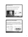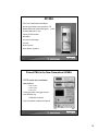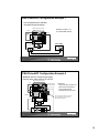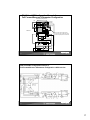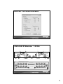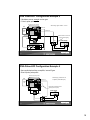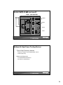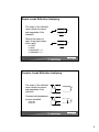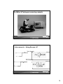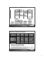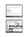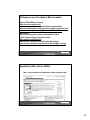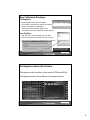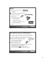
1
安捷倫科技高頻元件量測研討會 時間: 2006年 2月23日 地點: 高雄金典酒店 Packaging Development Trend of Integrated Analysis Sung-Mao Wu 安捷倫高頻元件量測研討會 Page 1 2/23/2006 Outline Development Trend for PKG -- PKG Technology Trend -- Why SiP and POP/PIP Challenges to PKG Integrity Design -- Design Challenges on Simulation, Measurement and Design -- Case I : Effective DK -- Case II : Impedance Control verify by TDR -- Case III: TDR FA Application -- Case IV : Substrate Ball Pad Design -- Case V : PDS Analysis Integrated Design -- Components of Optimization PKG Design -- Advanced PKG Analysis Flow -- Plan and Actions for PKG Design 安捷倫科技高頻元件量測研討會 2/23/2006 Page 2 1 Interesting Semiconductor World Fab/fabless Copper wafer Front/Back end solution Low K material Environment friendly 12” wafer Compact Size Low power consumption Naro meter tech Semiconductor Industry Integrated System Bio tech / New form chip IC/module/System Design Low cost High speed/high frequency Short Time to Market High thermal / Stress solution Worldwide strategy 安捷倫科技高頻元件量測研討會 2/23/2006 Page 3 Packaging Technology Trend Wire Bond Single Chip Package Wire Bond + FC Bond New Interconnection? Multiple Chip Package Stacked Package QFP BGA Stacked Die System in Package MCM PoP Flip Chip FC+WB PiP Chip Multi-Layer PCB 1995 Laminate 2 & 4 Layer Build-Up Substrate 2000 Functional Substrate (Active & Passive Chip) 2005 2010 安捷倫科技高頻元件量測研討會 2/23/2006 Page 4 2 Why SIP ? SoC IC Compare to Board Assembly: MicroPassives SIP Performance Enhancement component Thinner, Smaller, and Lighter Low Cost Compare to SOC Low Cost Memory IC Time to Market Board Assembly Sub-System Flexible Build-up Substrate Single Chip Solution Module SIP Platform Die Stacking Platform Flash SDRAM ASIC Package Stacking Platform Flash SDRAM Flash SDRAM ASIC ASIC 安捷倫科技高頻元件量測研討會 2/23/2006 Page 5 Die Stacking Package Trend • Smaller & Lighter Package Size 0.5mm • High Density Device in Package 0.8mm 1.0mm 1.2mm 1.4mm 2 die 3 die 4 die 5 die 7 die 安捷倫科技高頻元件量測研討會 2/23/2006 Page 6 3 PoP and PiP PoP Package/ Die Count Package Thickness Package Structure 2 PKG/ 3 Chip 2 PKG/ 3 Chip 2 PKG/ 4 Chip 3 PKG/ 7 Chip 1.6 mm Max 1.4 mm Max 1.2 mm Max 2.0 mm Max Flash Flash SDRAM ASIC W/B Type Flash F/C Type SDRAM ASIC Flash SDRAM ASIC SDRAM ASIC PiP 2 PKG/ 3 Chip 2 PKG/ 3 Chip 2 PKG/ 3 Chip 1.4 mm Max 1.2 mm Max 1.0 mm Max Package/ Die Count Package Thickness Package Structure Available 2006 2007 安捷倫科技高頻元件量測研討會 2/23/2006 Page 7 Fine Pitch Wire Bonding IC Feature Size (um) • Wire Bond pad Pitch (um) 0.25 0.18 0.13 0.09 0.065 50 45 40 35 80/40 70/35 60/30 50/25 40/20 90/45 80/40 70/35 60/30 50/25 100/50 90/45 80/40 70/35 60/30 60 (Single-In-Line) • Wire Bond Pad Pitch (um) (2 Row Staggered) • Wire Bond Pad Pitch (um) (Tri-Tier) •Wire Bond pad pitch (um ) ( Quad-Tier ) Leading-Edge Fine-Pitch Capabilities In-Line: 45 um; Staggered: 60 um; Tri-Tier: 70 um ; Quad-Tier: 80um Low k & Copper wafer capabilities available. 安捷倫科技高頻元件量測研討會 2/23/2006 Page 8 4 Trends of Packaging Technologies Focus Packages - Bumping, WLCSP, FCBGA, SIP, SCSP and modified LF package Small & Light Thin Thickness in Wafer, Substrate, Package Fine Pitch in Wire Bonding, Flip Chip Bond and Solder Ball High Density by Stacked Die, Package, MultiSubstrate Layer,Substrate Stacked, Staggered Via and Small Trace Via Hole Size - Good Thermal and Electrical Performance Green - High Speed and Low Thermal Resistance Cu / LowLow-K wafer, wafer Nano-technology - Green Solution Low Cost & Fast Time-to-market 12’’ 12’’ Wafer Capacity Total Turnkey Solution Matrix design, Multi-die, package Design LAB Design Support 安捷倫科技高頻元件量測研討會 2/23/2006 Page 9 Outline Development Trend for PKG -- PKG Technology Trend -- Why SiP and POP/PIP Challenges to PKG Integrity Design -- Design Challenges on Simulation, Measurement and Design -- Case I : Effective DK -- Case II : Impedance Control verify by TDR -- Case III: TDR FA Application -- Case IV : Substrate Ball Pad Design -- Case V : PDS Analysis Integrated Design -- Components of Optimization PKG Design -- Advanced PKG Analysis Flow -- Plan and Actions for PKG Design 安捷倫科技高頻元件量測研討會 2/23/2006 Page 10 5 Challenges to PKG Integrated Design Analysis Challenges ÆMulti-port parameters analysis and broadband calibration skill ÆDouble-side calibration and probing technology ÆSignal-integrity, SSN/SSO and IP drop ÆMixed-signal analysis ÆSubstrate On-line testing, like via, bump and ball…… Design Challenges to SiP ÆPKG selection for different thermal/electrical request ÆSubstrate Design integrated thermal/electrical solution. -- Embedded Die/passive, IPD, decoupling cap…… ÆPKG IP development. ÆDesign Guideline and constraint 安捷倫科技高頻元件量測研討會 2/23/2006 Page 11 Analysis Case I : Æeffective dielectric constant What is the effective Er of this mixture material ? Er = 3.2 Er = 6.0 安捷倫科技高頻元件量測研討會 2/23/2006 Page 12 6 Analysis Case I : ÆMeasurement and ADS setup VNA Long trace short trace Short trace Sample Probe station DUT: (Microstrip/Strip TL) same cross-section with different length 安捷倫科技高頻元件量測研討會 2/23/2006 Page 13 Analysis Case I : Æextraction result 4.5 m4 4.0 3.5 Effective dielectric constant 3.0 2.5 Er_preg Sim/mea comparison 200 m4 freq= 2.358GHz Er_preg=3.828 2.0 1.5 1.0 0.5 0.0 -0.5 -1.0 0 8.00 7.84 7.68 7.52 7.36 7.20 7.04 6.88 6.72 6.56 6.40 6.24 6.08 5.92 5.76 5.60 5.44 5.28 5.12 4.96 4.80 4.64 4.48 4.32 4.16 4.00 3.84 3.68 3.52 3.36 3.20 3.04 2.88 2.72 2.56 2.40 2.24 2.08 1.92 1.76 1.60 1.44 1.28 1.12 0.96 0.80 0.64 0.48 0.32 0.16 0.00 0.5 Mea -100 freq, GHz 0.4 loss_tan1 phase(S(6,5)) phase(S(2,1)) 100 Sim m5 freq=4.985GHz loss_tan1=0.011 0.3 Loss tangent 0.2 0.1 -200 m5 0 2 4 6 8 10 12 14 freq, GHz 16 18 20 22 24 26 0.0 0 1 2 3 4 5 6 7 8 9 10 freq, GHz Good Correlation between simulation and measurement Once we have the accurate the dielectric constant of mixture material of substrate, we can achieve good electrical substrate design. 安捷倫科技高頻元件量測研討會 2/23/2006 Page 14 7 Analysis Case II : ÆImpedance Control Verify by TDR/TDR System Signal Trace in 1st Layer W S T GND Plane in 2nd Layer T1 Dielectric Layer ε= 4.0 Design Condition: Substrate Type : 2 Layer Impedance Control : Differential Simulation Structure : Micro-Strip Line Trace Width (W): 0.39mm Trace Thickness (T): 22 um Dielectric Thickness (T1): 200um Separation (s): 0.15mm TDR Measurement Result 安捷倫科技高頻元件量測研討會 2/23/2006 Page 15 Impedance Control -- Manufacture Result and comparison SEM-single ended trace width measurement SEM-differential trace width/space measurement Design / Measurement Comparison Q2D Q2D TDR Trace width(um) 388.95(from drawing) 429um 429um Impedance comparison separation(um) Zodd(ohm) Zeven(ohm) Single ended(ohm) 41.2 58.8 50.9 150(from drawing) 38.1267 55.6689 47.5768/435um 116um 61.7 116um 42.4~42.8 52.3~53 安捷倫科技高頻元件量測研討會 2/23/2006 Page 16 8 Analysis Case III ÆFA Application ▼ TDR of bare, good, and failure sample bare substrate Open waveform good unit 1 2202 T4 failure Slight difference on the chip capacitance charge curve – A possible reason of this phenomenon is the IMC makes the interface resistance between wire and bond pad growing, which causes the charge current different. good unit 2 IMC Chip capacitance 安捷倫科技高頻元件量測研討會 2/23/2006 Page 17 Analysis Case IV : ÆBall pad effect analysis Void the plane above ball pad area at PWR/GND will reduce the capacitance, Ball_Pad1 No Void Ball_Pad2 Void layer3 Ball_Pad3 dB(Ball_Pad3_UP_1112..S(2,1 dB(Ball_Pad2_UP_1112..S(2,1 dB(Ball_Pad1_UP_1112..S(2,1 Void PWR/GNG plane above the ball land on Layer3 Measurement Result 0 -5 -10 -15 -20 -25 0 Void layer2&3 2 4 6 8 10 12 14 16 18 20 freq, GHz 安捷倫科技高頻元件量測研討會 2/23/2006 Page 18 9 Analysis Case V : PDS Analysis -- Measurement setup 27mm 27mm Top view Bottom view 安捷倫科技高頻元件量測研討會 2/23/2006 Page 19 Analysis Case V : Æ Measurement and Simulation Result (Test Board only) Port 1 Port 2 S21_dB Field propagation @750MHz 安捷倫科技高頻元件量測研討會 2/23/2006 Page 20 10 Analysis Case V : Æcomparison with bare PCB, Package and BGA+PCB Bare PCB Noise coupling between PKG&PCb? package only BGA and PCB Effect of package -5 -10 -15 S21 (dB) -20 -25 -30 -35 -40 -45 -50 -55 0 0.5 1 1.5 2 2.5 3 3.5 4 4.5 5 Frequency (GHz) 安捷倫科技高頻元件量測研討會 2/23/2006 Page 21 Outline Development Trend for PKG -- PKG Technology Trend -- Why SiP and POP/PIP Challenges to PKG Integrity Design -- Design Challenges on Simulation, Measurement and Design -- Case I : Effective DK -- Case II : Impedance Control verify by TDR -- Case III: TDR FA Application -- Case IV : Substrate Ball Pad Design -- Case V : PDS Analysis Integrated Design -- Components of Optimization PKG Design -- Advanced PKG Analysis Flow -- Plan and Actions for PKG Design 安捷倫科技高頻元件量測研討會 2/23/2006 Page 22 11 Components of Optimization Package Design Characterization Lab capability on Electrical, Thermal, Stress and Material Substrate: laminate, build-up, ceramic, RLC embed Design Rule/Spec for substrate layout •Knowing Electrical Characteristics deep inside •Provide package solutions from advanced pkg technology Wire & Bumping Pkg options: structure, cost, thermal, board level... Leadframe: L/F for SOP/QFP etc, L/F for BCC/QFN etc. 安捷倫科技高頻元件量測研討會 2/23/2006 Page 23 Integrity Design Flow for Advanced PKG Substrate Design / Pre-simulation Software •Design Guideline and Constraint Transfer interface Simulation Quasi-State EM Simulator •Whole PKG modeling extracting High Frequency/Speed Simulator •3D Field solver •FTDT simulator •2.5D Momentum •PDS Simulator POST-Analysis Capability & Integrated plane •Broadband modeling •Signal Integrity (SI) •PDS analysis •EMI/EMC analysis •data flow control plane •PKG IP Development System Integrity Analysis and Design Guide for Advance Package Hardware Frequency Domain •VNA/PNA with PLTS/ADS 8722ES (40GHz, 2-port) 8364B (50GHz, 4-port) •Impedance Analyzer •Spectrum analyzer Measurement Plane •Probe Station Single-side 2-port Double-Side Multi-port •High Performance Probe (50GHz) •High Performance cable (50GHZ) Time Domain •Time Domain Reflectometer with TDA/ •High Speed Pattern Generator Design Constraint & PKG IP 安捷倫科技高頻元件量測研討會 2/23/2006 Page 24 12 Plan and Actions for PKG Design Substrate Design Integrity Electrical Performance -Design Integrity Electrical performance flow -Design Rule and Constraint setting for SiP PKG Application, like RF Module, optical and wireless PKG Active/Passive Device analysis capability -Embedded passive (RF-MEMS, Substrate embedded RLC) analysis and IP-development -Sub-system measurement capability setting for advanced PKG Co-Design and Co-development with key partners -Co-working with key partners for more close and detail study in Wireless, Optical or RF module 安捷倫科技高頻元件量測研討會 2/23/2006 Page 25 Contacts z Samuel_Wu, Leader of Electrical Lab E-mail: [email protected] Phone: 886-7-3617131 ext. 15290/85290 Fax: 886-7-3613094 z Mark_Li, Project Engineer of Electrical Lab E-mail: [email protected] Phone: 886-7-3617131 ext. 15291/85291 Fax: 886-7-3613094 ASE, Inc (Kaohsiung) 26, Chin 3rd Rd., 811, Nantze Export Processing Zone Kaohsiung, TAIWAN Website: www.aseglobal.com 安捷倫科技高頻元件量測研討會 2/23/2006 Page 26 13 THE END Thank You For Your Listening 安捷倫科技高頻元件量測研討會 2/23/2006 Page 27 14 PNA Based Solutions - Pulsed RF S-Parameter Measurements - Multiport Test Solutions - Physical Layer Test Systems Agilent Technologies Ltd. Ming-Fan, Tsai Project Manager Feb, 23, 2006 安捷倫科技高頻元件量測研討會 Page 1 Feb.23, 2006 Pulsed-RF S-Parameter Applications Using The Agilent PNA Series Network Analyzer 安捷倫科技高頻元件量測研討會 Page 2 Feb.23, 2006 1 Agenda • Why Measure in Pulsed Mode and the DUTs We Test – Wafer Test – Power Amplifiers – Antenna RCS – T/R Modules • Review of Pulsed Measurements • Wideband synchronous • Narrowband asynchronous • Evolution of Pulsed VNAs from Agilent • 8510, 85108, 85120, CTS Platform to PNA • Test Sets Available 安捷倫科技高頻元件量測研討會 Feb.23, 2006 Page 3 Why Test Under Pulsed Conditions? • Device may behave differently between CW and pulsed stimuli • Bias changes during pulse might affect RF performance • Overshoot, ringing, droop may result from pulsed stimulus • Measuring behavior within pulse is often critical to characterizing system operation (radars for example) • CW test signals would destroy DUT • High-power amplifiers not designed for continuous operation • On-wafer devices often lack adequate heat sinking • Pulsed test-power levels can be same as actual operation 安捷倫科技高頻元件量測研討會 Page 4 Feb.23, 2006 2 On-Wafer Amplifier Test and Modeling •Most applications are at microwave frequencies •Devices lack adequate heatsinking for CW testing, so pulsed-RF used as a test technique to extract S-parameters •Arbitrary, stable temperature (isothermal state) set by adjusting duty cycle •Duty cycles are typically < 1% •Often requires synchronization of pulsed bias and pulsed RF stimulus 安捷倫科技高頻元件量測研討會 Feb.23, 2006 Page 5 Wireless Communications Systems • TDMA-based systems often use burst mode transmission • Saves battery power • Minimizes probability of intercept • Power amplifiers often tested with pulsed bias • Most of wireless communications applications ≤ 6 GHz 安捷倫科技高頻元件量測研討會 Page 6 Feb.23, 2006 3 Pulsed Antenna Test • About 30% of antenna test involves pulsed-RF stimulus • Test individual antennas, complete systems, or RCS • RCS (Radar Cross Section) measurements often require gating to avoid overloading receiver 安捷倫科技高頻元件量測研討會 Feb.23, 2006 Page 7 Component-Level Characterization • Accurate characterization of components such as amplifiers, mixers, filters, and antennas is critical for effective system simulation • Pulsed-RF stimulus crucial for many components in A/D applications such as AESA Phased arrays and the individual T/R Modules that are used in such systems Transmit / Receive Module Receive Module 安捷倫科技高頻元件量測研討會 Page 8 Feb.23, 2006 4 Radar and Electronic-Warfare •Biggest market for pulsed-RF testing •Traditional applications ≤ 20 GHz •Many now include Multi-Mode Ka-Band •Devices include • amplifiers • T/R modules AN/APG-79 F16C Block 60 • up/down converters Pave-Paws AN/APG-81 JSF 安捷倫科技高頻元件量測研討會 Feb.23, 2006 Page 9 Agenda • Why Measure in Pulsed Mode and the DUTs We Test – Wafer Test – Power Amplifiers – Antenna RCS – T/R Modules • Review of Pulsed Measurements • Wideband synchronous • Narrowband asynchronous • Evolution of Pulsed VNAs from Agilent • 8510, 85108, 85120, CTS Platform to PNA • Test Sets Available 安捷倫科技高頻元件量測研討會 Page 10 Feb.23, 2006 5 VNA Pulsed-RF Measurements VNA data display Magnitude and phase data averaged over duration of pulse data point Frequency domain Average Pulse Swept carrier Data acquired only during specified gate width and position within pulse Frequency domain Point-in-Pulse CW Data acquired at uniformly spaced time positions across pulse (requires a repetitive pulse stream) Pulse Profile dB Magnitude Time domain deg Phase Note: there may not be a one-to-one correlation between data points and the actual number of pulses that occur during the measurement 安捷倫科技高頻元件量測研討會 Feb.23, 2006 Page 11 Pulsed-RF Data Acquisition (Time Domain View) Freq 6 carrier freq Pulsed-RF ... Freq 5 Point-in-Pulse Freq 4 Freq 3 Freq 2 Freq 1 Trace point 1 Trace point 2 Trace point 3 Trace point 4 gate delay Trace point 5 Delay 6 ... Gate Delay 4 Delay 3 Note: the number of pulses per data point varies with PRF and IF bandwidth Delay 2 Delay 1 Page 12 t ... Delay 5 Pulse Profile Trace point 1 Trace point 6 Trace point 2 Trace point 3 Trace point 4 Trace point 5 Trace point 6 t ... 安捷倫科技高頻元件量測研討會 Feb.23, 2006 6 Pulse-to-Pulse (Single Shot) Measurements • Carrier remains fixed in frequency • Measurement point in pulse remains fixed with respect to pulse trigger (requires wideband detection technique) • One data point for each successive pulse, no pulses skipped • Display magnitude and/or phase versus time One data point for each successive pulse, no pulses skipped CW pulses P1 P2 VNA data display P3 P4 P5 P6 … Time domain 安捷倫科技高頻元件量測研討會 Feb.23, 2006 Page 13 Pulsed S-parameter Measurement Modes Wideband/synchronous acquisition • Majority of pulse energy is contained within receiver bandwidth • Incoming pulses and analyzer sampling are synchronous (requires a pulse trigger, either internal (8510) or external (PNA) • Pulse is “on” for duration of data acquisition • No loss in dynamic range for small duty cycles (long PRI's), but there is a lower limit to pulse width Receiver BW Pulse trigger Time domain Frequency domain 安捷倫科技高頻元件量測研討會 Page 14 Feb.23, 2006 7 Typical Hardware Setup For Wideband Detection Point-in-Pulse and Pulse-to-Pulse External pulse generator (e.g., 81110A/81111A) Output 1 PNA (20, 40, 50, or 67 GHz) with: • 014 Configurable test set • UNL Source attenuators • 080 Frequency offset mode To TRIG IN (rear panel) 10 MHz Ref Output 2 Cplr Thru Src Out Ref In Z5623A H81 2-20 GHz RF modulator DUT Note: pulse generator controls timing Additional PNA setup: • step sweep • frequency offset on (0 Hz) • Auto IF gain = off 安捷倫科技高頻元件量測研討會 Feb.23, 2006 Page 15 Alternate Hardware Setup For Wideband Detection PNA (20, 40, 50, or 67 GHz) with: • 014 Configurable test set • UNL Source attenuators • 080 Frequency offset mode External pulse generator (e.g., 81110A/81111A) TRIG OUT (rear panel) to pulse gen EXT INPUT Output 1 10 MHz Ref Output 2 Src Out Cplr Thru Ref In Z5623A H81 2-20 GHz RF modulator DUT Note: PNA controls timing Additional PNA setup: • step sweep • frequency offset on (0 Hz) • Auto IF gain = off 安捷倫科技高頻元件量測研討會 Page 16 Feb.23, 2006 8 Minimum Pulse Widths for Point-in-Pulse Measurements Using Wideband Detection Maximum IF bandwidth Minimum pulse width IF auto-gain mode* PNA models (20, 40, 50, 67 GHz) 40 kHz 50 us Yes PNA-L models (2-port, 20, 40, 50 GHz) 250 kHz 10 us Yes PNA-L models (2-port, 6, 13.5 GHz; 4-port, 20 GHz) 600 kHz 2 us No * Note: for point-in-pulse measurements, the IF auto-gain mode should be turned off (i.e., set IF gains manually) 安捷倫科技高頻元件量測研討會 Feb.23, 2006 Page 17 Fastest PRI/PRF for Pulse-Pulse Measurements Using Wideband Detection Conditions: point sweep; external trigger, CW sweep; IF autogain=off Maximum IF bandwidth Minimum PRI Maximum PRF PNA models (20, 40, 50, 67 GHz) 40 kHz 170 us 5.9 kHz PNA-L models (2-port, 20, 40, 50 GHz) 250 kHz 80 us 12.5 kHz PNA-L models (2-port, 6, 13.5 GHz; 4-port, 20 GHz) 600 kHz 40 us 25 kHz PRI CW pulses P1 P2 P3 P4 P5 P6 … 安捷倫科技高頻元件量測研討會 Page 18 Feb.23, 2006 9 Pulsed S-parameter Measurement Modes Narrowband/asynchronous acquisition • Extract central spectral component only; measurement appears CW • Data acquisition is not synchronized with incoming pulses (pulse trigger not required) • Sometimes called “high PRF” since normally, PRF >> IF bandwidth • “Spectral nulling" technique achieves wider bandwidths and faster measurements • No lower limit to pulse width, but dynamic range is function of duty cycle IF filter Time domain IF filter D/R degradation = 20*log[duty cycle] Frequency domain 安捷倫科技高頻元件量測研討會 Feb.23, 2006 Page 19 Filtered Output Using Spectral Nulling 1 1 0.9 0.9 0.8 0.8 0.7 0.7 X 0.6 0.5 0.6 0.5 0.4 0.4 0.3 0.3 0.2 0.2 0.1 0.1 0 -3 -2 -1 0 1 2 3 0 -3 4 x 10 Pulsed spectrum Digital filter (with nulls aligned with PRF) -2 -1 0 Output 1 2 3 4 x 10 • With “custom” filters, number of filter sections (M) can be chosen to align filter nulls with pulsed spectral components • With spectral nulling, reject unwanted spectral components with much higher IF bandwidths compared to using standard IF filters • Result: faster measurement speeds! 安捷倫科技高頻元件量測研討會 Page 20 Feb.23, 2006 10 Typical Hardware Setup (Narrowband) External pulse generator (e.g., 81110A/81111A) GPIB Output 1 PNA (20, 40, 50, or 67 GHz) with: • 014 Configurable test set • UNL Source attenuators • 080 Frequency offset mode • 081 Reference switch • H11 IF access • H08 Pulsed-RF measurement capability • 016 Receiver attenuators (optional) Pulse 2 drive to PULSE IN B (for point-inpulse measurements) 10 MHz Ref Output 2 PNA Src Out Cplr Thru Ref In Z5623A H81 2-20 GHz RF modulator DUT Option H08 VB application/DLL 安捷倫科技高頻元件量測研討會 Feb.23, 2006 Page 21 Agenda • Why Measure in Pulsed Mode and the DUTs We Test – Wafer Test – Power Amplifiers – Antenna RCS – T/R Modules • Review of Pulsed Measurements • Wideband synchronous • Narrowband asynchronous • Evolution of Pulsed VNAs from Agilent • 8510, 85108, 85120, CTS Platform to PNA • Test Sets Available 安捷倫科技高頻元件量測研討會 Page 22 Feb.23, 2006 11 85108A First True pulsed Network Analyser Still the most widely used system for TR Module R&D and manufacturing test (>100 off world-wide still in use) Wholly COTS solution Affordable Low cost of ownership Low risk Point-on-pulse Pulse profile, repetitive 安捷倫科技高頻元件量測研討會 Feb.23, 2006 Page 23 Pulsed PNA is the New Generation 85108A COTS stand alone hardware can perform: – Point-on-pulse – Pulse-to-Pulse – Pulse profile Timing generator can trigger custom user hardware e.g. TR Module controller Very much faster measurement speed 安捷倫科技高頻元件量測研討會 Page 24 Feb.23, 2006 12 Comparing the 8510 and PNA 8510 (85108A) • Dominant mode is wideband detection • Detection is done BEFORE analog-to-digital conversion • Analog synchronous detector produces baseband I/Q output (detector bandwidth = 1.5 MHz) • Pulse profiling achieved by varying sample point of baseband pulses • Trade off speed and dynamic range with averaging PNA • Dominant mode is narrowband detection • All processing (filtering and detection) is done digitally • Widest bandwidth = 35 kHz • Pulse profiling achieved with analog switches that gate IF (or RF) signals • Trade off speed and dynamic range with variable IF bandwidths and averaging PNA-L • Dominant mode is wideband detection • All processing (filtering and detection) is done digitally • Widest bandwidth = 600 kHz • Trade off speed and dynamic range with variable IF bandwidths and averaging 安捷倫科技高頻元件量測研討會 Feb.23, 2006 Page 25 Agilent TR Module Test Systems 85120A S10 Family 84000A Family 安捷倫科技高頻元件量測研討會 Page 26 Feb.23, 2006 13 Agilent TR Module Test Systems continued CTS-I Family CTS-II Family 安捷倫科技高頻元件量測研討會 Feb.23, 2006 Page 27 Pulse Summary Wideband/Synchronous Narrowband/Asynchronous Advantages Disadvantages Constant dynamic range Lower pulse width limit Elevated noise floor 8510 PW > 1 us PNA PW > 50 us/10 us/2 us** PNA Options None required Average Point-in-pulse Measurements Pulse profile Pulse-to-pulse Narrow pulse widths Dynamic range loss with small duty cycles No pulse-to-pulse Limited* (High PRF Mode) PW > 20 ns (limited by IF gate) H11/H08*** Average Point-in-pulse Pulse profile * No nulling, no point-in-pulse ** PNA/PNA-L 2-port 20, 40, 50 GHz/PNA-L 2-port 6, 13.5, 4-port 20 GHz *** Option H08 is usually used in conjunction with Option H11. Without H11, the user can perform average pulse, or point-in-pulse measurements using external RF gates. 安捷倫科技高頻元件量測研討會 Page 28 Feb.23, 2006 14 Agenda • Why Measure in Pulsed Mode and the DUTs We Test – Wafer Test – Power Amplifiers – Antenna RCS – T/R Modules • Review of Pulsed Measurements • Wideband synchronous • Narrowband asynchronous • Evolution of Pulsed VNAs from Agilent • 8510, 85108, 85120, CTS Platform to PNA • Test Sets Available 安捷倫科技高頻元件量測研討會 Feb.23, 2006 Page 29 Z5623A Hxx RF Modulators • Z5623A H81 (2-20 GHz) • Expected to be most common configuration ($43K) • Contains pin switch, amplifier, directional coupler • Use jumpers to bypass internal amp or use high-power external amp • Other quoted test sets: • Z5623A H83 1-20 GHz Bidirectional (two pin switches) $80K • Z5623A H84 20-40 GHz Bidirectional (two pin switches) $105K • Z5623A H85 20-40 GHz Unidirectional, no amplifier $35K • Z5623A H86 2-40 GHz Unidirectional, dual band (incl. band switch) $65K • Customization via Agilent’s “Special Handling” group: • Different frequency ranges • No amplifier or higher power amplifiers • High power components Z5623A H81 安捷倫科技高頻元件量測研討會 Page 30 Feb.23, 2006 15 PNA Pulsed-RF Configuration Example 1 • User-supplied external modulator • Average pulse measurements 81110A family pulse generator Advantage: simplest – use any standard PNA with 014 GPIB Pulse out 10MHz Ref Src Out Power Supply Cplr Thru RF in Com +25 -25 RF out TTL DC(+) DC(-) 安捷倫科技高頻元件量測研討會 Feb.23, 2006 Page 31 PNA Pulsed-RF Configuration Example 2 • Modulator test set, internal receiver gates • Point-in-pulse, pulse profile of S21 and S11 81110A family pulse generators GPIB One output channel drives RF modulator Trigger Advantages: • easily make point-in-pulse and pulse profile measurements • more sophisticated RF modulator boosts port power 10 MHz Ref Src Out PNA Three output channels drive internal receiver gates A, B, and R1 for point-in-pulse and pulse-profile measurements Ref In DUT Z5623A H81 pulsed-RF test set 安捷倫科技高頻元件量測研討會 Page 32 Feb.23, 2006 16 PNA Pulsed-RF Configuration Example 3: Full Forward/Reverse S-Parameter Configuration 81110A family pulse generators GPIB One output channel drives RF modulator Trigger 10 MHz Ref Three output channels drive internal receiver gates A, B, and R1/R2 for pointin-pulse and pulse-profile measurements PNA DUT 安捷倫科技高頻元件量測研討會 Page 33 Feb.23, 2006 PNA Pulsed-RF Configuration Example 3: Full Forward/Reverse S-Parameter Configuration a different view 安捷倫科技高頻元件量測研討會 Page 34 Feb.23, 2006 17 Z5623A H83 – H84 Test Set Control Macro 安捷倫科技高頻元件量測研討會 Feb.23, 2006 Page 35 Z5623A H83 RF Modulator 1-20 GHz AMP 1 TERM 1 2 1 3 4 SW2 4 1 AMP 2 TERM AMP 1 TERM AMP 2 TERM 2 2 3 3 1 2 4 SW5 4 3 SW6 SW3 1 2 2 SW1 4 16 dB SW 7 Source Filter IN IN Pulse Out 6$ 1 SW4 3 CPLR1 AMP OUT Pulse 1 IN AMP IN Source CPLR OUT IN CPLR THRU 60 dB ATN2 ATN1 10/20/30 10/20/30 RCVR R1 IN 3 60 dB 4 16 dB SW8 CPLR2 RCVR R2 IN CPLR THRU CPLR Source AMP OUT IN IN AMP OUT Pulse 2 IN Pulse Out Filter Source IN IN Z5623AH83 PULSE TEST SET, 1 GHz to 20 GHz RCVR R1 OUT AMP IN SOURCE OUT FILTER IN FILTER IN PORT STATUS "GPIB ONLY" SOURCE OUT AMP IN RCVR R2 OUT SOURCE IN SOURCE IN CPLR THRU AMP OUT CPLR IN AVOID STATIC DISCHARGE PULSE OUT PULSE OUT PULSE 1 IN CPLR IN AMP OUT CPLR THRU PULSE 2 IN LINE 00 TTL 0,5 VDC, 10K OHM 1 CAUTION: SEE MANUAL FOR MAXiMUM POWER RATINGS CAUTION: SEE MANUAL FOR MAXiMUM POWER RATINGS 安捷倫科技高頻元件量測研討會 Page 36 Feb.23, 2006 18 PNA Pulsed-RF Configuration Example 4 • Modulator test set, external receiver gate • Point-in-pulse, pulse profile 81110A family pulse generator GPIB Advantage: gate widths < 20 ns Pulse1 out 10 MHz Ref Pulse2 out Src Out External switch in receiver B loop for external gating Ref In TTL Power Supply Com +25 -25 DC(+) DC(-) Z5623A H81 pulsed-RF test set 安捷倫科技高頻元件量測研討會 Feb.23, 2006 Page 37 PNA Pulsed-RF Configuration Example 5 • User-supplied pulsed bias to amplifier, internal IF gate • Point-in-pulse, pulse profile 81110A family pulse generator GPIB Pulse1 out Advantage: pulsed bias to amplifier (with CW input) 10 MHz Ref Pulse2 drive to internal receiver gates (for point-in-pulse) Power Supply CW Pulsed-RF Com +25 -25 安捷倫科技高頻元件量測研討會 Page 38 Feb.23, 2006 19 PNA Pulsed-RF Configuration Example 6 • Customer-supplied pulsed bias and pulsed RF, internal IF gate • Point-in-pulse, pulse profile 81110A family pulse generators GPIB Trigger Pulse1 out Advantage: both pulsed bias and pulsed-RF stimulus 10 MHz Ref Src Out Pulse3 drive to internal receiver gate B (for point-inpulse) Cplr Thru RF in Power Supply RF out Pulse2 out TTL DC(-) Com +25 -25 DC(+) 安捷倫科技高頻元件量測研討會 Feb.23, 2006 Page 39 Summary • Testing with pulsed-RF is very important for radar, EW, and wireless comms systems • Narrowband detection: • Spectral nulling technique improves measurement speed • For radar and wireless comms applications, offers superior dynamic range/speed • No lower limit to pulse widths 0 -10 -20 -30 S21 (dB) • Although the PNA uses different hardware and detection techniques than the 8510, measurement results are essentially the same! -40 PNA -50 8510 -60 -70 • PNA also offers numerous platform benefits: -80 -90 12.74 12.49 12.24 11.99 9.99 11.74 11.49 9.74 11.24 10.99 9.49 9.24 10.74 10.49 8.99 8.74 10.24 8.49 8.24 7.99 7.74 -100 Frequency (GHz ) • Measurement flexibility (32 channels, 64 traces, 16 windows, 16,001 points) • Connectivity (LAN, USB, …) • Automation (open Windows®, COM, SCPI …) • Ease of use (built-in HELP, Cal Wizard, ECal …) 安捷倫科技高頻元件量測研討會 Page 40 Feb.23, 2006 20 Resources • www.agilent.com/find/pulsedrf 安捷倫科技高頻元件量測研討會 Page 41 Feb.23, 2006 Multiport - PNA based solutions 安捷倫科技高頻元件量測研討會 Page 42 Feb.23, 2006 21 Agenda • Target Applications • PNA Multiport Test Solutions • Specials vs. Standard product • Customer data required for new multiport specials • Further Information 安捷倫科技高頻元件量測研討會 Feb.23, 2006 Page 43 Target Applications • Front End Module (FEM) • Cellular FEM (see next slide) • WLAN FEM (Base Band not included, 2.4G & 5G dual band) • Filter array (see next slide) – Multiple filter in single package – Duplexer/Coupler array (see next slide) – Multiple Duplexer/Coupler in single package • High Frequency Multiport devices – Triplexer, power splitter, multiport coupler etc. – RF module, RF switch IC • High power device testing 安捷倫科技高頻元件量測研討會 Page 44 Feb.23, 2006 22 Cellular FEM #1 (Dual band, 1xEV,GPS) Diversity Rx 安捷倫科技高頻元件量測研討會 Page 45 Feb.23, 2006 Cellular FEM #2 (Quad band, UMTS,GSM) 安捷倫科技高頻元件量測研討會 Page 46 Feb.23, 2006 23 WLAN FEM(2.4G・5G dual band) 2.4 GHz / 5 GHz WLAN FEM BPF 2.4 GHz Rx 5 GHz Rx LNA 2.4 GHz Tx Diversity SW 5 GHz Tx Diplexer PA 安捷倫科技高頻元件量測研討會 Feb.23, 2006 Page 47 Multiport & High Power Testing Devices • Typical High Frequency devices – Switches, Couplers, Power Splitter/Divider and etc.. – Filter/Coupler array • Multiport and high power – PA Cellular/WLAN FEM with PA – RF switch IC ( Switch filters) 安捷倫科技高頻元件量測研討會 Page 48 Feb.23, 2006 24 Key Measurement Requirements Cellular FEM without PA • IL, RL for each path up 12.75GHz • Isolation – Frequency > 3x Carrier – Signal level 0dBm or –10dBm • Switch distortion – Frequency up to 12.75GHz in R&D – Signal Level up +36dBm UMTS850 UMTS1900 GSM Tx 安捷倫科技高頻元件量測研討會 Feb.23, 2006 Page 49 Key Measurement Requirements BPF WLAN FEM with PA – – – – Gain, 1dB Compression, Pout,PAE RL Isolation Harmonics distortion • Frequency Cellular > 3x Carrier Frequency • Frequency(WLAN): 17.4GHz • Power : 25dBm(WLAN) 36dBm(GSM/Mobile) 2.4 GHz Rx 5 GHz Rx LNA 2.4 GHz Tx Diversity SW 5 GHz Tx Diplexer PA 安捷倫科技高頻元件量測研討會 Page 50 Feb.23, 2006 25 Agenda • Target Applications • PNA Multiport Test Solutions • Specials vs. Standard product • Customer data required for new multiport specials • Further Information 安捷倫科技高頻元件量測研討會 Feb.23, 2006 Page 51 New PNA Rev 6.0 Firmware (Available December 2005) Sets GP-IB address, or Test Set IO address Select Testset Control File base on test set New Functionality: • External test set control • “Any 2-port” capability Set physical ports in ANY order Set control lines (if test set has them) on a per channel basis 安捷倫科技高頻元件量測研討會 Page 52 Feb.23, 2006 26 PNA/PNA-L Option 550 Measure SParameter Balanced Receivers Applications • New firmware option 550 for the PNA/PNA-L adds full 4port capability and differential measurements to a two port network analyzer • CPL Dec 1, 2005 • $7k RFP 安捷倫科技高頻元件量測研討會 Feb.23, 2006 Page 53 Variety Summary Switching Extension Hybrid Special Multiport Test Varieties SCMM Signal Conditioning 安捷倫科技高頻元件量測研討會 Page 54 Feb.23, 2006 27 Test Sets Overview Platform Description Benefits 87050A-Hxx/Kxx Switching test sets. Lower cost No coupler inside test set N4419/20/21B/H67 Extension test sets 4-port differential to 67Ghz Coupler on each port Z5623A-Hxx/Kxx Depend on the particular option Meets customer specific req’ts Mixing of Switching and Extension test sets 安捷倫科技高頻元件量測研討會 Feb.23, 2006 Page 55 Agilent’s Promoted Multiport Products & Specials 安捷倫科技高頻元件量測研討會 Page 56 Feb.23, 2006 28 Agilent PNA > 4-port Products offering Freq. Coverage: PNA Based Unit & Ext. Test set Total Test Ports 300 KHz – 20 GHz N5230A opt. 245 & Z5623AK64 6 300 KHz – 20 GHz N5230A opt. 245 & Z5623AK66 14 300 KHz – 20 GHz N5230A opt. 245 & Z5623AKxx 20 .010 – 40GHz E8363/4B or E8361A & 87050A-K62* 6 * 2-port cal only 安捷倫科技高頻元件量測研討會 Page 57 Feb.23, 2006 Multiport Specials – Variety • Extension Test Sets – Extension test sets provide signal paths from the network analyzer access ports to the test set. All test ports to the DUT are Coupler or Bridge base. Provides greater sensitivity. 安捷倫科技高頻元件量測研討會 Page 58 Feb.23, 2006 29 Multiport Specials – Variety • Hybrid Test Sets – Hybrid test sets are a combination of the switching and extension types. Test ports can be either switched or coupler bridge based. 安捷倫科技高頻元件量測研討會 Feb.23, 2006 Page 59 Multiport Specials – Variety • Switching Test Sets GPIB J1 – Switching test sets provide signal paths from the network analyzer test ports to the DUT. A3 Driver Daughter Board A2 Controller Interface Mother Board A1 Power Supply J74-J79 J50-J55 A4 LCD Controller Board C J53 2 20058 20062 C S50 C S52 1 1 J54 20061 J52 J50 Z5623-60013 2 20060 C 20059 20051 S54 2 1 J51 S53 1 J55 C 2 C 2 1 S51 20054 20055 20056 S55 2 20052 C2 C1 1 20053 C3 20057 C C4 C6 C5 Z5623-60012 1 2 34 5 67 8 9 Open / Collector Lines Reflection R1 R2 R3 A T1 T2/3 Transmission GPIB J1 (Type-N) Z5623A Option H46 A3 Driver Daughter Board A2 Controller Interface Mother Board A1 Power Supply J14 J15 J10-J15 87050-60055 Sw15 Sw14 w3 2 w4 3 w23 w2 Sw12 2 3 5 6 w14 Sw11 2 3 w15 5 6 Sw10 2 3 5 w10 w17 w9 w19 w16 1 2 1 2 1 w11 2 1 3 5 6 w13 w12 2 1 2 1 2 6 w18 w8 w7 w6 3 J10 J13 Sw13 J11 w5 2 J12 w22 J74-J79 J10-J15,J50-J57 A4 LCD Controller Board w20 2 1 2 1 2 w21 J50-J57 87050-60053 Sw50 C w1 Sw51 C w1 Sw52 C w1 Sw53 C w1 Sw54 C w1 Sw55 C w1 Sw56 C w1 Sw57 C w1 Z5623-60013 1 2 3 4 5 6 7 8 9 Open / Collector Lines Port 8 Port 7 Port 6 Port 5 Port 4 Port 3 Port 2 Port 1 Reflection (Type-N) Transmission (Type-N) (Type-N) Z5623A Option H48 安捷倫科技高頻元件量測研討會 Page 60 Feb.23, 2006 30 Multiport Specials – Variety • SCMM – Single connection multiple measurement test sets allow the user to make different types of measurements with out having to disconnect there DUT form the test set. Driver Daughter Board Controller Interface Mother Board Power Supply Display LCD Board SW 12 5 SW 10 2 6 5 2 3 4 6 SW 14 SW 15 5 3 6 4 1 1 3 SW 11 1 1 5 2 21 2 1 6 4 1 3 2 21 5 2 1 6 4 21 1 6 4 3 5 2 2 1 21 6 2 1 4 21 Aux1 3 SW 13 1 3 2 6 5 2 3 2 SW 61 SW 50 A i/p 1-4 5 SW 17 SW 16 2 1 21 2 1 2 3 4 5 10 9 6 7 8 Test Ports 11 Aux2 12 B i/p 4-1 Agilent 8720D Option K22 Multi-Function Switch Matrix 安捷倫科技高頻元件量測研討會 Feb.23, 2006 Page 61 Multiport Specials – Variety • Signal Conditioning – Test sets that require couplers, attenuators, amplifiers, filters and mixers that may or may not directly connect to the DUT. A Normal Mode P1 R1 Z5623A Opt H61 IF DUT MIXER isolator LO D UT PORT LO RF OU T Up/Down Filter/Mixer IN Source OUT PNA Coupler IN R2 Source IN PNA P2 Coupler OUT RF IF B OUT M1 B LO B IN B IN IN LO EXTOUT B OUT Filter/Mixer OU T IN LO IN PORT Source 安捷倫科技高頻元件量測研討會 Page 62 Feb.23, 2006 31 Agenda • Target Applications • PNA Multiport Test Solutions • Specials vs. Standard product • Customer data required for new multiport specials • Further Information 安捷倫科技高頻元件量測研討會 Feb.23, 2006 Page 63 Multiport Specials – Why Specials? • Offer solutions for applications which can not be addressed with existing or standard products • Increase sales of CTD standard products • Leverage standard platforms & OF capabilities to develop product extensions • • Fastest development-shipment time for new opportunities & competitive battles Helps to identify market needs and trends of specific applications 安捷倫科技高頻元件量測研討會 Page 64 Feb.23, 2006 32 Multiport Specials –Specials vs. Standard product Multiport Special – Custom – Does not follow the NPI PLC process – Fast development to shipment – Typical supplemental performance – Provide just enough performance • Functional Certificate • Return to Factory support Standard Product – Follows the NPI PLC process – Specifications with uncertainties. – Box and System level performance • Calibration Certificate • Return to Bench support • Verification test 安捷倫科技高頻元件量測研討會 Feb.23, 2006 Page 65 Multiport Specials –Test Set vs. System Performance Multiport Test Set • Typical supplemental performance specifications of the test set. • Measures the Insertion Loss, Port Match, and path Isolation between ports. • Provide just enough performance • Functional Certificate System Level (PNA and Test Set) • Raw or Corrected system performance is not provided. • Customers must take into consideration the performance of the PNA, Test Set, cabling, fixtures, and other peripherals to characterize their system level performance. • Once established that system level performance meets the application requirements. The customer can now define the PNA Multiport Test Solution and calibrate the system. • The customer can define a system verification method by using either a golden standard or by establishing an additional type of verification process. 安捷倫科技高頻元件量測研討會 Page 66 Feb.23, 2006 33 Agenda • Target Applications • PNA Multiport Test Solutions • Specials vs. Standard product • Customer data required for new multiport specials • Further Information 安捷倫科技高頻元件量測研討會 Feb.23, 2006 Page 67 Multiport Qualification Form • Most >4-port applications unique • Define customer needs upfront • Reduces time to quote and minimizes error FE/AE fill out with customer and email back to CTD/Say Phommakesone Qualification Form for Multiport Device Device Description and Specifications Describe the device and application (please attach block diagram of device) _______________________________________________________________________________ _______________________________________________________________________________ _______________________________________________________________________________ _______________________________________________________________________________ _______________________________________________________________________________ _____________________________________ Number of device ports: ______ Port impedance: ___ 50 ohms ___ 75 ohms Connector type(s):__ Type N __SMA __ 3.5 mm __ 2.4 mm __ 1.85mm __ other (if other, please explain) ___________________________________________________ Specify the frequency range of the device: _____________________________________ Specify the frequency range required for the device application: ____________________ Specify required test port power: _____________________________________________ Specify Insertion loss / gain of the device paths: _________________________________ _______________________________________________________________________________ _______________________________________________________________________________ _______________________________________________________________________________ ___________________________________________________ Specify Isolation of other device ports: ________________________________________ _______________________________________________________________________________ _______________________________________________________________________________ _______________________________________________________________________________ ___________________________________________________ Specify Port matches of the device: ___________________________________________ _______________________________________________________________________________ _______________________________________________________________________________ _______________________________________________________________________________ ___________________________________________________ Specify desired measurement uncertainty: _____________________________________ _______________________________________________________________________________ _______________________________________________________________________________ _______________________________________________________________________________ ___________________________________________________ Specify other measurement requirements: ______________________________________ _______________________________________________________________________________ _______________________________________________________________________________ _______________________________________________________________________________ ___________________________________________________ If desired test system is complex (e.g. includes other analyzers, additional sources, etc), include block diagram of overall test setup. Page 1 of 4 安捷倫科技高頻元件量測研討會 Page 68 Feb.23, 2006 34 Agenda • Target Applications • PNA Multiport Test Solutions • Specials vs. Standard product • Customer data required for new multiport specials • Further Information 安捷倫科技高頻元件量測研討會 Feb.23, 2006 Page 69 Information Sources Freq. Coverage: 300 KHz – 20 GHz 300 KHz – 20 GHz .45 – 20/40/50 GHz .45 – 67.0 GHz Ext. Test Set & #Ports Z5623AK64 2-port Z5623AK66 10-port N4419/20/21B 2-port N4421BH67 2-port ¾ http://mktwww.soco.agilent.com/Product-Info/Network-Analyzers/PNA/multiport.htm ¾ http://www.agilent.con/find/multiport ¾ http://www.agilent.con/find/PNA ¾ Agilent Test Solution for Multiport and Balanced Devices 5988-2461EN ¾Agilent PNA Series Configuration Guide 5988-7989EN 安捷倫科技高頻元件量測研討會 Page 70 Feb.23, 2006 35 Summary • PNA multiport test solutions provide: – Direct test set control made easy with PNA Firmware Rev 6.0s – Flexible test port configuration that enables customer to perform variety kinds of multiport device measurements – Advanced measurement capabilities, such as the APE, result in accurate measurements 安捷倫科技高頻元件量測研討會 Feb.23, 2006 Page 71 Complete Characterization of Backplane Differential Channels February 23, 2006 presented by: Ming-Fan, Tsai Agilent Technologies Ltd. © Copyright 2003 Agilent Technologies, Inc. Page 72 安捷倫科技高頻元件量測研討會 Feb.23, 2006 36 Overview Backplanes Measurement set up Single-ended Differential Frequency & time domain Eye diagrams Model extraction 安捷倫科技高頻元件量測研討會 Feb.23, 2006 Page 73 All Next Generation High Speed Serial Links will use Differential Signaling Serial ATA 1.25 Gbps Hypertransport 1.6 Gbps AGP8x 2.1 Gbps Infiniband 2.5 Gbps PCI Express 2.5 Gbps Serial ATA II 2.5 Gbps XAUI 3.125 Gbps PCI Express II 5.0 Gbps OC-192 9.953 Gbps 10 GbE 10 Gbps OC-768 39.81 Gbps 安捷倫科技高頻元件量測研討會 Page 74 Feb.23, 2006 37 Important Physical Layer Properties of Differential Channels Differential impedance profile (diff return loss) Transmitted differential signal quality (diff insertion loss) Conversion of differential to common signal Where conversion of differential to common signal occurs Eye diagrams (1 Gbps Æ 10 Gbps) 安捷倫科技高頻元件量測研討會 Feb.23, 2006 Page 75 Measurement System for Complete Physical Layer Characterization GigaTest Labs Probe Station Device Under Test (backplane) Agilent Physical Layer Test System 安捷倫科技高頻元件量測研討會 Page 76 Feb.23, 2006 38 Differential VNA/TDR Applied to All Passive, Linear Components and Interconnects z When an external precision signal is required z Applies to any passive interconnect or component z z z z z z Backplanes Discretes Packages Connectors PCB structures Material properties 安捷倫科技高頻元件量測研討會 Feb.23, 2006 Page 77 A Precision Instrument is Not Enough! Component to characterize ? Instrument ? Valuable information 安捷倫科技高頻元件量測研討會 Page 78 Feb.23, 2006 39 Complete Characterization System Solution DUT + microprobes GigaTest Probe Station Physical Layer Test System: VNA + PLTS software 安捷倫科技高頻元件量測研討會 Feb.23, 2006 Page 79 Microprobes Allow Precision Probing of Structures with Minimal Artifacts Close up Pitch ~ 50µ – 1000µ 安捷倫科技高頻元件量測研討會 Page 80 Feb.23, 2006 40 4 Port Differential VNA Techniques Applied to Tyco Electronics HM-Zd Legacy Backplane System Total channel lengths: 26 inches, 40 inches 2 inches, daughter card 2 inches, daughter card 16 inches, 30 inches backplane 安捷倫科技高頻元件量測研討會 Feb.23, 2006 Page 81 4 Port Single-ended S-parameters 1 3 2 (and their return paths!) 4 Response Stimulus S11 S21 S31 S 41 S12 S 22 S 32 S 42 S13 S 23 S33 S 43 S14 S 24 S 34 S 44 Sout,in = Pout Pin Interpreting single ended measurements: S11 : return loss, single ended S21= S12 : insertion loss, single ended S31= S13 : near end cross talk S41= S14 : far end cross talk 安捷倫科技高頻元件量測研討會 Page 82 Feb.23, 2006 41 TDR and VNA Techniques t TDR t S11 Incident wave ed lect Ref e wa v Incident wave w ed lect f e R Transmitted wave TDT Transmitted wave S21 DUT DUT ave 安捷倫科技高頻元件量測研討會 Feb.23, 2006 Page 83 4 Port, Single-ended S-parameters: Tyco Backplane Example Interpreting single ended measurements: S11 : return loss, single ended S21= S12 : insertion loss, single ended S31= S13 : near end cross talk S41= S14 : far end cross talk 安捷倫科技高頻元件量測研討會 Page 84 Feb.23, 2006 42 Single-ended Return Loss and Insertion Loss: 26 inch channel length Input Single-ended Return Loss S11 Input Single-ended Insertion Loss S21 0 dB -10 dB -20 dB -30 dB 2 GHz/div -40 dB -50 dB 2 GHz/div 安捷倫科技高頻元件量測研討會 Page 85 Feb.23, 2006 Microprobing on SMA Pads Added ground pad 安捷倫科技高頻元件量測研討會 Page 86 Feb.23, 2006 43 Bandwidth Limit of SMA vs. Microprobes 0 dB S11- return loss Measured with SMA connector -10 dB Measured with microprobe -20 dB Conclusions: -30 dB 1. Microprobes can be higher bandwidth (important > 14 GHz) 2. Identical performance < 10 GHz for these SMA connectors -40 dB -50 dB 20 GHz full scale 安捷倫科技高頻元件量測研討會 Feb.23, 2006 Page 87 Design for Test (DFT): Optimized Pad Design for Micro-probing Any signal via can be used as a probe point Use a “copper fill” around the signal via with immediate connection to all adjacent ground vias Every board should be designed with pads for optional microprobing- no impact on function Ground vias shorted to the copper fill 安捷倫科技高頻元件量測研討會 Page 88 Feb.23, 2006 44 Microprobing vs. SMA Connectors Strengths SMA Connectors • No additional fixturing to VNA required • Easy to use • Mechanically robust Micro Probes Weaknesses • Can’t use on functional boards- loads the line too much • Limited density • Can use on any signal lines • Probe station required • No constraints on how many or where • Probes can be damaged • Can be used on functional board • Important for active probing 安捷倫科技高頻元件量測研討會 Feb.23, 2006 Page 89 Two Important Transformations Facilitate First Order Analysis From single-ended S-parameters to differential S-parameters From frequency domain to time domain 安捷倫科技高頻元件量測研討會 Page 90 Feb.23, 2006 45 4 Port Balanced Measurements: Frequency and Time Domain Differential Single-ended 1 3 Diff pair port 1 2 (and their return paths!) Diff pair port 2 (and their return paths!) 4 Stimulus Differential Signal Response Stimulus S11 S21 S31 S 41 S12 S 22 S 32 S 42 S13 S 23 S33 S 43 S14 S 24 S 34 S 44 Common Signal Port 1 Port 2 Port 1 Port 2 SDD11 SDD21 SCD11 SCD21 SDD12 SDD22 SCD12 SCD22 SDC11 SDC21 SCC11 SCC21 SDC12 SDC22 SCC12 SCC22 安捷倫科技高頻元件量測研討會 Feb.23, 2006 Page 91 The Meaning of the Quadrants Differential in, differential out: Behavior of differential signals Stimulus Differential Signal Port 1 SDD11 SDD 21 SCD11 SCD 21 Differential in, common out: Behavior of mode conversion Common in, differential out: Behavior of mode conversion Port 2 SDD12 SDD 22 SCD12 S CD 22 Common Signal Port 1 SDC11 SDC 21 SCC11 SCC 21 Port 2 SDC12 SDC 22 S CC12 S CC 22 Common in, common out: Behavior of common signals 安捷倫科技高頻元件量測研討會 Page 92 Feb.23, 2006 46 Important Performance Terms Diff pair port 1 Diff pair port 2 (and their return paths!) Stimulus Differential Signal Port 1 SDD11 SDD21 SCD11 SCD21 Port 2 SDD12 SDD22 SCD12 S CD22 SDD11 differential impedance profile SDD21 Signal quality of differential signal, time delay of differential signal SCD21 Conversion of differential signal to common signal in transmission (emissions) SDC21 Conversion of common signal to differential signal in transmission (susceptibility) SCC11 Common impedance profile SCC21 Signal quality of the common signal, time delay of common signal Common Signal Port 1 SDC11 SDC21 SCC11 SCC21 Port 2 SDC12 SDC22 SCC12 S CC22 安捷倫科技高頻元件量測研討會 Feb.23, 2006 Page 93 Single-ended to Differential S-parameters Single-ended S-parameters Differential S-parameters Note: One measurement with Physical Layer Test System yields above information 安捷倫科技高頻元件量測研討會 Page 94 Feb.23, 2006 47 Differential Return Loss & Reflection Coefficient 0 dB-- Frequency Domain SDD11 Time Domain TDD11 t=0 1 nsec/div 120 Ω− 100 Ω− 80 Ω− 20 GHz full scale -50 dB-Conclusions -Connectors create large impedance discontinuity -Daughter card differential impedance is 110 Ω -Backplane differential impedance is 102 Ω 安捷倫科技高頻元件量測研討會 Feb.23, 2006 Page 95 Single-ended and Differential TDR Single-ended TDR (NOT odd mode impedance) t=0 60 Ω 50 Ω inside connector Differential TDR Coupling brings differential impedance down 120 Ω 100 Ω Backplane trace Via fields on either side of connector 1 nsec/div 1 nsec/div 安捷倫科技高頻元件量測研討會 Page 96 Feb.23, 2006 48 Important Design Feedback Designing for 50 Ohm single ended line is not the same as a 100 Ohm differential line. Characterizing with single ended TDR will not measure differential impedance. Design the daughter cards with as much care as the backplane. Most discontinuities from connectors are not from the connectors- they are from the via fields. Optimizing connectors is all about optimizing the circuit board via field layout. Design for test: add copper fills for microprobing 安捷倫科技高頻元件量測研討會 Feb.23, 2006 Page 97 Differential TDR from Both Ends Port 1 Port 2 TDD11 TDD22 1 nsec/div ored 1 nsec/div mirr 100 Ω similar connector, reduced bandwidth 安捷倫科技高頻元件量測研討會 Page 98 Feb.23, 2006 49 Differential Transmitted Signal SDD21 Frequency Domain SDD21 0 dB-Conclusions: -10 dB-- • Measurement system bandwidth > 40 GHz -20 dB-- 26 inch backplane trace 40 inch backplane trace • 26 inch traces have a 15 dB BW ~ 3.5 GHz • 40 inch traces have a 15 dB BW ~ 2 GHz 10 GHz full scale -100 dB-- 安捷倫科技高頻元件量測研討會 Feb.23, 2006 Page 99 Differential Transmitted Signal: Time Domain TDD21 40 GHz bandwidth, ~20 psec input rise time Total of 26 inches Total of 40 inches 1 nsec/div 安捷倫科技高頻元件量測研討會 Page 100 Feb.23, 2006 50 Eye Diagrams: 26 inch Channel 1 Gbps, 200 psec/div 2.5 Gbps, 80 psec/div 5 Gbps, 40 psec/div 7.5 Gbps, 27 psec/div 安捷倫科技高頻元件量測研討會 Feb.23, 2006 Page 101 Non-ideal Differential Signaling: Mode Conversion Anything that affects one line and not the other will convert differential signal into common signal Drive is asymmetrical between channels • skew • output impedance and launched voltage Signal environment in interconnect is asymmetrical • different characteristic impedance in each leg • length is different • loading from connectors, jags, pads, ground planes Real problem of common signal is EMI from unshielded twisted pair 安捷倫科技高頻元件量測研討會 Page 102 Feb.23, 2006 51 Differential Signal Input Æ Common Signal Output 26 inch channel length TDD21 ~7% of differential signal amplitude converted to common signal TCD21, 20x scale May be a problem if it were on CAT5 twisted pair 1 nsec/div 安捷倫科技高頻元件量測研討會 Feb.23, 2006 Page 103 Where did the Conversion Happen? TDD11 TCD11 x10 scale increase Conclusion: most mode conversion happens in the via fields! asymmetry of backplane traces Via field on daughter card Via field on mother board 安捷倫科技高頻元件量測研討會 Page 104 Feb.23, 2006 52 Measurement and Model Extraction TIME DOMAIN SIMULATORS (HSPICE®, SPECTRAQUEST®, SMARTSPICE) BEHAVRIOAL MODELS S-PARAMETERS TOPOLOGICAL MODELS FREQUENCY-DOMAIN SIMULATORS (ADS, ETC) TDA SYSTEMS ICONNECT MEASUREXTRACTOR Note TIME DOMAIN S-PARAMETERS AGILENT TECHNOLOGIES N1900-SERIES PHYSICAL LAYER TEST SYSTEM TDR or VNA AGILENT TECHNOLOGIES PNA SERIES VECTOR NETWORK ANALYZERS AGILENT TECHNOLOGIES 86100-SERIES TIME DOMAIN REFLECTOMETERS See Note DEVICE UNDER TEST DEVICE UNDER TEST Page 105 Note: TDR is NEW measurement engine for PLTS v1.2 安捷倫科技高頻元件量測研討會 Feb.23, 2006 Modeling Example with PLTS & IConnect 安捷倫科技高頻元件量測研討會 Page 106 Feb.23, 2006 53 Conclusions Differential pairs will proliferate Differential characterization requires • • • • microprobes probe station 4 port VNA Analysis software Absolutely everything you ever wanted to know about the performance of a differential pair is contained in the 4 port balanced S parametersdisplayed in either the frequency or time domain 安捷倫科技高頻元件量測研討會 Feb.23, 2006 Page 107 Technical Information Resources Visit www.gigatest.com for.. • • • • More than 100 application notes on high speed design Schedule of signal integrity short courses High-bandwidth measurement and modeling services Complete signal integrity characterization systems • Visit www.agilent.com/find/plts for.. • • • • • Physical Layer Test System data sheet & user’s guide Signal integrity solutions brochure XAUI backplane design case study PCI Express tools brochure N1900 series product flyer Contact Gigatest Labs for more information....www.gigatest.com/about/ReqForInfo.jsp 安捷倫科技高頻元件量測研討會 Page 108 Feb.23, 2006 54 FREE Agilent Email Updates Subscribe Today! Choose the information YOU want. Change your preferences or unsubscribe anytime. Keep up to date on: Services and Support Information Events and Announcement - Firmware updates - New product announcement - Manuals - Technology information - Education and training courses - Application and product notes - Calibration - Seminars and Tradeshows - Additional services - eSeminars Visit: www.agilent.com/find/eseminar-email 安捷倫科技高頻元件量測研討會 Page 109 Feb.23, 2006 55 Enhanced TDR Channel Characterization Capabilities Agilent Technologies Ltd. Brian Chi Senior Project Manager Agilent Technologies [email protected] 03-4959054 Feb, 23, 2006 安捷倫科技高頻元件量測研討會 Page 1 Feb.23, 2006 Impedance in Time Domain Z Impedance? High Speed Digital Design 安捷倫科技高頻元件量測研討會 Page 2 Feb.23, 2006 1 Impedance in Time Domain Short Termination PROBE R 0Ω E What do you expect to see at the probe before, during, and after you close the switch? E E/2 0 Time 安捷倫科技高頻元件量測研討會 Feb.23, 2006 Page 3 Impedance in Time Domain Open Termination PROBE R E ∞Ω What do you expect to see at the probe before, during, and after you close the switch? E E/2 0 Time 安捷倫科技高頻元件量測研討會 Page 4 Feb.23, 2006 2 Impedance in Time Domain Perfect Termination PROBE R R E What do you expect to see at the probe before, during, and after you close the switch? E E/2 0 Time 安捷倫科技高頻元件量測研討會 Feb.23, 2006 Page 5 Impedance in Time Domain Impedance Mismatch Terms Z L = Z0 1+ ρ 1− ρ ρ= (∆V) E Vr E/2 0 Vr Vi Vi Time Impedance Calculated from Source Impedance and Reflection Coefficient. Reflection Coefficient: How much was reflected? ∞Ω ZL=Z0 Ω Vr Zero Ω 安捷倫科技高頻元件量測研討會 Page 6 Feb.23, 2006 3 Impedance in Time Domain Mismatch Exercise PROBE Z0 = 50 Ω Vi = 200 mV R Vr = 66.6 mV ? E ZL = ? What is the value of ΖL? Vr(ΔV) Vi 200 mVolts 66.6 mV 200 mV 0 Volts Time 安捷倫科技高頻元件量測研討會 Feb.23, 2006 Page 7 Step Reflection Testing OSCILLOSCOPE Ei Er ZL TRANSMISSION SYSTEM UNDER TEST Er STEP GENERATOR Typical Step: 200 mV, 25 kHz square wave with 35 ps rise time Ei T Oscilloscope display when Er ≠ 0 安捷倫科技高頻元件量測研討會 Page 8 Feb.23, 2006 4 Mismatches Location Distance Formula Where νp = velocity of propagation T D =υp ⋅ 2 T = transit time from monitoring point to the mismatch and back Why is the transit time divided by two? ZL 安捷倫科技高頻元件量測研討會 Feb.23, 2006 Page 9 Simple Loads Reflection Analyzing The shape of the reflected wave reveals the nature and magnitude of the mismatch What is the nature of each of the loads shown at the right? a) SHORT b) OPEN c) IMPEDANCE > Z0 d) IMPEDANCE < Z0 Z=? Z L − Z0 = +1 ZL + Z0 Z=? Z L − Z0 = −1 Z L + Z0 安捷倫科技高頻元件量測研討會 Page 10 Feb.23, 2006 5 Simple Loads Reflection Analyzing The shape of the reflected wave reveals the nature and magnitude of the mismatch Z=? 0< ZL − Z0 < +1 ZL + Z0 What is the nature of each of the loads shown at the right? a) SHORT b) OPEN c) IMPEDANCE > Z0 d) IMPEDANCE < Z0 Z=? −1< ZL − Z0 <0 ZL + Z0 安捷倫科技高頻元件量測研討會 Feb.23, 2006 Page 11 Complex Loads Reflection Analyzing The shape of the reflected wave reveals the nature and magnitude of the reflection Complex load impedances are also identified Series R-L Shunt R-L R L L R 安捷倫科技高頻元件量測研討會 Page 12 Feb.23, 2006 6 Complex Loads Reflection Analyzing The shape of the reflected wave reveals the nature and magnitude of the reflection Complex load impedances are also identified Series R-C Shunt R-C R C R C 安捷倫科技高頻元件量測研討會 Page 13 Feb.23, 2006 Analyzing Reflections of Complex Loads 安捷倫科技高頻元件量測研討會 Page 14 Feb.23, 2006 7 Analyzing Reflections of Complex Loads 安捷倫科技高頻元件量測研討會 Feb.23, 2006 Page 15 Z DUT = Z 0 Vincident + Vreflected Vmeasured = Z0 Vincident − Vreflected 2 • Vincident − Vmeasured 安捷倫科技高頻元件量測研討會 Page 16 Feb.23, 2006 8 Required Parameters by Standard – S Standard Max Freq, Impedance Return Loss Loss parameters GHz PCI Express Gen 2 PCI Express PCI-X Serial Attached SCSI IPC Fully Buffered DIMM IEEE 802.3ae Infiniband Serial ATA EIA-364-90 EIA-108 HDMI DVI Firewire USB 2.0 RapidIO 5 1.25 7.5 N/A 2.4 ? 6.3 4.5 N/A N/A 4.1 4.1 8 1.3 X X X X X S11 S21 X X X X Crosstalk X X X X X X X X X X X X X X X X X X X X X X X X Add: FSB, 1 GbE 8 IPC was Institute of Interconnecting and Packaging Electronic Circuits 安捷倫科技高頻元件量測研討會 Page 17 Feb.23, 2006 Introducing 86100C option 202 - TDR S-Parameters capability S-parameter display TDR -> S11 (Return loss) TDT -> S21 (Insertion loss) Single-end & Differential No external PC needed Run on only 86100”C” 安捷倫科技高頻元件量測研討會 Page 18 Feb.23, 2006 9 Introducing 86100C option 202 - Corrected Impedance Profile - Peeling Peeling mitigate measurement errors caused by multiple reflections at each impedance mismatch. Blue: raw data Yellow : corrected 安捷倫科技高頻元件量測研討會 Feb.23, 2006 Page 19 Matching source Z0 to transmission line ZL WHAT IF THE TRANSMISSION LINE OR CABLE DOES NOT MATCH THE SOURCE IMPEDANCE? WHAT WILL THE RESPONSE LOOK LIKE? E 50 75 ∞ 安捷倫科技高頻元件量測研討會 Page 20 Feb.23, 2006 10 Peeling - Voltage Bounce Diagram source 50Ω 75Ω ΓS = - 0.2 -Γl = - 0.2 Open 50Ω Raw Voltage ΓR = = 1.0 240 mV t=0 240 mV 192 mV -48 mV 9.6 mV 192 mV 201.6 mV t=2 (192 –1.92)mV t=4 Peeled Voltage 383 mV Keeps on approaching steady state of 400 mV 安捷倫科技高頻元件量測研討會 Feb.23, 2006 Page 21 Corrected Z Profile into a 75 Ω Cable Peeling assumes Loss-less device. Loss, Resistance [R], degrade accuracy of peeling. Initial Z mismatch is the most accurate. Benefit is enhanced with TDR calibration Notice that multiple reflections have been removed Peeled Trace Impedance 安捷倫科技高頻元件量測研討會 Page 22 Feb.23, 2006 11 TDR normalization (As VNA’s Calibration) What is Normalization? • Built-in Firmware • Removes Test Fixture Error • Increases Accuracy • Allows Customer to Simulate his own system risetime Originally Licensed from Stanford University (Bracewell Transform) Critical for Rambus! 安捷倫科技高頻元件量測研討會 Feb.23, 2006 Page 23 The procedure of TDR Normalization •First part of the calibration removes systematic errors due to trigger coupling, channel crosstalk, and reflections from cables and connectors by measuring the response with the DUT replaced by a short circuit. •The second part of the calibration generates a digital filter. The filter removes errors by attenuating or amplifying and phase-shifting components of the frequency response as necessary. •For TDR, this is done by replacing the DUT with a termination having an impedance equal to the characteristic impedance of the transmission line, all of the energy that reaches it will be absorbed. 安捷倫科技高頻元件量測研討會 Page 24 Feb.23, 2006 12 The procedure of TDR Normalization 安捷倫科技高頻元件量測研討會 Feb.23, 2006 Page 25 Effect of TDR Normalization Calibration Fixture DUT Reference plane by Calibration Remove Error caused by Test Fixture, Cable, connectors 安捷倫科技高頻元件量測研討會 Page 26 Feb.23, 2006 13 Fixture Error Correction Techniques TDR Peeling Measurement Goals By VNA •Accuracy •Repeatability •High Dynamic range •Complete characterization = Post-measurement process Source : DesignCon 2005 “Designing Transceiver FPGA's Using Advanced Calibration Techniques” = Pre-measurement process 安捷倫科技高頻元件量測研討會 Feb.23, 2006 Page 27 Comparison of TDR and PNA Agree well to 9-10 GHz •TDR has wide band receiver •Higher noise floor •Lower S/N ratio •Lower dynamic range •VNA has narrow band receiver •Lower noise floor •Higher S/N ratio •Higher dynamic range PNA TDR Norm@20pS TDR with RPC 安捷倫科技高頻元件量測研討會 Page 28 Feb.23, 2006 14 Comparison of TDR and PNA (Error Correction) Good Calibration yields ~1dB error below 10GHz Magnitude Phase PNA RPC Norm@20pS Norm@30pS TDR Waveforms @30pS RPC @20pS & PNA Comparison: TDR Calibration Methods versus PNA SOLT Calibration Device Under Test: 3.5 mm Thru Adapter Results: The magnitude loss increases as a function of frequency and is dependent upon the calibration method for TDR-based measurements. Phase error due to timing jitter exists in TDRbased measurements. 安捷倫科技高頻元件量測研討會 Feb.23, 2006 Page 29 TDR vs VNA comparison Mismatch Line Device #1 Insertion Loss S21 (Magnitude dB) 50MHz 5.00E+07 10GHz 2.54E+09 5.04E+09 7.53E+09 1.00E+10 20GHz 1.25E+10 1.50E+10 1.75E+10 0 2.00E+10 0 -5 VNA -5 -10 TDR -10 -15 -15 -20 -20 -25 -25 -30 -30 -35 -35 安捷倫科技高頻元件量測研討會 Page 30 Feb.23, 2006 15 TDR vs VNA comparison Mismatch Line Device #1 Return Loss S11 (Magnitude dB) 50MHz 5.00E+07 10GHz 2.54E+09 5.04E+09 7.53E+09 1.00E+10 20GHz 1.25E+10 1.50E+10 1.75E+10 2.00E+10 0 0 -5 -5 -10 -10 -15 -15 VNA -20 -20 -25 -25 -30 -30 -35 -35 TDR 安捷倫科技高頻元件量測研討會 Feb.23, 2006 Page 31 N1024A TDR Calibration Kit Best for Differential normalization 2 x Loads and 2 x Shorts Current 54754A-100 Accessory 3 36” SMA cables Kit 1 SMA-f load 1 SMA-m load 1 SMA-f short 2 SMA-m to BNC-f 5 3.5mm 20dB pads N1024A 2 2 2 2 2 2 1 1 36” SMA cables 3.5mm-f precision load 3.5mm-m precision load SMA-f flush short 3.5mm-m flush short 3.5mm f-f adapter SMA-f to BNC-m Torque wrench 安捷倫科技高頻元件量測研討會 Page 32 Feb.23, 2006 16 Diff. TDR Probe Used for handheld Differential meas. 2 x Diff. and 2 x Single Ended Probes Current 54754A-100 Accessory 3 36” SMA cables Kit 1 SMA-f load 1 SMA-m load 1 SMA-f short 2 SMA-m to BNC-f 5 3.5mm 20dB pads PS-X10-100 2 2 2 2 2 1 1 1 SMA cables SMA-m precision load SMA-m flush short Size Diff. TDR probe Size Single Ended Probe Calibration Subtract Hand Held holder ESD protection (option) 安捷倫科技高頻元件量測研討會 Feb.23, 2006 Page 33 TDR Accessories Do you know we have ; N1020A-K08 FireWire TDR Cable (IEEE 1394) N1020A-K09 HSSDC* TDR Cable Gigabit Ethernet (IEEE 802.3 Standard) N1020A-K10 DB-9 TDR Cable Fibre Channel (ANSI x3.297-1997) InfiniBand 1x, 4x will be available * High Speed Serial Data Connector USB2.0 & HDMI are under investigation 安捷倫科技高頻元件量測研討會 Page 34 Feb.23, 2006 17 On Wafer & Packages measuring example 安捷倫科技高頻元件量測研討會 Page 35 Feb.23, 2006 Interconnects – Using Excess L/C 安捷倫科技高頻元件量測研討會 Page 36 Feb.23, 2006 18 How close can two reflection sites be and still be seen as independent events? The TDR edge needs time to reach its full height before the next event is encountered So what determines the two-event resolution? Answer: It’s not just the TDR step speed! 安捷倫科技高頻元件量測研討會 Feb.23, 2006 Page 37 A 35 picosecond step is insufficient to see closely spaced reflections With a 35 ps step, all you know is the device is there If there is more than one reflection, we can’t tell 35ps 安捷倫科技高頻元件量測研討會 Page 38 Feb.23, 2006 19 High resolution allows your customers to see what they could never see before hermetic feedthrough 9ps V-connector pin-collette coaxial feedthrough V-connector pin-collette coaxialmicrostrip launch microstrip transmission line At 9 ps step speed, we see 5 separate reflections Each event is easily seen and quantified 安捷倫科技高頻元件量測研討會 Feb.23, 2006 Page 39 86100/Picosecond Pulse Labs 4020/4022 Measurement capabilities The Picosecond Pulse Labs 4020 modules takes the 35 Picosecond pulse from the Agilent TDR and increases the speed to under 9 picoseconds Two-event resolution is improved by a factor of 4! (1.5 mm ‘air’, less than 1 mm in common dielectrics) <9ps 35ps 安捷倫科技高頻元件量測研討會 Page 40 Feb.23, 2006 20 Optimizing Measurements 54754A TDR module 86118A You will lose your edge speed if you have: • Excess or poor quality cabling to and from the DUT Sampling Port • The scope receiver channel has insufficient BW Recommend TDR with the 86118A ~75 GHz remote plugin: 4020 Remote TDR Head • Max. bandwidth • Minimum cabling distances • Connector recommend as 2.4mm Device Under Test 安捷倫科技高頻元件量測研討會 Page 41 Feb.23, 2006 Configuring a system 86100 C mainframe 54754A TDR plug-in 86118A 70 GHz plug-in • Lower BW channels can be used, but edgespeed and resolution will be reduced • Cabling between the DUT and the receive channel degrades TDR speed Picosecond 4020 (Single-end) or 4022 (differential) TDR or TDT enhancement module 安捷倫科技高頻元件量測研討會 Page 42 Feb.23, 2006 21 Physical Layer Test System (PLTS) is the Most Complete for Differential S parameters •Extensive Calibration •Eye diagram simulation •N5320A-225 20G VNA •N5320A-240 20G VNA •54754Ax2 TDR base 安捷倫科技高頻元件量測研討會 Page 43 Feb.23, 2006 安捷倫科技高頻元件量測研討會 Page 44 Feb.23, 2006 22 Using ADS for Signal Integrity Design Signal Integrity and Advanced Design System Agilent Technologies Ltd. Ming Chih, Lin Application Engineer Feb, 23, 2006 安捷倫科技高頻元件量測研討會 Page 1 Feb.23, 2006 Overview Part I • Unified Environment for SI Design Part II • Application Guides for SI • Eye Diagram • IBIS Model • Momentum 安捷倫科技高頻元件量測研討會 Page 2 Feb.23, 2006 1 Using ADS for Signal Integrity Design Unified Environment for SI Design 安捷倫科技高頻元件量測研討會 Page 3 Feb.23, 2006 Signal Integrity Problems are Everywhere! Wafers Backplanes PC Boards IC Packages Cables 安捷倫科技高頻元件量測研討會 Page 4 Feb.23, 2006 2 Signal Integrity (SI)- What is it? “Signal integrity is a field of study half-way between digital design and analog circuit theory” Dr. Howard Johnson It is the application of engineering principles to: Control impedance and reflections Minimize parasitic and unwanted coupling effects Control skew Adjust for skin-effect and dielectric losses Transmitter Pre-emphasis Receiver Equalization So chips can communicate at higher data rates 安捷倫科技高頻元件量測研討會 Feb.23, 2006 Page 5 Projected Increase of Clock Frequencies 17500 Microprocessor based products Clock Frequency (MHz) 15000 on-board on-chip 12500 10000 R&D 7500 Parallel bus Serial bus 5000 2500 Production 0 1998 2000 2002 2004 2006 2008 2010 2012 2014 2016 Year Source: ITRS 2003 SIA Roadmap 安捷倫科技高頻元件量測研討會 Page 6 Feb.23, 2006 3 Computer Interconnect Standards Second gen PCI-Express (5-6.25Gb/s) 10Gb Ethernet 6Gb/s SATA III VXS Backplane (VITA41) 6.25Gb/s double XAUI GigE Backplane (VITA 31.1) AdvancedTCA (PICMG 3.x) 5.0Gb/s Serial Mesh Backplane (PICMG 2.20) XAUI 3.125Gb/s RapidIO 3.0Gb/s 3.125Gb/s 3GIO/PCI-Express 2.5Gb/s InfiniBand 2.5Gb/s 2.5Gb/s Fibre-Channel Flexbus 4 POS-PHY L3/L4 IEEE 1394 CSIX VME USB CompactPCI SCSI 1.6Gb/s PCI-X 66 & 100 XAUI 2.0Gb/s Serial ATA HyperTransport PCI 32/33 & 64/66 On Chip 6.0Gb/s StarFabric Backplane (PICMG 2.17) VME320 CoreConnect 10.0Gb/s Chip-to-Chip Local Bus 1.5Gb/s 1Gb Ethernet Backplane 1.0Gb/s System 安捷倫科技高頻元件量測研討會 Feb.23, 2006 Page 7 High-Speed Signaling Standards Data Rate (Gb/s) Standard Serial PCI Express (3GIO) RapidIO Serial 10GbE XAUI Fibre Channel 2125 Infiniband Serial ATA Parallel RapidIO 8/16 HyperTransport 9Edge 2.5 3.125 3.125 2.125 2.5 1.5 Driver Edge Rate (ps) Receiver Sensitivity Receiver Eye Opening or Setup/Hold 50ps to 140ps 200mVpp to 400mVpp 100ps to 140ps 2 1.6 rates are decreasing below 100ps 9Differential voltage swings are shrinking 9The model bandwidth required for accurate measurements is primarily dependent on the signal’s risetime, not its data rate. 安捷倫科技高頻元件量測研討會 Page 8 Feb.23, 2006 4 Agilent’s Signal Integrity Solutions 安捷倫科技高頻元件量測研討會 Feb.23, 2006 Page 9 Simulation Leadership Linear Harmonic Balance Circuit Envelope Frequency Advanced Design System AC/ S-Parameters Harmonic Balance Vector Signal Instrument Links Planar EM (Quasi-static) Planar EM (Full-wave) Custom EM-based Models Numeric Ptolemy Ptolemy Fixed Point Physical Convolution High Frequency SPICE Domain Time Circuit Envelope HF SPICE (Transient) Convolution Ptolemy Synchronous Dataflow Circuit and Numeric CoCo-Simulation High Speed Interconnect Library Momentum Layout Components Ptolemy Timed Synchronous Dataflow (TSDF) Advanced Model Composer Capabilities 安捷倫科技高頻元件量測研討會 Page 10 Feb.23, 2006 5 Agilent – 20 years of Simulation Innovation RFIC From Touchstone to ADS stem n Sy High YEAR ve owa ra, Micr & Lib tone s h c u f To EEso 198 0 d dig ital MDS ies IV , Ser e my d a c 1990 A Layout-driven simulation Yield Optimization Wireless Design Libraries Discrete-valued Optimization Phase-noise Analysis Ptolemy Timesynchronous Dataflow Simulator High-Frequency SPICE Optimization from Layout MDS for Unix Harmonic Balance Simulator Standards-based Communications Libraries Transient-assisted Harmonic Balance Genetic Optimization Multilayer Interconnect Library Smart Simulation Wizards 2.5D EM Adaptive polygonal meshing Circuit Envelope Simulator 4 Signal Integrity DesignGuide RF/ Analog co-simulation Transient Convolution Simulator Microwave System Simulation 20 0 Yield Analysis 8510A Vector Network Analyzer PC-based Linear Simulator TECHNOLOGY -spee sig d De ance Adv 0 200 E RFD High-speed Krylov Harmonic Balance Advanced Model Composer 4-PORT VNA and PLTS Developer’s Studio GaAs Foundry Design Kits Automated thickmetal EM RFIC Foundry Design Kits ROOT MOSFET, Schottky and Varactor Models Fast 2.5D EM simulator for RF DesignGuides 安捷倫科技高頻元件量測研討會 Feb.23, 2006 Page 11 ADS for Signal Integrity 1924 pin LTCC Package Designed using ADS Measured vs Modeled, 50 ps TDT response Measured vs Modeled, Insertion Loss (S21) 0 dB(S(4,3)) dB(S(2,1)) -10 -20 -30 -40 0 2 4 6 8 10 12 14 16 18 20 22 freq, GHz 安捷倫科技高頻元件量測研討會 Page 12 Feb.23, 2006 6 4-port Measurement of Connector 安捷倫科技高頻元件量測研討會 Feb.23, 2006 Page 13 Simulated Step-response of Measured Connector •Differential pair simulated their response to a voltage step. •Main through line is held fixed during simulation 600 • The complement line is swept from +/-50ps 400 200 Vport4, mV Vport2, mV • magnetic effect in board is evident in measurement. differential, true/complement skew +/- 50 ps. Both output steps shown Below. 0 -200 -400 -600 0.4 0.5 0.6 0.7 0.8 0.9 1.0 time, nsec 安捷倫科技高頻元件量測研討會 Page 14 Feb.23, 2006 7 Simulated Eye Diagram of Measured Connector Differential, true/compliment skew +/- 50 ps • Eye opening on left-side is smaller than on right-side of crossing point for –50, -40, 30ps. • Jitter is higher for – 50, -40 and -30 ps eyes • Slope of rise is shallower for + and – 50 ps eyes • Eye opening is balanced and and rise is faster for 0, +10 and +20ps • Physical line added to board to adjust delay based on these results 安捷倫科技高頻元件量測研討會 Feb.23, 2006 Page 15 Typical SI Problem Channel Adaptation Pattern Generator Encoder Pre-emphasis / Driver Die Card High speed Connectors Card Board Traces 2” (51mm) – 10” (254mm) Die Receiver Physical Channel IBIS or Spice model Physical Channel IBIS or Spice model Driver Package Backplane Traces 10” (254mm) – 40” (1016mm) Package Card Receiver Decoder Equalizer Signal Recovery 安捷倫科技高頻元件量測研討會 Page 16 Feb.23, 2006 8 ADS for Signal Integrity – Link Level Simulation Channel Adaptation Simulators • • • • • Frequency-domain Time-domain Numeric Domain 3-D Planar Electromagnetic 3-D Electromagnetic • • • • • • Optimized equivalent circuit models Analytic transmission line models Static field-solver based models EM simulation models Models from measurements Matlab, VHDL, C++, SystemC, Verilog_A Measurements • TDR and TDT • 2-port and 4-port VNA • Eye Diagram Encoder Pre-emphasis / Driver Die Driver Package Card Physical Channel Models Pattern Generator Die Receiver Package Card Decoder Equalizer Receiver Signal Recovery 安捷倫科技高頻元件量測研討會 Feb.23, 2006 Page 17 Simulators - Solve the Whole Problem Each part of the Link can be modeled and designed separately, however… What happens when the parts are brought together for the first time? Would it be beneficial if the Link could be analyzed as a whole? 安捷倫科技高頻元件量測研討會 Page 18 Feb.23, 2006 9 Agilent Ptolemy • • • • • • Agilent Ptolemy is the Data Flow simulator System Level Simulation Kernel based on UC Berkeley Ptolemy Timed Synchronous Data Flow (TSDF) Numeric Synchronous Data Flow (SDF) Links to other simulators & instruments Ptolemy Data Flow (discrete numeric/time-domain) • • Signal Processing Verification – FEC, Encoding/Decoding System Performance Verification – uncoded/coded BER 安捷倫科技高頻元件量測研討會 Feb.23, 2006 Page 19 What is Synchronous Data Flow (SDF)? • Statically Scheduled Simulation 1. 2. 3. 4. 5. • • • A component maps input tokens (current or numbers) onto output tokens A set of firing rules specify when a node (component) runs A firing consumes input tokens and produces output token Nodes (components) connected by arcs (wires) Schedule is constructed once and repeatedly executed Enabled Fired Suitable for synchronous multi-rate signal processing Synchronous Data Flow has no concept of time, just numeric data Tokens can also be “time stamped” - then they become samples. Now you can simulate time and frequency domain models and impairments such as reflections and dispersion Æ TSDF 安捷倫科技高頻元件量測研討會 Page 20 Feb.23, 2006 10 Agilent Ptolemy - The “IP Integrator” ADS Ptolemy is a solution for the following: • Design & verification of Communication Systems (physical path). • Co-Simulation of Baseband (DSP) and Analog/RF (A/RF) circuits in a single simulation: Ptolemy system with ADS circuit simulators (which can also contain Verilog-A models). Ptolemy system with 3rd party tools (Matlab, RTL-HDL simulators, C++, SystemC) • • ”Connected Solutions” connect Simulation, Design & Verification flows to Instrumentation and Measurements Circuit verification with System Test Benches (WTBs) to link ADS and Cadence (IC) design tools. 安捷倫科技高頻元件量測研討會 Feb.23, 2006 Page 21 Link Level Simulation 1 Pre-channel Interactive Measurements 1 R R6 R=50 Ohm TkEye T14 Label="Pre Channel Eye" NumSamplesPerSymbol=S amples_per_clock NumSymbols=2 Amplitude=1 2 TimedToFloat T12 1 2 TkPlot T13 Label="Pre Channel scope" xTitle="waveform" yTitle="amplitude" xRange="0 1000" yRange="-2 2" Style=connect 1 1 3 1 SplitterRF S8 2 S plitterRF S6 1 Pre-channel measurements Bit-stream Transmitter with Pre-emphasis Pre-emphasis TimedS ink Pre_channel_t Plot=None RLoad=DefaultRLoad Start=DefaultTimeStart Stop=Data_Collection_time nsec ControlSimulation=YES 3 1 2 Channel SpectrumA nalyzer Pre_channel Plot=None RLoad=DefaultRLoad Start=DefaultTimeStart Stop=Data_Collection_time nsec Window=K aiser 7.865 WindowConstant=0.0 Equalization 2 This upsample sets measurement resolution 1 Bits LogicToNRZ B1 L5 Type=Random Amplitude=1.0 ProbOfZero=0.5 LFSR_Length=12 LFSR_InitState=1 2 Repeat R5 NumTimes=Samples_per_clock BlockSize=1 P re-Emphasis X6 Bipolar signal, +1, -1 1 1 2 3 3 2 1 3 1 21 1 2 Add2 A2 Var Eqn Tk Sl i de r Sc al e 1 Lo w= 1 Hi g h= 2 Va l ue =1 1 Ide nti fi e r= "Pre-e m ph as i s Ga in " Pu tIn Co ntrol Pan el =YES VA R Gra nu la rity =1 00 VA R1 Clock=12.8e9 Samples_per_clock=12 Sample_rate=Clock*S amples_per_clock Sample_step=1/S ample_rate Data_Collection_time=40 Data_Collection_start=4 Typical Pre-emphasis is progrmaple in steps from 5% to 25% This equates to 1.05 to 1.25 on this controller. Mpy2 M3 1 1 S plitterRF S4 I O 3 21 drive_lines_cosim3_sub_s2p X7 Trace_Spacing=3 2 1 2 1 3 Post Eq Interactive Measurements 2 1 2 1 3 1 2 TkEye T17 Label="Eye Eq" NumSamplesPerSymbol=Samples_per_clock NumSymbols=2 Amplitude=1.5 1 1 TimedToFloat T6 R R3 2 R=50 Ohm 1 S plitterRF S2 LMS_TkPlot L4 Taps="-2.3 0 0.4 1.0 1.3 1.3 1.2 0.8 -0.1 -0.8 -1.6" Decimation=1 DecimationPhase=0 StepSize=0.02 ErrorDelay=1 SaveTapsFile="tapsout.tap" Identifier="LMS filter taps" Sub S9 DownSample TkHistogram D3 T19 Label="Bit S lice Histogram Eq" Factor=S amples_per_clock Top=1.5 P hase=11 Bottom=-1.5 For the histograms to be correct NumberOfBars=32 the phase needs to be set to the DataPoints=10000 correct bit slice sample delay. (11 will work for the default design). The SampleDelay of 11 will work for the 2 default design. If the Channel is changed this delay can be set via a slider in the Tk 1 controller. S et the slider to the same delay as the Eye delay slider when the widest part of the eye is at t=0 on the eye plot. TkConstellation 1 T18 Label="Bit S lice Eq" NumSamplesPerSymbol=Samples_per_clock Amplitude=1.5 Const SampleDelay=6 C1 Style=dot Level=0.0 Receiver with Equalization Trace_Spacing sets the distance betwen line pairs as a multiple of intrapair spacing. 1 FIR F4 Decimation=1 DecimationP hase=0 Interpolation=1 2 1 1 1 Del a y D1 N=1 2 3 1 2 RateLimiter R8 RMax=4e10 3 2 2 DF DF2 Channel Model FloatToTimed F3 TStep=Sample_step sec IID_Gaussian I1 Mean=0 V ariance=.1 1 TkEye T5 Label="Eye Post Channel " NumSamplesPerSymbol=Samples_per_clock NumSymbols=2 Amplitude=1.5 For the histograms to be correct the phase needs to be set to the correct bit slice sample delay. (3 will work for the default design). T k Sl id er Sc a l e2 L ow=0 Adding noise or other artefacts to the Hi gh =1 signal can be done in this fashion. Val u e= 0 Id en ti fi er="Add ed Noi s e" PutInCon tro l Pa ne l= YES Gran ul ari ty = 10 0 1 Adding Noise Post-channel Interactive Measurements PTOLEMY-SPICE CO-SIM SI CHANNEL WITH TX PRE-EMPHASIS AND RX EQUALIZATION 2 DownSample D2 Factor=S amples_per_clock P hase=3 2 TkPlot T7 Label="Post Channel scope" xTitle="waveform" yTitle="amplitude" xRange="0 1000" yRange="-1 1" Style=connect 1 Const C2 Level=0.0 TkConstellation T20 The S ampleDelay of 3 will work for the Label="Bit S lice" default design. If the Channel is changed this delay can be set via a slider in the Tk NumSamplesPerSymbol=Samples_per_clock controller. Set the slider to the same delay Amplitude=1.5 as the E ye delay slider when the widest part SampleDelay=10 of the eye is at t=0 on the eye plot. Style=dot 3 1 1 TkHistogram T21 Label="Bit S lice Histogram" Top=1.5 Bottom=-1.5 NumberOfBars=32 DataPoints=10000 1 1 (Using the "drive_lines" channel example) 1 2 1 1 TimedToFloat T22 R R7 2 R=50 Ohm 1 TimedS ink Post_E q_t Plot=None RLoad=DefaultRLoad Start=DefaultTimeS tart Stop=Data_Collection_time nsec ControlSimulation=YES Post Eq measurements 1 2 SpectrumAnalyzer Post_channel Plot=None RLoad=DefaultRLoad Start=DefaultTimeS tart Stop=Data_Collection_time nsec Window=Kaiser 7.865 WindowConstant=0.0 SplitterRF S7 1 Post-channel measurements TimedS ink Post_channel_t Plot=None RLoad=DefaultRLoad Start=DefaultTimeS tart Stop=Data_Collection_time nsec ControlSimulation=YES 安捷倫科技高頻元件量測研討會 Page 22 Feb.23, 2006 11 Transmitter with Pre-Emphasis 安捷倫科技高頻元件量測研討會 Feb.23, 2006 Page 23 Channel Model Aggressor Lines Channel Subnetwork 安捷倫科技高頻元件量測研討會 Page 24 Feb.23, 2006 12 Channel Subnetwork 安捷倫科技高頻元件量測研討會 Feb.23, 2006 Page 25 Models Accurate models of interconnects + Accurate models of the active devices + Accurate models of Tx and Rx Functions + Robust simulator = Accurate Prediction of performance The earlier in the design cycle that problems are found and designed out, the shorter the cycle time, the lower the development costs 安捷倫科技高頻元件量測研討會 Page 26 Feb.23, 2006 13 Interconnect Models Account for impedance, delay, conductor loss, dielectric loss, and coupling Multilayer Interconnect Models use a built-in field-solver, and have both layout and schematic representations Analytic models are fast, and have a layout and schematic representation Momentum EM simulator for arbitrary planar structures. Has layout and schematic representations 安捷倫科技高頻元件量測研討會 Feb.23, 2006 Page 27 EM Models - Momentum Current ADS Capabilities • • • • • • Integrated Momentum EM Simulator Layout editing Momentum RF and port Model Composer assignment Co-Simulation w/Layout Components Co-Optimization w/Layout Components Layout lookalike components 30 GHz transition Layout look-alike component in the schematic 安捷倫科技高頻元件量測研討會 Page 28 Feb.23, 2006 14 Momentum RF Quasi-Static Electromagnetics reduction Low Frequency approximation : e − jk |r −r '| ≈ 1 − jk | r − r ' | 10 cells Electro- and magnetostatic Green’s functions 4 cells Quasi-static frequency scaling (jw, 1/jw) L’s and C’s are real and frequency independent 1 cell reduction R’s are complex (DC loss + skin effect √w) topology mesh Mesh strips, Vias and slots with rectangles and triangles (conformal surface mesh) [Z].[I]=[V] Performs mesh reduction while maintaining integrity of solution Model surface current in each mesh cell (linear distribution) [S] [Z] matrix load is frequency independent ! • near field / low freq approximation L(ω) = L0 + L1 ωR + L2(ωR)2 + … C(ω) = C0 + C1ωR + C2(ωR)2 + … Solve matrix equation for the unknown current coefficients • neglecting far field radiation Calculate S-parameters • [Z0] matrix reload very fast • [L0] & [C0] frequency independent 安捷倫科技高頻元件量測研討會 Feb.23, 2006 Page 29 Comparison of Models Layout DC Spice Momentum Spice model S parameters RF • quasi-static inductance . . . . . . • quasi-static capacitance . . . . . • DC conductor loss (s) . . . . . . . . • DC substrate loss (s) . . . . . . . . • dielectric loss (tgd) . . . . . . . . . . . . . . . . . . . . . . . . . . . • skin effect loss . . . . . . . . . . . . . . . . . . . . . . . . . . . . . . . . 安捷倫科技高頻元件量測研討會 Page 30 Feb.23, 2006 15 Models in Matlab, VHDL, C++, SystemC, Verilog-A IP for “Link Level” blocks and functions often already exist, e.g. Pre-emphasis EQ Encoding/Decoding Interleaving/De-interleaving Source descriptions Easy to include with Ptolemy, either natively or with Cosimulation 安捷倫科技高頻元件量測研討會 Feb.23, 2006 Page 31 Models - MATLAB Co-Simulation in ADS Ptolemy Co-simulate with Matlab in ADS Use full Matlab UI or as math function only Components in “Numeric Matrix” library scripting code M atlab_M M8 ScriptDirectory="" DeleteOldFigures=YES M atlabSetUp="" M atlabFunction="" M atlabWrapUp="" MatlabLibLink M4 Library="" Setup="" SetupParm="" Function="" Mode=AUTO MatlabCx_M M1 ScriptDirectory="" DeleteOldFigures=YES MatlabSetUp="" MatlabFunction="" MatlabWrapUp="" MatlabLibLinkCx M5 Library="" Setup="" SetupParm="" Function="" Mode=AUTO script files M atlabSink M6 ScriptDirectory="" DeleteOldFigures=YES M atlabSetUp="" M atlabFunction="" M atlabWrapUp="" NumberOfFirings=1 M atlabF_M M3 ScriptDirectory="" DeleteOldFigures=YES M atlabSetUp="" M atlabFunction="" M atlabWrapUp="" M atlabFCx_M M2 ScriptDirectory="" DeleteOldFigures=YES M atlabSetUp="" M atlabFunction="" M atlabWrapUp="" MatlabSinkF M7 ScriptDirectory="" DeleteOldFigures=YES MatlabSetUp="" MatlabFunction="" MatlabWrapUp="" NumberOfFirings=1 MATLAB compiler – generate native shared libraries 安捷倫科技高頻元件量測研討會 Page 32 Feb.23, 2006 16 Models - HDL Co-Simulation in ADS Ptolemy In the HDL Blocks library IN ___ Set IN ___ Set OU T C lock HdlCosim H1 HdlSrcFile="" Inputs="" InputPrecisions="" Outputs="" OutputPrecisions="" HdlModelName="" HdlLibrary="" HdlSimulatorGUI=Off IN OU T C lock NCCosim N1 HdlSrcFile="" Inputs="" InputPrecisions="" Outputs="" OutputPrecisions="" HdlModelName="" HdlSimulatorGUI=Off ___ Set OUT Cloc k VxlCosim V1 HdlSrcFile="" Inputs="" InputPrecisions="" Outputs="" OutputPrecisions="" HdlModelName="" HdlSimulatorGUI=Off 安捷倫科技高頻元件量測研討會 Page 33 Feb.23, 2006 Integration of other Models C++ Based Model Creation and SystemC C++ • Native Language for Ptolemy Kernel • Model Development Through GUI and Command Line Interface • Full Debug Capability Through 3rd Party Development Environments • Microsoft Visual Studio for PC Platforms SystemC • • Application Note 1482: Importing SystemC Designs into Advanced Design System http://eesof.tm.agilent.com/pdf/5989-0234EN.pdf 安捷倫科技高頻元件量測研討會 Page 34 Feb.23, 2006 17 Measurement-based Models Probing Solution + PLTS + ADS View and analyze measurement data using PLTS software Calibration and Measurements Device Under Test, Microprobes & Probe Station PLTS Software 4-Port TDR or VNA View and analyze measurement data S-parameters • Citifile • Touchstone RLCG • Measured Parameters • ML2CTL Model ADS Design SW 安捷倫科技高頻元件量測研討會 Feb.23, 2006 Page 35 Link Level Simulation Data based Channel Models can be derived from simulation models or measurements. Channel Model 3 2 SplitterRF S4 Di n tio ula m i o-s tc Port rec Rad a i 1 l MLRADIAL 2 Radial2 MLRA DIAL2 I O 21 drive_lines_cosim3_sub_s2p X7 Trace_Spacing=3 1 P1 Num=1 Simulated Channel 1 1 3 2 1 4 1 S2P_Eqn S2P1 S[1,1]=file{DAC1, "S[1,1]"} S[1,2]=file{DAC1, "S[1,2]"} S[2,1]=file{DAC1, "S[2,1]"} S[2,2]=file{DAC1, "S[2,2]"} Z[1]=file{DAC1, "PortZ[1]"}Ohm Z[2]=file{DAC1, "PortZ[2]"}Ohm SplitterRF S2 1 Port P2 Num=2 TRANSIENT Tran Tran2 StopTime=Data_Collection_time nsec MaxTimeStep=Sample_step TDR or VNA Measurements R4 R R12 R Slant 1 MLSLANTED2 DAC CL n i 5 ML6CTL _V ar bitr ar y4p_ 1 a rbit rar y4p CL n i 4 ML4CTL _V CLin6 ML4CTL _V R9 R R10 R DataAccessComponent DAC1 File="drive_lines_s2p.ds" Type=Dataset InterpMode=Linear InterpDom=Rectangular ExtrapMode=Interpolation Mode iVar1="freq" iVal1=freq iVar2="Trace_Spacing" iVal2=Trace Spacing Parameterized Data 安捷倫科技高頻元件量測研討會 Page 36 Feb.23, 2006 18 Bringing it All Together •ADS has been used for SI design for over 10 years •ADS can act as a scalable design whiteboard •ADS encourages you to be curious about your design ideas •ADS has a multitude of accurate built-in models •ADS allows you to build accurate physical models •ADS lets you use your existing models •ADS agrees with measurements •ADS shows results the way you want to see them •ADS brings IP, simulations and measurements together •ADS Ptolemy lets you work with the whole Link before you build it! 安捷倫科技高頻元件量測研討會 Feb.23, 2006 Page 37 Signal Integrity Resources Gigatest for probe stations and package modeling services www.GigaTest.com CST for 3D EM Simulator www.cst.com Fastest, Inc for designing high speed hardware and resolving signal integrity problems. www.fastestco.com Admos for active and passive model extraction services www.admos.com 安捷倫科技高頻元件量測研討會 Page 38 Feb.23, 2006 19 SI Resources on the Agilent EEsof website Agilent EEsof EDA home page http://eesof.tm.agilent.com Signal Integrity Applications and Wireline Applications http://eesof.tm.agilent.com/applications/signal_integrity-b.html http://eesof.tm.agilent.com/applications/wireline-b.html Momentum http://eesof.tm.agilent.com/products/e8921a-a.html Agilent Signal Integrity eSeminar Series www.agilent.com/find/sigint NetSeminar: Challenges of Differential Bus Design http://eesof.tm.agilent.com/news/news400.html#bus_design 安捷倫科技高頻元件量測研討會 Feb.23, 2006 Page 39 Application Web site for 2005A http://eesof.tm.agilent.com/applications/signal_integrity-b.html 安捷倫科技高頻元件量測研討會 Page 40 Feb.23, 2006 20 Signal Integrity Training Class http://www.agilent.com/find/education Signal Integrity Class: N3215A Designing for Signal Integrity with ADS Transient Simulation Setup Convolution and Frequency-Domain Simulations Transmission Lines, Crosstalk and Resonances TDR/TDT Noise and Jitter 2.5D EM Simulations (Momentum) Differential Circuits and Mixed-Mode S-Parameters – Length – 2 days – hands-on Ptolemy training: N3206A Signal Processing using ADS • Ptolemy SDF / TSDF Co-simulation Length – 3 days – hands-on 安捷倫科技高頻元件量測研討會 Page 41 Feb.23, 2006 Using ADS for Signal Integrity Design Models, Simulations and Measurements 安捷倫科技高頻元件量測研討會 Page 42 Feb.23, 2006 21 Using ADS for Signal Integrity Design Application Guides for SI 安捷倫科技高頻元件量測研討會 Page 43 Feb.23, 2006 DesignGuides in ADS – Bridging the Gap DesignGuides Passive RF System Filter Applications Amplifier, Filters Mixers, Oscillator Passives, System Mod/Demods Packaging Radar, A-to-D, UWB, High-Speed Digital Linearization SI Mixer Amplifier Oscillator PLL Simulation Technology Linear, Nonlinear Circuit Envelope Time Domain Agilent Ptolemy Electromagnetic Others 安捷倫科技高頻元件量測研討會 Page 44 Feb.23, 2006 22 Helps SI designer to use ADS for common tasks Application Guides DesignGuides DesignGuides / Application Guides IBIS model import and examples Signal integrity simulations and examples Highspeed circuits typical for wireline 安捷倫科技高頻元件量測研討會 Feb.23, 2006 Page 45 Wireline Applications Photodiode Bandgap Transimpedance Amp Limiting Amp Laser Driver VCSEL TWA Ring Oscillator 安捷倫科技高頻元件量測研討會 Page 46 Feb.23, 2006 23 Wireline Applications Buffer, Divider Latch, Selector Multiplexer 安捷倫科技高頻元件量測研討會 Feb.23, 2006 Page 47 Wireline Applications Ckt-level Logic Bandgap Behavioral Logic D Flip Flop Phase Detectors Multivibrator VCO Clock Recovery 安捷倫科技高頻元件量測研討會 Page 48 Feb.23, 2006 24 IBIS Library IBIS Model Import 安捷倫科技高頻元件量測研討會 Feb.23, 2006 Page 49 Components from the IBIS Library Component Palette Ideal Source Buffers Octal Pulse Source Impedance Meter Octal Loads Impedance Optimizer Oscilloscope Probe 安捷倫科技高頻元件量測研討會 Page 50 Feb.23, 2006 25 Signal Integrity Applications Eye Diagram measurements including jitter, FrontPanel and DCA file import Single Ended TDR/TDT Linear/Nonlinear Differential TDT Mixed Mode S-Parameters Impedance Simulations Pre-emphasis and Equalization 安捷倫科技高頻元件量測研討會 Page 51 Feb.23, 2006 TDR Simulation Instrument 安捷倫科技高頻元件量測研討會 Page 52 Feb.23, 2006 26 TDR Responses Using Time-domain Simulation 安捷倫科技高頻元件量測研討會 Page 53 Feb.23, 2006 Differential Nonlinear Test Component 安捷倫科技高頻元件量測研討會 Page 54 Feb.23, 2006 27 Using ADS for Signal Integrity Design Eye Diagram 安捷倫科技高頻元件量測研討會 Page 55 Feb.23, 2006 Qualitative vs. Quantitative: How close are these waveforms? “This 40 Gb/s eye diagram was then compared to the 40 Gb/s eye diagram derived from the internal PLTS eye diagram generating algorithms. The qualitative correlation of these two simulated eye diagrams was very good.“ DesignCon 2004 paper “Utilizing TDR and VNA Data to Develop 4-port Frequency Dependent Models for Simulation” Mayrand, Resso, Smolyansky 安捷倫科技高頻元件量測研討會 Page 56 Feb.23, 2006 28 Data Display strengths and weaknesses Data Displays are flexible but require extensive use of equations and a lot of user expertise. Some measurements are calculated, but most characteristics are left up to the user to determine. 安捷倫科技高頻元件量測研討會 Page 57 Feb.23, 2006 FrontPanels: Eye Diagram Convenience – dedicated display and push-button measurements focused on a common task. Provides over 30 data display pages and over 300 equations. Consistency – measurement algorithms checked against instrumentation. 安捷倫科技高頻元件量測研討會 Page 58 Feb.23, 2006 29 Inspired by Agilent DCA-J Instrument Histograms Pointers, masks Oscilloscope and Eye Modes of operation Measurements/Tests Summary of measurement results 安捷倫科技高頻元件量測研討會 Page 59 Feb.23, 2006 Oscilloscope Mode 安捷倫科技高頻元件量測研討會 Page 60 Feb.23, 2006 30 Eye/Mask Mode 安捷倫科技高頻元件量測研討會 Feb.23, 2006 Page 61 Convert DCA data (*.csv format) into Dataset Data Parser available in Signal Integrity Application Guide *.csv file from DCA Dataset file 安捷倫科技高頻元件量測研討會 Page 62 Feb.23, 2006 31 Compare Eye FP to DCA on Same Data 1G Data Rate through 20” trace Eye Diagram FrontPanel on the DCA output file. DCA Measurement Level 1 Level 0 Rise Time Fall Time Eye Amp Eye Height Eye S/N Jitter p-p Jitter rms FrontPanel 212mV -177.4mV 219pS 212pS 389.4mV 274.7mV 10.18 22.2pS 5.8pS DCA typ DCA min/max 211.3mV 211.3/213.5 -177.5mV -177.5/-178.5 222pS 219/226 215pS 211/219 389mV 386.3/389.4 274.7mV 273.9/274.9 10.07 10.01/10.23 22.2pS 22.2/22.2 5.7pS 5.7/5.8 [NOTE: FrontPanel data is from a single trace. DCA measurements are averaged with 16 measurements.] [NOTE: FrontPanel results are preliminary until ADS 2005A final release.] 安捷倫科技高頻元件量測研討會 Feb.23, 2006 Page 63 Compare Eye FP to DCA on Same Data 5G Data Rate through 20” trace Eye Diagram FrontPanel on the DCA output file. DCA Measurement Level 1 Level 0 Rise Time Fall Time Eye Amp Eye Height Eye S/N Jitter p-p Jitter rms FrontPanel 157mV -136mV 136.3pS 140.6pS 293.8mV 61.3mV 3.79 53.44pS 12.6pS DCA typ 157.5mV -136mV 136.2pS 140.6pS 293.7mV 61mV 3.79 54.02pS 12.5pS DCA min/max 156.4/157.5 -136.6/-136 136.2/136.9 140.6/140.6 293.4/293.8 60.8/61.5 3.79/3.80 53.28/54.02 12.43/12.65 [NOTE: FrontPanel data is from a single trace. DCA measurements are averaged with 16 measurements.] [NOTE: FrontPanel results are preliminary until ADS 2005A final release.] 安捷倫科技高頻元件量測研討會 Page 64 Feb.23, 2006 32 Using ADS for Signal Integrity Design Example Measurements 安捷倫科技高頻元件量測研討會 Page 65 Feb.23, 2006 Common SI Problem Objective: 1m of “improved FR-4” through multiple high speed connectors. 10” (254mm) Line Card > 20” (508mm) Backplane > 10” (254mm) Line Card. Check Eye Diagram at various points along the path. IBIS or Encrypted Die Hspice model Card Driver Package High speed Connectors Card IBIS or Encrypted Die Hspice model Receiver Backplane Traces 2-3 chassis/rack = 10” (254mm) worst case 5-8 chassis/rack = 40” (1016mm) worst case Package Card Board Traces 2” (51mm) – 10” (254mm) 安捷倫科技高頻元件量測研討會 Page 66 Feb.23, 2006 33 Example Test Board Several trace lengths on “improved FR-4” six metal layers, 62.5 mil total thickness 10” (254mm) 15” (381mm) 30” (762mm) 40” (1016mm) 20” (508mm) Launch detail 安捷倫科技高頻元件量測研討會 Feb.23, 2006 Page 67 Measurements on various length of trace S-Parameter measurements Differential S-Parameter measured with PLTS 10” (254mm) 15” (381mm) 20” (508mm) Traces are lossy Measurement shows multiple reflections Data is band limited 30” (762mm) 40” (1016mm) 安捷倫科技高頻元件量測研討會 Page 68 Feb.23, 2006 34 Create Models from Data Data-based Model Measure with 4-port NWA Layout Look-alike component 安捷倫科技高頻元件量測研討會 Feb.23, 2006 Page 69 DCA/BERT Measurement Setup Measure the input waveform Bypass the Board, record the waveform Capture waveform with Connection Manager or output *.csv file to translate to dataset. 86100C *.csv Trigger E8251A *.ds Splitter +5dBm PRBS Data Out 11636B 1 GHz, 2.5 GHz, 5 GHz BERT Measure the DUT (board and cable) 86100C Trigger E8251A Splitter +5dBm PRBS Data Out 11636B 1 GHz, 2.5 GHz, 5 GHz BERT 安捷倫科技高頻元件量測研討會 Page 70 Feb.23, 2006 35 Simulation through Measured S-Parameter Data Simulation Simulation of measurement-based waveform through measured S-Parameter data for the board and cable. Adjust gain to compensate for loss through resistor. May need to adjust gain slightly to match measurements. 安捷倫科技高頻元件量測研討會 Feb.23, 2006 Page 71 Simulation compared to DCA Measurement Simulation with Measured Data 1G Data Rate through 20” trace Gain set to 1.95 DCA Measurement of BERT Level 1 Level 0 Rise Time Fall Time Eye Amp Jitter p-p Jitter rms FrontPanel 210.8mV -179mV 197pS 192pS 389mV 22.17pS 5.7pS DCA typ DCA min/max 211.3mV 211.3/213.5 -177.5mV -177.5/-178.5 222pS 219/226 215pS 211/219 389mV 386.3/389.4 22.2pS 22.2/22.2 5.7pS 5.7/5.8 [NOTE: FrontPanel data is from a single trace. DCA measurements are averaged with 16 measurements.] [NOTE: FrontPanel results are preliminary until ADS 2005A final release.] 安捷倫科技高頻元件量測研討會 Page 72 Feb.23, 2006 36 Simulation compared to DCA Measurement Simulation with Measured Data 2.5G Data Rate through 20” trace Gain set to 1.90 DCA Measurement of BERT Level 1 Level 0 FrontPanel 187mV -158.9mV DCA typ 186mV -157.7mV DCA min/max 186.8-188.6 -158.6-157.4 Rise Time Fall Time Eye Amp 157.9pS 157.9pS 346mV 178pS 172pS 344mV 169-178 172-176 344-345.8 Jitter p-p Jitter rms 40.8pS 9.39pS 37.1pS 9.4pS 37.1-38.5 9.1-9.4 [NOTE: FrontPanel data is from a single trace. DCA measurements are averaged with 16 measurements.] [NOTE: FrontPanel results are preliminary until ADS 2005A final release.] 安捷倫科技高頻元件量測研討會 Feb.23, 2006 Page 73 Simulation compared to DCA Measurement Simulation with Measured Data 5G Data Rate through 20” trace Gain set to 1.90 DCA Measurement of BERT Level 1 Level 0 Rise Time Fall Time Eye Amp Jitter p-p Jitter rms FrontPanel 155mV -137mV 133pS 133pS 292mV 54pS 12.3pS DCA typ 157.5mV -136mV 136.2pS 140.6pS 293.7mV 54.02pS 12.5pS DCA min/max 156.4/157.5 -136.6/-136 136.2/136.9 140.6/140.6 293.4/293.8 53.28/54.02 12.43/12.65 [NOTE: FrontPanel data is from a single trace. DCA measurements are averaged with 16 measurements.] [NOTE: FrontPanel results are preliminary until ADS 2005A final release.] 安捷倫科技高頻元件量測研討會 Page 74 Feb.23, 2006 37 Using ADS for Signal Integrity Design IBIS Model 安捷倫科技高頻元件量測研討會 Page 75 Feb.23, 2006 IBIS Model Digital IC Digital IC Circuit Level Intellectual property Simulation requirements • Non Linear driver and receiver circuits • High speed board layout ( critical paths) IBIS (Input/Output Buffer Information Specification) models enable IC vendors to communicate device characteristics without revealing circuit / process information. IBIS Model Behavioral Level 安捷倫科技高頻元件量測研討會 Page 76 Feb.23, 2006 38 IBIS Model Vcc Ramp up (or Vt table) Pull up I-V Power clamp I-V input I/O pin Ramp down (or Vt table) Pull down IV GND clamp IV Gnd A basic IBIS model consists of Four I-V curves: pullup & Power clamp, pulldown and Gnd clamp Two ramps (Rampup and Rampdown) and/or Two/Four Vt tables Die capacitance: C_comp Packaging: RLC values For each buffer on a chip 安捷倫科技高頻元件量測研討會 Feb.23, 2006 Page 77 For one pair of V(t) waveform, The other pair is created for a different value of V-fixture. Red- V(t) waveform pair in IBIS data Blue- Synthesized V(t) waveform pair in IBIS data 安捷倫科技高頻元件量測研討會 Page 78 Feb.23, 2006 39 Comparison of IBIS model Vt table vs. Rise/Falltime Rise/Fall Time Vt Table uses an average value of risetime/falltime to set the time constant of a capacitor. uses voltage lookup table (Vt) Usable starting with IBIS v2.x Usable back to IBIS v1.0 Uses FDD-based equivalent circuit Uses SDD-based equivalent circuit Can be used only in Transient simulation Can be used in HB as well as Transient 2.5 simulation Rise/Fall Time Amplitude 2.0 Vt Table 1.5 1.0 0.5 4.0E-8 3.8E-8 3.6E-8 3.4E-8 3.2E-8 3.0E-8 2.8E-8 2.6E-8 2.4E-8 2.2E-8 2.0E-8 1.8E-8 time 安捷倫科技高頻元件量測研討會 Feb.23, 2006 Page 79 Importing IBIS Component 1. Select*.ibs file 2. Define design kit name 3. Define bitmap label 4. Create design kit 安捷倫科技高頻元件量測研討會 Page 80 Feb.23, 2006 40 Installation of design kit Select the design kit from $HOME directory Install design kit 安捷倫科技高頻元件量測研討會 Page 81 Feb.23, 2006 IBIS design kit components 安捷倫科技高頻元件量測研討會 Page 82 Feb.23, 2006 41 Simulation Setup and Simulation Results V_fixture Pin Number 安捷倫科技高頻元件量測研討會 Feb.23, 2006 Page 83 IBIS Model with Transistor Level Simulation 安捷倫科技高頻元件量測研討會 Page 84 Feb.23, 2006 42 Using ADS for Signal Integrity Design Momentum 安捷倫科技高頻元件量測研討會 Page 85 Feb.23, 2006 Momentum RF for Digital Board Interconnect full board isolated trace port 1 port 1 port 2 port 2 S(1,1) S(1,2) S(1,1) S(1,2) isolated trace isolated trace full board full board Momentum Momentum RF 安捷倫科技高頻元件量測研討會 Page 86 Feb.23, 2006 43 Digital Board Interconnect - off resonance isolated trace port 1 harmonic signal 0.4 GHz port 2 output S(1,1) S(1,2) isolated trace isolated trace 安捷倫科技高頻元件量測研討會 Feb.23, 2006 Page 87 Digital Board Interconnect - on resonance isolated trace port 1 harmonic signal 2.33 GHz port 2 no output resonance blocks the signal S(1,1) S(1,2) isolated trace isolated trace 安捷倫科技高頻元件量測研討會 Page 88 Feb.23, 2006 44 Digital Board Interconnect harmonic signal 2.33 GHz harmonic signal is coupled to neighboring traces and spread around the board 安捷倫科技高頻元件量測研討會 Feb.23, 2006 Page 89 Momentum RF for Package Models 96-Ball Grid Array Package 3 Vchip 4 ref 4 1 port 4 port 3 ref 3 2 Vboard 7.6 mm epoxy FR4 GND ref 4 ref 3 port 2 port 1 S(1,1) S(1,2) S(1,3) S(1,4) 7.6 mm Momentum Momentum RF Mesh: 20 cells/wavelength, 5 GHz Mesh: 20 cells/wavelength, 5 GHz Matrix size : 8244 Process size : > 1 GB User time : > 2 days Matrix size : 1354 Process size : 106.57 MB User time : 5h 17m 53s PC-NT Pentium II workstation (330 MHz) Rule of thumb: freq < 13.8 GHz 安捷倫科技高頻元件量測研討會 Page 90 Feb.23, 2006 45 Transient Simulation from Schematic Layout lookalike component used in the schematic 安捷倫科技高頻元件量測研討會 Feb.23, 2006 Page 91 Bringing it All Together •ADS has been used for SI design for over 10 years •ADS can act as a scalable design whiteboard •ADS encourages you to be curious about your design ideas •ADS has a multitude of accurate built-in models •ADS allows you to build accurate physical models •ADS lets you use your existing models •ADS agrees with measurements •ADS shows results the way you want to see them •ADS brings IP, simulations and measurements together •ADS Ptolemy lets you work with the whole Link before you build it! 安捷倫科技高頻元件量測研討會 Page 92 Feb.23, 2006 46 Advanced Calibration Techniques and Fixturing Issues for VNAs Agilent Technologies Ltd. Ming-Fan, Tsai Application Engineer Feb, 23, 2006 安捷倫科技高頻元件量測研討會 Page 1 Feb.23, 2006 Agenda Overview of PNA FW Rev. 6.0 Cal Registers TRL Calibration with 4-port 20 GHz PNA-L Unknown Thru Calibration Offset Load Cal Fixture And Probe Techniques • Auto port extensions • Embedding/de-embedding • Frequency Converter Applications – SMC • Measuring fixtures/probes Q&A 安捷倫科技高頻元件量測研討會 Page 2 Feb.23, 2006 1 Introduction - Goals and Objectives Course Goal • Understand new calibration paradigm and features of PNA • Get hands-on time on analyzer Objectives • Upon completion of this course you will be able to: – Calibrate a PNA and save a user cal set – Explain concept of Unknown Thru cal – Understand how a two-tier TRL cal is done – Recommend best cal approach for fixtured measurements 安捷倫科技高頻元件量測研討會 Feb.23, 2006 Page 3 Welcome to PNA Firmware Revision A.06.0x Added PNA-L models (released Dec 2003) A.04.xx A.01.xx Original RF PNA code (released Sep 2000) A.02.xx A.03.xx Added 3-port RF and 50 GHz PNAs Added 20, 40, 67 GHz and frequency offset (released Dec 2001) (released Dec 2002) A.06.xx Re-merged code set A.05.xx 4-port PNA-L ONLY (released Dec 2005) “Hawaii” (released Aug 2004) 安捷倫科技高頻元件量測研討會 Page 4 Feb.23, 2006 2 What’s Totally New in 6.0… • Target release date: 12 December, 2005 • Features – Calibrate using external trigger (e.g., during wideband pulse detection) – Calibrate with offset loads – External test set control – New FCA capability • file embedding during cal (for wafer probes and fixtures) • fixed input for up converters – 1.1 GHz CPU and related capabilities – Agilent VEE Runtime installed 安捷倫科技高頻元件量測研討會 Feb.23, 2006 Page 5 What’s New in 6.0 From 5.0… Note: Highlighted text describes features that are new for 2-port PNA/PNA-L models. These features have already been released for 4-port PNA-L models. covered in this module TRL calibration for 4-port PNA-L C∆ on status bar Dedicated calibration window .pdf version of Help file available Calibration class label New 4-port PNA Models: Data-based cal kits can now be modified • N5230A Options 240 and 245 • Balanced measurements Calibration registers Guided SmartCal supports ECal modules Option H11 verification Safely shutdown the PNA without a mouse New *.csa save/recall file type 4-port fixture simulator functions • 4-Port network embed/de-embed • Balanced conversion • Differential-/ common-mode port Z conversion • Differential matching circuit embedding Automatic port extensions Number of user ranges expanded to 16 (Stats and Markers) Port extension toolbar features Magnitude offset 2-port fixture compensation Two LO sources for millimeter-wave measurements Material handler trigger control Global pass / fail dialog Interface control Revised operator's check Agilent 5091A test set control Revised system verification 8 traces per window (previously 4) Guided calibration COM interface Receiver power cal saved with cal set 安捷倫科技高頻元件量測研討會 Page 6 Feb.23, 2006 3 Will A.06.xx Work on Discontinued PNAs? ; “T1” RF PNA’s (E8356/7/8A): Yes, with upgrade to Windows XP ; “T2” 2-port (E8801/2/3A): Yes, with upgrade to Windows XP x “T2” 3-port (N3381/2/3A): No ; “M1” (E8364A): Yes, with upgrade to Windows XP ; XP upgrade: Order new disk drive from Agilent Order N8980A ($550) 安捷倫科技高頻元件量測研討會 Page 7 Feb.23, 2006 What’s New for the ENA Rev 6.0 released 11/1/05 New features • TRL/LRM & waveguide calibration • Automatic port extensions • 20,001 measurement points • Complex reference impedance for balanced matching • Flexible marker value display function • User preset • User recovery • 13/16-port configurable test set control function More info at: kobemktg.jpn.agilent.com/field_eng/product/ena/customer_viewable/index.htm 安捷倫科技高頻元件量測研討會 Page 8 Feb.23, 2006 4 Agenda Overview of PNA FW Rev. 6.0 Cal Registers TRL Calibration with 4-port 20 GHz PNA-L Unknown Thru Calibration Offset Load Cal Fixture And Probe Techniques • Auto port extensions • Embedding/de-embedding • Frequency Converter Applications – SMC • Measuring fixtures/probes Q&A 安捷倫科技高頻元件量測研討會 Feb.23, 2006 Page 9 Old Calibration Paradigm All calibrations were saved in a “calibration set” “.cst” file pointed to data in a calibration set, but did NOT contain calibration data itself “.cal” files contained calibration data but NOT instrument parameters Saves instrument state using current state name (does not automatically select a .cst file if current state is .sta) Old file save dialog Opens a file dialog box to save instrument state with a new file name (choose .sta or .cst) Saves instrument state with an auto-incremented name that won’t overwrite existing states (e.g. “at004.cst”) 安捷倫科技高頻元件量測研討會 Page 10 Feb.23, 2006 5 New Calibration Paradigm Cal Registers • Each channel has its own cal register • All cal data is saved to the channel cal register • Data in cal register is “temporary” – data is saved on hard drive, BUT will be overwritten by the next calibration in that channel User Cal Sets • Old “Cal Sets” are now called “User Cal Sets” • User must manually save data to a User Cal Set • User cal sets are stored on the hard drive as before You no longer have a choice to save an instrument state! 安捷倫科技高頻元件量測研討會 Feb.23, 2006 Page 11 Cal Registers Should Be Familiar… Cal register model is similar to that used in 8720s and 8510s Cal registers prevent accumulation of unneeded cal sets 安捷倫科技高頻元件量測研討會 Page 12 Feb.23, 2006 6 Old Calset File Location All calset data was contained in this file 安捷倫科技高頻元件量測研討會 Page 13 Feb.23, 2006 New Cal File Locations 安捷倫科技高頻元件量測研討會 Page 14 Feb.23, 2006 7 Saving Instrument States and Cal Data *.cst - save instrument state and reference pointer to the cal set data • data could be in cal register (not recommended) New! • data could be in a user cal set (recommended) *.csa - save instrument state and actual cal data (cal/state archive) *.sta - save instrument state ONLY (no calibration data) *.cal - save actual calibration data ONLY (no instrument state) 安捷倫科技高頻元件量測研討會 Feb.23, 2006 Page 15 Instrument States and Cal Data Pointer to Calset • Name • Description • GUID Extended Instrument State .cst • • • • • Channels/Traces Windows Triggering Format Scale • • • • • Averaging Markers Math/memory Limits More… .sta Limited Instrument State • • • • • Frequency range Number of points IF bandwidth Sweep type Sweep mode • • • • • Alternate sweep Port powers Source attenuators Receiver attenuators Testset map • • • • • • Reflection tracking (1,1) Reflection tracking (2,2) Source match (1,1) Source match (2,2) Transmission tracking (1,2) Transmission tracking (2,1) .cal Error Terms • • • • • • Crosstalk (1,2) Crosstalk (2,1) Directivity (1,1) Directivity (2,2) Load match (1,2) Load match (2,1) .csa 安捷倫科技高頻元件量測研討會 Page 16 Feb.23, 2006 8 Receiver calibration Receiver calibration gives corrected absolute power reading (for unratioed traces as opposed to an S-parameter traces) Often used with FOM for measurements like harmonics, TOI Uses power-meter-corrected internal source as a reference (source power cal) Now saved as a cal set New! Multiple receiver cals requires separate channels for each cal Source power calibrations • No change from current behavior • Saved as part of instrument states • Not saved in cal sets 安捷倫科技高頻元件量測研討會 Feb.23, 2006 Page 17 Correction Indicator on Status Bar Symbol C C* C∆ No Cor Correction level Full Interpolated Changed No correction Accuracy Highest Uncertain Uncertain Lowest C - Full correction “C” is displayed immediately after a calibration is performed or when a valid Cal Set is applied. If you require optimum accuracy, avoid adjusting the analyzer’s settings after calibration. C* - Interpolated correction "C*" appears in the status bar when interpolation is used during a measurement. C∆ − Changed settings "C∆" appears in the status bar when one or more of the following stimulus settings change. The resulting measurement accuracy depends on which parameter has changed and how much it has changed. For optimum accuracy, recalibrate using the new settings. • Sweep time • IF bandwidth • Port power • Stepped sweep enabled/disabled 安捷倫科技高頻元件量測研討會 Page 18 Feb.23, 2006 9 Agenda Overview of PNA FW Rev. 6.0 Cal Registers TRL Calibration with 4-port 20 GHz PNA-L Unknown Thru Calibration Offset Load Cal Fixture And Probe Techniques • Auto port extensions • Embedding/de-embedding • Frequency Converter Applications – SMC • Measuring fixtures/probes Q&A 安捷倫科技高頻元件量測研討會 Feb.23, 2006 Page 19 TRL Calibration with 4-port 20 GHz PNA-L’s Yes, it can be done! (requires firmware A.05.25 and later) Is “true” TRL calibration, not an approximation like TRL* Two-step (two-tier) calibration process: Why 2 steps? • Step 1: “Delta Match” calibration • Step 2: Normal TRL calibration What is a “Delta Match” cal? • characterizes the difference (delta) between the source match and load match of each port of the VNA • allows a VNA having a single reference receiver to perform TRL-style calibrations (including Unknown-Thru) 安捷倫科技高頻元件量測研討會 Page 20 Feb.23, 2006 10 Assumptions for TRL (and Unknown Thru) 8-term error model assume match at each test port remains constant, independent of whether it is a source or receiver With real hardware, assumption is poor due to port switch Generalized S-parameters for a two-port device: S 11 S 21 b11 S 12 a11 = S 22 b 21 a11 b12 1 a 22 • b 22 a 21 a 22 a11 Ideal S-parameters a12 a 22 1 −1 b1 a1 a2 b2 Note: a11 = a1f ; a12 = a1r Switch correction a21 = a2f ; a22 = a2r 安捷倫科技高頻元件量測研討會 Feb.23, 2006 Page 21 Two-Port Four-Receiver VNAs (like PNA) Dual reflectometers replaced by splitters and 3-port couplers Incident wave detection is still after the port switch Switch corrections a12/a22 and a21/a11 can be directly measured RF Source LO R1 A Test port 1 R2 B Test port 2 安捷倫科技高頻元件量測研討會 Page 22 Feb.23, 2006 11 Single Reference Receiver VNAs (like 4-Port PNA-L) Reference receiver is prior to port switch Switch corrections cannot be directly measured TRL* ignores switch correction terms by setting them to zero R A B b11 S 11 S 12 a11 ≅ S 21 S 22 b 21 a11 D C b12 −1 a 22 • 1 0 b 22 0 1 a 22 TRL* sets switch correction to zero Test port 1 Test port 2 Test port 3 Test port 4 安捷倫科技高頻元件量測研討會 Feb.23, 2006 Page 23 Alternative to Measuring Switch Corrections Instead of ignoring the switching terms, we can characterize the match differences and then apply them during the TRL cal To do so, we can restate the switch correction terms: 1 a 21 a11 −1 a12 1 a 22 = b 21 a 21 1 a11 b 21 −1 b12 a12 1 a 22 b12 = b 21 Γf 1 a11 Gf and Gr are “delta-match” terms, and they can be derived from an SOLT calibration b12 Γr a 22 1 −1 SHORT SHORT OPEN OPEN LOAD LOAD Thru 安捷倫科技高頻元件量測研討會 Page 24 Feb.23, 2006 12 Delta Match Cal Delta match cal characterizes internal match differences, so it can be performed… • with mixed connector types • with or without test port cables, in any combination • with adapters that can remain or be removed for subsequent TRL cals 安捷倫科技高頻元件量測研討會 Feb.23, 2006 Page 25 When is Delta Match Used? Cal Method SOLT - Known Thru (Includes Flush-Thru, Known-Thru and Minimized Thru) SOLT - Adapter Removal SOLT - Unknown Thru TRL - Known Thru TRL - Adapter Removal ECal Internal Thru ECal Unknown Thru Uses Delta Match? No No Yes Yes Yes No Yes Definitions • Flush thru: insertable, zero-length • Known thru: characterized (all 4 S-parameters) • Unknown thru: reciprocal (S21=S12); usually low-loss and well matched 安捷倫科技高頻元件量測研討會 Page 26 Feb.23, 2006 13 Two Ways to Perform the Delta-Match Calibration Global Delta Match • Covers entire frequency range of instrument • Interpolation used for TRL cals with smaller spans and/or less points • Only one global delta match cal set can exist at a time • Future: considering providing factory global delta match cal set User Delta Match • Perform a non-TRL calibration, such as mechanical SOLT, SOLR or ECal • Save data as a normal user cal set • Frequency range and number of points must be identical to that of the follow-on TRL calibration • Interpolation is not used during the calibration, but can be used for measurements 安捷倫科技高頻元件量測研討會 Page 27 Feb.23, 2006 Performing the Global Delta Match Cal Default Settings: Points: 1601 IF BW: 100 Hz Freq: 300 kHz 20.1 GHz User cannot change these settings! 安捷倫科技高頻元件量測研討會 Page 28 Feb.23, 2006 14 Performing the Global Delta Match Cal • Select DUT connectors (the only choice you have is in choosing the “DUT Port 1” connector) • Add adapters to match those shown in the table • ECal provides the easiest solution, especially with the new 4-port 20 GHz module (N4432/3A) 安捷倫科技高頻元件量測研討會 Feb.23, 2006 Page 29 Using 2-Port ECal Modules Note: when using a 2-port ECal module to perform the Global Delta Match calibration, you must use an N4691B (300 kHz – 26.5 GHz) With a 2-port ECal, it only takes two steps to complete the cal! Step 1 of 2: connect ECal to ports 1 and 2 Step 2 of 2: connect ECal to ports 3 and 4 安捷倫科技高頻元件量測研討會 Page 30 Feb.23, 2006 15 User Delta Match Instead of selecting the Global Delta Match CalSet, select an available user CalSet that matches the current stimulus conditions 安捷倫科技高頻元件量測研討會 Feb.23, 2006 Page 31 Performing the TRL Calibration Calibration > Calibration Wizard 安捷倫科技高頻元件量測研討會 Page 32 Feb.23, 2006 16 Performing the TRL Calibration Use dropdown menu to select connectors. Appropriate cal kits should appear based on connector type. Use dropdown menu to select Cal Kit. Select this and the following screen will appear. Otherwise, the default uses the existing Global Delta Match Cal.” Here, as a test case, we created a cal kit definition using “probe” as connector type. In this cal kit, we defined Short, Thru and Line standards. Plus, we have given them TRL class assignments. 安捷倫科技高頻元件量測研討會 Feb.23, 2006 Page 33 Performing the TRL Calibration Default is “minimum thru’s” (known bug: TRL always measures all paths, regardless of the status of this box) Select to modify thru path choices and cal standards. Select this to choose the “delta match” calset. 安捷倫科技高頻元件量測研討會 Page 34 Feb.23, 2006 17 Performing the TRL Calibration • Selecting “Mod Stds” brings up this screen • In this case, the default is TRL with Defined Thru • If you select another thru choice, then cal type will be SOLT • Generally, you do not need to select “View/Modify” Click here to view class assignments 安捷倫科技高頻元件量測研討會 Feb.23, 2006 Page 35 Performing the TRL Calibration Selecting “Choose Delta Match” brings up this screen • All cal sets will appear, but not all will work for delta match • Highlight the file you want and click OK • If you pick a “bad” user cal set, you get this error: 安捷倫科技高頻元件量測研討會 Page 36 Feb.23, 2006 18 Performing the TRL Calibration • At this point, the calibration should start. • Based on the “probe” cal kit we created, we went through the following steps for a 3-port TRL cal: Step 1 of 9, short to port 1 Step 2 of 9, short to port 2 Step 3 of 9, thru between ports 1 and 2 Step 4 of 9, line between ports 1 and 2 Step 5 of 9, short to port 3 Step 6 of 9, thru between ports 1 and 3 Step 7 of 9, line between ports 1 and 3 Step 8 of 9, thru between ports 2 and 3 Step 9 of 9, line between ports 2 and 3 9 安捷倫科技高頻元件量測研討會 Feb.23, 2006 Page 37 What About Calibrating On-Wafer? Because delta-match cal can be performed at any interface, on-wafer customers have the following options: • Use ECal (or mechanical cal kit) at the end of the cables, before connecting to the probes (probes tend to have female connectors, so simply add adapters to make up two pairs of insertable cals) • Use the probes with a 4-port with SOLT ISS Cascade’s WinCal 2006 • Will not support 4-port TRL calibrations initially • Allows advanced 2-port calibrations, such as the LRRM family 安捷倫科技高頻元件量測研討會 Page 38 Feb.23, 2006 19 Frequently Asked Questions Can I perform a 4-port TRL calibration? -- Yes, simply follow the same steps covered in this presentation Is TRL calibration limited to only 2 ports? -- No, it can be used with 3- or 4-port calibrations as well Can I perform a 4-port TRL calibration on-wafer? -- Yes Since the 4-port 20 GHz PNA-L has only one reference receiver, do I need a hardware upgrade before I can perform a TRL calibration? -- No, the 2-step calibration process does NOT require any hardware upgrade, but may require a firmware upgrade Since the 4-port 20 GHz PNA-L has only one reference receiver, does this mean we can only do TRL*? -- No, the 2-step cal process provides true TRL calibration 安捷倫科技高頻元件量測研討會 Feb.23, 2006 Page 39 TRL Summary PNA’s & 2-port PNA-L’s with TRL – directly measure dedicated two reference receivers “switch correction” terms (incident wave detectors occur after the switch) Legacy 872x family with one reference receiver (switch occurs after the incident wave detector) TRL* – ignore “switch correction” terms 4-port 20 GHz PNA-L with one reference receiver (switch occurs after the incident wave detector) TRL – first characterize the match differences with delta match cal and then use them during TRL calibration New application note: On-Wafer Calibration Using a 4-Port 20 GHz PNA-L, 5989-2287EN 安捷倫科技高頻元件量測研討會 Page 40 Feb.23, 2006 20 Agenda Overview of PNA FW Rev. 6.0 Cal Registers TRL Calibration with 4-port 20 GHz PNA-L Unknown Thru Calibration Offset Load Cal Fixture And Probe Techniques • Auto port extensions • Embedding/de-embedding • Frequency Converter Applications – SMC • Measuring fixtures/probes Q&A 安捷倫科技高頻元件量測研討會 Feb.23, 2006 Page 41 Unknown Thru – Agilent’s Secret Weapon! “Unknown Thru” (aka SOLR) algorithm is useful for both insertable and non-insertable calibrations Traditional non-insertable methods: • Swap equal adapters • Use characterized thru (S-parameters known) • Perform adapter removal cal • Add adapters after cal, then, during measurement… – use port extensions – de-embed adapters (S-parameters known) 安捷倫科技高頻元件量測研討會 Page 42 Feb.23, 2006 21 Compromises of Traditional Methods Swap equal adapters • Need phase matched adapters of different sexes (e.g., f-f, m-f) • Error results from loss and mismatch differences of adapters Use characterized thru • Multi-step process • Need a non-insertable cal to measure S-parameters of characterized thru Perform adapter removal cal • Accurate but many steps in calibration (two 2-port calibrations) Add adapters after cal, then, during measurement… • Use port extensions – doesn’t remove adapter mismatch effects • De-embed adapters (S-parameters known) – similar to characterized thru 安捷倫科技高頻元件量測研討會 Feb.23, 2006 Page 43 Non-Insertable ECal Modules ECal resolves many, but not all non-insertable situations 安捷倫科技高頻元件量測研討會 Page 44 Feb.23, 2006 22 Unknown Thru to the Rescue! Unknown Thru calibration makes 2-port calibrations much easier! No need for matched or characterized thru adapters! Works great for • Non-insertable calibrations • Fixed port positions • Physically looooooooong DUTs • Port orientations that are not in-line Note: Unknown Thru only works with guided calibrations • Multiport devices 安捷倫科技高頻元件量測研討會 Feb.23, 2006 Page 45 Unknown Thru Algorithm Unknown thru algorithm uses “TRL” 8-term error model α a1m EDF b1m a1m b1m S11 ESF ERF/α S21 a1 b1 b2 a1 [A] ESR S22 S12 a2 b2m EDR β b2 [T] b1 ERR/β [B] a2 a2m b2m a2m 安捷倫科技高頻元件量測研討會 Page 46 Feb.23, 2006 23 Unknown Thru Calibration Requirements Systematic errors of all test ports (directivity, source match, reflection tracking) can be completely characterized “Unknown thru” calibration standard: • Must be reciprocal (Sij = Sji) • Phase known to within a quarter wavelength VNA signal-path switch errors can be quantified • Requires dual reflectometers on all ports (e.g., a 2-port 4-receiver VNA) OR • Requires delta-match correction 安捷倫科技高頻元件量測研討會 Feb.23, 2006 Page 47 Two-Port Unknown Thru Calibration Sequence Measure open, short, load on port 1 Measure open, short, load on port 2 Measure insertable adapter (unknown thru) between ports 1 and 2 Confirm estimated electrical delay of unknown thru Unknown thru Unknown Thru calibration is performed just like a “flush thru” 2-port calibration! 1-port calibrations 安捷倫科技高頻元件量測研討會 Page 48 Feb.23, 2006 24 Measuring Physically Long Devices (Usual Way) CABLE MOVEMENT DUT 2-PORT CALIBRATION PLANE 2-PORT CALIBRATION PLANE 安捷倫科技高頻元件量測研討會 Feb.23, 2006 Page 49 Cable Movement Error Cable Movement Drift Error 0.00 -0.02 -0.04 -0.06 dB -0.08 Good Cable -0.10 Bad Cable -0.12 -0.14 -0.16 -0.18 -0.20 0.00 5.00 10.00 15.00 20.00 25.00 30.00 Frequency 安捷倫科技高頻元件量測研討會 Page 50 Feb.23, 2006 25 Measuring Physically Long Devices (Unknown Thru) Unknown thru 1-PORT CALIBRATION PLANES No cable movement! DUT 2-PORT CALIBRATION PLANES 安捷倫科技高頻元件量測研討會 Feb.23, 2006 Page 51 Measuring Devices with Non-Aligned Ports (Usual Way) CABLE MOVEMENT DUT 2-PORT CALIBRATION PLANE 2-PORT CALIBRATION PLANE 安捷倫科技高頻元件量測研討會 Page 52 Feb.23, 2006 26 Measuring Devices with Non-Aligned Ports (Unknown Thru) DUT Unknown thru 1-PORT CALIBRATION PLANES 2-PORT CALIBRATION PLANES 安捷倫科技高頻元件量測研討會 Feb.23, 2006 Page 53 Multiport and Non-Aligned Case (Usual Way) 2-PORT CALIBRATION PLANE 2-PORT CALIBRATION PLANE CABLE MOVEMENT A 3 PORT DEVICE B DUT C L 安捷倫科技高頻元件量測研討會 Page 54 Feb.23, 2006 27 Multiport and Non-Aligned Case (Usual Way) 2-PORT CALIBRATION PLANE CABLE MOVEMENT CABLE MOVEMENT CABLE MOVEMENT C B DUT L A B L OR A C C DUT DUT B A 3 PORT DEVICE L 安捷倫科技高頻元件量測研討會 Feb.23, 2006 Page 55 Multiport and Non-Aligned Case (Unknown Thru) B A ANY THRU DEVICE 1-PORT CALIBRATION PLANES 3 PORT DEVICE DUT C L 安捷倫科技高頻元件量測研討會 Page 56 Feb.23, 2006 28 Multiport and Non-Aligned Case (Unknown Thru) B A 1-PORT CALIBRATION PLANES B A DUT C C 3-PORT DEVICE ANY RECIPROCOL 3-PORT THRU 安捷倫科技高頻元件量測研討會 Feb.23, 2006 Page 57 Multiport Unknown Thru with Different Connectors Port 1 Different connector on each port Port 2 1-port calibrations, ECal or mechanical Port 3 Port N Port 1 Port 2 Finish multiport cal using unknown thru’s Port 3 Port N Unknown thru’s (adapters) 安捷倫科技高頻元件量測研討會 Page 58 Feb.23, 2006 29 On-Wafer Calibrations Using Unknown Thru’s Port 1 Port 2 Straight Thru’s TRL on-wafer cal Port 3 Port 4 and/or Port 1 Port 2 Port 3 Port 4 Imperfect thru’s Unknown thru’s 安捷倫科技高頻元件量測研討會 Feb.23, 2006 Page 59 Unknown Thru and Adapter Removal Compared 1.85 f-f adapter comparison 0.00 -0.03 -0.05 Magnitude dB -0.08 -0.10 -0.13 -0.15 -0.18 -0.20 -0.23 -0.25 0.00 10.00 20.00 30.00 40.00 50.00 60.00 70.00 Frequency GHz 1.85 adapter removal cal 1.85 unknown thru cal 安捷倫科技高頻元件量測研討會 Page 60 Feb.23, 2006 30 Unknown Thru and Flush Thru Compared Long (Aspect Ratio) Device, 3.5 inch x 1 mm cable, Test Comparison 0.0 -0.2 Magnitude (dB) -0.4 -0.6 -0.8 -1.0 -1.2 -1.4 0.0E+00 2.0E+01 4.0E+01 6.0E+01 8.0E+01 1.0E+02 Frequency in GHz Unknown Thru Flush Thru 安捷倫科技高頻元件量測研討會 Feb.23, 2006 Page 61 Unknown Thru For Different Waveguide Bands Watch out for these potential problems: 1. Non-overlapping waveguide bands 2. Attenuation near cutoff may be too high for thru calibration 3. Higher-order modes (longer adapters better attenuate undesired modes) Band X Band Y Tapered or stepped adapter Long enough? Higher cutoff frequency 安捷倫科技高頻元件量測研討會 Page 62 Feb.23, 2006 31 Known Thru Versus Unknown Thru Known Thru Unknown Thru Requires data or model and VERY stable device Requires S21=S12 Can not use any device Any passive device OK Accuracy sensitive to ED, ES, S-parameter errors and thru S21 Accuracy sensitive to ES and ER errors S-parameters can change NA Characterization error sensitive to cable movement stability NA Requires periodic calibration NA Can not tolerate bad connection Bad connection not a problem 安捷倫科技高頻元件量測研討會 Feb.23, 2006 Page 63 Agenda Overview of PNA FW Rev. 6.0 Cal Registers TRL Calibration with 4-port 20 GHz PNA-L Unknown Thru Calibration Offset Load Cal Fixture And Probe Techniques • Auto port extensions • Embedding/de-embedding • Frequency Converter Applications – SMC • Measuring fixtures/probes Q&A 安捷倫科技高頻元件量測研討會 Page 64 Feb.23, 2006 32 Offset Load Calibration Overview Offset load calibration originated with 8510 Offset load is a compound standard – load is connected multiple times with differing offsets In simplest and most common form, there are just two connections: the load by itself, and the load with an offset Similar to a sliding load standard, except offsets are set by a known, precise transmission line (e.g., a waveguide section) Not the same as a load standard with defined delay, which is a single standard Load offset Offset (shim) 1. Measure load by itself 2. Measure load plus offset 安捷倫科技高頻元件量測研討會 Feb.23, 2006 Page 65 Offset Load Calibration Advantages Provides higher directivity and load match accuracy when the definition of the offset is better known than the load definition Does not require a dual reflectometer VNA as it uses SOLT error model instead of TRL error model Ideal for 1-port calibrations Also helpful in situations where calibration planes cannot physically move, such as fixed probe or waveguide positions, where TRL calibrations are difficult Offset standard can include loss term (especially valuable near cutoff frequency) Probe Probe Probe Probe Attenuation constant in WR-159 waveguide Not a good TRL standard 安捷倫科技高頻元件量測研討會 Page 66 Feb.23, 2006 33 Offset Load Definition Only available in guided calibration (SmartCal) Math is enhanced over what 8510 did New FW added offset load standards to waveguide cal kits 安捷倫科技高頻元件量測研討會 Page 67 Feb.23, 2006 Offset Load Class Assignments SmartCal uses as many standards as it needs to complete calibration, based on frequency range of standards In this case, only offset load is used 安捷倫科技高頻元件量測研討會 Page 68 Feb.23, 2006 34 Thru Loss Definition Enter waveguide loss here (different model than coaxial loss model) 8510 did not use loss term PNA includes loss for better accuracy, especially near cutoff and with poor raw source match offset loss (waveguide) = µo = free space permeability fc = waveguide cut off frequency p = resistivity of waveguide metal h = waveguide height (short dimension) v = velocity of light er = permitivity of dielectric (usually air) πµofcρ v h × er 安捷倫科技高頻元件量測研討會 Feb.23, 2006 Page 69 Waveguide Connector Definition New! When defining waveguide cal kits, be sure to set Media to WAVEGUIDE 安捷倫科技高頻元件量測研討會 Page 70 Feb.23, 2006 35 Agenda Overview of PNA FW Rev. 6.0 Cal Registers TRL Calibration with 4-port 20 GHz PNA-L Unknown Thru Calibration Offset Load Cal Fixture And Probe Techniques • Auto port extensions • Embedding/de-embedding • Frequency Converter Applications – SMC • Measuring fixtures/probes Q&A 安捷倫科技高頻元件量測研討會 Feb.23, 2006 Page 71 Error Correction Choices Direct Measurement Modeling Port extensions have gone APE! Port Extensions Normalization (response cal) De-embedding Full 2/3/4-port corrections (SOLT, TRL, LRM...) Easier Difficulty Harder Lower Accuracy Higher 安捷倫科技高頻元件量測研討會 Page 72 Feb.23, 2006 36 APE = Automatic Port Extensions 1st • First solution to apply both electrical delay and insertion loss to enhance port extensions • First approach to give reasonable alternative to building in-fixture calibration standards or de-embedding fixture APE accounts for loss and phase of fixture transmission lines 安捷倫科技高頻元件量測研討會 Feb.23, 2006 Page 73 Automatic Port Extensions – Step 1 • First, perform coaxial calibration at fixture connectors to remove errors due to VNA and test cables • At this point, only the fixture loss, delay and fixture mismatch remain as sources of error. Coaxial calibration reference planes 安捷倫科技高頻元件量測研討會 Page 74 Feb.23, 2006 37 Automatic Port Extensions – Step 2 • After coaxial calibration, connect an open or short to portion of fixture being measured • Perform APE: algorithm measures each portion of fixture and computes insertion loss and electrical delay • Values calculated by APE are entered into port extension feature • Now, only fixture mismatch remains as source of error (dominated by coaxial connector). Coaxial calibration reference planes Open or short placed at end of each transmission line Ports extended 安捷倫科技高頻元件量測研討會 Feb.23, 2006 Page 75 Measurement Results With Automatic Port Extension Delay & loss compensation (values computed by APE) Without Automatic Port Extension Balanced DUT “Quattro” demo board Balanced Unbalanced Balanced Opens UnbalancedShorts Unbalanced Stepped Impedance Adjacent Structure 安捷倫科技高頻元件量測研討會 Page 76 Feb.23, 2006 38 Automatic Port Extension – Implementation Measures Sii (reflection) of each port Uses ideal open or short models Computes electrical delay using best-fit straight-line model Computes insertion loss using a best-fit dielectric loss model • Default setting uses frequencies in Active Channel Stimulus (results in loss at two frequencies) • Active Marker choice uses frequency at Active Marker (results in loss at one frequency only) Computed delay & loss values are automatically displayed via new port-extension tool bar Values can be saved as part of instrument state or recorded for manual insertion next time 安捷倫科技高頻元件量測研討會 Page 77 Feb.23, 2006 How is the Loss Term Calculated? Loss is calculated for each frequency data point (f) as follows: If Use1 is checked and NOT Use2 then: • Loss(f) = Loss1 * (f/Freq1) ^ 0.5 (coaxial loss model) If Use1 AND Use2 are checked, then: • Loss(f) = Loss1 * (f/Freq1) ^ n (printed circuit board dielectric loss model) • Where n = log10 [abs(Loss1/Loss2)] / log10 (Freq1/Freq2) 安捷倫科技高頻元件量測研討會 Page 78 Feb.23, 2006 39 Which Standards Should I Use? For broadband applications, shorts or opens work equally well Choose the most convenient standard (often an open) – this is a key benefit of Automatic Port Extensions! Will using both an open and a short improve accuracy? • Using two standards makes little difference for broadband applications, as many ripples occur and calculated loss is the same for open or short • Using two standards improves accuracy for narrowband applications, where a full ripple cycle does not occur short Calculated loss is basically same for open or short open Broadband 安捷倫科技高頻元件量測研討會 Feb.23, 2006 Page 79 Broadband APE Example APE with short APE with open Very little difference up to 10 GHz DUT = short No port extension applied 安捷倫科技高頻元件量測研討會 Page 80 Feb.23, 2006 40 Narrowband APE Example APE with short APE with open Large variation between open and short APE with both open and short DUT = short 400 MHz span 安捷倫科技高頻元件量測研討會 Feb.23, 2006 Page 81 Adjusting for Mismatch Don’t adjust for mismatch Adjust for mismatch No port extension applied Adjusting for mismatch keeps reflection below 0 dB 安捷倫科技高頻元件量測研討會 Page 82 Feb.23, 2006 41 Active Span or Active Marker APE using active marker APE using active span Note: when using active marker, selecting or not selecting “adjust for mismatch” makes no difference 安捷倫科技高頻元件量測研討會 Feb.23, 2006 Page 83 Loss at DC Offsets the entire freq span to account for a fixed loss (e.g. 3 dB attenuator) Use positive value to compensate for loss added after APE Fixture and 3 dB pad with DC loss compensation Fixture, no pad Fixture and 3 dB pad 安捷倫科技高頻元件量測研討會 Page 84 Feb.23, 2006 42 Summary of Automatic Port Extensions 1st Ideal for in-fixture applications where complete calibration standards are not available Eliminate the need to design and build difficult load standards 50 Applicable to a wide range of fixture designs Works with probes too Easy to use and quick to get results 安捷倫科技高頻元件量測研討會 Feb.23, 2006 Page 85 Agenda Overview of PNA FW Rev. 6.0 Cal Registers TRL Calibration with 4-port 20 GHz PNA-L Unknown Thru Calibration Offset Load Cal Fixture And Probe Techniques • Auto port extensions • Embedding/de-embedding • Frequency Converter Applications – SMC • Measuring fixtures/probes Q&A 安捷倫科技高頻元件量測研討會 Page 86 Feb.23, 2006 43 Fixturing for the Masses Fixturing features are same or similar to 4-port PNA-L, ENA, and PLTS 安捷倫科技高頻元件量測研討會 Feb.23, 2006 Page 87 Order of Fixturing Operations First, single-ended functions are processed in this order: • Port extensions • 2-port de-embedding • Port Z (impedance) conversion • Port matching / circuit embedding • 4-port network embed/de-embed Then, balanced functions are processed in this order: Example circuit simulation • Balanced conversion • Differential- / common-mode port Z conversion • Differential matching / circuit embedding 安捷倫科技高頻元件量測研討會 Page 88 Feb.23, 2006 44 Port Matching Port matching feature is same as embedding 安捷倫科技高頻元件量測研討會 Page 89 Feb.23, 2006 Differential Port Matching 安捷倫科技高頻元件量測研討會 Page 90 Feb.23, 2006 45 Port Z (Impedance) Conversion Zs 安捷倫科技高頻元件量測研討會 Feb.23, 2006 Page 91 Differential Port Z (Impedance) Conversion Zs Zs Zs 安捷倫科技高頻元件量測研討會 Page 92 Feb.23, 2006 46 2-Port De-Embedding 1 .s2p file Fixture A 2 DUT 2 .s2p file 1 Fixture B If “Fixture B” is measured in the forward direction, the columns in the .s2p file must be swapped: S11 S22 S21 S12 In all cases, the assumption is: • Port 1 of the fixture is connected to the PNA • Port 2 of the fixture is connected to the DUT 安捷倫科技高頻元件量測研討會 Feb.23, 2006 Page 93 4-Port Embedding/De-Embedding For two-port balanced devices For one-port balanced devices For balanced to single-ended devices 安捷倫科技高頻元件量測研討會 Page 94 Feb.23, 2006 47 Two Versus Four Port Embedding / De-Embedding Question: On a balanced port, what is the difference between: • Two .s2p embedding/de-embedding files • One .s4p embedding/de-embedding files Answer: Crosstalk terms! 2 .s2p file 2 DUT PNA 1 .s2p file Cannot simulate fixture leakage between PNA ports 1 and 2 PNA DUT .s4p file 1 Can use full leaky model to simulate fixture 安捷倫科技高頻元件量測研討會 Page 95 Feb.23, 2006 Don’t Forget to Turn Fixturing On! 安捷倫科技高頻元件量測研討會 Page 96 Feb.23, 2006 48 On-wafer SMC Measurements Previous versions of FCA (Option 083) did not allow on-wafer measurements using Scalar Mixer Cal (SMC) A.06.xx allows embedding of probe data files during SMC Perform power-meter and S-parameter calibrations in coax After coax calibrations, reference plane is at probe tip Power-meter and S-parameter calibration plane .s2p data Extended (de-embedded) measurement plane 安捷倫科技高頻元件量測研討會 Feb.23, 2006 Page 97 Agenda Overview of PNA FW Rev. 6.0 Cal Registers TRL Calibration with 4-port 20 GHz PNA-L Unknown Thru Calibration Offset Load Cal Fixture And Probe Techniques • Auto port extensions • Embedding/de-embedding • Frequency Converter Applications – SMC • Measuring fixtures/probes Q&A 安捷倫科技高頻元件量測研討會 Page 98 Feb.23, 2006 49 How Do I Get My Probe De-Embedding Data? Perform an SOLT or TRL cal using wafer probes Measure thru device and save data in .s2p file for deembedding in later step Measure thru after 2-port calibration Probe Thru Probe 2-port calibration planes 安捷倫科技高頻元件量測研討會 Feb.23, 2006 Page 99 How Do I Get My Probe De-Embedding Data? Perform an adapter removal calibration using coaxial and onwafer standards “Adapter” 2-port cal Probe Probe coaxial cal Probe 2-port cal Probe wafer cal Final 2-port calibration planes Probe Probe 安捷倫科技高頻元件量測研討會 Page 100 Feb.23, 2006 50 How Do I Get My Probe De-Embedding Data? Measure thru plus probe De-embed swapped thru data to obtain probe data Save probe data in .s2p file for later use in measuring DUTs Repeat for other probe(s) if desired 2-port calibration planes Probe Thru Probe 1 DUT .s2p file 2 De-embed swapped thru data from DUT data to get probe data DUT 2 .s2p file 1 Probe 安捷倫科技高頻元件量測研討會 Feb.23, 2006 Page 101 Alternate Way to Get Probe + Thru Data Perform unknown thru cal in coax and with probe Measure thru plus probe De-embed swapped thru data to obtain probe data Save probe data in .s2p file for later use in measuring DUTs Repeat for other probe(s) if desired 2-port calibration planes Probe Thru Probe 1 Unknown thru and DUT De-embed swapped thru data from DUT data to get probe data .s2p file 2 DUT 2 .s2p file 1 Probe 安捷倫科技高頻元件量測研討會 Page 102 Feb.23, 2006 51 How Do I Get My Fixture De-Embedding Data? Perform an unknown thru cal using coax on one side, a probe on the other side, and the fixture itself for the unknown thru Measure the fixture section and save data as .s2p file Repeat for each section of fixture 2-port calibration planes Probe Unknown thru and DUT 安捷倫科技高頻元件量測研討會 Page 103 Feb.23, 2006 52 www.agilent.com.tw 有關安捷倫科技電子量測產品、應用及服 務的詳細資訊,可查詢我們的網站或來電 洽詢。 台灣安捷倫科技股份有限公司 台北市104 復興南路一段2 號8 樓 電話:(02) 8772-5888 桃園縣平鎮市324 高雙路20 號 電話:(03) 492-9666 台中市408台中市文心路一段552號12C 電話:(04) 2310-6915 高雄市802高雄市四維三路6號25樓之1 電話:(07) 535-5035 本資料中的產品規格及說明如有修改, 恕不另行通知。 ©2004台灣 安捷倫科技股份有限公司 Issued date : 06/2005 Printed in Taiwan 02/2006 5989-4862ZHA