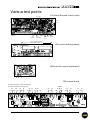
1
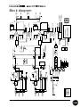
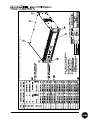
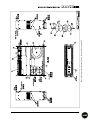
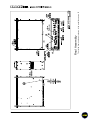
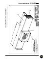
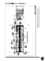
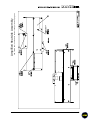
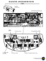
Go To Bulletins M2600 FR Series Power Amplifier SERVICE MANUAL 1998, 1999 MACKIE DESIGNS, INC. 820-180-00 Page 3 is interactive SERVICE ON THIS EQUIPMENT IS TO BE PERFORMED BY EXPERIENCED REPAIR TECHNICIANS ONLY 2 Click on any item to open that page CONTENTS INTRODUCTION ................................................................................. 3 Technical Support ........................................................................ 3 Disclaimer ....................................................................................... 3 BLOCK DIAGRAM ............................................................................. 4 SPECIFICATIONS ................................................................................ 5 TROUBLESHOOTING TIPS ............................................................... 6-7 RELIABILITY VERIFICATION ........................................................... 8-9 CIRCUIT THEORY ........................................................................ 10-13 ASSEMBLY DRAWINGS .............................................................. 14-19 PARTS LIST ................................................................................... 20-30 FOLD-OUT SECTIONS: schematics and pcb layouts Channel 1 .............................................................................. 129-1 Channel 2 .............................................................................. 130-1 Input board........................................................................... 131-1 Display board ........................................................................ 132-1 Power Distribution and in-rush limit ..................................... 133-1 Voltage Amp and protection ............................................ 170-1 Power Supply ........................................................................ 171-1 Output board ....................................................................... 172-1 15 V supply/Fan drive board ............................................. 186-1 INTRODUCTION ALL BOARDS SERVICE ON THIS EQUIPMENT IS TO BE PERFORMED BY EXPERIENCED REPAIR TECHNICIANS ONLY This manual contains basic service information. It is essential that you have a copy of the user’s manual as this contains the complete operating instructions. SERVICE TECHNICAL ASSISTANCE Mackie Designs, Service Technical Assistance, is available 8AM - 5PM PST, Monday through Friday for Authorized Mackie Service Centers, at 1-800-258-6883. Feel free to call with any questions and speak with a carefully-calibrated technician. If one is not available, leave a detailed message and a qualified Mackoid will return your call asap. DISCLAIMER The information contained in this manual is proprietary to Mackie Designs, Inc. The entire manual is protected under copyright and may not be reproduced by any means without express written permission from Mackie Designs, Inc. 3 4 MACKIE DESIGNS M•2600 BLOCK DIAGRAM 9/21/1998 THRU OUTPUT (XLR-MALE) LINE INPUT (XLR-FEMALE) LINE INPUT (1/4" TRS) THRU OUTPUT (XLR-MALE) LINE INPUT (XLR-FEMALE) LINE INPUT (1/4" TRS) FUSE LOW CUT FILTER FREQ LOW CUT FILTER FREQ LAMP POWER SWITCH TRANSFORMER THERMAL IN-RUSH LIMIT HIGH LOW 60-90-120Hz CROSSOVER THRU–LOW–HIGH CH 2 SIG HIGH LOW 60-90-120Hz CROSSOVER THRU–LOW–HIGH CH 1 SIG CH–2 TOROIDAL POWER TRANSFORMER IN-RUSH CONTROL LIMIT–OFF-LOW OUT Σ STEREO-MONO-BRIDGED 22 VAC -15 VDC +15 VDC + 30 VDC – + CH.1 100 VDC – + CH.2 100 VDC – STEREO-MONO-BRIDGED STEREO-MONO-BRIDGED (THE CHANNELS ARE SUMMED IN MONO OR BRIDGED MODE) LIMITER CONTROL CH–1 LIMIT–OFF-LOW OUT LIMIT–OFF-LOW OUT CH 2 TEMP SENSOR CH 1 TEMP SENSOR + CH.1 115 VDC – CH.1 DISSIPATION CH.2 DISSIPATION +115VDC –115VDC –100VDC +15VDC +15VDC +100VDC MUTE DC OFFSET PROTECT SHORT MUTE CHANNEL 1 POWER AMPLIFIER PROTECTION CIRCUITRY FUSE FUSE MUTE DC OFFSET PROTECT SHORT MUTE CHANNEL 2 POWER AMPLIFIER CH 2 SIG CH 1 SIG SHORT 2 0 FAN IDLE/VARIABLE CH.1 POWER DETECTOR FAN IDLE/VARIABLE CH.2 POWER DETECTOR 0 45 C – 65 C SPEED CONTROL CH.1 0 0 45 C – 65 C SPEED CONTROL CH.2 OL –3 –6 –9 –20 SIG COLD LED HOT LED CH.2 DISSIPATION PROTECT SHORT OL –3 –6 –9 –20 SIG CH.1 DISSIPATION METER DRIVE SHORT 1 PROTECT SHORT METER DRIVE VARIABLE SPEED FAN CONTROLLER OVER TEMPERATURE DETECTOR IN-RUSH CONTROL LOW VOLTAGE DETECT TRANSIENT SOA FLT STEADY STATE SOA FLT OUTPUT DISSIPATION OUTPUT STAGE CURRENT OUTPUT STAGE VOLTAGE PROTECTION CIRCUITRY FUSE FUSE IN-RUSH CONTROL LOW VOLTAGE DETECT TRANSIENT SOA FLT STEADY STATE SOA FLT OUTPUT DISSIPATION OUTPUT STAGE CURRENT OUTPUT STAGE VOLTAGE +30VDC -30VDC 22VAC LIMITER + CH.2 115 VDC – –115VDC –100VDC +15VDC +15VDC 22VAC LIMITER TRANSFORMER THERMAL SWITCH SHORT 1 SHORT 2 (THE SHORT LEDS ARE JOINED IN BRIDGED MODE) CH.2 GAIN INVERTER (FOR BRIDGED MONO OPERATION) CH.1 GAIN +115VDC +100VDC 0 1- 1+ 1- 1+ 1- 1+ + - + - FAN CH.2 MUTE 800C MUTE 0 52 C UN-MUTE 800 C MUTE CH.1 MUTE 52 C UN-MUTE OUTPUT RELAY OUTPUT RELAY CH. 2 SPEAKER OUT CH. 2 SPEAKON BRIDGED MONO SPEAKON CH. 1 SPEAKON CH. 1 SPEAKER OUT Block diagram Specifications Maximum Power at 1% THD, midband: 500 watts per channel into 8Ω 850watts per channel into 4Ω 1300 watts per channel into 2Ω 1700 watts into 8Ω bridged 2600 watts into 4Ω bridged Continuous Sine Wave Average Output Power, both channels driven: 425 watts per channel into 8Ω from 20Hz to 20kHz, with no more than 0.025% THD 700 watts per channel into 4Ω from 20Hz to 20kHz, with no more than 0.05% THD 1000 watts per channel into 2Ω from 20Hz to 20kHz, with no more than 0.1% THD 1,400 watts into 8Ω from 20Hz to 20kHz, with no more than 0.05% THD 2000 watts into 4Ω from 20Hz to 20kHz, with no more than 0.1% THD Note: Power ratings are specified at 120VAC line voltages. The M2600 power amplifier draws large amounts of current from the AC line with continuous sine wave testing. Accurate measurement of power requires a steady and stable AC supply. This means the line impedance must be very low to insure that the peak AC line voltage does not sag to less than 97% of its value. If driving highly reactive loads, we recommend that the limiter circuit be engaged. Power Bandwidth: 20Hz to 70kHz (+0, -3 dB) @ 700W into 4 Ω Frequency Response: 20Hz to 40kHz (+0, -1 dB) 10Hz to 70kHz (+0, -3 dB) Slew Rate: Voltage Slew Rate > 60V/µs Current Slew Rate> 30A/µs at 2Ω CMRR: > 40 dB, 20Hz to 20kHz Load Angle: 8(±jx) time independent at 8Ω 4(±jx) time dependent, T > 6 min. at 4Ω 2(1±jx) time dependent, T > 2 min. at 2Ω Transient Recovery: High Frequency Overload and Latching: No latch up at any frequency or level. High Frequency Stability: Unconditionally stable, driving any reactive or capacitive load. Turn On Delay: 3-5 seconds Variable Low-Cut Filter: 10Hz (Off) to 170Hz, 2nd-Order Bessel Internal Crossover: Switched: 60Hz/90Hz/120Hz, 4th-Order Linkwitz-Riley Lowpass outputs switchable to internal Subwoofer mode. Lowpass and Highpass outputs switchable to Thru output jacks. Limiter Section: Complementary Positive and Negative Peak Detecting Distortion: < 0.025% @ 8Ω < 0.050% @ 4Ω < 0.150% @ 2Ω Signal-to-Noise Ratio: > 107 dB below rated power into 4Ω Channel Separation: > 80 dB @ 1kHz Damping Factor: > 350 @ 400Hz Input Impedance: 24kΩ balanced Input Sensitivity: 1.23 volts (+4 dBu) for rated power into 4 ohms Gain: < 5µs < 1µs for 20 dB overdrive @ 1kHz Bridged mono operation: SMPTE IMD, TIM Rise Time: Indicators: 6 meter LEDs per channel SIG (Signal Present), -20, -9, -6, -3, OL (Overload) CH 1 & 2 PROTECT LEDs SHORT LEDs TEMP STATUS COLD/HOT LEDs Physical: (three rack spaces high, standard rack width) Height 5.20 inches (132mm) Front panel Width 19.00 inches (483mm) Chassis Width 17.24 inches (438mm) Depth 15.65 inches (398mm) Overall Depth 16.67 inches (423mm) Handle Depth 1.64 inches (42mm) Weight 55 pounds (25 kg) 32.7 dB (43V/V) Maximum Input Level: 9.75 volts (+22 dBu) 5 Troubleshooting Tips-output failures After a catastrophic failure, it is likely that some of the supply fuses will be blown. Check and replace any fuses on the 129, 130, 133, and 171 boards. Short across the Left most lead of R1 to the right most lead of R2 on the 133 board to short out the two 15W inrush resistors (see the diagram on the next page). Very slowly bring up the Variac while monitoring line consumption. It is likely that substantial line current will be pulled due to shorted output parts. If excessive current is not pulled, but a channel still stays in “protect” mode, the unit will still need repair. Remove the main heatsink sub-assembly from the unit and check for shorted output transistors. Once it has been determined which channel failed, remove it’s respective V-amp/ Protection board (055-170-00) to make access to the channel board easier. If one bad output is found, replace all 16 in the channel. When an output device shorts it can place high current stresses on the other output parts. These output parts can fail over time. Since long term reliability is paramount, please replace all the outputs. All 16 of the 3W 0.33Ω emitter resistors must be verified for proper value. Any off-tolerance, or open parts, need to be replaced. An off tolerance (higher resistance) emitter resistor will prevent it’s related output transistor from “doing it’s share” and will place more stress on it’s mates in the output section. Also verify the 16 base drive resistors (2.2Ω, 1/4W, fusible) are all OK. Verify that all eight drivers and that the pre-drivers are not shorted. If one driver is shorted replace it’s mates. Do the same with the pre-drivers. Also check all the resistors surrounding the drivers and predrivers. Measure the resistance between the “+I-sense” and “-I-sense” lines. The resistance should be 82.5Ω +/-5%. If this resistance is higher, check for open 33Ω fusible resistors on these lines. Take your time here looking to find all damaged parts: If one part is missed it still takes the same huge amount of time to disassemble the main heatsink assembly. After replacing the outputs, drivers, and pre-driver verify that the silicon transistor insulator wasn’t damaged (No shorts between collector legs and the heatsink). On the 170 board, check the VI limiters and detectors. It is not uncommon to damage these parts when the amplifier fails in a spectacular way! Look for shorts on Q24, Q25 or open R151 or R146. It is critical that these sections are working correctly. Shorted transistors can cause some odd asymmetrical clipping problems. Open parts will not allow the current limiting to operate effectively. If problems exist in these sections the amplifier might fail into a short, or might clip prematurely when loaded to 2 Ω. All of the above trouble shooting (not including part replacement) takes perhaps 30 to 45 minutes to do. If you take the time, and do all that is indicated above, it will allow 99% of the amplifiers to come up the first time! Trying to hurry, and skipping what is suggested, can lead to a frustrating and time consuming repair. Reassemble the main heatsink sub-assembly and plug the two power supply cables back into the 171 board (This can be done without installing the assembly back into the unit). Slowly bring up the supply and verify that line consumption isn’t excessive and that the output is centered (no DC offset). This can be measured on the “AMP-OUT” testpoint on the 170 board. It might be desirable to defeat the amplifier muting temporarily (Short “MUTE-VA” to “-15V-AMP” testpoints on the 170 board) so the channel is active even when the supplies are still very low. If the amp stays centered, power down the assembly and discharge the two main +/-100V supplies on both channels. Remove any temporary jumpers and reinstall the assembly into the chassis. Power the unit and verify that the repaired channel will pass a nice clean rail to rail sine wave. Next proceed to the “Reliability Verification” section on page 8. WARNING: FUSIBLE RESISTORS MUST ONLY BE REPLACED BY THE EXACT REPLACEMENT PARTS. ALWAYS CHECK THE PARTS LISTS TO VERIFY WHICH RESISTORS ARE THE FUSIBLE TYPE BEFORE REPLACING ANY RESISTORS IN THIS AMPLIFIER. 6 Various test points 170 board (Bias and check points) R146 Q24 Q25 R151 MUTE-VA J18 SOA POWER J19 -15V-AMP SOA TRANSIENT AMP BIAS OUT TEST BIAS ADJUST ADD A TEMPORARY SHORT (SEE TROUBLEHOOTING TIPS) 133 board (inrush bypassing) 186 board (fan speed adjustment) J1 J3 J2 R1 129 channel board BR= BASE RESISTOR (2.2 OHM, 1/4W FUSIBLE) ER= EMITTER RESISTOR (0.33 OHM, 3W) ER BR ER BR ER BR ER BR ER BR +I SENSE ER BR ER ER BR ER BR ER BR ER BR ER BR ER BR ER BR ER BR ER BR -I SENSE J6 +I SENSE 7 Reliability Verification Procedure After the unit has been repaired, the following should be done to assure long term reliable operation. If a distortion analyzer is present, distortion specifications should be verified. See the previous page for the 170 and 186 boards with some test points noted. 1. Adjust the bias control (R163 on 170 Board) in both channels for 12mV +/- 1mV measured at the bias test points (J23 along 170 board back edge) after unit has idled for a few minutes. This is with no signal and no load. The Pot and test points are clearly marked on both the top and bottom sides of the 170 board. With Full AC line voltage applied to unit, it will pull around 130W from the line (1.6A at 120V). Measure for DC offset on both output connectors, it should be less than +/- 50mV. 2. Verify and adjust the fan speed if needed. On the 186 board, short pin 1 to pin 2 on J3. Adjust R1 for 28V (+0V -1V) across J1 and J2. Remove the shorting jumper on J3. All the test points and pots are clearly labeled on the back side of the PCB and are easily accessed with the main heatsink sub-assembly installed. 3. Apply a 1KHz sine wave to the inputs and verify that the unloaded outputs have a waveform that is symmetrical and undistorted. Drive the outputs into clipping and carefully verify symmetrical “flat-topping” on the waveform. 4. Reduce the output levels, install a 0.1µF capacitor jumper from the output to ground connections, and verify that clipping behavior is proper. Verify that no high frequency oscillation occurs near and at clipping (parasitic oscillation). 5. Remove capacitive loading and minimize sine output. Verify and re-adjust the bias if required. Note that the bias will not drift appreciably in a unit that is functioning properly. 6. Connect the amplifier directly to the AC line and connect an 8Ω dummy load to both channels. Each 8Ω dummy load should have a minimum power rating of 500W. Bring the sine wave level up on both channels and verify symmetrical clipping. The output will clip somewhere between 150V - 180V pk/pk depending on how stiff the line is. Clipping should be as described above. Add the 0.1µF capacitive loading and verify clipping is still well behaved. 7. Individually load Channel 1 and Channel 2 with 2Ω . Each 2Ω dummy load should have minimum power rating of 1500W. Clipping should be symmetrical, well behaved , and occur somewhere around 120V - 140V pk/pk. Verify that clipping is well behaved after adding the 0.1µF capacitive loading. Reduce the output level to zero and remove the loading. 8. Next verify the two different short detectors. Perform these tests first on channel-1 and then repeat for channel-2. On the 170 board, short J18 pins 1 and 2 (this defeats the average power SOA detector and allows the transient SOA detector to be tested). Adjust the output level to 60V pk/pk and short the channel-1 output line. Channel-1’s front panel “short” and “protect” LEDs should turn on and the respective channel will mute for about 5 seconds. On the 170 board, remove the short on J18 and install a short on J19 pins 1 and 2 (this defeats the transient SOA detector and allows the average power SOA detector to be tested). Adjust the output level to 60V pk/pk and short the channel output line. Channel-1’s front panel “short” and “protect” LEDs should turn on and the respective channel will mute for about 5 seconds. Remove the shorting jumpers on channel-1 and repeat above testing on channel-2. 8 9. Place the amplifier in bridge mode and connect 4Ω loading to the bridge outputs (across both “+” output binding posts). The 4Ω dummy load should have a minimum power rating of 2000W. Slip some card stock between the heatsink-outlets and chassis sides to temporarily restrict the airflow. Monitor one of the outputs and adjust for a 60V pk/pk signal. Short across both outputs and verify that all four ‘Short” and “Protect” LEDs light and the amplifier mutes for 5 seconds. 10. Remove the short, monitor one of the outputs, and adjust for a 90V pk/pk sine output (1000W of output power bridged). After a few minutes the fan will begin running faster and faster (heatsink between 45°C and 65°C) and a short time later the amplifier will mute (heatsink at 80°C). The “Hot” and “protect” LEDs will come on. Remove the card stock and after a few minutes the amplifier will come out of mute mode and the “cold” LED will return. 11. Disconnect the loading and remove the input signals. Reconnect the amplifier to a Variac and confirm that the idle consumption is roughly 130W or 1.6A, as before. Connect the amplifier to speakers and verify that it sounds OK with music. 12. Perform the following leakage test before returning the amplifier to your customer: 1. Connect the amplifier under test to an AC power source using a ground-lift adaptor, leaving the amplifier’s safety ground floating. Turn the amplifier on. 2. Make a small loading RC circuit as shown in the diagram below, and connect the AC volt meter between the AC power source ground and any exposed metal on the unit under test. 3. The meter reading should be less than 750mV AC (note: this is equivalent to 0.5mA of leakage current). 4. Flip the plug over in the receptical so the hot and neutral are swapped. Verify that the reading is still less then 750 mV AC. 9 Circuit Theory Much of the circuitry in the M•2600 we hope is self explanatory from the schematics. This section will explain the unique circuits and architecture. Examples in this section will refer to Channel 1 for circuitry that is identical on both channels. INPUT CIRCUITRY The signal path begins with the INPUT BOARD (055-131-00). Following Channel 1’s input, signal is fed to a unity gain differential op-amp, U1A. The signal is next sent to U1B which serves as a 12dB/Oct. highpass filter. If not in SUBWOOFER mode, and if running in STEREO mode, the summing amp (U3B) and 24dB/Oct. Likwitz-Riley Crossover (U3A, U2, U4) are bypassed. The signal is sent via J11 to the gain control on the DISPLAY BOARD (055-132-00). After the gain control, the signal is buffered by U1A, returned to the INPUT BOARD and routed to the Channel-1 amplifier board via J6. Channel 2’s input signal path is electrically identical to Channel 1’s in STEREO mode. In PARALLEL MONO mode, Channel-1’s and Channel 2’s input signal is summed via U3B and is sent to both channel’s front panel level controls via SW3A and SW3B. For BRIDGE MONO operation, these summed inputs are sent to the channel-1 front panel level control which in turn feeds the channel-1 amplifier and also the inverter U10A. The output of U10A is routed to the channel-2 amplifier via SW3C. Also in BRIDGE mode, SW3D connects both channel-1’s and channel-2’s protection circuits together. The result being that when one amplifier detects a short circuit condition it will mute and immediately tell channel-2 to mute. Muting lasts around 5 seconds and the amplifier un-mutes until the next shorted condition is detected. The limiters (U6, U5, U7 and their associated components) are always in the signal path. When the limiter is switched off (via SW4) the LDR (Light Dependant Resistor) is in parallel with the source resistor (R39) and will not reduce signal amplitude. When the limiter is switched on, the LDR (U5B) is switched as a shunting element to ground. The Baker clamp in the power amplifier detects clipping and the LDR shunts away driving voltage until clipping almost disappears. This type of limiter is know as a feedback style (As opposed to feedforward style) of limiter. U6 is also used for the amplifier input slew clamps, comprised of local +/-5V supplies (D7, D8 and associated) and clamping diodes (D13 and D14). These diodes clamp the voltage feeding the power amp to around 10V pk/pk or about 6dB above the amplifier’s clipping point. This ultimately limits the risetime of the signal presented to the power amplifier, controlling commonmode conduction in the power amplifier output stage. Output from each crossover can be routed to the rear panel THRU jacks via SW2 and SW6. In the THRU position the THRU jack is hardwired to the input jacks. In LOW and HIGH output modes, the lowpass and highpass outputs of the crossover respectively are fed to the THRU jack. In these modes the output is impedance balanced via R28, R29 and R23. POWER AMPLIFIER CIRCUITRY The M•2600 use a class AB triple darlington output stage with complementary output devices. The output stage and the bias trackers are on the channel boards (129 and 130 boards) while the voltage amplifier and amplifier protection circuits are housed on two identical v-amp / protection (055-170-00) boards. Each channel has local main +/- 100V power supplies, and a +/ - 115V stacked supply for the front end circuitry. Each amplifier also has floating +/-16V supplies 10 that float along with the amplifier output line (D3 & D4 and associated parts on the 129 board). Common +/-15V supplies are shared throughout the product. Referring now to the 170 schematic: The amplifier is muted for 3 seconds on power up as C29 charges via R56. When this voltage has charged above 11.6V, U3C goes low turning on Q7, providing current for the differential pairs. The output of U3C, labeled “MUTE-VA”, when low turns on the Voltage Amplifier. Two seconds after MUTE-VA goes low, mute “MUTE-OP” goes low (Q27) closing the OutPut relay passing signal along to the output terminals. (Wait a minute! Differential Pairs? Read on…) An immediately obvious departure from standard designs is the Differentials and Symmetrical Voltage Amps. The reasoning behind this front end architecture is actually quite simple. Transistor transfer characteristics are not entirely linear, so even the best conventional front end design will introduce some distortion. Most amplifiers use negative feedback to reduce this problem (creating a few more in the process). Mackie FR Series amplifiers take a different approach. By using two complementary “mirror image” front end circuits, any distortion caused by non-linear transistor curves is effectively canceled out in the bias string, without feedback! Another design feature unique to Mackie FR Series Amplifiers is the Baker Clamp. The Baker Clamp has two functions; 1) Prevent output transistors saturating, 2) Drive the LIMITER LDR. Referring to the again to the 170 schematic: Q20 is a common base amplifier, it will turn on if Q2’s collector rises more than three diode drops above the +100V supply, preventing Q2’s collector from rising further. There are three diode drops between Q2’s collector and the base of pre-driver transistor (Q26 on 129 board). Once the output from the collector of Q2 makes it to the emitter of the output devices, there will be a total of six diode drops in series. Three “drops” up and six down: As a result, the output transistor emitters will never see a voltage greater than three diode drop below the +100V supply (even if the +100V supply fluctuates) and will never saturate. This will consequently remove saturation of the output stage, as a source common mode conduction. When the amplifier clips, Q20 and Q15 also send out “clipping pulses” at their collectors that is coincident with baker clamp conduction. These clipping pulses are crosscoupled to Q21 and Q22 and are stored in C47 and C51. These stored pulses allow for quick attack and slow release required by a peak limiter. Output from Q21 and Q22 is coupled to the LDR LED section via R110 and R152. PROTECTION CIRCUITS The M•2600 has several protection circuits in addition to main rail fuses on each channel. Circuits mute the amp if the output devices are loaded beyond their safe operating area (SOA). If there is DC on the output line, output relays open, disconnecting the load. The amplifier will also mute if the power transformer or main heatsink get too hot, if the input AC line voltage is low, or if either of the +/-15V supplies fails. Turn-On Inrush Current Limiter For the first second of operation there are two 15W power resistors (located on the 133 board) in series with the power transformer which eliminates what would otherwise be an extremely high turn-on current. After 1 second these resistors are shunted with a relay. This relay is turned on when the collector of Q26 (170 board) goes high. Note that either or both Q26’s on the two 170 boards can turn on this relay. 11 SOA protection There are two SOA detectors in the M-2600: One that monitors steady state output stage dissipation and one that monitors transient high current events. Both detectors need to monitor the output stage current. A voltage, representing output stage current, is derived by first sampling the voltage drop across the output transistor emitter resistors. These voltages are rectified via U9A R87, R88, R59 and R89. The rectified voltage is converted to a current via U9B, Q23, and associated. This current is referenced to the output line and must first be re-referenced to the +115V supply via Q14, D47 and associated. The current available at the connector of Q14 is converted to a voltage that is ground referenced via R138 and R162. This is buffered via U8A and adjusted via R162 such that 1 amp of output stage current is equal to 100mV of detected output. This current is compared to what represents a safe operating current at U4A (part of the transient SOA-Fault detector). If the current is greater than allowed for more than 10mS (Timing determined by R77 and C36), U4B sends out a fault indication which mutes the amplifier via U3C and associated, and fires the short led for 5.5 seconds (U3B and associated). While the output stage is quite tolerant of very high current demands for a very short time, it would destroy itself if it had to provide these currents on a long-term basis. The second detector actually looks at long-term dissipation in the output stage, and if excessive, will mute the amplifier. We already have a signal that is proportional to output stage current as described above. This signal is fed to one input of analog multiplier U7 via R80 and R84. U6A and U6B and their associated components look at the -100V supply and the amplifier output line. These voltages are converted to currents via R101, R129 and R130 and are rectified and summed such that for every volt between the output line and the supply rail, 100mV is presented as output. This second signal is presented to the other input of multiplier U7 via R133 and R82. Output from U7 is in the form of a current and is converted to a voltage via R136 and U8B. The gain of this multiplier is such that for 200 watts of output stage dissipation, 1 volt of output is obtained. The output of U8B is instantaneous power and is long-term averaged via R135 and C40. The cutoff of the filter is quite low in frequency, such that even a 20Hz signal on the amplifier output results in very little ripple voltage at C40. If the voltage on C40 is greater than 5V (equivalent to 1000W of output stage dissipation), U4C will toggle, muting the amplifier and firing the SHORT LED as above. Approximately 200mS of dissipation above 1000W is required to cause a fault. DC Fault Detection The amplifier output drives the subsonic lowpass filter of the DC fault detector (R154, C65 and C64). If the amplifier were to fail and short to the +100V rail, C64/C65 will charge to more that 5V in a few hundred milliseconds. Local +/-5.1V references on U2C and U2D set the threshold where: when the amplifier output voltage is “stuck” to greater than +/-5.1V, either comparator output will go low. This will open Q27, and in turn open the speaker relay on the respective channel board. When the amplifier is initialized, “MUTE-VA” is high and this biases C64/C65 above 5.1V via D14 and R36. This offset results in a delay of about 2 seconds from when the amplifier turns on (“MUTE-VA” low) and when the speaker relay closes. Low Voltage Detector D15, D2, and R7 supply a local 5V reference and are supplied current from the unregulated +30V supply via R32. 22VAC from the +/-30V windings is half-wave rectified via D26 and stored by C18. R53 limits the absolute peak current to protect D26. The voltage on C18 is divided down 12 via R33 and R8 and compared against the 5V reference at U3A. If the AC line voltage falls to around 60% of nominal (around 70VAC), the output of U3A goes low, resetting the mute and short monostables via D5 and D12. If the +15V supply fails, D3 and D4 bias the U3A inputs such that the amplifier is also muted. In the event of the -15V supply failing, R7 is no longer able to pull the anode of D15 low, and this also causes U3A to go low and mute the amplifier. THERMAL MANAGEMENT The T-Design Heatsink/Fan cools the output devices evenly and does not collect dust on the circuitry. The fan operates at variable speeds, controlled by output stage dissipation and temperature data supplied from both LM35DZ’s mounted on the heatsink. Fan Control Circuit Referring to the 186 board: The fan voltage comes from a feedback regulator circuit formed by U3B, Q2, Q1 and associated components. The fan supply is actually referenced to the -30V supply, so U3A and Q3 act to shift the ground-referenced control voltage “FAST-FAN” to a -30V supply reference. The output voltage of this regulator is adjusted via R1. D7 and C9 give the fan an initial full fan voltage “kick” (28V) to insure the fan starts spinning. The “FAST-FAN” control line varies from -1.6V (Slow) to -15V (Fast). Short J3 temporarily and adjust R1 for a voltage across the fan equal to 28V. Referring to the 170 board: The fan is never allowed to go faster than idle speed (Slow) unless the output stage dissipation is greater than 136 watts and the heatsink temperature is above 45°C. When the output stage dissipation is greater than 136W, U4D goes low. This eliminates D1 from supplying current to U2A. This decreases the reference voltage on U2A pin7, allowing it to work as a linear amplifier. With D1 conducting, U2A is effectively biased such that it’s output is high and the resulting fan speed is low. With 136W of output stage dissipation, U2A is allowed to linearly amplify the temperature sensor voltage on U1 via R2 and R5. C5, C15, C16, and C17 provide high frequency stability to this stage. The amplifier will linearly decrease the “FAST-FAN” voltage (increasing fan speed) between 45°C and 65°C. Above 65°C, U2A is saturated with the fan speed maximized. D11 isolates the Channel-1 and Channel-2 U2A circuits from each other. The connection of the U2A controllers is such that whichever channel is being used the hardest will determine the ultimate fan speed. Thermal Shutdown Heatsink temperature is sensed by U1 mounted to the main heatsink (one for each channel). The output of the sensor (10mV / °C) is compared to a 800mV reference at U2B. When the sensor is over 800mV (80°C) the output of U2B goes low, muting the amplifier via D27 and associated, and running the fan fast via D24. Hysteresis is built into the comparator via R3, such that the sensor voltage must reduce to 520mV (52°C) before the comparator goes back high and the amplifier un-mutes. A thermostat is built into the power transformer. If the power transformer temperature exceeds 130°C the thermostat closes and brings the “THERM” line to ground via Q1 and it’s associated parts on the 171 board. This shorts out the 800mV reference, and the U2B output goes low, muting the amplifier. Note that overheating of the power transformer is very unlikely but if it does occur, the amplifier will stay muted for over an hour before the transformer cools and the amplifier un-mutes itself. 13 The circled item numbers are shown in the parts list on page 20 Final Assembly 14 15 The circled item numbers are shown in the parts list on page 20 16 The circled item numbers are shown in the parts list on page 20 Final Assembly 17 The circled item numbers are shown in the parts list on page 21 Amplifier/Heatsink Assembly 18 The circled item numbers are shown in the parts list on page 21 Amplifier/Heatsink Assembly 19 The circled item numbers are shown in the parts list on page 21 Amplifier/Heatsink Assembly Master Parts List 090-078-00 M2600 Assembly, 120v Item# Part # 1 2 3 5 6 7 8 9 10 11 12 13 23 15 16 17 18 19 20 21 46 22 49 31 24 25 26 27 30 32 34 35 33 29 36 37 38 39 40 41 47 48 49 42 53 43 44 45 20 040-257-00 040-272-00 040-273-00 040-301-00 055-131-00-01 055-132-00-01 055-133-00-01 055-171-00-01 055-172-00-01 080-076-00 080-087-10 080-087-20 080-115-00 080-117-00 400-331-00 400-332-00 500-022-00 510-044-00 550-245-00 550-246-00 550-370-00 550-371-00 550-376-00 550-378-00 550-419-00 551-029-40 640-009-00 700-005-00 700-011-00 700-027-00 700-028-00 700-041-04 700-085-03 700-091-00 700-094-04 700-096-00 700-097-00 701-016-00 705-001-00 705-003-00 705-008-00 705-019-00 710-002-00 710-024-00 710-034-00 730-001-00 740-003-00 710-032-00 720-007-00 730-016-00 750-001-00 760-048-01 760-061-00 780-111-00 790-002-00 Description Rev Qty CBL ASSY 24GA 3P .098 6IN DIS 14G 1010 BRN 7.5 QDX2 DIS 14G 1010 BLU 6.5 QDX2 CBL ASSY SW PWR 23IN PCB ASSY INPUT - 2600 PCB ASSY DISPLAY M2600 PCB ASSY PWR DIST 120V PCB ASSY PWR SPLY M2600 PCB ASSY SPKR OUTPUT 2600 SA AMP M2600 SA HANDLE RIGHT M2600 SA HANDLE LEFT M2600 ASSY WIRE RCPT GND SA XFMR M2600 120V INSERT JACK BAN M-MAN RED INSERT JACK BAN M-MAN BLK SW RCKR ILLUMINATED FUSE SB 30A 3AB SCRN CHASSIS M2600 PNT SIDE RAIL RT- M2600 BRKT BRIDGE RECT HEATSINK BRKT XFMR MOUNT M2600 PNT COVER TOP M2600 PNT SIDE RAIL LT - M2600 FAB BRKT CBLE SHLD M2600 EXTR SCRN DSPLY BZL-M2600 LC IEC SJT 20A/125V 12AWG SEMS 8-32X1/2 PHP BLKZC MCH 4-40X1/4 BTNSKT BLKOX SEMS 8-32X3/8 PHP BLKZC SEMS 6-32X1/4 PHP BLKZC MCH 6-32X3/8 FL 100DG BLK SCR PHP M3X6 STL BLK ZC SEMS 8-32X3/4 PHP BLKZC MCH 4-40X3/8 82DEG FL BLK BOLT HEX 5/16X3-3/4 GR5 Z MCH 8-32X1/4 FL 82DG UCUT 5-20X5/16 PHPII TYP B BLK KEPNUT 6-32 NUT HEX-SPLD W/400-214-00 NUT LOCK 8-32 NUT STOVER LOCK 5/16X18 WASHER-SPLD W/400-214-00 WASH FLAT 5/16 HARD (USS) WASH STL .063X.344X.688 THERMAL JOINT COMPOUND TYRAP 8IN BLK WASH SHLD FIBRE .317X.750 TAPE DS 30MIL X 1.0W URTH LOCTITE 242 BUMPON ROUND BLK .63X.31 KNOB 9MM LT GRY KNOB VOLUME AMPS WASH RUB (W/TRANSFORMER) BAG POLY 12 X 18 2MIL B B A A A A2 A1 A A A6 A A A A A A A A B A A A A A A C A A A A B A A A A A A A A A A A A A A A A A A A A B A A A 1 1 1 1 1 1 1 1 1 1 1 1 1 1 AR AR 1 1 1 1 1 1 1 1 1 1 1 2 8 24 13 7 4 6 2 1 4 14 4 AR 2 1 AR 1 1 AR 4 1 AR AR 4 2 2 2 1 NOTE:The Item numbers in the first column of this page refer to the Final Assemby Drawings on pages 14-16 (transformer bracket) (transformer bolt) (transformer nut) (transformer bottom washer) (transformer top washer) (transformer shoulder washer) (transformer insulator washers) Item# Part # 790-022-00 800-087-00 800-107-00 810-076-00 810-082-00 820-078-00 Description Rev POLY-SHEET 52CF X 26 4MIL A BOX - M2600 A BOX SLEEVE M2600 A INSERT - M2600 A FOAM CORNER M2600 A OWN MANUAL M2600 ENG/DOM Qty 1 1 1 2 4 A 1 080-076-00 Amplifier/Heatsink subassembly Item Part# 1 2 3 5 34 33 7 8 9 10 11 12 13 14 15 16 17 18 19 20 22 23 24 25 33 26 27 29 30 080-076-00 040-263-00 055-129-00-01 055-130-00-01 055-170-00-02 055-186-00-01 080-116-00 410-013-00 410-014-00 550-368-00 550-372-00 550-373-00 550-377-00 550-393-00 550-403-00 550-420-00 550-421-00 551-045-00 700-005-00 700-010-04 700-028-00 700-034-00 700-087-00 700-088-00 700-110-00 705-008-00 710-020-00 710-036-00 710-044-00 730-001-00 730-025-00 740-003-00 740-011-00 780-123-00 780-133-00 Description Rev Qty SA AMP M2600 DIS 16GA 10C .165X2 19.5 PCB ASSY CHANNEL 1 - 2600 PCB ASSY CHANNEL 2 - 2600 PCB ASSY V-AMP PROT M2600 PCB ASSY PREDRV/FAN M2600 FAN ASSY M2600 SILPAD CUT M2600 NEW SILPAD CUT M2600 NEW COWLING HEATSINK M2600 BRKT FAN SHROUD M2600 BRKT SUPPORT PCB 28DEG BRKT TO-92 MOUNTING BRKT WIRE HARNESS M2600 FAB SEC HEATSINK M2600 FAB BRKT WIRE SHLD M2600 FAB BRKT VAMP SHLD M2600 FAB HEATSINK M2600 SEMS 8-32X1/2 PHP BLKZC TF 6-32X3/8 PHP BLKZC SEMS 6-32X1/4 PHP BLKZC SEMS 4-40X1/4 PHP BLKZC TF 4-40X5/8 TORX 1/4 WASH TF 4-40X5/8 TORX 3/8 WASH MCH 3-48X1/2 SKTCP SS NUT LOCK 8-32 WASH NO.4 COMPRESSION WASH FLT STL NO.4 .030THK WASH SHLDR TO-220 DELRIN THERMAL JOINT COMPOUND LOCTITE 222 TYRAP 8IN BLK HEATSHRINK TUBE 2:1 .50ID INSULATOR PCB M2600 INSULATOR VAMP SHLD M2600 A6 A A3 A2 A3 A2 A1 A A A A A A A A A A B A A B A A A A A A A A A A A B A A 1 2 1 1 2 1 1 1 1 1 1 2 2 1 2 1 1 1 4 14 5 5 23 33 22 4 44 22 22 AR AR 3 AR 1 1 NOTE: The Item numbers in the first column refer to the Amplfier/Heatsink Assemby Drawings on pages 17-19 21 055-129-00 Rev A Channel 1 board Part # Description Value Reference Designator 040-261-00 040-262-00 040-265-00 040-266-00 040-267-00 040-268-00 121-077-00 123-013-00 123-045-00 123-056-00 123-125-00 150-009-00 RIB 28GA TRAN 10C .1 3IN RIB 28GA TRAN 40C 3IN DIS 14GA BLK/ WHT 4.5IN QD DIS 14GA BLK/ WHT 6IN QDX2 DIS 14GA WHT 6IN QDX2 DIS 14GA BLKWHT 6IN QDX2 RESISTOR MOF RESISTOR MOF RESISTOR MOF RESISTOR MOF RES MO 3W 5% 15K OHM RES FUS .25W 5% 2.2 OHM 150 0.33 6.8 20 15K 2.2 5% 5% 5% 5% 5% 5% 150-037-00 RES FUS .25W 5% 33 OHM 33 5% 150-045-00 150-066-00 200-036-02 200-041-00 205-003-02 211-003-00 211-009-00 220-011-02 220-025-00 220-027-02 220-047-00 301-009-00 301-010-00 302-003-00 310-033-00 310-034-00 310-042-00 310-043-00 310-049-00 310-050-00 310-055-00 310-056-00 400-077-00 400-129-00 400-231-00 400-242-00 400-243-00 450-129-00 490-021-00 501-003-00 510-041-00 601-006-00 601-008-00 RES FUS .25W 5% 68 OHM 68 5% RESISTOR, FUSABLE, 1/4W 510 5% CAP, METALIZED POLY, T/R .1uF 10% CAPACITOR POLY HI-CURRENT 0.01 10% MICA 330PF 5% 500V 330pF 5% CER .001UF 10% 50V AX 0.001 10% CAPACITOR CERAMIC AXIAL 0.1 10% CAPACITOR LYTIC RADIAL T&R 100UF 10% CAPACITOR LYTIC RADIAL 1,000UF 10% CAPACITOR LYTIC RADIAL T&R 10UF 10% LYT 47UF 20% 160V RAD 47UF 20% DIODE POWER 1N4004 DIODE POWER 1N5404 DIODE ZENER 1N4745 TRANSISTOR PNP MJL21193 TRANSISTOR NPN MJL21194 TRANSISTOR NPN MJE15032 TRANSISTOR PNP MJE15033 XSTR PNP 2SA794A 2SA794A XSTR NPN 2SC1567A 2SC1567A XSTR NPN 2SA1480 2SA1480 XSTR PNP 2SC3790 2SC3790 HEADER STR LCK SHRD 20P .100 X 2 FUSE CLIP 0.25 DIA PC MNT HEADER, 2X5, MATE-N-LOCK CONNECTOR,STR,3P,.098 X 1,SHRD CONNECTOR,STR,2P,.098 X 1,SHRD PCB, M2600 CH-1 AMP MAGNET, .2THK .5DIA RELAY, SPDT T9AS5D12-24 FUSE 25A FB 3AG 25A INDUCTOR, AIR CORE 1uH 10% INDUCTOR 10uH J1 J6 J4 J12 J8 J9 R58 R40-55 R60-68 R59 R70-73 R3 R5-6 R8 R11 R13 R16 R18 R21 R23 R25 R29 R31 R33 R36 R38 R1 R4 R7 R9 R12 R14 R17 R19 R22 R24 R26-28 R30 R32 R34 R37 R39 R57 R69 R2 R10 R15 R20 R35 R56 R75 C22 C27 C24 C30-31 C1 C2 C4 C6 C8 C15 C17 C14 C16 C18 C20 C21 C25-26 C19 C23 D5 D1-2 D3-4 Q13-14 Q16-17 Q19-20 Q23-24 Q2-5 Q7-8 Q10-11 Q1 Q6 Q9 Q12 Q15 Q18 Q21 Q25 Q29 Q22 Q28 Q27 Q26 J5 Z1-4 J2 J3 J7 Z5 Z6 K1 F1-2 L1 L2-3 Components noted with this symbol shall be replaced only by the component specified.This is required to maintain product safety. 22 055-130-00 Rev A Channel 2 board Part # Description 040-262-00 040-269-00 040-270-00 121-077-00 123-013-00 123-045-00 123-056-00 123-125-00 150-009-00 RIB 28GA TRAN 40C 3IN DIS 14GA RED 6 IN QDX2 DIS 14GA BLKRED 6IN QDX2 RESISTOR MOF RESISTOR MOF RESISTOR MOF RESISTOR MOF RES MO 3W 5% 15K OHM RESISTOR, FUSABLE, 1/4W 150 0.33 6.8 20 15K 2.2 5% 5% 5% 5% 5% 5% 150-037-00 RES FUS .25W 5% 33 OHM 33 5% 150-045-00 150-066-00 200-036-02 200-041-00 205-003-02 211-003-00 211-009-00 220-011-02 220-027-02 220-047-00 301-009-00 301-010-00 302-003-00 310-033-00 310-034-00 310-042-00 310-043-00 310-049-00 310-050-00 310-055-00 310-056-00 400-077-00 400-129-00 400-173-00 RES FUS .25W 5% 68 OHM RESISTOR, FUSABLE, 1/4W CAP, METALIZED POLY, T/R CAPACITOR POLY HI-CURRENT MICA 330PF 5% 500V CER .001UF 10% 50V AX CAPACITOR CERAMIC AXIAL CAPACITOR LYTIC RADIAL T&R CAPACITOR LYTIC RADIAL T&R LYT 47UF 20% 160V RAD DIODE POWER DIODE POWER DIODE ZENER TRANSISTOR PNP TRANSISTOR NPN TRANSISTOR NPN TRANSISTOR PNP XSTR PNP 2SA794A XSTR NPN 2SC1567A XSTR NPN 2SA1480 XSTR PNP 2SC3790 HEADER STR LCK SHRD 20P .100 X FUSE CLIP 0.25 DIA PC MNT CONN QUICK DISC .250 W/STABLE-LOK TABS HEADER, 2X5, MATE-N-LOCK PCB M2600 CH-2 AMP MAGNET .200 THK X .50 DIA RELAY, SPDT FUSE 25A FB 3AG INDUCTOR, AIR CORE INDUCTOR STANDOFF, SWAGE, 4-40 X .312L 68 5% 510 5% .1uF 10% 0.01 10% 330pF 5% 0.001 10% 0.1 10% 100UF 10% 10UF 10% 47UF 20% 1N4004 1N5404 1N4745 MJL21193 MJL21194 MJE15032 MJE15033 2SA794A 2SC1567A 2SA1480 2SC3790 2 400-231-00 450-130-00 490-021-00 501-003-00 510-041-00 601-006-00 601-008-00 706-033-05 Value Reference Designator T9AS5D12-24 25A 1uH 10% 10uH J3 J5 J6 R60 R40-55 R61-69 R70 R58-59 R73-74 R2 R4 R7 R9 R11 R15 R17 R19 R22 R24 R27 R29 R32 R34-35 R37 R1 R3 R5 R8 R10 R12-14 R16 R18 R20 R23 R25 R28 R30 R33 R36 R38 R56-57 R6 R21 R26 R31 R39 R71 R75 C21 C26 C25 C29-30 C1 C7 C9 C11 C13 C15 C17 C14 C16 C18 C20 C23-24 C19 C22 D4 D1-2 D3 D5 Q15-16 Q18-19 Q21-24 Q2-3 Q6-7 Q9-10 Q12-13 Q1 Q5 Q8 Q11 Q14 Q17 Q20 Q25 Q29 Q4 Q28 Q27 Q26 J2 Z1-3 Z5 J4 J1 Z4 Z6 K1 F1-2 L1 L2-3 H1-4 H6 Components noted with this symbol shall be replaced only by the component specified.This is required to maintain product safety. 23 055-131-00-01 Rev A Input board Part # Description 040-258-00 040-259-00 040-260-00 100-027-00 130-062-02 140-078-00 140-082-00 140-089-00 140-090-00 140-095-00 140-123-00 145-318-00 145-331-00 145-346-00 145-389-00 145-397-00 DO NOT STUFF RIB 28GA TRAN 20C .1 5IN RIB 28GA TRAN 20C .1 6IN RIB 28GA TRAN 20C .1 20IN RESISTOR CF RES POT 12MM HORIZ DUAL RESISTOR TF SMT RES TF SM .1W 5% 2K4 OHM RESISTOR CF RES TF SM .1W 5% 5K1 OHM RES TF SM .1W 5% 8K2 OHM RES TF SM .1W 5% 100K OHM RESISTOR MF SMT RESISTOR MF SMT RESISTOR MF SMT RESISTOR MF RESISTOR MF 145-406-00 145-426-00 200-025-02 200-029-02 212-001-00 212-004-00 212-009-00 220-001-02 300-003-00 302-002-03 320-006-00 320-012-00 329-012-00 400-041-00 400-214-00 400-223-00 400-269-00 450-131-00 500-023-00 706-013-00 24 Value 120 50KC 1K6 2K4 4K7 5K1 8K2 100K 2K00 2K49 3K57 10K0 12K1 Reference Designator 5% 5% 5% 5% 5% 5% 5% 1% 1% 1% 1% 1% RESISTOR MF SMT 15K0 1% RESISTOR MF SMT 24K3 1% CAPACITOR MYLAR T&R 0.56 CAPACITOR MYLAR T&R 0.22 CAPACITOR CERAMIC SMT 0.01 10% CAPACITOR CERAMIC SMT 220PF 5% CAPACITOR CERAMIC SMT 47PF 5% CAPACITOR LYTIC RADIAL T&R 22UF 10% DIODE SIGNAL SMD DL4148 4.7V DL5230B OPAMP 2068E NJM 2068 OPAMP NJM4560M NJM4560M OPTO-ISOLATOR,LED/CDS VTL5C10 CONNECTOR XLR PC MTG VERT MALE CONNECTOR JACK 1/4” VERT PC MOUNT W/1MM LW CONNECTOR XLR PC MTG VERT FML TERM QDISC RTA .250 PCMT PCB, M-2600 INPUT SWITCH 4P3T STDF NO.4 X .978L M/F C22 C24 J6 J5 J11 R23 R28-29 R50-51 R65 R11 R66 R7 R67 R9 R69 R24-27 R52-53 R80-81 R8 R68 R77-79 R4 R6 R38-41 R72 R74 R35 R59 R14 R17 R44 R47 R3 R5 R21-22 R32 R56 R63-64 R71 R73 R1-2 R12-13 R16 R18 R30-31 R36-37 R42-43 R46 R48 R54-55 R60-61 R75-76 R20 R62 R15 R19 R33-34 R45 R49 R57-58 C10-11 C38-39 C12-13 C20-21 C28-29 C36-37 C4-5 C14-19 C23 C25 C30-35 C41-42 C3 C6-7 C40 C43-44 C1-2 C45-46 C8-9 C26-27 C47-48 D1-6 D9-16 D7-8 U1 U11 U2-4 U6 U8-10 U5 U7 J7 J10 J3 J12 J4 J13 J1 Z1 SW1-6 H1-2 055-132-00-01 Rev A Display board Part # Description Value 130-070-00 140-057-00 140-065-00 140-068-00 140-076-00 140-081-00 140-083-00 140-087-00 140-092-00 140-094-00 140-106-00 145-389-00 145-454-00 145-472-00 145-480-00 145-527-00 145-547-00 212-001-00 212-025-00 220-002-02 220-014-00 300-003-00 304-070-02 304-071-02 311-002-00 320-012-00 323-002-00 400-077-00 450-132-00 706-033-08 RESISTOR POT 9MM HORIZ 5KB 20% RESISTOR CF 220 5% RESISTOR CF 470 5% RESISTOR TF SMT 620 5% RESISTOR CF 1K3 5% RESISTOR CF 2K2 5% RESISTOR TF SMT 2K7 5% RESISTOR CF 3K9 5% RESISTOR CF 6K2 5% RESISTOR CF 7K5 5% RESISTOR TF SMT 24K 5% RESISTOR MF SMT 10K0 1% RESISTOR MF SMT 47K5 1% RESISTOR MF SMT 73K2 1% RES MF SM .1W 1% 88K7 OHM 88K7 1% RESISTOR MF SMT 274K 1% RESISTOR MF SMT 442K 1% CAPACITOR CERAMIC SMT 0.01 10% CAP CER .1UF 25V 10% X7R .1UF 10% CAPACITOR LYTIC RADIAL T&R 47UF 20% CAPACITOR LYTIC RADIAL KS 2.2UF 10% DIODE SIGNAL SMD DL4148 LED RED T1 W/.550 SPCR T/R RED LED GRN T1 W/.550 SPCR T/R GRN X-SISTOR PNP SMD IMBT4403 OPAMP NJM4560M NJM4560M I.C. QUAD COMPARATOR SMD LM339 HEADER STR LCK SHRD 20P .100 X 2 PCB, M2600 DISPLAY STANDOFF, SWAGE, 4-40 X .665L Reference Designator R2 R34 R17 R35 R41 R11 R24 R25 R43-49 R51 R1 R33 R12-13 R19-21 R50 R52 R16 R15 R18 R5 R10 R29 R31 R4 R7 R23 R27-28 R37 R39-40 R42 R8 R26 R3 R22 R14 R6 R9 R30 R32 R36 R38 C1 C3 C6 C10-11 C14 C19-20 C22-23 C7-9 C12-13 C15-16 C2 C4-5 C17 C18 C21 D13-20 D27 D1 D7 D21-22 D24-26 D2-6 D8-12 D23 Q1-2 U1 U6 U2-5 U7 J1 Z8 H1-3 H5-7 25 055-133-00-01 Rev A Power distribution 120V Part # Description 040-137-00 121-077-00 125-020-00 200-023-00 200-024-00 301-009-00 400-129-00 400-173-00 400-173-00 DIS 18GA GN/YL 96IN QD LUG RESISTOR MOF 150 5% RESISTOR WIRE WOUND 82 5% CAPACITOR, POLY BOX .001uF 20% CAPACITOR, POLY BOX .01uF 20% DIODE POWER 1N4004 FUSE CLIP 0.25 DIA PC MNT CONN QUICK DISC .250 CONN QUICK DISC .250 -00 AND -02 ASSY ONLY CONN QUICK DISC .250 -01 ASSY ONLY CONNECTOR,STR,3P,.098 X 1,SHRD PCB, M2600 PWR DISTRO & AC-INRUSH RELAY, SPDT T9AS5D12-24 FUSE 20A SLO-BLO -02 ASSY ONLY F1 FUSE 15A SLO-BLO -01 ASSY ONLY F1 FUSE 25A SLO-BLO -00 ASSY ONLY F1 400-173-00 400-242-00 450-133-00 501-003-00 510-017-00 510-018-00 510-033-00 Value Reference Designator J11 R3 R1-2 C1-2 C3-4 D1 Z1-2 J1-10 J12-15 J16-17 J18 J23 Z3 RL1 Z4 Z6 Z5 (100 VOLT MODELS ONLY) (240 VOLT MODELS ONLY) (120 VOLT MODELS ONLY) Components noted with this symbol shall be replaced only by the component specified.This is required to maintain product safety. 26 055-170-00 Rev A, Voltage amplifier and protection Part # Description Value Reference Designator 100-025-00 105-369-00 130-021-00 130-053-00 140-053-00 140-057-00 140-061-00 140-073-00 140-076-00 140-077-00 140-082-00 140-084-00 140-090-00 140-092-00 140-093-00 140-095-00 140-099-00 140-111-00 140-113-00 140-116-00 140-117-00 140-120-00 140-123-00 140-126-00 140-130-00 140-140-00 140-143-00 140-147-00 140-152-00 145-000-00 145-182-00 145-266-00 145-308-00 145-318-00 145-331-00 145-389-00 TEST POINT, PART OF PCB RESISTOR CF RES MF .125W 1% 6K19 OHM RESISTOR POT TRIM HORIZ RESISTOR POT TRIM HORIZ RESISTOR TF SMT RESISTOR TF SMT RES TF SM .1W 5% 330 OHM RES TF SM .1W 5% 1K0 OHM RES TF SM .1W 5% 1K3 OHM RESISTOR TF SMT RESISTOR TF SMT RESISTOR TF SMT RESISTOR TF SMT RES TF SM .1W 5% 6K2 OHM RES TF SM .1W 5% 6K8 OHM RESISTOR CF RESISTOR TF RESISTOR TF SMT RES TF SM .1W 5% 43K OHM RESISTOR TF SMT RESISTOR TF SMT RES TF SM .1W 5% 82K OHM RESISTOR TF SMT RESISTOR TF SMT RESISTOR TF SMT RESISTOR TF SMT RESISTOR TF SMT RESISTOR TF SMT RESISTOR TF SMT RES TF SM .1W 0 OHM RESISTOR MF SMT RESISTOR MF SMT RES MF SM .1W 1% 1K58 OHM RESISTOR MF SMT RESISTOR MF SMT RESISTOR MF SMT 100 6K19 10KB 200 150 220 330 1K0 1K3 1K5 2K4 3K0 5K1 6K2 6K8 8K2 12K 36K 43K 56K 62K 82K 100K 150K 200K 510K 680K 1M 1M6 0 76.8 576 1K58 2K00 2K49 10K0 5% 1% 145-414-00 145-418-00 RESISTOR MF SMT RESISTOR MF SMT 18K2 20K0 1% 1% 145-422-00 145-426-00 RES MF SM .1W 1% 22K1 OHM RESISTOR MF SMT 22K1 24K3 1% 1% 145-427-00 145-435-00 145-439-00 145-469-00 145-531-00 RESISTOR MF SMT RES MF SM .1W 1% 30K1 OHM RESISTOR MF SMT RESISTOR MF SMT RESISTOR MF SMT 24K9 30K1 33K2 68K1 301K 1% 1% 1% 1% 1% 5% 5% 5% 5% 5% 5% 5% 5% 5% 5% 5% 5% 5% 5% 5% 5% 5% 5% 5% 5% 5% 5% 5% 5% 5% 5% 1% 1% 1% 1% 1% 1% J1-9 J11-16 J24-26 R11 R30 R37-38 R141-144 R162 R163 R12-13 R22-23 R6 R159 R16 R19 R160 R105 R104 R140 R156 R103 R139 R48-49 R53 R77 R86 R102 R110 R152 R121 R7 R47 R51 R41-42 R67-68 R97-98 R10 R26 R57 R76 R122 R120 R158 R59 R88 R155 R147 R150 R45 R60 R123 R148-149 R3 R31 R36 R54 R107 R116 R1 R101 R106 R126 R129-130 R8 R55-56 R108 R115 R28 R9 R33 R92 R5 R15 R20 R40 R43 R93-94 R99-100 R145 R112 R114 R46 R14 R21 R39 R44 R63 R72 R146 R151 R157 R52 R64 R71 R111 R50 R58 R61-62 R73-74 R124 R128 R136 R138 R83 R132 R25 R29 R32 R34-35 R75 R78-80 R82 R84 R127 R133 R137 R119 R125 R2 R4 R65-66 R69-70 R90-91 R95-96 R109 R117 R113 R118 R17-18 R24 R27 R87 R89 R135 R161 R81 R85 R131 R134 R153-154 27 055-170-00 Rev A, continued Part # Description Value 200-011-02 200-036-02 205-006-02 210-017-02 212-001-00 212-006-00 212-007-00 CAPACITOR MYLAR T&R CAP, METALIZED POLY, T/R MICA 30PF 5% 500V T/A CAPACITOR, CERAMIC, T/R CER .01UF 10% 50V X7R SM CAPACITOR CERAMIC SMT CAPACITOR CERAMIC SMT 0.0022 .1uF 30pF 470pF 0.01 470PF 0.047 5% 10% 5% 5%/Y5E 10% 5% 5% 212-008-00 212-016-00 212-018-00 212-019-00 212-025-00 212-029-00 220-001-02 220-004-02 220-014-00 300-003-00 CER .22UF +80/-20% 25V SM CAPACITOR CERAMIC SMT CAPACITOR CERAMIC SMT CER 150PF 5% 50V SM CAP CER .1UF 25V 10% X7R CAPACITOR CERAMIC SMT CAPACITOR LYTIC RADIAL T&R CAPACITOR LYTIC RADIAL T&R CAPACITOR LYTIC RADIAL KS DIODE SIGNAL SMD 0.22 1000PF 10PF 150PF .1UF 270PF 22UF 470UF 2.2UF DL4148 5% 5% 5% 5% 10% 5% 10% 10% 10% 300-010-00 302-009-00 302-010-03 310-042-00 310-043-00 311-001-00 311-002-00 311-007-00 311-008-00 311-009-00 311-010-00 311-011-00 311-012-00 311-019-00 311-020-00 320-012-00 323-002-00 329-014-00 329-036-03 400-143-00 400-171-00 400-186-00 450-170-00 550-369-00 601-008-00 712-021-01 DIODE SIGNAL SMD RLS245 DIODE ZENER SMD DL5260B DIODE ZENER SMD DL5232 XSTR NPN MJE15032 MJE15032 XSTR PNP MJE15033 MJE15033 X-SISTOR NPN SMD IMBT4401 X-SISTOR PNP SMD IMBT4403 TRANSISTOR PNP SMD 2SA1415 TRANSISTOR NPN SMD 2SC3645 TRANSISTOR PNP SMD 2SA1552 TRANSISTOR NPN SMD 2SC4027 TRANSISTOR PNP SMD 2SA1740 TRANSISTOR NPN SMD 2SC4548 TRANSISTOR PNP SMD 2SB792 TRANSISTOR NPN SMD 2SD814 OPAMP NJM4560M NJM4560M I.C. QUAD COMPARATOR SMD LM339 IC, DEG C TEMP SENSOR LM35DZ NJM4200M ANLG MULTR SM NJM4200 CONN, HDR, 3-PIN, UN-SHROUDED 0 .100 CONN, HDR, 2-PIN, UN-SHROUDED, 0 .100 CONN HDR 40P .100 X 2 STR SHRD PCB, M2600 V-AMP & PROTECTION BRACKET, L INDUCTOR 10uH RIVET 28 Reference Designator C59 C31-32 C60 C45 C20 C25 C46 C4 C6 C8-10 C12-13 C22-23 C27 C30 C33 C35 C37-39 C41-42 C52-58 C61-62 C1 C3 C47 C51 C63 C5 C21 C24 C43-44 C11 C14 C15-18 C66 C34 C7 C48-49 C64-65 C50 C2 C19 C26 C28-29 C36 C40 D1-6 D11-14 D16-25 D27-36 D38-39 D41-42 D44-45 D47-52 D56-57 D26 D37 D40 D43 D46 D53-55 D58-60 D7 D10 D8-9 D15 Q1 Q2 Q13 Q22 Q25 Q7-8 Q21 Q24 Q28 Q4 Q9-10 Q20 Q3 Q11-12 Q15 Q6 Q26 Q5 Q27 Q14 Q23 Q16-17 Q18-19 U5-6 U8-9 U2-4 U1 U7 J21-22 J17-20 J23 J10 Z1 H1-2 L1-2 Z4-7 055-171-00-01 Rev A Power supply board Part # Description Value Reference Designator 100-077-00 123-109-00 150-037-00 200-036-02 211-009-00 220-006-00 220-029-00 220-041-00 300-001-00 301-009-00 301-010-00 301-015-00 310-007-00 400-060-00 400-133-00 400-173-00 RES CF .125W 5% 15K OHM RESISTOR MOF RESISTOR, FUSABLE, 1/4W CAP, METALIZED POLY, T/R CAPACITOR CERAMIC AXIAL CAPACITOR LYTIC RADIAL CAPACITOR LYTIC RADIAL CAPACITOR LYTIC RADIAL DIO SIG 1N4148 100V 500MW DIODE POWER DIODE POWER DIODE BRIDGE XSTR NPN 2N4401 FUSE CLIP PCMT 5MM DIA HEADER, 2X3, MATE-N-LOCK CONN QUICK DISC .250 W/STABLE-LOK TABS HEADER, 2X5, MATE-N-LOCK PCB, M2600, POWER SUPPLY FUSE 5X20 15K 5% 3.3K 5% 33 5% .1uF 10% 0.1 10% 2200UF 10% 2200UF 20% 15,000uF20% 1N4148 1N4004 1N5404 25A 2N4401 R10-12 R1-8 R9 C15-22 C23-24 C9-12 C13-14 C1-8 D19-20 D1-5 D10-16 D6-9 D17-18 Q1 Z1-3 Z5 J6 J3-5 400-231-00 450-171-00 510-026-00 T-3.15A J1-2 Z4 F1-2 055-172-00-01 Rev A Speaker output board Part # Description Value 400-138-01 400-173-00 400-237-00 450-172-00 SPEAKONS HORIZ 4 CKT CONN QUICK DISC .250 W/STABLE-LOK TABS CONNECTOR, QUAD BANANA PCB, M2600, OUTPUT Reference Designator J2-4 J5-8 J1 Z1 Components noted with this symbol shall be replaced only by the component specified.This is required to maintain product safety. 29 055-186-00 Rev A 15 Volt supply/fan drive board Part # 100-031-00 100-049-00 100-056-00 100-061-00 100-066-00 100-068-00 100-069-00 100-073-00 100-078-00 100-080-00 100-090-00 100-097-00 121-081-00 130-021-00 211-009-00 220-001-02 220-027-02 300-001-00 301-009-00 310-002-00 310-024-00 310-050-00 320-011-00 321-001-00 321-002-00 400-078-00 400-171-00 450-186-00 550-369-00 601-013-00 712-021-01 30 Description Value TEST POINT, PART OF PCB RESISTOR CF 180 5% RESISTOR CF 1K 5% RESISTOR CF 2K 5% RESISTOR CF 3K3 5% RESISTOR CF 5K1 5% RES CF .125W 5% 6K2 OHM 6K2 5% RESISTOR CF 6K8 5% RESISTOR CF 10K 5% RESISTOR CF 16K 5% RESISTOR CF 20K 5% RES CF .125W 5% 51K OHM 51K 5% RESISTOR CF 100K 5% RESISTOR MF 2K2 5% RESISTOR POT TRIM HORIZ 10KB CAPACITOR CERAMIC AXIAL 0.1 10% CAPACITOR LYTIC RADIAL T&R 22UF 10% CAPACITOR LYTIC RADIAL T&R 10UF 10% DIODE SIGNAL 1N4148 DIODE POWER 1N4004 TRANSISTOR PNP 2N4403 TRANSISTOR PNP 2SB817 TRANSISTOR NPN 2SC1567A I.C. LINEAR NJM 4560 I.C. LINEAR NEG 3 TERM VOLTAGE LM 7915 REGULATOR I.C. LINEAR POS 3 TERM VOLTAGE LM 7815 REGULATOR CONNECTOR STR LCK SHRD 10P .100 X 2 CONN, HDR, 2-PIN, UN-SHROUDED, 0 .100 PCB, M2600, +/-15V SUPPLY & FAN DRIVE BRACKET, L CHOKE, POWER AXIAL 470uH RIVET Reference Designator J1-2 R8 R7 R10 R6 R2 R5 R4 R9 R3 R13 R12 R11 R14 R1 C3 C5 C7-8 C2 C4 C9 C1 C6 D5-7 D1-4 Q3 Q1 Q2 U3 U1 U2 J4 J3 Z1 H1-2 L1-2 Z4-7 M•2600 amplifier modification instructions Models affected: All M•2600 amplifiers with serial numbers “AU” or those less than DX10017. Add this mod as part of your normal repair procedures. Symptom: No signal, dead channel or distorted output. Possible Cause: 1: 2: Transistor Q5 on the V-amp protection boards may be shorted to an adjacent trace. Transistors Q3 and Q4 on the V-amp protection boards may oscillate under certain conditions, causing V-amp board failure, and/or failure of R57 on Ch.1 amp board and R56 on CH.2 amp board (33Ω fuse). Solution: Rework both V-amp circuit boards (055-170-00) as follows: 1: 2: Replace Q5 with a new transistor and make sure it is postioned further down, away from the trace, or : cut two traces and add a jumper wire (to bypass any possiblity of a short). Replace R14, R15, R20 and R21 with new value resistors (to improve the reliability of the final class A stage, comprising of transistors Q1 to Q6 and associated resistors, diodes and caps). Safety Warning: Caution! These instructions are for use by qualified personnel only. To avoid electric shock, do not perform any servicing unless you are qualified to do so. Refer all service to qualified personnel. Tools Required: Sharp pointed X-acto knife, Phillips screwdriver, Torx and Allen drivers, needle nose pliers, safety glasses, soldering iron suitable for surface mount work. Parts Required: Insulated jumper wire 311-010-00 2SC4027 Transistor, NPN, SMD Q5 140-057-00 220Ω Resistor, 0.1W, 5%, Thick film, SMT 0805 R15 and R20 140-084-00 3KΩ Resistor, 0.1W, 5%, Thick film, SMT 0805 R14 and R21 Procedure: (The following modifications must be performed on both V-amp boards) 1/ 2/ 3/ 4/ 5/ 6/ 7/ 8/ 9/ Remove all cords (including the power cable and speaker outputs) from the amplifier. Remove the amplifier subassembly from the chassis. Remove the two V-amp boards (055-170-00) from the amplifier subassembly. Replace R15 and R20 (from 0Ω to 220Ω). Replace R14 and R21 (from 2kΩ to 3kΩ). Follow step A, or follow step B, whichever you find easiest. A/ If you have a new transistor in stock, replace Q5 and make sure it is positioned further down, so the left leg is fully on its pad and not over the trace. Note: a new transistor is required because unsoldering and repositioning the original transistor will thermal-stress and weaken the part. B/ Carefully cut the trace in two places on each board. See the diagram on the second page. The trace should be cut exactly in the locations shown. It is not easy to get to, and you may have to scrape off some of the white silkscreen lines in order to see the trace. Solder a jumper wire in the position shown, on each board. Reassemble the V-amp boards onto the amplifier subassembly. Reassemble the amplifier subassembly into the chassis. Perform a complete specification and safety test. Refer to the service manual for details. M•2600 modification SSE July 2000 M2600mod.pdf, page 1 of 2 THE MACKIE FIXER MACKIE DESIGNS SERVICE NEWS Amplifier Subassembly 055-170-00 V-AMP board Solder here Change R14 and R15 Cut trace here Cut trace here Change R20 and R21 Solder an insulated wire here M•2600 modification SSE July 2000 M2600mod.pdf, page 2 of 2