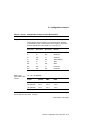
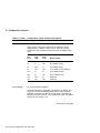
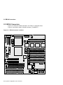
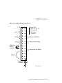
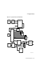
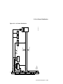
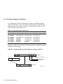
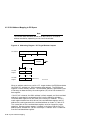
1
Digital Semiconductor 21164 Alpha
Microprocessor Evaluation Board
User’s Guide
Order Number: EC–QD2UD–TE
Revision/Update Information:
Digital Equipment Corporation
Maynard, Massachusetts
This document supersedes the
Alpha 21164 Microprocessor Evaluation
Board User’s Guide (EC–QD2UC–TE).
March 1996
Possession, use, or copying of the software described in this publication is authorized only
pursuant to a valid written license from Digital or an authorized sublicensor.
While Digital believes the information included in this publication is correct as of the date of
publication, it is subject to change without notice.
Digital Equipment Corporation makes no representations that the use of its products in the
manner described in this publication will not infringe on existing or future patent rights, nor do
the descriptions contained in this publication imply the granting of licenses to make, use, or sell
equipment or software in accordance with the description.
© Digital Equipment Corporation 1996.
All rights reserved.
Printed in U.S.A.
Alpha AXP, AlphaGeneration, DEC, DECchip, DECladebug, Digital, Digital Semiconductor, VAX
DOCUMENT, the AlphaGeneration design mark, and the DIGITAL logo are trademarks of
Digital Equipment Corporation.
Digital Semiconductor is a Digital Equipment Corporation business.
Digital UNIX Version 3.2 for Alpha is a UNIX 93 branded product.
Hewlett-Packard is a registered trademark of Hewlett-Packard Company.
IEEE is a registered trademark of The Institute of Electrical and Electronics Engineers, Inc.
Intel and UPI are trademarks of Intel Corporation.
Motorola is a registered trademark of Motorola, Inc.
National is a registered trademark of National Semiconductor Corporation.
NT and Windows NT are trademarks of Microsoft Corporation.
Powerview is a trademark of Viewlogic Systems, Inc.
TI is a registered trademark of Texas Instruments Inc.
TriQuint is a registered trademark of TriQuint Semiconductor, Inc.
UNIX is a registered trademark in the United States and other countries, licensed exclusively
through X/Open Company Ltd.
VxWorks is a registered trademark of Wind River Systems, Inc.
Xilinx is a trademark of Xilinx Incorporated.
All other trademarks and registered trademarks are the property of their respective owners.
This document was prepared using VAX DOCUMENT Version 2.1.
Contents
About This Guide . . . . . . . . . . . . . . . . . . . . . . . . . . . . . . . . . . . . . . . . . . . .
ix
1 Introduction to the EB164
1.1
1.1.1
1.1.2
1.1.3
1.1.4
1.1.5
1.1.6
1.1.7
1.1.8
1.2
System Components and Features . . . . . . . . . . . . . .
Digital Semiconductor 21171 Core Logic Chipset
Memory Subsystem . . . . . . . . . . . . . . . . . . . . . .
L3 Bcache Subsystem Overview . . . . . . . . . . . . .
PCI Interface Overview . . . . . . . . . . . . . . . . . . .
ISA Interface Overview . . . . . . . . . . . . . . . . . . .
Miscellaneous Logic . . . . . . . . . . . . . . . . . . . . . .
Software Support . . . . . . . . . . . . . . . . . . . . . . . .
Design Support . . . . . . . . . . . . . . . . . . . . . . . . .
Evaluation Board Uses . . . . . . . . . . . . . . . . . . . . . .
.
.
.
.
.
.
.
.
.
.
.
.
.
.
.
.
.
.
.
.
.
.
.
.
.
.
.
.
.
.
.
.
.
.
.
.
.
.
.
.
.
.
.
.
.
.
.
.
.
.
.
.
.
.
.
.
.
.
.
.
.
.
.
.
.
.
.
.
.
.
.
.
.
.
.
.
.
.
.
.
.
.
.
.
.
.
.
.
.
.
.
.
.
.
.
.
.
.
.
.
1–1
1–3
1–3
1–3
1–4
1–4
1–4
1–5
1–6
1–6
Configuration Jumpers . . . . . . . . . . . . . . . . . . . . . . . . . . . . . . . . .
EB164 Connectors . . . . . . . . . . . . . . . . . . . . . . . . . . . . . . . . . . . .
2–1
2–8
2 System Configuration and Connectors
2.1
2.2
3 Functional Description
3.1
3.2
3.2.1
3.2.2
3.3
3.4
3.4.1
3.4.2
3.5
3.5.1
3.5.2
EB164 Bcache Interface . . . . . . . . . . .
Digital Semiconductor 21171 Chipset .
CIA Chip Overview . . . . . . . . . . .
DSW Overview . . . . . . . . . . . . . . .
Main Memory Interface . . . . . . . . . . .
PCI Devices . . . . . . . . . . . . . . . . . . . .
Saturn-IO (SIO) Chip . . . . . . . . . .
PCI Expansion Slots . . . . . . . . . .
ISA Bus Devices . . . . . . . . . . . . . . . . .
Combination Controller . . . . . . . .
Keyboard and Mouse Controller . .
.
.
.
.
.
.
.
.
.
.
.
.
.
.
.
.
.
.
.
.
.
.
.
.
.
.
.
.
.
.
.
.
.
.
.
.
.
.
.
.
.
.
.
.
.
.
.
.
.
.
.
.
.
.
.
.
.
.
.
.
.
.
.
.
.
.
.
.
.
.
.
.
.
.
.
.
.
.
.
.
.
.
.
.
.
.
.
.
.
.
.
.
.
.
.
.
.
.
.
.
.
.
.
.
.
.
.
.
.
.
.
.
.
.
.
.
.
.
.
.
.
.
.
.
.
.
.
.
.
.
.
.
.
.
.
.
.
.
.
.
.
.
.
.
.
.
.
.
.
.
.
.
.
.
.
.
.
.
.
.
.
.
.
.
.
.
.
.
.
.
.
.
.
.
.
.
.
.
.
.
.
.
.
.
.
.
.
.
.
.
.
.
.
.
.
.
.
.
.
.
.
.
.
.
.
.
.
.
.
.
.
.
.
.
.
.
.
.
.
.
.
.
.
.
.
.
.
.
.
.
.
3–2
3–4
3–4
3–6
3–6
3–7
3–8
3–8
3–8
3–10
3–11
iii
3.5.3
3.5.4
3.5.5
3.6
3.7
3.8
3.9
3.10
3.11
3.11.1
3.11.2
3.11.3
3.11.4
Time-of-Year Clock . . . . . . .
Utility Bus Memory Device
ISA Expansion Slots . . . . .
Interrupts . . . . . . . . . . . . . . . .
System Clocks . . . . . . . . . . . . .
Reset and Initialization . . . . . .
Serial ROM . . . . . . . . . . . . . . .
dc Power Distribution . . . . . . .
System Software . . . . . . . . . . .
Serial ROM Code . . . . . . . .
Mini-Debugger Code . . . . .
Debug Monitor ROM Code .
Operating Systems . . . . . . .
.
.
.
.
.
.
.
.
.
.
.
.
.
.
.
.
.
.
.
.
.
.
.
.
.
.
.
.
.
.
.
.
.
.
.
.
.
.
.
.
.
.
.
.
.
.
.
.
.
.
.
.
.
.
.
.
.
.
.
.
.
.
.
.
.
.
.
.
.
.
.
.
.
.
.
.
.
.
.
.
.
.
.
.
.
.
.
.
.
.
.
.
.
.
.
.
.
.
.
.
.
.
.
.
.
.
.
.
.
.
.
.
.
.
.
.
.
.
.
.
.
.
.
.
.
.
.
.
.
.
.
.
.
.
.
.
.
.
.
.
.
.
.
.
.
.
.
.
.
.
.
.
.
.
.
.
.
.
.
.
.
.
.
.
.
.
.
.
.
.
.
.
.
.
.
.
.
.
.
.
.
.
.
.
.
.
.
.
.
.
.
.
.
.
.
.
.
.
.
.
.
.
.
.
.
.
.
.
.
.
.
.
.
.
.
.
.
.
.
.
.
.
.
.
.
.
.
.
.
.
.
.
.
.
.
.
.
.
.
.
.
.
.
.
.
.
.
.
.
.
.
.
.
.
.
.
.
.
.
.
.
.
.
.
.
.
.
.
.
.
.
.
.
.
.
.
.
.
.
.
.
.
.
.
.
.
.
.
.
.
.
.
.
.
.
.
.
.
.
.
.
.
.
.
.
.
.
.
.
.
.
.
.
.
.
.
.
.
.
.
.
.
.
.
.
.
.
.
.
.
.
.
.
.
.
.
.
.
3–11
3–12
3–12
3–13
3–16
3–19
3–21
3–22
3–24
3–24
3–24
3–25
3–25
Physical Memory Regions . . . . . . . . . . . . . . . . . . . . . . . . . . . . . .
21164 Address Mapping to PCI Space . . . . . . . . . . . . . . . . . . . . .
Cacheable Memory Space (00.0000.0000 Through
00.3FFF.FFFF) . . . . . . . . . . . . . . . . . . . . . . . . . . . . . . . . . . . .
PCI Sparse Memory Space (80.0000.0000 Through
85.7FFF.FFFF) . . . . . . . . . . . . . . . . . . . . . . . . . . . . . . . . . . . .
Hardware Extension Registers (HAE) . . . . . . . . . . . . . . . . . .
PCI Sparse I/O Space (85.8000.0000 Through
85.FFFF.FFFF) . . . . . . . . . . . . . . . . . . . . . . . . . . . . . . . . . . .
PCI Dense Memory Space (86.0000.0000 Through
86.FFFF.FFFF) . . . . . . . . . . . . . . . . . . . . . . . . . . . . . . . . . . .
PCI Configuration Space (87.0000.0000 Through
87.1FFF.FFFF) . . . . . . . . . . . . . . . . . . . . . . . . . . . . . . . . . . . .
PCI Interrupt Acknowledge/Special Cycle Space
(87.2000.0000 Through 87.3FFF.FFFF) . . . . . . . . . . . . . . . . .
EB164 Hardware-Specific and Miscellaneous Register Space
(87.4000.0000 Through 87.6FFF.FFFF) . . . . . . . . . . . . . . . . .
PCI-to-Physical Memory Addressing . . . . . . . . . . . . . . . . . . .
4–1
4–4
4 System Address Mapping
4.1
4.2
4.2.1
4.2.2
4.2.3
4.2.4
4.2.5
4.2.6
4.2.7
4.2.8
4.2.9
4–5
4–5
4–9
4–10
4–13
4–14
4–19
4–19
4–20
5 Power and Environmental Requirements
5.1
5.2
5.3
iv
Power Requirements . . . . . . . . . . . . . . . . . . . . . . . . . . . . . . . . . .
Environmental Requirements . . . . . . . . . . . . . . . . . . . . . . . . . . .
Physical Board Parameters . . . . . . . . . . . . . . . . . . . . . . . . . . . . .
5–1
5–2
5–2
A I/O Space Address Maps
A.1
PCI Sparse Memory Space . . . . . . . . . . . . . . . . . . . . . . . . . .
A.2
PCI Sparse I/O Space . . . . . . . . . . . . . . . . . . . . . . . . . . . . . .
A.2.1
PCI Sparse I/O Space—Region A . . . . . . . . . . . . . . . . . .
A.2.1.1
PC87312 Combination Controller Register Address
Space . . . . . . . . . . . . . . . . . . . . . . . . . . . . . . . . . . . .
A.2.1.2
8242AH Keyboard and Mouse Controller Addresses
A.2.1.3
Time-of-Year (TOY) Clock Addresses . . . . . . . . . . . .
A.2.1.4
Flash ROM Segment Select Register . . . . . . . . . . . .
A.2.1.5
Configuration Jumpers (CONF4—CONF15) . . . . . .
A.2.1.6
Interrupt Control PLD Addresses . . . . . . . . . . . . . .
A.2.2
PCI Sparse I/O Space—Region B . . . . . . . . . . . . . . . . . .
A.3
PCI Dense Memory Space . . . . . . . . . . . . . . . . . . . . . . . . . .
A.3.1
Flash ROM Memory Addresses . . . . . . . . . . . . . . . . . . .
A.3.2
Map of Flash ROM Memory . . . . . . . . . . . . . . . . . . . . . .
A.3.3
Flash ROM Configuration Registers . . . . . . . . . . . . . . . .
A.4
PCI Configuration Address Space . . . . . . . . . . . . . . . . . . . .
A.4.1
SIO PCI-to-ISA Bridge Configuration Address Space . . .
A.5
PCI Interrupt Acknowledge/Special Cycle Address Space . .
A.6
Hardware-Specific and Miscellaneous Register Space . . . . .
A.6.1
CIA Main CSR Space . . . . . . . . . . . . . . . . . . . . . . . . . . .
A.6.2
CIA Memory Control CSR Space . . . . . . . . . . . . . . . . . .
A.6.3
CIA PCI Address Translation Map Space . . . . . . . . . . . .
A.7
21164 Alpha Microprocessor Cbox IPR Space . . . . . . . . . . . .
....
....
....
A–1
A–1
A–2
.
.
.
.
.
.
.
.
.
.
.
.
.
.
.
.
.
.
.
.
.
.
.
.
.
.
.
.
.
.
.
.
.
.
.
.
.
.
.
.
.
.
.
.
.
.
.
.
.
.
.
.
.
.
.
.
.
.
.
.
.
.
.
.
.
.
.
.
.
.
.
.
.
.
.
.
A–2
A–6
A–6
A–7
A–8
A–8
A–8
A–13
A–13
A–13
A–14
A–16
A–16
A–18
A–18
A–18
A–19
A–20
A–22
.
.
.
.
.
.
.
.
.
.
.
.
.
.
.
.
.
.
.
.
.
.
.
.
.
.
.
.
.
.
.
.
.
.
.
.
.
.
.
.
.
.
.
.
.
.
.
.
.
.
.
.
.
.
.
.
B–1
B–2
B–4
B–4
B–6
B–6
B–6
B–8
B–8
B–8
B–9
B–12
B–15
B–16
B SROM Initialization
B.1
B.2
B.3
B.4
B.5
B.5.1
B.5.2
B.5.3
B.6
B.7
B.8
B.9
B.10
B.11
SROM Initialization . . . . . . . . . . . . . . . . . . .
Firmware Interface . . . . . . . . . . . . . . . . . . .
Automatic CPU Speed Detection . . . . . . . . .
CPU Bus Interface Timing . . . . . . . . . . . . . .
Bcache Read and Write Timing Calculations
Read Cycle Calculation . . . . . . . . . . . . .
Write Cycle Calculations . . . . . . . . . . . .
Read/Write Spacing Calculations . . . . . .
Memory Initialization . . . . . . . . . . . . . . . . .
Bcache Initialization . . . . . . . . . . . . . . . . . .
Special ROM Header . . . . . . . . . . . . . . . . . .
Flash ROM Structure . . . . . . . . . . . . . . . . . .
Flash ROM Access . . . . . . . . . . . . . . . . . . . .
Icache Flush Code . . . . . . . . . . . . . . . . . . . .
.
.
.
.
.
.
.
.
.
.
.
.
.
.
.
.
.
.
.
.
.
.
.
.
.
.
.
.
.
.
.
.
.
.
.
.
.
.
.
.
.
.
.
.
.
.
.
.
.
.
.
.
.
.
.
.
.
.
.
.
.
.
.
.
.
.
.
.
.
.
.
.
.
.
.
.
.
.
.
.
.
.
.
.
.
.
.
.
.
.
.
.
.
.
.
.
.
.
.
.
.
.
.
.
.
.
.
.
.
.
.
.
.
.
.
.
.
.
.
.
.
.
.
.
.
.
.
.
.
.
.
.
.
.
.
.
.
.
.
.
.
.
.
.
.
.
.
.
.
.
.
.
.
.
.
.
.
.
.
.
.
.
.
.
.
.
.
.
v
C Technical Support and Ordering Information
C.1
C.2
C.3
C.4
Obtaining Technical Support . . . . . . . . . . .
Ordering Digital Semiconductor Products .
Ordering Digital Semiconductor Literature
Ordering Third-Party Literature . . . . . . . .
.
.
.
.
.
.
.
.
.
.
.
.
.
.
.
.
.
.
.
.
.
.
.
.
.
.
.
.
.
.
.
.
.
.
.
.
.
.
.
.
.
.
.
.
.
.
.
.
.
.
.
.
.
.
.
.
.
.
.
.
.
.
.
.
.
.
.
.
C–1
C–1
C–3
C–4
EB164 Functional Block Diagram . . . . . . . . . . . . . . . . .
EB164 Jumper Locations . . . . . . . . . . . . . . . . . . . . . . . .
Configuration Jumpers . . . . . . . . . . . . . . . . . . . . . . . . . .
EB164 Connector Locations . . . . . . . . . . . . . . . . . . . . . .
Detail of Header Connector J2 . . . . . . . . . . . . . . . . . . . .
EB164 Bcache Array . . . . . . . . . . . . . . . . . . . . . . . . . . .
Main Memory Interface . . . . . . . . . . . . . . . . . . . . . . . . .
ISA Devices . . . . . . . . . . . . . . . . . . . . . . . . . . . . . . . . . .
Interrupt Logic . . . . . . . . . . . . . . . . . . . . . . . . . . . . . . . .
System Clocks and Distribution . . . . . . . . . . . . . . . . . . .
System Reset and Initialization . . . . . . . . . . . . . . . . . . .
SROM and Serial Port . . . . . . . . . . . . . . . . . . . . . . . . . .
dc Power Distribution . . . . . . . . . . . . . . . . . . . . . . . . . .
PCI Sparse Memory Space Address
Translation—Region 1 . . . . . . . . . . . . . . . . . . . . . . . . . .
PCI Sparse Memory Space Address
Translation—Region 2 . . . . . . . . . . . . . . . . . . . . . . . . . .
PCI Sparse Memory Space Address
Translation—Region 3 . . . . . . . . . . . . . . . . . . . . . . . . . .
PCI Sparse I/O Space Address Translation—Region A . .
PCI Sparse I/O Space Address Translation—Region B . .
Addressing Diagram: PCI Target Window Compare . . .
PCI to System Bus Scatter-Gather Address Translation
Map . . . . . . . . . . . . . . . . . . . . . . . . . . . . . . . . . . . . . . . .
Board Component Layout . . . . . . . . . . . . . . . . . . . . . . .
.
.
.
.
.
.
.
.
.
.
.
.
.
.
.
.
.
.
.
.
.
.
.
.
.
.
.
.
.
.
.
.
.
.
.
.
.
.
.
.
.
.
.
.
.
.
.
.
.
.
.
.
1–2
2–2
2–3
2–8
2–9
3–2
3–5
3–9
3–14
3–17
3–20
3–22
3–23
....
4–8
....
4–9
Glossary
Index
Figures
1–1
2–1
2–2
2–3
2–4
3–1
3–2
3–3
3–4
3–5
3–6
3–7
3–8
4–1
4–2
4–3
4–4
4–5
4–6
4–7
5–1
vi
.
.
.
.
.
.
.
.
.
.
.
.
.
.
.
.
4–9
4–12
4–12
4–22
....
....
4–25
5–3
B–1
B–2
Write Cycle Timing . . . . . . . . . . . . . . . . . . . . . . . . . . . . . . . .
Special Header Content . . . . . . . . . . . . . . . . . . . . . . . . . . . . .
B–6
B–9
Tables
1–1
2–1
2–2
3–1
3–2
3–3
4–1
4–2
4–3
4–4
4–5
4–6
4–7
4–8
4–9
4–10
4–11
4–12
4–13
4–14
5–1
5–2
A–1
A–2
A–3
A–4
A–5
A–6
A–7
Main Memory Sizes . . . . . . . . . . . . . . . . . . . . . . . . . . . . . .
Configuration Jumper Position Descriptions . . . . . . . . . . .
EB164 Connector Descriptions . . . . . . . . . . . . . . . . . . . . . .
Bcache Configurations . . . . . . . . . . . . . . . . . . . . . . . . . . . .
EB164 System Interrupts . . . . . . . . . . . . . . . . . . . . . . . . .
PCI-to-ISA SIO Bridge Interrupts . . . . . . . . . . . . . . . . . . .
Three Physical Memory Regions . . . . . . . . . . . . . . . . . . . .
Physical Memory Regions (Detailed) . . . . . . . . . . . . . . . . .
PCI Sparse Memory Space Byte-Enable Generation . . . . .
INT4_VALID to Address Translation for Sparse Write
Operations . . . . . . . . . . . . . . . . . . . . . . . . . . . . . . . . . . . .
High-Order Sparse Space Bits . . . . . . . . . . . . . . . . . . . . . .
PCI Sparse I/O Space Byte-Enable Generation . . . . . . . . .
PCI Configuration Space Definition . . . . . . . . . . . . . . . . . .
PCI Configuration Space Byte-Enable Generation . . . . . . .
CPU Address Encoding for PCI Device Selection . . . . . . . .
EB164 Primary PCI IDSEL Mapping . . . . . . . . . . . . . . . .
Hardware-Specific Register Space . . . . . . . . . . . . . . . . . . .
PCI Target Window Enables . . . . . . . . . . . . . . . . . . . . . . .
PCI Target Address Translation—Direct Mapped (SG
Mapping Disabled) . . . . . . . . . . . . . . . . . . . . . . . . . . . . . .
Scatter-Gather Map Address . . . . . . . . . . . . . . . . . . . . . . .
Power Supply dc Current Requirements . . . . . . . . . . . . . .
Board Component List . . . . . . . . . . . . . . . . . . . . . . . . . . . .
PC87312 Combination Controller Register Address Space
Map . . . . . . . . . . . . . . . . . . . . . . . . . . . . . . . . . . . . . . . . . .
Keyboard and Mouse Controller Addresses . . . . . . . . . . . .
Time-of-Year Clock Device Addresses . . . . . . . . . . . . . . . . .
Flash ROM Segment Select Register . . . . . . . . . . . . . . . . .
Configuration Jumpers (CONF4—CONF15) . . . . . . . . . . .
Interrupt Control PLD Addresses . . . . . . . . . . . . . . . . . . .
SIO PCI-to-ISA Bridge Operating Register Address Space
Map . . . . . . . . . . . . . . . . . . . . . . . . . . . . . . . . . . . . . . . . . .
.
.
.
.
.
.
.
.
.
.
.
.
.
.
.
.
.
.
1–3
2–4
2–10
3–3
3–13
3–15
4–2
4–3
4–7
.
.
.
.
.
.
.
.
.
.
.
.
.
.
.
.
.
.
4–7
4–8
4–11
4–16
4–17
4–18
4–19
4–20
4–21
.
.
.
.
.
.
.
.
4–23
4–24
5–1
5–4
.
.
.
.
.
.
.
.
.
.
.
.
A–2
A–6
A–7
A–7
A–8
A–8
..
A–9
vii
A–8
A–9
A–10
A–11
A–12
A–13
A–14
A–15
A–16
B–1
B–2
B–3
B–4
B–5
B–6
viii
Flash ROM Memory Addresses (Within Segment) . . . . . . .
Map of Flash ROM Memory . . . . . . . . . . . . . . . . . . . . . . . .
Flash ROM Configuration Registers . . . . . . . . . . . . . . . . . .
Address Bits and PCI Device IDSEL Pins . . . . . . . . . . . . .
SIO PCI-to-ISA Bridge Configuration Address Space Map .
CIA Control, Diagnostic, and Error Registers . . . . . . . . . .
CIA Memory Control Registers . . . . . . . . . . . . . . . . . . . . .
PCI Address Translation Registers . . . . . . . . . . . . . . . . . .
21164 Alpha Microprocessor Cache Configuration
Registers . . . . . . . . . . . . . . . . . . . . . . . . . . . . . . . . . . . . . .
Output Parameter Descriptions . . . . . . . . . . . . . . . . . . . . .
Cache Loop Delay Characteristics . . . . . . . . . . . . . . . . . . .
Typical SRAM Specifications . . . . . . . . . . . . . . . . . . . . . . .
CPU Specifications . . . . . . . . . . . . . . . . . . . . . . . . . . . . . . .
Special Header Entry Descriptions . . . . . . . . . . . . . . . . . .
Flash ROM Image Selection . . . . . . . . . . . . . . . . . . . . . . . .
.
.
.
.
.
.
.
.
.
.
.
.
.
.
.
.
A–13
A–13
A–15
A–16
A–17
A–18
A–19
A–20
.
.
.
.
.
.
.
.
.
.
.
.
.
.
A–22
B–2
B–4
B–5
B–5
B–10
B–12
About This Guide
This guide describes Digital Semiconductor’s 21164 Alpha Microprocessor
Evaluation Board (also called the EB164), an evaluation and development
module for computing systems based on the 21164 Alpha Microprocessor and
the Digital Semiconductor 21171 core logic chipset.
Audience
This guide is intended for system designers and others who use the EB164 to
design or evaluate computer systems based on the 21164 microprocessor and
21171 chipset.
Scope
This guide describes the features, configuration, functional operation, and
interfaces of the EB164. This guide does not include specific bus specifications
(for example, PCI or ISA buses). Additional information is available in the
EB164 schematics, program source files, and appropriate vendor and IEEE
specifications. See Appendix C for information about how to order related
documentation and obtain additional technical support.
Content
This guide contains the following chapters and appendixes:
•
Chapter 1, Introduction to the EB164, is an overview of the EB164,
including its components, uses, and features.
•
Chapter 2, System Configuration and Connectors, describes the user
environment configuration; board connectors and functions; jumper
functions; and identifies jumper and connector locations.
•
Chapter 3, Functional Description, provides a functional description of
the board, including the 21171 chipset, L3 backup cache (Bcache) and
memory subsystems, systems interrupts, clock and power subsystems,
ix
and peripheral component interconnect (PCI) and Industry Standard
Architecture (ISA) devices.
•
Chapter 4, System Address Mapping, describes the mapping of the 40-bit
processor address space into memory and I/O space addresses.
•
Chapter 5, Power and Environmental Requirements, describes the board
power and environmental requirements, and identifies major board
components.
•
Appendix A, I/O Address Maps, lists the physical EB164 PCI address
spaces and regions, including control, I/O interface, and address operating
registers and PCI/ISA device registers.
•
Appendix B, SROM Initialization, describes the general serial readonly memory (SROM), Bcache, and memory initialization steps and
associated parameters. Also included are the firmware interface, timing
considerations, and SROM header information.
•
Appendix C, Technical Support and Ordering Information, describes how to
obtain Digital Semiconductor information and technical support, and how
to order Digital Semiconductor products and associated literature.
•
Glossary lists and defines terms associated with the EB164.
Document Conventions
This section provides the conventions used in this document.
Bit and Field Abbreviations
The following list describes the bit and field abbreviations:
Bit/Field
Abbreviation
Description
RO (read only)
Bits and fields specified as RO can be read but not written.
RW (read/write)
Bits and fields specified as RW can be read and written.
WO (write only)
Bits and fields specified as WO can be written but not read.
Bit Notation
Multiple bit fields are shown as extents (see Ranges and Extents in this
section).
Caution
Cautions indicate potential damage to equipment or data.
x
Data Units
The following data unit terminology, common within Digital, is used throughout
this guide:
Term
Words
Bytes
Bits
Word
1
2
16
Longword
2
4
32
Quadword
4
8
64
Octaword
8
16
128
Hexword
16
32
256
Note
Notes provide additional information.
Numbering
All numbers are decimal or hexadecimal unless otherwise indicated. In case
of ambiguity, a subscript indicates the radix of nondecimal numbers. For
example, 19 is a decimal number, but 1916 and 19A are hexadecimal numbers.
UNPREDICTABLE and UNDEFINED
Throughout this manual, the terms UNPREDICTABLE and UNDEFINED are
used. Their meanings are quite different and must be carefully distinguished.
In particular, only privileged software (that is, software running in kernel
mode) can trigger UNDEFINED operations. Unprivileged software cannot
trigger UNDEFINED operations. However, either privileged or unprivileged
software can trigger UNPREDICTABLE results or occurrences.
UNPREDICTABLE results or occurrences do not disrupt the basic operation
of the processor. The processor continues to execute instructions in its normal
manner. In contrast, UNDEFINED operations can halt the processor or cause
it to lose information.
The terms UNPREDICTABLE and UNDEFINED can be further described as
follows:
•
UNPREDICTABLE
–
Results or occurrences specified as UNPREDICTABLE might vary from
moment to moment, implementation to implementation, and instruction
to instruction within implementations. Software can never depend on
results specified as UNPREDICTABLE.
xi
–
An UNPREDICTABLE result might acquire an arbitrary value subject
to a few constraints. Such a result might be an arbitrary function of
the input operands or of any state information that is accessible to the
process in its current access mode. UNPREDICTABLE results may be
unchanged from their previous values.
Operations that produce UNPREDICTABLE results might also produce
exceptions.
–
An occurrence specified as UNPREDICTABLE might happen or not
based on an arbitrary choice function. The choice function is subject
to the same constraints as are UNPREDICTABLE results and, in
particular, must not constitute a security hole.
Specifically, UNPREDICTABLE results must not depend upon, or be
a function of the contents of memory locations or registers that are
inaccessible to the current process in the current access mode.
Also, operations that might produce UNPREDICTABLE results must
not:
•
Write or modify the contents of memory locations or registers to
which the current process in the current access mode does not have
access.
•
Halt or hang the system or any of its components.
For example, a security hole would exist if some UNPREDICTABLE
result depended on the value of a register in another process, on
the contents of processor temporary registers left behind by some
previously running process, or on a sequence of actions of different
processes.
•
xii
UNDEFINED
–
Operations specified as UNDEFINED can vary from moment to
moment, implementation to implementation, and instruction to
instruction within implementations. The operation can vary in effect
from nothing, to stopping system operation.
–
UNDEFINED operations can halt the processor or cause it to lose
information. However, UNDEFINED operations must not cause the
processor to hang, that is, reach an unhalted state from which there
is no transition to a normal state in which the machine executes
instructions. Only privileged software (that is, software running in
kernel mode) can trigger UNDEFINED operations.
Data Field Size
The term INTnn, where nn is one of 2, 4, 8, 16, 32, or 64, refers to a data field
of nn contiguous NATURALLY ALIGNED bytes. For example, INT4 refers to a
NATURALLY ALIGNED longword.
Ranges and Extents
Ranges are specified by a pair of numbers separated by two periods ( .. ) and
are inclusive. For example, a range of 0..4 includes the integers 0, 1, 2, 3, and
4.
Extents are specified by a single number, or a pair of numbers in angle
brackets ( < > ) separated by a colon ( : ) and are inclusive. For example,
bits <7:3> specify an extent including bits 7, 6, 5, 4, and 3.
Register and Memory Figures
Register figures have bit and field position numbering starting at the right
(low-order) and increasing to the left (high-order).
Memory figures have addresses starting at the top and increasing toward the
bottom.
Schematic References
Logic schematics are included in the EB164 design package. In this guide,
references to schematic pages are printed in italics. For example, the following
specifies schematic page 3:
‘‘. . . the 26.66-MHz oscillator (eb164.3) supplies . . .’’
In some cases, more than one schematic page is referenced. For example, the
following specifies schematic pages 10 through 13:
‘‘. . . the data switches (eb164.10–13) . . .’’
Signal Names
Signal names in text are printed in boldface lowercase type. For example,
‘‘ . . . bits data<127:0> are delivered to the Bcache SIMM connectors . . . ’’
xiii
1
Introduction to the EB164
This chapter provides an overview of the EB164, its components, features, and
uses.
The Digital Semiconductor 21164 Alpha Microprocessor Evaluation Board
(EB164) is an evaluation and development module for computing systems
based on the Digital Semiconductor 21164 Alpha microprocessor and the
Digital Semiconductor 21171 core logic chipset.
The EB164 provides a single-board hardware and software development
platform for the design, integration, and analysis of supporting logic and
subsystems. The board also provides a platform for PCI I/O device hardware
and software development.
Appendix C provides ordering information and a list of related documentation.
1.1 System Components and Features
The EB164 is implemented in industry-standard parts and uses a 21164
CPU running at 266 MHz (supports 300 MHz and 333 MHz). The functional
components are shown in Figure 1–1 and are introduced in the following
subsections.
Introduction to the EB164 1–1
1.1 System Components and Features
Figure 1–1 EB164 Functional Block Diagram
Index
Digital Semiconductor
21164 Alpha
Microprocessor
19
Control
Bcache
SIMM
Sockets (X2)
Bcache Tag
10
Data
128
Check
16
Digital Semiconductor
21171 Core Logic Chipset
Digital Semiconductor
21171−BA
Data Switch
(X4)
Control
Address
Commands
37
Data
64
Digital Semiconductor
21171−CA
Control, I/O Interface,
and Address
PCI−to−ISA
Bridge
Support
− Oscillator
− Serial ROM
256
Data
DRAM
SIMM
Sockets
(X8)
Address/Control
3 Dedicated PCI Slots
2 Dedicated ISA Slots
1 Shared PCI/ISA Slot
Flash ROM
Time−of−Year
Keyboard/Mouse
Combination
Controller
2 IDE Devices
Diskette
Parallel Port
2 Serial Ports
MK−2306−01A
1–2 Introduction to the EB164
1.1 System Components and Features
1.1.1 Digital Semiconductor 21171 Core Logic Chipset
The 21164 is supported by the 21171 chipset. The chipset consists of the
following two application-specific integrated circuit (ASIC) types:
•
One copy of the 21171-CA control, I/O interface, and address chip (CIA)
provides the interface between the 21164, main memory (addressing and
control), and the peripheral component interconnect (PCI) bus. It also
provides the data switch companion chips with control information to direct
the data flow.
•
Four copies of the 21171-BA data switch chip (DSW) provide the memory
interface data path and route PCI data through the CIA chip.
The chipset includes the majority of functions required to develop a highperformance PC or workstation, requiring minimum discrete logic on the
module. It provides flexible and generic functions to allow its use in a wide
range of systems.
1.1.2 Memory Subsystem
The dynamic random-access memory (DRAM) provides 32MB to 512MB with
a 256-bit data bus. The memory is contained in one bank of eight commodity
single inline memory modules (SIMMs). Single- or double-sided SIMMs may
be used. Each SIMM is 36 bits wide, with 32 data bits and 4 check bits,
with 70 ns or less access. Table 1–1 lists the SIMM sizes supported and the
corresponding main memory size for 256-bit arrays.
Table 1–1 Main Memory Sizes
SIMM Size
2 36
2 36
4M 2 36
8M 2 36
16M 2 36
Eight SIMMs (256-Bit Array)
1M
32MB
2M
64MB
128MB
256MB
512MB
1.1.3 L3 Bcache Subsystem Overview
The board-level external L3 backup cache (Bcache) subsystem supports
multiple cache sizes and access times. Cache sizes supported are 2MB with
Alpha cache SIMMs populated with 128K 2 8 SRAMs, and 4MB and 8MB
with SIMMs populated with 512K 2 8 SRAMs. Speeds of 6 ns to 15 ns can
be used. Wave pipelining decreases the cache loop times by one CPU cycle in
Introduction to the EB164 1–3
1.1 System Components and Features
most cases. The Bcache size can be reconfigured through onboard hardware
jumpers. As implemented in the EB164, the Bcache operates in 64-byte mode
only.
1.1.4 PCI Interface Overview
The EB164 PCI interface is the main I/O bus for the majority of functions
(SCSI interface, graphics accelerator, and so on). The PCI interface provides a
selectable PCI speed between 25 MHz and 33 MHz (based on the 21164 clock
divisor). An onboard PCI-to-ISA bridge is provided through an Intel 82378ZB
Saturn-I/O chip (SIO).
The PCI bus has three dedicated PCI expansion slots (one 64-bit and two
32-bit) and one shared 64-bit PCI/ISA slot.
1.1.5 ISA Interface Overview
The ISA bus has two dedicated slots and a third shared ISA/PCI slot. It
provides the following system support functions:
•
Mouse and keyboard controller functions—provided by an Intel 8242 chip.
•
An IDE interface, a diskette controller, two universal asynchronous
receiver–transmitters (UARTs) with full modem control, and a bidirectional
parallel port—provided by a National 87312 combination chip.
•
A time-of-year (TOY) function—provided by a Dallas Semiconductor
DS1287 chip.
•
Operating system support—provided by a 1MB flash ROM that contains
firmware and debug monitor code.
Users can develop code on a host system, and load software into the EB164
through a serial line, diskette, or Ethernet board. In addition, sectors of
the flash ROM can be programmed for application-specific purposes.
1.1.6 Miscellaneous Logic
The EB164 contains the following miscellaneous components:
•
Clocks
A 26.66-MHz oscillator and phase-locked loop (PLL) clock generator provide
a clock source to the 21164 microprocessor and system.
A 14.3-MHz crystal and frequency generator provide a clock source for ISA
devices.
•
Serial ROM
1–4 Introduction to the EB164
1.1 System Components and Features
A Xilinx XC17128 serial ROM (SROM) contains initial code that is loaded
into the 21164 instruction cache (Icache) on power-up. A serial line
interface is also provided to allow direct connection to a terminal line for
debugging purposes.
•
Programmable array logic (PAL) devices for the following functions:
One PAL for utility bus (Ubus) decoding
One PAL for interrupts
Two PAL devices for memory row address strobe (RAS) bank generation
and buffering
1.1.7 Software Support
Software support code, consisting of a debug monitor and Windows NT ARC
firmware is contained in a 1MB flash ROM. Development code can be generated
on a host system and loaded into the EB164 through a serial line, an Ethernet
board, or a diskette. In addition, sectors of the flash ROM can be programmed
for an application-specific purpose. Source code for the debug monitor, serial
ROM power-up code, and example PALcode is provided in the Alpha Evaluation
Board Software Developer’s Kit (EBSDK). The monitor provides functions that
allow you to:
•
Download files through serial and Ethernet ports and diskette.
•
Load data from a ROM through the debug monitor.
•
Examine and deposit the EB164 system registers, a few 21164 internal
processor registers (IPRs), and I/O mapped registers.
•
Examine and modify DRAM and I/O mapped memory.
•
Disassemble CPU instructions in memory.
•
Transfer control to programs in memory.
•
Perform native debugging operations, including breakpoints and single
stepping.
•
Perform full source-level debugging operations by using DECladebug
software running on a host communicating through an Ethernet
connection.
•
Perform a memory image dump.
Introduction to the EB164 1–5
1.1 System Components and Features
1.1.8 Design Support
The full database, including schematics and source files, is supplied. User
documentation is also included. The database allows designers with no
previous Alpha architecture experience to successfully develop a working Alpha
system with minimal assistance.
1.2 Evaluation Board Uses
The EB164 has a remote debugging capability and a software debug monitor
for loading code into the system and for performing other software debugging
functions such as memory read, memory write, and instruction breakpoint.
When combined with a hardware interface, the debug monitor can be used to
write and debug software (for example, device drivers) for workstation and
PC-type products.
The EB164 provides users with the flexibility to configure Bcache size and
SRAM access time. Performance benchmarks can be run to determine the
effects of these characteristics on actual programs.
Different coding techniques can be tested and combined with the hardware
trade-offs available to optimize system performance.
The EB164 provides a basis for a high-performance, low-cost deskside PC or
workstation.
1–6 Introduction to the EB164
2
System Configuration and Connectors
The EB164 uses jumpers to implement configuration parameters such
as variations in backup cache (Bcache) size, access timing, and speed, as
well as boot parameters. These jumpers must be configured for the user’s
environment. Onboard connectors are provided for the I/O interfaces, single
inline memory modules (SIMMs), and serial and parallel peripheral ports.
After the module is configured, power can be applied, and the debug monitor
can be run. The debug monitor and its commands are described in the Alpha
Microprocessors Evaluation Board Debug Monitor User’s Guide. Appendix C
provides information about other software design tools.
2.1 Configuration Jumpers
Figure 2–1 identifies the location of the software and hardware configuration
jumpers, and Table 2–1 provides descriptions. Figure 2–2 provides a detailed
view of the configuration jumpers and their function.
System Configuration and Connectors 2–1
2.1 Configuration Jumpers
Figure 2–1 EB164 Jumper Locations
1
1
J17
J16
J15
1
1
J1
J14
MK−2306−30
2–2 System Configuration and Connectors
2.1 Configuration Jumpers
Figure 2–2 Configuration Jumpers
J1
J17
1
irq3
3
irq2
2
5
irq1
3
7
irq0
9
Reserved
J16
1
1
CONF4
11
BC_SIZE<2>
2
CONF5
13
BC_SIZE<1>
3
CONF6
15
BC_SIZE<0>
CONF7
17
BC_SPEED<2>
CONF8
19
BC_SPEED<1>
2
CONF9
21
BC_SPEED<0>
3
CONF10
23
Mini−Debugger
CONF11
25
BOOT_OPTION
CONF12
27
Reserved
2
CONF13
29
BC_RD_FAST
3
CONF14
31
Reserved
CONF15
33
Reserved
35
Reserved
37
Reserved
39
Reserved
J15
J14
index22
index21
1
1
index20
Flash ROM
Write Protect/
Write Enable
MK−2306−04
System Configuration and Connectors 2–3
2.1 Configuration Jumpers
Table 2–1 Configuration Jumper Position Descriptions
Feature
Jack/Jumper—Pins and Description
System clock
divisor
J1—1/2, —3/4, —5/6, —7/8 (eb164.4)
J1—1/2
(irq3)
J1—3/4
(irq2)
J1—5/6
(irq1)
J1—7/8
(irq0)
In
In
Out
Out
3
In
Out
In
In
4
In
Out
In
Out
5
In
Out
Out
In
6
In
Out
Out
Out
7
Out
In
In
In
8
Ratio1
Divisor 8 is used for 266 MHz (default).
Out
In
In
Out
9
Divisor 9 is used for 300 MHz.
Out
In
Out
In
10
Out
In
Out
Out
11
Out
Out
In
In
12
Out
Out
In
Out
13
Out
Out
Out
In
14
Out
Out
Out
Out
15
Divisor 10 is used for 333 MHz.
1 The
EB164 supports PCI bus speeds of 25 MHz to 33 MHz. Not all system clock ratios are
permissible at each CPU speed. The following CPU speed/ratio combinations are allowed:
CPU Speed
266.6 MHz
Ratios Allowed
8, 9, and 10
(continued on next page)
2–4 System Configuration and Connectors
2.1 Configuration Jumpers
Table 2–1 (Cont.) Configuration Jumper Position Descriptions
Feature
Jack/Jumper—Pins and Description
BC_SIZE<2:0>
J1—11/12 (CONF4), —13/14 (CONF5), —15/16 (CONF6) (eb164.4)
These jumpers allow the Bcache to emulate the sizes specified
in the following table. These jumpers are changed in conjunction
with the appropriate index jumpers J17, J16, and J15.
Bcache size–
index address bits
<22:20>
CONF4
Pins 11/12
CONF5
Pins 13/14
CONF6
Pins 15/16
Bcache
In
In
In
Reserved
In
In
Out
Reserved
In
Out
In
Reserved
In
Out
Out
2MB (default)
Out
In
In
4MB
Out
In
Out
8MB
Out
Out
In
Reserved
Out
Out
Out
Reserved
J17, J16, J15 (eb164.6)
Jumper
2MB2
(default)
4MB3
8MB3
J17 (index22)
2 to 3
2 to 3
1 to 2
J16 (index21)
2 to 3
1 to 2
1 to 2
J15 (index20)
1 to 2
1 to 2
1 to 2
2 SIMMs
populated with 128K
3 SIMMs
populated with 512K
2 8 or 512K 2 8 SRAMs
2 8 SRAMs
(continued on next page)
System Configuration and Connectors 2–5
2.1 Configuration Jumpers
Table 2–1 (Cont.) Configuration Jumper Position Descriptions
Feature
Jack/Jumper—Pins and Description
BC_SPEED<2:0>
J1—17/18 (CONF7), —19/20 (CONF8), —21/22 (CONF9) (eb164.4)
These jumpers select the Bcache timing parameters used to
compute the BC_CONFIG register value. Select the jumper
configuration that matches the access time for the SRAMs being
used.
Mini-Debugger
CONF7
Pins
17/18
CONF8
Pins
19/20
CONF9
Pins
21/22
Bcache Speed
In
In
In
Reserved
In
In
Out
6-ns SRAM timing
In
Out
In
8-ns SRAM timing
In
Out
Out
10-ns SRAM timing (default)
Out
In
In
12-ns SRAM timing
Out
In
Out
15-ns SRAM timing
Out
Out
In
Reserved
Out
Out
Out
Reserved
J1—23/24 (CONF10) (eb164.4)
The Alpha SROM Mini-Debugger is provided in the SROM. This
jumper (In) causes the SROM initialization to trap to the MiniDebugger (connector J13) after all initialization is complete, but
before starting the execution of the system ROM code. The default
position for this jumper is out.
(continued on next page)
2–6 System Configuration and Connectors
2.1 Configuration Jumpers
Table 2–1 (Cont.) Configuration Jumper Position Descriptions
Feature
Jack/Jumper—Pins and Description
BOOT_OPTION
J1—25/26 (CONF11) (eb164.4)
This jumper selects the image to be loaded into memory from
the system flash ROM. With the jumper out (bit = 1), the first
image (debug monitor) is loaded. With the jumper in (bit = 0),
alternate images can be loaded depending upon the value stored
in TOY RAM location 0x3F. The default position for this jumper is
out.
For system ROMs that contain a single image, the header is
optional. If the header does not exist, the entire 1MB system ROM
is loaded and executed at physical address zero.
For more information on the SROM header and boot images, refer
to Section B.8.
BC_RD_FAST
J1—29/30 (CONF13) (eb164.4)
This jumper forces a Bcache read speed setting of 1 cycle faster
than nominal.
Flash ROM writeprotect/writeenable jumper
BC_RD_FAST
Bcache Speed
In
Make read speed 1 cycle faster
Out
Nominal read speed (default)
J14 (eb164.33)
Jumper Pins
Function
1 to 2
Flash ROM write-protect
2 to 3
Flash ROM write-enable (default)
System Configuration and Connectors 2–7
2.2 EB164 Connectors
2.2 EB164 Connectors
Figure 2–3 shows the EB164 connectors and Table 2–2 describes them.
Figure 2–4 provides a detail of header connector J2 (eb164.37).
Figure 2–3 EB164 Connector Locations
J30
1
J13
1
J29
J18
J12
J11
J33
J31
J28
J27
J34
J10
J9
J32
J8
J26
J7
J6
J25
J5
J4
J24
J3
J23
1
J2
J22
J21
1
J20
J19
MK−2306−31
2–8 System Configuration and Connectors
2.2 EB164 Connectors
Figure 2–4 Detail of Header Connector J2
J2
1
3
Fan 1
5
Ground Pins:
5, 8, 9, 12, 13, 16,
18, 22, and 25
+12−V Pins:
3, 7, and 11
7
Fan 2
9
System Halt Button
11
Fan 3
IDE Drive
Active
Indicator
13
System Reset Button
15
17
19
Keyboard Lock Switch
21
Speaker
23
25
Power On
Indicator
MK−2306−27A
System Configuration and Connectors 2–9
2.2 EB164 Connectors
Table 2–2 EB164 Connector Descriptions
Connector
Pins
Description
Main Memory/Bcache SIMMS
J10
72
DRAM 0 SIMM (eb164.18)
J9
72
DRAM 1 SIMM (eb164.18)
J8
72
DRAM 2 SIMM (eb164.18)
J7
72
DRAM 3 SIMM (eb164.18)
J6
72
DRAM 4 SIMM (eb164.19)
J5
72
DRAM 5 SIMM (eb164.19)
J4
72
DRAM 6 SIMM (eb164.19)
J3
72
DRAM 7 SIMM (eb164.19)
Note: To fill a 256-bit data path, all SIMM connectors J3
through J10 must be populated.
J11
60
Bcache 0 SIMM (eb164.7)
J12
60
Bcache 1 SIMM (eb164.7)
Note: Both Bcache SIMM connectors must be populated.
PCI Connectors
J22
184
PCI64 connector 0 (eb164.20)
J23
184
PCI64 connector 1 (eb164.21)
J24
124
PCI32 connector 2 (eb164.22)
J25
124
PCI32 connector 3 (eb164.22)
J19
98
ISA connector slot 0 (eb164.26)
J20
98
ISA connector slot 1 (eb164.26)
J21
98
ISA connector slot 2 (eb164.26)
ISA Connectors
Keyboard Connector
J32
6
Keyboard connector (eb164.32)
(continued on next page)
2–10 System Configuration and Connectors
2.2 EB164 Connectors
Table 2–2 (Cont.) EB164 Connector Descriptions
Connector
Pins
Description
Mouse Connector
J34
6
Mouse connector (eb164.32)
National 87312 Combination Chip Connectors
J33
26
Parallel port connector (eb164.27)
Connects to an external 25-pin connector.
J27
10
Serial communication port 1 connector (eb164.28)
Note: This connector can be used as a terminal port for the
debug monitor.
J26
10
Serial communication port 2 connector (eb164.28)
J31
34
Diskette drive connector (eb164.28)
J28
40
IDE drive connector (eb164.29)
J13
6
SROM Data/Clock
SROM data/clock serial port input connector (eb164.4)
Note: This connector can be used as a terminal port for the
Mini-Debugger.
J2
26
J2—3/5, —7/9,
—11/13
2 each
Header connector J2 is a straight double-row header with
standard 0.025-in pins on 0.10-in centers. Connections to
it may be made by means of individual 2- or 4-pin female
plugs. Figure 2–4 provides a detail of header connector J2
(eb164.37).
System Enclosure Fans
Up to three 12-V cooling fans may be connected to these pins
(eb164.37).
IDE Drive Active Indicator
J2—15/17
2
IDE drive active indicator pins (eb164.37)
(continued on next page)
System Configuration and Connectors 2–11
2.2 EB164 Connectors
Table 2–2 (Cont.) EB164 Connector Descriptions
Connector
Pins
Description
Speaker
J2—19/21/23/25 —
Speaker connector pins (eb164.37)
Power On Indicator
J2—26
1
Power on indicator pin (eb164.37)
Connect LED from this pin to ground.
System Halt Button
J2—8/10
2
J2–12/14
2
System halt button pins (eb164.37)
System Reset Button
System reset button pins (eb164.37)
Keyboard Lock Switch
J2–18/20
2
Keyboard lock switch pins (eb164.37)
(continued on next page)
2–12 System Configuration and Connectors
2.2 EB164 Connectors
Table 2–2 (Cont.) EB164 Connector Descriptions
Connector
Pins
Description
Power Connectors
J18
12
Board power connector (eb164.40)
Pin
Voltage/Signal
1
+3.3 V
2
+3.3 V
3
+3.3 V
4
Ground
5
Ground
6
Ground
7
Ground
8
Ground
9
Ground
10
+3.3 V
11
+3.3 V
12
+3.3 V
(continued on next page)
System Configuration and Connectors 2–13
2.2 EB164 Connectors
Table 2–2 (Cont.) EB164 Connector Descriptions
Connector
Pins
Description
J29
12
Board power connector (eb164.40)
Pin
Voltage/Signal
1
p_dcok
2
Vdd (+5 V)
3
+12 V
4
–12 V
5
Ground
6
Ground
7
Ground
8
Ground
9
–5 V
10
Vdd (+5 V)
11
Vdd (+5 V)
12
Vdd (+5 V)
Note: Power for the EB164 is provided by a user-supplied
power supply. Digital does not provide this power supply.
(Refer to Chapter 5 for more information.)
J30
3
CPU fan power and sensor (eb164.40)
Caution: Fan sensor required.
The fan must have a built-in sensor that drives a signal
if the airflow stops. The sensor must be connected to pin
J30—2. The fan supplied with the EB164 includes an airflow
sensor.
2–14 System Configuration and Connectors
3
Functional Description
This chapter describes the functional operation of the EB164. The description
introduces the Digital Semiconductor 21171 ASIC support chipset and
describes its implementation with the 21164 microprocessor, its supporting
memory, and I/O devices. Figure 1–1 shows the EB164 major functional
components.
Information, such as bus timing and protocol, found in other data sheets
and reference documentation is not duplicated. See Appendix C for a list of
supporting documents and order numbers.
Note
For detailed descriptions of bus transactions, chipset logic, and
operation, refer to the Alpha 21164 Microprocessor Hardware Reference
Manual and the DECchip 21171 Core Logic Chipset Technical Reference
Manual.
For details of the PCI interface, refer to the PCI System Design Guide.
Functional Description 3–1
3.1 EB164 Bcache Interface
3.1 EB164 Bcache Interface
The 21164 controls the backup cache (Bcache) array (see Figure 3–1). The
data bus (data<127:0>), check bus (data_check<15:0>), tag_dirty, and
tag_ctl_par signals are shared with the system interface.
Figure 3–1 EB164 Bcache Array
21164
Microprocessor
index<19:4>
Bcache
SRAM
index<22:20>
index<22:20>
Bcache Size
Jumpers (3)
data_ram_oe
data_ram_we
Buffers
(h,l)data_ram_oe_l
(h,l)data_ram_we_l
tag_ram_oe
tag_ram_oe_l
tag_ram_we
tag_ram_we_l
eb164.6
tag_data<29:20>
tag_data<38:30>
Tag
Array
Data
Array
tag_data_par
tag_ctl_par
tag_valid
tag_dirty
data<127:0>
data_check<15:0>
idle_bc
eb164.2
(From CIA Chip)
eb164.7
sense_dis_l
Buffers
(h,l)sense_dis
eb164.6
MK−2306−18
3–2 Functional Description
3.1 EB164 Bcache Interface
The Bcache interface supports multiple cache sizes and access times. The
cache sizes supported are:
•
2MB with Alpha cache single inline memory modules (SIMMs) populated
with 128K 2 8 static RAMs (SRAMs)
•
2MB, 4MB, and 8MB with SIMMs populated with 512K
2 8 SRAMs
SRAM speeds of 6 ns to 15 ns can be used. In most cases, wave pipelining can
decrease the cache loop times by one CPU cycle. Performance trade-offs for
each application can then be made between size, speed, and Bcache expense.
Because of the support for smaller Bcache sizes, larger cache sizes contain
extra tag bits. EB164 modules fitted with large caches can be configured
to operate in any of the smaller cache sizes because the extra tag bits are
available. Caches fitted with 512K 2 8 SRAM SIMMs support all the cache
sizes. Caches fitted with 128K 2 8 SRAM SIMMs only support the 2MB
configuration. Table 3–1 lists the three supported Bcache configurations.
Table 3–1 Bcache Configurations
Cache Size
Block Size
Index
Tag
Control
Data
ECC
8MB
64-byte
<22:4>
<29:23>,P
V,D,P
<127:0>
<15:0>
4MB
64-byte
<21:4>
<29:22>,P
V,D,P
<127:0>
<15:0>
2MB
64-byte
<20:4>
<29:21>,P
V,D,P
<127:0>
<15:0>
Key to control bits
V = Valid
D = Dirty
P = Parity
The EB164 Bcache operates only in 64-byte mode because the data switch
(DSW) chip only supports 64-byte transfers to and from memory. Wave
pipelined accesses to the Bcache are supported.
Buffers are required between the 21164 and the Bcache SRAMs on the outputenable and write-enable signals for the data and tags. These buffers provide
the required inversion for the enable signals as well as the load buffering to
drive the multiple SRAMs.
Functional Description 3–3
3.2 Digital Semiconductor 21171 Chipset
3.2 Digital Semiconductor 21171 Chipset
The 21171 chipset provides a cost-competitive solution for designers using the
21164 microprocessor to develop uniprocessor systems. The chipset provides a
256-bit memory interface and a peripheral component interconnect (PCI) I/O
interface, and includes the following two gate arrays:
•
21171-CA control, I/O interface, and address (CIA) chip packaged in a
383-pin, pin grid array (PGA)
•
21171-BA data switch (DSW) chip packaged in a 208-pin plastic quad flat
pack (PQFP)
Figure 3–2 shows the EB164 implementation of the 21171 chipset.
3.2.1 CIA Chip Overview
The control, I/O interface, and addressing (CIA) application-specific integrated
circuit (ASIC) accepts addresses and commands from the 21164 and drives the
main memory array with the address, and control signals. It also provides an
interface to the 64-bit PCI I/O bus.
The CIA chip provides the following functions:
•
Serves as the interface between the 21164, main memory (addressing and
control), and the PCI bus. A 3-entry CPU instruction queue is implemented
to capture commands should the memory or I/O port be busy.
•
Provides the DSW chips with control information to direct the data flow.
•
Provides the interface to the PCI bus, and therefore, contains a portion of
the data path. This includes the error correction code (ECC) generation
and check logic for data transfers to and from the DSW chips. It also
contains data buffers for all four transaction types (I/O read and write
operations, and direct memory access (DMA) read and write operations).
Each buffer is 64 bytes in size.
•
Generates the row and column addresses for the dynamic random-access
memory (DRAM) SIMMs, as well as all the memory control signals (RAS,
CAS, WE). All the required DRAM refresh control is contained in the CIA.
•
Provides all the logic to map 21164 noncacheable addresses to PCI address
space, as well as all the translation logic to map PCI DMA addresses to
system memory.
3–4 Functional Description
eb164.2
21164
* addr_bus_req
adr_cmd_par
cack
cmd<3:0>
dack
fill
fill_error
fill_id
idle_bc
int4_valid<3:0>
sys_res<1:0>
tag_ctl_par
tag_dirty
victim_pending
System Control*
addr<39,34:4>
data_check<15:0>
data<127:0>
64−Bit PCI
I/O Bus
and Address
mem_dat<287:144>
mem_dat<143:0>
eb164.8
sense_dis
ras_h<1:0>
set_sel_h<1:0>
cas_h<3:0>
mem_we_h<1:0>
mem_addr<11:0>
iod<63:0>
iod_ecc<7:0>
Control, I/O Interface,
cmc<8:0>
ioc<<6:0>
mem_en
eb164.10−.13
(X 4)
Data Switch
Buffer
eb164.17
RAS
PLAs
eb164.17
Buffer
eb164.15,16
(1,0)_ras_l<3:0>
(1,0)_ras_l<7:4>
cas_l<7:0>
mem_we<7:0>_l
(7−0)_mem_addr<11:0>
MK−2306−20
Main Memory Array
DRAM0
DRAM1
DRAM2
DRAM3 eb164.18
DRAM4
DRAM5
DRAM6
DRAM7 eb164.19
3.2 Digital Semiconductor 21171 Chipset
Figure 3–2 Main Memory Interface
Functional Description 3–5
3.2 Digital Semiconductor 21171 Chipset
Two DMA conversion methods are supported: direct mapping, where a base
offset is concatenated with the PCI address, and scatter-gather mapping,
which maps an 8KB PCI page to any 8KB memory page. The CIA contains
an 8-entry scatter-gather translation lookaside buffer (TLB), where each
entry holds four consecutive page table entries (PTEs).
Refer to Chapter 4 for additional details on PCI and DMA address mapping.
3.2.2 DSW Overview
Four data switch (DSW) ASICs provide the interface between the 128-bit 21164
data bus (data<127:0>) and 16-bit check bus (data_check<15:0>), the 288-bit
DRAM memory data bus (mem_dat<287:0>), and the CIA chip for PCI data
(iod<63:0> and iod_ecc<7:0>). The DSW chips (four required) provide the
system with a 256-bit-wide memory path.
The DSW chip contains the memory interface data path. This includes a
64-byte victim buffer, a 32-byte I/O read buffer, four 32-byte I/O write buffers,
and two DMA buffers.
The four DSW chips receive data from the CPU by means of the 128-bit CPU
data bus. They transfer data to and from the CIA by means of the 64-bit IOD
bus. Any data directed to or from the PCI bus must be transferred through the
CIA. The DSW chips also provide an interface to the 256-bit-wide memory data
bus.
3.3 Main Memory Interface
Four DSW chips, along with the CIA, provide a 256-bit-wide, high-speed
memory data path for both CPU memory accesses and PCI DMA. The EB164
supports and requires eight DRAM SIMM modules. The DSWs are configured
to run in 256-bit mode.
Quadword ECC is supported on the DRAM and CPU buses. The same
quadword ECC that is supported by the 21164 is also supported on the memory
bus. Byte parity is generated on the PCI bus. Only 64-byte transfers are
supported because the DSW chips do not support the 21164’s optional 32-byte
mode.
The EB164 supports a maximum of 512MB of main memory. In all cases, the
memory is organized as one single bank. All CPU cacheable memory accesses
and PCI DMA accesses are controlled and routed to main memory by the 21171
chipset.
The EB164 supports the following SIMM sizes:
•
1MB
2 36-bit DRAM SIMM
3–6 Functional Description
3.3 Main Memory Interface
•
•
•
•
2 36-bit DRAM SIMM
4MB 2 36-bit DRAM SIMM
8MB 2 36-bit DRAM SIMM
16MB 2 36-bit DRAM SIMM
2MB
The following memory sizes are supported with one set of eight SIMMs:
•
32MB memory
•
64MB memory
•
128MB memory
•
256MB memory
•
512MB memory
The row and column addresses for the DRAM SIMMs are partitioned such that
any victim’s row address will match its corresponding read miss’s row address.
This allows a page-mode-write operation to follow a read operation during read
miss/victim processing.
3.4 PCI Devices
The EB164 uses the PCI bus as the main I/O bus for the majority of peripheral
functions. The board implements the ISA bus as an expansion bus for system
support functions and relatively slow peripheral devices.
The PCI bus supports multiplexed, burst mode, read and write transfers.
It supports synchronous operation of between 25 MHz and 33 MHz. It also
supports either a 32-bit or 64-bit data path with 32-bit device support in
the 64-bit configuration. Depending upon the configuration and operating
frequencies, the PCI bus supports anywhere between 100MB/s (25 MHz, 32-bit)
to 264MB/s (33 MHz, 64-bit) peak throughput. The PCI provides parity on
address and data cycles. Three physical address spaces are supported:
1. 32-bit memory space
2. 32-bit I/O space
3. 256-byte-per-agent configuration space
The bridge from the 21164 system bus to the 64-bit PCI bus is provided by the
CIA chip. It generates the required 32-bit PCI address for 21164 I/O accesses
directed to the PCI. It also accepts 64-bit double address cycles and 32-bit
single address cycles. However, the 64-bit address support is subject to some
constraints. Refer to Chapter 4 for more information on these constraints.
Functional Description 3–7
3.4 PCI Devices
3.4.1 Saturn-IO (SIO) Chip
To provide the EB164 with greater flexibility, the only embedded PCI device is
the SIO PCI-to-ISA chip. All other functions are provided by option modules.
The 82378ZB SIO chip provides the bridge between the PCI bus and the
Industry Standard Architecture (ISA) bus. The SIO incorporates the logic for:
•
A PCI interface (master and slave)
•
An ISA interface (master and slave)
•
Enhanced 7-channel DMA controller that supports fast DMA transfers and
scatter-gather, and data buffers to isolate the PCI bus from the ISA bus
•
PCI and ISA arbitration
•
A 14-level interrupt controller
•
A 16-bit basic input/output system (BIOS) timer
•
Three programmable timer counters
•
Nonmaskable interrupt (NMI) control logic
•
Decoding and control for utility bus peripheral devices
•
Speaker driver
Refer to Intel document 82420/82430 PCIset ISA and EISA Bridges for
additional information.
3.4.2 PCI Expansion Slots
Three dedicated PCI expansion slots are provided on the EB164, as well as one
combination slot that can be used for either ISA or PCI expansion. They use
the standard 5-V PCI connector and pinout for both the 32-bit and the 64-bit
implementations. This allows the system user to add additional 32-bit or 64-bit
PCI options. The 3.3 V is not supplied to any PCI connectors. The SIO chip
provides the interface to the ISA expansion I/O bus.
3.5 ISA Bus Devices
Figure 3–3 shows the EB164 ISA bus implementation with peripheral devices
and connectors. Two dedicated ISA expansion slots are provided in addition
to the combination ISA/PCI slot. System support features such as serial lines,
parallel port, integrated drive electronics (IDE), and diskette controller are
embedded on the module by means of an 87312 combination controller chip.
Also shown is the utility bus (Ubus) with its system support devices.
3–8 Functional Description
eb164.25
PCI−to−ISA
Bridge
82378ZB
PCI Bus
sa<9:0>
J28
J26
Com2
sa<2:0>
ubus_data<0>
ior,iow
ecasaddr<2:0>
J27
Com1
Parallel J33
Diskette J31
IDE
eb164.31
Transceivers
sa<19:0>
eb164.27
Combination
Controller
87312
sd<7:0>
eb164.30
Ubus
Decoder
eb164.4
Config.
Jumpers
sd<15:0>
la<23:17>
adr19
sa<18:0>
eb164.33
Flash
ROM
1M X 8b
ubus_data<7:0>
eb164.33
Time−of−
Year Clock
DS1287
sa<2>
eb164.32
Keyboard
and
Mouse
Controller
8242
J34
J32
Mouse
Kbd
J21
J20
MK−2306−29
eb164.26
eb164.26
ISA2
J19
ISA1
eb164.26
ISA0
3.5 ISA Bus Devices
Figure 3–3 ISA Devices
Functional Description 3–9
3.5 ISA Bus Devices
3.5.1 Combination Controller
The EB164 uses the National Semiconductor PC87312 as the combination
controller chip. (See Figure 3–3.) It is packaged in a 100-pin PQFP
configuration. The chip provides the following ISA peripheral functions:
•
Integrated drive electronics (IDE) controller—Provides a complete IDE
interface. Signal buffers are provided on the EB164. The interface is
brought out to a standard 40-pin header. A ribbon cable connects the
header to one or two IDE drives. An ‘‘IDE Drive Active’’ indicator can be
connected to header J2 (see Figure 2–4).
•
Diskette controller—Software compatible to the Intel PC8477 (contains
a superset of the Intel DP8473 and NEC PD765) and the Intel N82077
FDC functions. The onchip analog data separator requires no external
filter components and supports the 4MB drive format and other standard
diskette drives used with 5.25-inch and 3.5-inch media. FDC data and
control lines are brought out to a standard 34-pin connector. A ribbon cable
interfaces the connector to one or two diskette drives.
•
Serial ports—Two universal asynchronous receiver–transmitters (UARTs)
with full modem control, compatible with NS16450 or PC16550 devices,
are brought out to separate onboard, 10-pin connectors. The lines can be
brought out through 25-pin female D-sub connectors on the bulkhead of a
standard PC enclosure.
•
Parallel port—The bidirectional parallel port is brought out to an onboard
26-pin connector, J33. It can be brought out through a 25-pin female D-sub
connector on the bulkhead of a standard PC enclosure.
An onboard 9154-10 clock generator chip supplies a 24-MHz reference clock for
the diskette data separator and serial ports.
Refer to National Semiconductor document PC87311/PC87312 (SuperI/O™
II/III) Floppy Disk Controller with Dual UARTs, Parallel Port, and IDE
Interface for additional information.
3–10 Functional Description
3.5 ISA Bus Devices
3.5.2 Keyboard and Mouse Controller
The Intel N8242 located on the ISA utility bus provides the keyboard and
mouse controller functions. It is packaged in a 44-pin plastic leadless chip
carrier (PLCC) configuration.
The 8242 is an Intel UPI™-42AH universal peripheral interface. It is an 8-bit
slave microcontroller with 2KB of ROM and 256 bytes of RAM that has been
preprogrammed with a keyboard BIOS for standard scan codes.
Refer to Intel document UPI™-41AH/42AH Universal Peripheral Interface
8-Bit Slave Microcontroller for additional information.
3.5.3 Time-of-Year Clock
The Dallas Semiconductor DS1287 chip, located on the ISA utility bus,
provides the time-of-year (TOY) function. It is packaged in a plastic 24-pin
DIP configuration. The DS1287 is designed with onchip RAM, a lithium energy
source, a quartz crystal, and write-protection circuitry. (See Figure 3–3.)
The functions available to the user include:
•
A nonvolatile time-of-day clock
•
An alarm
•
A 100-year calendar
•
Programmable interrupt ability
•
A square-wave generator
•
50 bytes of nonvolatile SRAM
Contents of the time-of-day register and memory are maintained in the absence
of power through the lithium energy source.
The DS1287 includes three separate, fully automatic interrupt sources for a
processor. The alarm interrupt can be programmed to occur at rates from one
per second to one per day. The periodic interrupt can be selected for rates
from 122 s to 500 ms. The update-ended interrupt can be used to indicate to
the program that an update cycle has completed. The device interrupt line is
presented to the system interrupt multiplexer.
Functional Description 3–11
3.5 ISA Bus Devices
3.5.4 Utility Bus Memory Device
The EB164 utility bus (Ubus) drives a flash ROM memory device. The flash
ROM chip provides 1MB of flash memory for operating system support.
Flash data is accessed through 20 address inputs. The low-order 19 address
bits are driven by ISA bus sa<18:0>. The high-order 20th bit (flash_adr19) is
driven by the Ubus decode PAL. Address bit flash_adr19 can be changed by
writing to ISA I/O port x800.
The +12 V is applied to the flash ROM by means of Jumper J14 so that code
updates can be accomplished, if desired.
3.5.5 ISA Expansion Slots
Three ISA expansion slots are provided for plug-in ISA peripherals. One of the
slots is shared with the 64-PCI and can be used for a PCI or ISA device.
3–12 Functional Description
3.6 Interrupts
3.6 Interrupts
This section describes the EB164 interrupt logic. PCI-, ISA-, and
CIA-generated interrupts are each described. Figure 3–4 shows the interrupt
logic.
The PCI-to-ISA SIO bridge chip provides the functionality of two 8259
interrupt control devices. These ISA-compatible interrupt controllers are
cascaded such that 14 external and two internal interrupts are available. The
PCI interrupt acknowledge command should be used to read the interrupt
request vector from the SIO.
However, the EB164 has more interrupt signals than the 14 external interrupts
the SIO can handle. Therefore, all the ISA interrupts are sent to the SIO
except for the two CIA interrupts, the time-of-year (TOY) interrupt, and the
16 PCI interrupts. They are sent to an external interrupt PAL. This PAL
takes these interrupts, as well as an OR of the nonexistent memory (NMI)
and error signals from the SIO, and generates cpu_irq<3:0>. During reset,
cpu_irq<3:0> convey the system clocking ratios and delays, which are set by
jumpers on J1.
Table 3–2 lists each system interrupt, its fixed interrupt priority level (IPL),
and its EB164 implementation. Table 3–3 lists each SIO interrupt and its
EB164 implementation.
Table 3–2 EB164 System Interrupts
21164 Interrupt
IPL1
Suggested Usage
EB164 Usage
cpu_irq<0>
20
Corrected system
error
Corrected ECC error and
sparse space reserved
encodings detected by CIA
cpu_irq<1>
21
—
PCI and ISA interrupts
cpu_irq<2>
22
Interprocessor and
timer interrupts
Time-of-year clock interrupt
cpu_irq<3>
23
—
Reserved
pwr_fail_irq
30
Powerfail interrupt
Reserved
sys_mch_chk_irq
31
System machine
check interrupt
SIO NMI and CIA errors
mch_hlt_irq
—
Halt
Reserved
1 IPL
= interrupt priority level (fixed)
Functional Description 3–13
3–14 Functional Description
eb164.26
eb164.32
irq<15:3 ,1>
<12, 1>
sio_int
pci_isa_irq
<7:3>
eb164.27
Combination
Controller
Ubus<7:0>
eb164.30
System
Interrupt
PLD
Keyboard
and Mouse
Controller
drq<7:5, 3:0>
irq_reset_l
ISA Bus
Decodes
sense_dis
pci_int xn _l
ISA
Slots
eb164.20−.22
PCI
Slots
PCI Bus
eb164.25
PCI−to−ISA
Bridge
eb164.8
Control,
I/O Interface,
and Address
eb164.5
Pull−Down
rtc_irq_h
pci_isa_irq
cia_int
Pull−Down
Pull−Down
Pull−Down
*From J1 jumpers
**From Halt switch
sio_nmi
cia_error
eb164.5
MUX
cpu_reset_l
jmp_irq3*
jmp_irq2*
jmp_irq1*
jmp_irq0*
jmp_mch_hlt**
jmp_pwr_fail*
error_nmi
cpu_irq3
cpu_irq2
cpu_irq1
cpu_irq0
mch_hlt_irq
pwr_fail_irq
sys_mch_chk_irq
MK−2306−22
eb164.2
21164
3.6 Interrupts
Figure 3–4 Interrupt Logic
3.6 Interrupts
Table 3–3 PCI-to-ISA SIO Bridge Interrupts
Priority
Label
Controller
Internal/External
Interrupt Source
1
IRQ0
1
Internal
Internal timer 1
2
IRQ1
1
External
Keyboard
3–10
IRQ2
1
Internal
Interrupt from controller 2
1
3
IRQ8#
2
External
Reserved
4
IRQ9
2
External
ISA bus pin B04
5
IRQ10
2
External
ISA bus pin D03
6
IRQ11
2
External
ISA bus pin D04
7
IRQ12
2
External
Mouse
8
IRQ13
2
External
Reserved
9
IRQ14
2
External
IDE
10
IRQ15
2
External
ISA bus pin D06
11
IRQ3
1
External
87312 combination controller
12
IRQ4
1
External
87312 combination controller
13
IRQ5
1
External
87312 combination controller
14
IRQ6
1
External
87312 combination controller
15
IRQ7
1
External
87312 combination controller
1 The
# symbol indicates an active low signal.
Functional Description 3–15
3.7 System Clocks
3.7 System Clocks
Figure 3–5 shows the EB164 clock generation and distribution scheme.
The EB164 system includes input clocks to the microprocessor as well as clock
distribution for the various system memory and I/O devices. There are other
miscellaneous clocks for ISA bus support. System clocking can be divided into
three main areas:
•
Microprocessor input clock
The input clock runs at twice the operating frequency of the 21164. The
EB164 supports cycle times from 3.2 ns to 5.0 ns. This implies input clock
frequencies from 400 MHz to 625 MHz. The clock is provided using a
relatively low frequency oscillator whose output is fed into a phase-locked
loop (PLL). The PLL multiplies the input frequency by a factor of 20. This
202 frequency is then used as the 21164 input clock.
•
Clock distribution
Clock distribution includes the distribution of system clocks from the 21164
to the system logic. The EB164 clock distribution scheme is flexible enough
to allow the majority of cycle times combinations to be supported. Because
the PCI is synchronous to the system clock generated by the 21164, the PCI
cycle time is a multiple of the 21164 cycle time. This distribution scheme
allows a range of supported PCI clock combinations between 25 MHz and
33 MHz.
•
Miscellaneous clocks
The miscellaneous clocks include those needed for ISA and the combination
controller. These clocks are provided by a crystal and a frequency generator
with fixed scaling.
The standard microprocessor input clock oscillator runs at 26.66 MHz. A
TriQuint TQ2061 phase-locked loop (PLL) multiplier synthesizes a higher
frequency CPU clock (signals clk_in_h,l) and drives the 21164 differential
clock inputs at 533.2 MHz. The 21164 microprocessor divides this clock by two
to generate its internal 266.6-MHz clock. The divide-by-two function is set
because the 21164’s clk_mode_h<1:0> input pins are both grounded (normal
mode). This oscillator is socketed. Other oscillators with different frequencies
can be substituted. Refer to schematic page eb164.3 for examples.
3–16 Functional Description
3.7 System Clocks
Figure 3–5 System Clocks and Distribution
Socketed
26.6−MHz
Oscillator
Socketed
PLL Clock
Generator
X20
eb164.3
eb164.3
clk_in_h
21164
Microprocessor
clk_in_l
irq_h<3:0>
eb164.2
sys_clk_out1
PLL
Clock
Driver
Loop
Filter
cia_clk
DSW0
DSW1
DSW2
DSW3
dsw0_clk
dsw1_clk
dsw2_clk
dsw3_clk
pci0_clk
pci1_clk
pci2_clk
pci3_clk
sio_clk
eb164.35
14.3−MHz
Crystal
CIA
Frequency
osc14
Generator
PCI
Sockets
82378
Bridge
clkb
sysclk
clkb_l
8242
Keyboard
and Mouse
Controller
eb164.25
kbclk
msclk
eb164.32
osc24
eb164.36
eb164.36
87312
Combination
Controller
ISA
Sockets
eb164.27
MK−2306−14
Functional Description 3–17
3.7 System Clocks
At system reset, the microprocessor’s irq_h<3:0> pins are driven by the clock
divisor values set by four jumpers on J1. During normal operation, these
signals are used for interrupt requests. The pins are either switched to ground
or pulled up in a specific combination to set the 21164’s internal divider. The
divisor is programmable and can range from 3 to 15. (Refer to Table 2–1 for a
list of jumper combinations.)
The 21164 microprocessor produces the divided clock output signal
sys_clk_out1 that drives the Motorola 88PL117 PLL clock driver chip.
This synchronous system clock provides the system memory and I/O clock
reference.
The clock driver chip is used to minimize system level clock skew as well as
creating square-wave clocks from what can sometimes be an asymmetrical
clock from the 21164. The clock driver provides a 50% duty cycle output clock
that is referenced to the 21164’s sys_clk_out1 and aligned with a reference
feedback clock. The clock driver is configured (OPT<2:0> = 011) such that
the output frequency equals the input frequency and is in phase. The PLL
provides copies to each DSW chip, the CIA chip, each PCI slot, and the
PCI-to-ISA bridge.
The DSW/CIA chipset generates its own 1X and 2X clocks on each ASIC.
Each ASIC uses an integrated PLL together with an onchip clock trunk/buffer
scheme to maintain chip skews under 0.6 ns.
Clock signal sio_clk synchronizes the PCI-to-ISA bridge’s PCI bus
transactions. The supported PCI cycle times range from 40 ns (25 MHz)
to 30 ns (33.3 MHz).
A 14.3-MHz crystal output is buffered through an AV9154-10 frequency
generator to produce the signal osc14. Signal osc14 is routed to the PCI-toISA bridge and the three ISA slots. This is the standard 14.31818-MHz ISA
clock signal.
The frequency generator produces a 24.0-MHz clock (41.7-ns period) osc24.
This signal provides clocking for the 87312 combination controller’s IDE and
diskette data separator.
3–18 Functional Description
3.8 Reset and Initialization
3.8 Reset and Initialization
A TL7702B power monitor senses +3 V dc to ensure that it is stable before
the 21164 CPU’s inputs and I/O pins are driven (see Figure 3–6). Any device
that drives the 21164 has a tristate output controlled by the power monitor
output. This is necessary because the 21164 must not have its inputs driven to
greater than 4.0 V if the 3.3-V level to the 21164 is not greater than 2.5 V. The
TL7702B provides this function by sensing whether the 3.3-V level is above or
below 2.5 V.
Should the +3-V dc supply fail, the power monitor enables sense_dis, which is
applied to the reset logic (eb164.38, 39). The reset logic generates a group of
reset functions to the 21164 and the remainder of the system.
An external reset switch can be connected to header J2 (eb164.39). The reset
function initializes the 21164 and the system logic, but does not send an
initialization pulse to the ISA devices. The p_dcok signal provides a full
system initialization, equivalent to a power-down and power-up cycle.
In addition, the fan sense signal (fan_ok_l) is logically ORed with the
reset switch output and, when enabled, drives cpu_dcok and cpu_reset_l,
indicating a fan failure.
The rst_l signal is buffered and drives a set of sys_reset signals to reset the
remainder of the system, including PCI and ISA devices through the CIA chip.
Functional Description 3–19
3–20 Functional Description
Power Supply
Reset Switch
Fan Sensor
+3 V
J18
1
eb164.40
J29
16
14
eb164.37
J2
2
eb164.40
J30
eb164.40
p_dcok
Debounce
fan_ok_l
eb164.38
Power
Sense
sense_dis
b_dcok
pre_reset_h
rst1_l
rst_l
eb164.38
cpu_dcok
cpu_reset_l
Buffering sys_reset(n)_l
MK−2306−16
eb164.2
21164
To:
DSWs
SIO
irq PLA
Flash ROM
irq Multiplexer
eb164.8
CIA
To:
Arbiter
RAS PLAs
Bcache Buffer
3.8 Reset and Initialization
Figure 3–6 System Reset and Initialization
3.9 Serial ROM
3.9 Serial ROM
The serial ROM (SROM) provides the following functions:
•
Initializes the CPU’s internal processor registers (IPRs)
•
Sets up the microprocessor’s internal L1/L2 caches
•
Performs the minimum I/O subsystem initialization necessary to access the
realtime clock (RTC) and the system’s flash ROM
•
Detects CPU speed by polling the periodic interrupt flag (PIF) in the RTC
•
Sets up memory and backup cache (Bcache) parameters based on the speed
of the CPU
•
Wakes up the DRAMs
•
Initializes the Bcache
•
Copies the contents of the entire system memory to itself to ensure good
memory data parity
•
Scans the system flash ROM for a special header that specifies where and
how the system flash ROM firmware should be loaded
•
Copies the contents of the system flash ROM to memory and begins code
execution
•
Passes parameters up to the next level of firmware to provide a predictable
firmware interface
Figure 3–7 is a simplified diagram of the SROM and serial port logic.
Signal srom_oe_l selects the input to the multiplexer in the MACH210A
programmable logic device (PLD) (eb164.30). The multiplexer selects either the
output of the Xilinx XC17128 SROM (real_srom_d) or a user-supplied input
through the test SROM port (test_srom_d). The multiplexer output (srom_d)
provides data input (srom_dat) to the 21164.
After the initial SROM code has been read into the 21164’s Icache, the test
SROM port can be used as a software-controlled serial port. This serial port
can be used for diagnosing system problems when the only working devices
are the microprocessor, the SROM, and the circuits needed for the direct
support of the microprocessor and SROM such as the clock. Connector J13 (see
Figure 2–3 and Table 2–2) supports an RS232 or RS422 terminal connection
to this port by using 1488 and 1489 line driver and receiver components.
Additional external logic is not required.
Functional Description 3–21
3.10 dc Power Distribution
Figure 3–7 SROM and Serial Port
srom_dat
21164
srom_oe_l
SROM
real_srom_d
PLD
MUX
srom_clk
eb164.2
2
5
eb164.4
eb164.30
srom_clk_l
test_srom_d
test_srom_d_l
J13
eb164.28
eb164.4
MK−2306−17
3.10 dc Power Distribution
The EB164 derives its system power from a user-supplied PC power supply.
The power supply must provide +12 V dc and –12 V dc, –5 V dc, +3 V dc,
and Vdd (+5 V dc). The dc power is supplied through power connectors J18
and J29 (eb164.40). (See Figure 3–8.) Power is distributed to the board logic
through dedicated power planes within the 6-layer board structure.
As shown in Figure 3–8, the +12 V dc, –12 V dc, and –5 V dc are supplied to
ISA connectors J19, J20, and J21 (eb164.26). The +12 V dc and –12 V dc are
supplied to ISA connectors and PCI32 connectors J24 and J25 (eb164.22). The
+12 V dc is also supplied to the CPU fan connector J30 (eb164.40), auxiliary
fan connector pins on header J2 (eb164.37), and to the flash ROM write-enable
conector J14 (eb164.33). Vdd is supplied to ISA connectors, PCI32 connectors
and most of the board’s integrated circuits. The +3 V dc is supplied to the
21164 microprocessor.
3–22 Functional Description
12
11
10
9
8
7
6
5
4
3
2
1
J18
12
11
10
9
8
7
6
5
4
3
2
J29
eb164.40
Power
Connectors
+3 V
eb164.26
ISA Conn.
GND (Vss)
−5 V
+12 V
−12 V
Vdd
eb164.22
PCI32 Conn.
Spkr
+3 V Pull−Ups
Pull−Downs
+5 V Pull−Ups
Integrated
Circuits/Clocks
Flash ROM
Fan
MK−2306−25
eb164.2
21164
P/J30
Fans (J1)
3.10 dc Power Distribution
Figure 3–8 dc Power Distribution
Functional Description 3–23
3.11 System Software
3.11 System Software
EB164 software consists of the following:
•
Serial ROM code
•
Mini-Debugger code
•
Debug monitor ROM code
•
Windows NT ARC firmware
•
Operating systems
The serial ROM code, Mini-Debugger code, debug monitor code, and Windows
NT ARC firmware are all included with the EB164 and do not require a
license. Only binaries for the Windows NT ARC firmware are included, not
the sources. Operating systems are available as licensed products. Refer to
Appendix C for a list of related documentation.
3.11.1 Serial ROM Code
The serial ROM code is contained in the Xilinx XC17128 serial configuration
ROM. This code is executed by the 21164 when system power is turned on (see
Section 3.9). The serial ROM code initializes the system, then transfers control
to either the Mini-Debugger, the debug monitor, or the selected firmware,
depending upon the setting of the configuration jumpers.
3.11.2 Mini-Debugger Code
The Alpha SROM Mini-Debugger provides basic hardware debugging capability
through a serial connector interface to the SROM port of the 21164. Using
only an SROM containing this program, a clock source, the Alpha 21164
microprocessor, and a few gates, you can exercise devices connected to the
CPU to debug caches, main memory, and I/O subsystems until the board is
functional enough to support a more fully featured monitor.
The Mini-Debugger provides:
•
Basic hardware debugging capability
•
The capability to load code through the SROM test port
•
A monitor that can point to hardware addresses and exercise registers and
devices at those locations
•
The ability to examine and deposit memory locations
•
A case-independent command language
•
Support for variable CPU speeds and communication baud rates
3–24 Functional Description
3.11 System Software
For additional information, refer to the Alpha Microprocessors SROM MiniDebugger User’s Guide.
3.11.3 Debug Monitor ROM Code
The EB164 includes a flash ROM that contains the debug monitor code. Room
is provided in this ROM for user-specific code development. This code can be
loaded independently. The user can develop code on a host system, then load
the code into the EB164 system through an Ethernet board or diskette.
The functions provided by the debug monitor include:
•
File load
•
Read/write memory and registers
•
Memory image dump
•
Transfer control to program
•
Breakpoints
•
Single stepping
•
Disassembly
•
Source-level remote debug
The user kit includes the full source code listing for all SROM and debug
monitor ROM software. For additional information, refer to the Alpha
Microprocessors Evaluation Board Debug Monitor User’s Guide.
3.11.4 Operating Systems
The EB164 is designed to run the Windows NT licensed operating system. For
additional information, contact Digital Semiconductor (see Appendix C).
Functional Description 3–25
4
System Address Mapping
This chapter describes the mapping of the 40-bit processor physical address
space into cacheable and noncacheable memory addresses, the translation
of the processor-initiated address into a peripheral component interconnect
(PCI) space address, and the translation of PCI-initiated addresses into system
memory addresses.
4.1 Physical Memory Regions
The EB164 physical address space, as seen from the 21164, is divided into
three regions:
•
Region 1—Cacheable space
•
Region 2—Noncacheable space
•
Region 3—A region reserved for 21164 cache control and bus interface unit
(Cbox) internal processor registers (IPRs)
In region 1, write-back caching, write-merging operations, and load-merging
operations are all permitted. In regions 2 and 3, load-merging operations are
permitted, but the request includes a mask to tell the system environment
which INT8s are being accessed.
Write-merging operations are also permitted, and the mask indicates which
INT4s are actually modified. The 21164 does not generate accesses to the third
region if they map to a Cbox IPR. Accesses in this region that are not to a
defined Cbox IPR produce UNDEFINED results.
All cacheable accesses by the 21164 microprocessor, as implemented on the
EB164, produce 64-byte requests. All noncacheable (I/O space) references
produce 32-byte requests. Table 4–1 describes each of the three regions.
System Address Mapping 4–1
4.1 Physical Memory Regions
Table 4–1 Three Physical Memory Regions
Region
Address Range16
Description
Cacheable
00.0000.0000–7F.FFFF.FFFF
Write-back cached,
load and store merging
operations permitted,
64-byte transfers.
Noncacheable
80.0000.0000–FF.FFEF.FFFF
Not cached, load-merging
operations limited, storemerging operations
permitted, 32-byte
transfers.
Cbox IPR region
FF.FFF0.0000–FF.FFFF.FFFF
Cbox IPRs. Accesses do
not appear on the interface
pins unless an undefined
location is accessed
(produces UNDEFINED
results).
Table 4–2 provides a more detailed description of the EB164’s address
mapping. The noncached space for EB164 contains the system control and
status registers (CSR’s), noncached memory access (for diagnostics), and
the PCI address space. The PCI defines three physical address spaces: a
4GB PCI memory space, a 4GB PCI I/O space, and a 256-byte-per-device
PCI configuration space. The noncached space is also used to generate PCI
interrupt acknowledge and special cycles.
The 21164 microprocessor has visibility to the complete address space.
However, the PCI devices have a restricted view of the address space. They
can access any PCI device through the PCI memory or I/O space, but they have
no access to the PCI configuration space. The EB164 system provides direct
memory access (DMA) to the system memory through four programmable
windows in the PCI memory space. These address windows are a PCI
requirement. Each window is defined by a base register and is implemented by
all PCI devices.
DMA access to system memory is achieved by either direct-mapped access or
through scatter-gather translation. Direct-mapped accesses are performed by
concatenating an offset to a portion of the PCI address. The scatter-gather
mappings translate any 8KB PCI memory address region into a corresponding
8KB cached memory region.
4–2 System Address Mapping
4.1 Physical Memory Regions
Table 4–2 Physical Memory Regions (Detailed)
Region16
Description
00.0000.0000–00.3FFF.FFFF
Cacheable memory space (1GB)
00.4000.0000–7F.FFFF.FFFF
UNDEFINED space (511GB)
80.0000.0000–83.FFFF.FFFF
PCI sparse memory space—region 0 (16GB through
512MB)
84.0000.0000–84.FFFF.FFFF
PCI sparse memory space—region 1 (4GB through
128MB)
85.0000.0000–85.7FFF.FFFF
PCI sparse memory space—region 2 (2GB through
64MB)
85.8000.0000–85.BFFF.FFFF
PCI sparse I/O space—region A (1GB through
32MB)
85.C000.0000–85.FFFF.FFFF
PCI sparse I/O space—region B (1GB through
32MB)
86.0000.0000–86.FFFF.FFFF
PCI dense memory space (4GB)
87.0000.0000–87.1FFF.FFFF
PCI configuration space (512MB)
87.2000.0000–87.3FFF.FFFF
PCI interrupt acknowledge/special cycle space
(512MB)
87.4000.0000–87.4FFF.FFFF
CIA main CSR space (256MB)
87.5000.0000–87.5FFF.FFFF
CIA memory control CSR space (256MB)
87.6000.0000–87.6FFF.FFFF
CIA PCI address translation (256MB)
87.7000.0000–FF.FFEF.FFFF
UNDEFINED space (~482GB)
FF.FFF0.0000–FF.FFFF.FFFF
Cbox IPR space (1MB)
The EB164 uses a flush-based cache coherence protocol. All DMA read
operation requests are serviced by the 21164 if the data resides in its caches.
Otherwise, data will be returned from memory. All DMA write operation
requests will invalidate matching addresses in the 21164’s caches and, if the
cache entry was dirty, will be merged with the DMA write data before being
written to memory. One exception to this occurs when a DMA locked read
operation is performed; the EB164 will treat the read operation like a DMA
write operation except that the only data that will be written to memory is
cache data if it is dirty. This is done to clear the lock flag in the 21164 and to
flush out the locked block from its caches. All read misses from the 21164 that
subsequently match the locked address will be stalled until the PCI lock is
relinquished. This prevents the 21164 from gaining access to the locked block.
System Address Mapping 4–3
4.1 Physical Memory Regions
Caution
Due to CIA chip pin constraints, CPU address bits <38:35> are not
brought onchip. Software must ensure that CPU address bits <38:35>
are always zero (to ensure even parity). Otherwise, the CIA chip will
generate parity error interrupts during address cycles.
4.2 21164 Address Mapping to PCI Space
The control, I/O interface, and address chip (CIA) generates 32-bit PCI
addresses but accepts both 64-bit address (DAC 1 ) cycles and 32-bit PCI
address (SAC 2 ) cycles. However, the EB164 only supports up to a maximum
of 512MB of main memory, which precludes any benefit from the CIA chip
accepting 64-bit DAC addressing.
The EB164 provides 4GB of PCI dense space to map the complete PCI memory
space. PCI sparse memory space of 704MB is provided, which has byte
granularity and is the safest memory space to use with respect to merging and
prefetching. EB164 provides three PCI sparse memory regions that can be
relocated by means of the HAE_MEM CSR as follows:
•
512MB region that can be located in any NATURALLY ALIGNED 512MB
segment of the PCI memory space. This region might be sufficient for
software needs and the remaining two regions could be ignored.
•
128MB regions that can be located on any NATURALLY ALIGNED 128MB
segment of the PCI memory space.
•
64MB region that can be located on any NATURALLY ALIGNED 128MB
segment of the PCI memory space. This range is intended to be located in
the PCI address segment 0–64MB for ISA space accesses. However, the
region can be relocated for software convenience.
The EB164 provides 64MB of PCI sparse I/O space. PCI devices will probably
not exceed 64KB in the near future, thus 64MB should provide ample space.
The PCI I/O sparse space is divided into two 32MB regions. Region A is
fixed in PCI segment 0–32MB. Region B can be relocated to any 32MB region
through use of the HAE_IO register.
1
2
Dual-address cycle—used only if address bits <63:32> are non-zero.
Single-address cycle—used for 32-bit PCI addresses, or if bits <63:32> are zero for a
64-bit address.
4–4 System Address Mapping
4.2 21164 Address Mapping to PCI Space
4.2.1 Cacheable Memory Space (00.0000.0000 Through 00.3FFF.FFFF)
The EB164 recognizes the first 1GB of the physical address space to be
cacheable memory space. It responds to all read and write accesses in this
space. The block size is fixed at 64 bytes.
The EB164 uses a read/flush-based cache coherence protocol. All DMA read
accesses are sent to the 21164 as read probes while all DMA write accesses are
sent to the 21164 as flush probes. DMA read operations that hit in any of the
caches will cause data to be returned from that cache. DMA read operations
that miss all of the caches cause data to be returned from memory. DMA write
operations that hit in any of the caches will cause the entry to be flushed
(invalidated), and if dirty, the data will be merged with the DMA write data
before being written to memory.
4.2.2 PCI Sparse Memory Space (80.0000.0000 Through 85.7FFF.FFFF)
The EB164 provides three regions of contiguous CPU address space that
maps to PCI sparse memory space. Accesses to this space can have
byte, word, tribyte, longword, or quadword granularity, which the PCI
requires, even though the Alpha architecture does not provide byte, word,
or tribyte granularity. In addition, Intel processors are capable of generating
UNALIGNED references, and it is desirable to emulate the resulting PCI
transactions to ensure compatibility with PCI devices designed for Intel
platforms.
Therefore, to provide this granularity, the byte enable and byte length
information is encoded in the lower address bits in this space. Address
bits <6:3> are used for this purpose. Bits <31:7> are used to generate longword
addresses on the PCI bus, thus resulting in a sparse 4GB space that maps to
128MB of address space on the PCI. An access to this space causes a memory
read or memory write access on the PCI.
The rules for accessing this region are as follows:
•
3
Sparse space supports all the byte encodings that can be generated in an
Intel platform to ensure compatibility with PCI device drivers. The results
of some references are not explicitly defined. The EB164 completes the
reference UNPREDICTABLY but does not report an error.3
The CIA chip generates an interrupt if it is enabled in the CIA_ERROR_MASK
register.
System Address Mapping 4–5
4.2 21164 Address Mapping to PCI Space
•
Software must use longword load or store instructions (LDL/STL) to
perform a reference that is of longword length (or less) on the PCI. The
bytes to be transferred must be positioned within the longword in the
correct byte lanes as indicated by the PCI byte enables. The EB164
performs no byte shifting within the longword. Quadword load and
store instructions must only be used to perform a quadword transfer.
Use of STQ/LDQ instructions for any other references will produce
UNPREDICTABLE results.
•
The EB164 does not prefetch in sparse space (no side effects).
•
Accesses in this space are no greater than one quadword. Software
must ensure that the processor does not merge consecutive read or write
transactions by using memory barrier (MB) instructions after each read or
write transaction in this address space. However, consecutive sparse space
addresses (that is, to a different PCI longword/quadword) will be separated
by at least 32 bytes and are not merged by the EB164.
•
Software must insert MB instructions if the sparse space address can alias
to a dense space address. Otherwise, ordering and coherency cannot be
maintained.
•
The encoding of the 21164 address for sparse space read accesses to PCI
space is shown in Table 4–3. It is important to note that CPU address
bits <33:5> are directly available from the 21164 pins. On read operations,
address bits <4:3> can be calculated from the INT4_VALID pins. CPU
address bits <2:0> are required to be zero.
•
The relationship between INT4_VALID and CPU address bits <4:3> for
sparse space write operations is shown in Table 4–4.
Table 4–3 defines the low-order PCI sparse memory address bytes. CPU
address bits <7:3> are used to generate the length of the PCI transaction in
bytes, the byte-enables, and address bits <2:0>. CPU address bits <30:8>
correspond to the quadword PCI address and are sent out on PCI address
<25:3>.
4–6 System Address Mapping
4.2 21164 Address Mapping to PCI Space
Table 4–3 PCI Sparse Memory Space Byte-Enable Generation
Length1
CPU Address
<6:5>
CPU Address
<4:3>
PCI ByteEnable2
PCI Address
<2:0>3
Byte
00
00
1110
pci_ad<7>, 00
01
00
1101
pci_ad<7>, 00
10
00
1011
pci_ad<7>, 00
11
00
0111
pci_ad<7>, 00
00
01
1100
pci_ad<7>, 00
01
01
1001
pci_ad<7>, 00
10
01
0011
pci_ad<7>, 00
00
10
1000
pci_ad<7>, 00
01
10
0001
pci_ad<7>, 00
Longword
00
11
0000
pci_ad<7>, 00
Quadword
11
11
0000
000
Word
Tribyte
1 Missing
entries have UNPREDICTABLE results.
2 Byte-enable
3 In
set to 0 indicates that byte lane carries meaningful data.
PCI sparse memory space, PCI address bits <1:0> are always 00.
Table 4–4 INT4_VALID to Address Translation for Sparse Write Operations
21164 Data Cycle1
int4_valid<3:0>
CPU Address <4:3>
First
0001
00
First
0010
00
First
0100
01
First
1000
01
Second
0001
10
Second
0010
10
Second
0100
11
Second
1000
Second
1 Missing
2 Only
11
2
1100 (STQ)
11
entries have UNPREDICTABLE results.
one valid STQ case is allowed.
System Address Mapping 4–7
4.2 21164 Address Mapping to PCI Space
PCI address bits <31:26> are obtained from either the hardware extension
register (HAE_MEM), or the CPU address, depending upon the sparse space
being accessed. This is shown in Table 4–5. HAE_MEM is a CSR in the CIA
chip and is described in Section A.6.1.
Table 4–5 High-Order Sparse Space Bits
PCI Address Bit
Region 1
Region 2
Region 3
PCI_AD<31>
HAE_MEM<31>
HAE_MEM<15>
HAE_MEM<7>
PCI_AD<30>
HAE_MEM<30>
HAE_MEM<14>
HAE_MEM<6>
PCI_AD<29>
HAE_MEM<29>
HAE_MEM<13>
HAE_MEM<5>
PCI_AD<28>
addr<33>
HAE_MEM<12>
HAE_MEM<4>
PCI_AD<27>
addr<32>
HAE_MEM<11>
HAE_MEM<3>
PCI_AD<26>
addr<31>
addr<31>
HAE_MEM<2>
Figure 4–1, Figure 4–2, and Figure 4–3 illustrate the PCI sparse memory space
translation for each region.
Figure 4–1 PCI Sparse Memory Space Address Translation—Region 1
39
1
31
34 33
SBZ
0
7 6 5 4 3 2 1 0
PCI Quadword Address
CPU Address
<4:3> Generated from INT4_VALID
29
Length in Bytes
Byte Offset
HAE_MEM CSR
00
31
4–8 System Address Mapping
29 28
2 1 0
PCI Address
MK−2306−05
4.2 21164 Address Mapping to PCI Space
Figure 4–2 PCI Sparse Memory Space Address Translation—Region 2
34 33 32 31
39
SBZ 1
1
31
15
0
0
7 6 5 4 3 2 1 0
PCI Quadword Address
CPU Address
<4:3> Generated from INT4_VALID
11
Length in Bytes
Byte Offset
HAE_MEM CSR
00
31
27 26
PCI Address
2 1 0
MK−2306−06
Figure 4–3 PCI Sparse Memory Space Address Translation—Region 3
39
1 SBZ
34 33 32 31 30
1
31
0
1
7
0
7 6 5 4 3 2 1 0
PCI Quadword Address
CPU Address
<4:3> Generated from INT4_VALID
2
Length in Bytes
Byte Offset
HAE_MEM CSR
0 0 PCI Address
31
26 25
2 1 0
MK−2306−07
4.2.3 Hardware Extension Registers (HAE)
In sparse space, CPU address bits <7:3> are wasted on encoding byte-enables,
size, and the low-order PCI address bit <2>. Therefore, there are five fewer
address bits available to generate the PCI physical address. Hardware
extension registers (HAEs) are used to provide the missing high-order bits.
The HAE registers are expected to be set by firmware.
The EB164 provides three sparse space PCI memory regions and allows each
to be relocated by means of bits in the HAE_MEM register located in the CIA
chip. Two regions of PCI I/O sparse space are provided, region A and region B.
Region A addresses the lower 32MB of PCI I/O space and is never relocated.
This region is intended to be used to address ISA devices. Region B is used
System Address Mapping 4–9
4.2 21164 Address Mapping to PCI Space
to address a 32MB region that can be relocated by using the HAE_IO register
located in the CIA chip.
4.2.4 PCI Sparse I/O Space (85.8000.0000 Through 85.FFFF.FFFF)
PCI sparse I/O space is sparse and has characteristics similar to the PCI
sparse memory space. This 2GB physical address space maps to two 32MB
regions of PCI I/O address space. A read or write operation to this space causes
a PCI I/O read or PCI I/O write command, respectively.
The address generation is as follows:
•
Region A: This region has CPU address bits <34:30> = 10110 and addresses
the lower 32MB of PCI sparse I/O space. Therefore, PCI address bits
<31:25> are set to zero by the hardware. This region is used for ISA
addressing.
•
Region B: This region has CPU address bits <34:30> = 10111 and addresses
32MB of PCI sparse I/O space that can be relocated. This 32MB segment
is relocated by assigning HAE_IO<31:25> to PCI address<31:25>.
•
PCI address bits <24:3> are derived from CPU address bits <29:8>.
•
PCI address bits <2:0> are defined in Table 4–6.
The lower 64KB of PCI sparse I/O space should be reserved for the ISA devices.
Therefore, all PCI devices should be relocated above this region.
4–10 System Address Mapping
4.2 21164 Address Mapping to PCI Space
Table 4–6 PCI Sparse I/O Space Byte-Enable Generation
Length1
CPU Address
<6:5>
CPU Address
<4:3>
PCI ByteEnable2
PCI Address <2:0>
Byte
00
00
1110
pci_ad<7>, 00
01
00
1101
pci_ad<7>, 01
10
00
1011
pci_ad<7>, 10
11
00
0111
pci_ad<7>, 11
00
01
1100
pci_ad<7>, 00
01
01
1001
pci_ad<7>, 01
10
01
0011
pci_ad<7>, 10
00
10
1000
pci_ad<7>, 00
01
10
0001
pci_ad<7>, 01
Longword
00
11
0000
pci_ad<7>, 00
Quadword
11
11
0000
000
Word
Tribyte
1 Missing
entries produce UNPREDICTABLE results.
2 Byte-enable
set to 0 indicates that byte lane carries meaningful data.
Caution
Quadword accesses to PCI sparse I/O space will cause a two-longword
burst on the PCI bus. Some PCI devices might not support bursting in
I/O space.
Figure 4–4 and Figure 4–5 illustrate the PCI sparse I/O space translation for
each region.
System Address Mapping 4–11
4.2 21164 Address Mapping to PCI Space
Figure 4–4 PCI Sparse I/O Space Address Translation—Region A
39
34 33 32 31 30 29
1 SBZ
1
0
1
1
0
7 6 5 4 3 2 1 0
PCI Quadword Addr
CPU Address
<4:3> Generated from INT4_VALID
Length in Bytes
Byte Offset
Decoded from
CPU Address<6:3>
PCI Address
0 0 0 0 0 0 0
31
25 24
2 1 0
MK−2306−08
Figure 4–5 PCI Sparse I/O Space Address Translation—Region B
39
1 SBZ
31
34 33 32 31 30 29
1
0
1
1
7 6 5 4 3 2 1 0
1 PCI Quadword Addr
CPU Address
<4:3> Generated from INT4_VALID
25
Length in Bytes
Byte Offset
HAE_IO CSR
Decoded from
CPU Address<6:3>
PCI Address
31
4–12 System Address Mapping
25 24
2 1 0
MK−2306−09
4.2 21164 Address Mapping to PCI Space
4.2.5 PCI Dense Memory Space (86.0000.0000 Through 86.FFFF.FFFF)
PCI dense memory space is typically used for PCI data buffers (such as a video
frame buffer) and has the following characteristics:
•
There is one-to-one mapping between CPU addresses and PCI addresses.
A longword address from the CPU maps to a longword address on the PCI.
Hence, the name dense space (as opposed to PCI sparse memory space).
•
Byte or word accesses are not permitted in this space. Minimum access
granularity is a longword on write operations and a quadword on read
operations. The maximum transfer length is 32 bytes on write operations
(performed as a burst of 8 longwords on the PCI) and on read operations.
Any combination of longwords may be valid on write operations. Valid
longwords surrounding an invalid longword (or longwords), called a hole,
are required to be handled correctly by all PCI devices.
•
The 21164 cannot specify a longword address for read transactions. The
minimum granularity it can specify is a quadword in noncacheable space.
Therefore, minimum granularity read operations in this space should
always be executed as a quadword read operation with a burst length of
two on the PCI bus. The 21164 merges noncached read operations up to
a 32-byte maximum. The largest dense space read operation is therefore
32 bytes. This space cannot be used for devices that have read side effects
due to load-merging and prefetching operations. Any prefetched data is not
cached between transactions. The burst read on the PCI bus is not atomic.
•
Write operations to addresses in this space can be buffered in the 21164.
The EB164 supports a burst length of eight on the PCI, corresponding to
32 bytes of data. In addition, the CIA chip provides four 32-byte write
buffers to increase I/O write performance. These four buffers are strictly
ordered.
The address generation in dense space is as follows:
•
CPU address bits <31:5> are directly sent out on PCI address<31:5>.
•
CPU address bits <4:3> are generated from the 21164’s int4_valid_h
signals.
•
On read transactions, PCI address bit <2> is always 0.
•
On write transactions, PCI address bit <2> is generated from the
int4_valid_h signals. If the lower longword is to be written, PCI address
bit <2> = 0. If the lower longword is masked out and the upper longword is
to be written, PCI address bit <2> = 1.
•
PCI address bits <1:0> are forced to 0.
System Address Mapping 4–13
4.2 21164 Address Mapping to PCI Space
Note
If the data written by the processor has holes, that is, some of the
longwords have been masked out, the corresponding transfer will still
be performed on the PCI bus with disabled byte-enables. Downstream
bridges must be able to deal with disabled byte-enables on the PCI bus
during write transactions.
PCI dense memory space has the following advantages over PCI sparse
memory space:
•
Some software requires memory-like accesses such that accesses on the
PCI are adjacent Alpha addresses.
•
PCI bus burst transfers are not possible in sparse space apart from two
longword bursts for quadword write operations. Dense space allows both
read and write bursting.
•
Dense space allows separate accesses to be merged in read and write
buffers. This is not allowed in sparse space.
•
In general, sparse space accesses are separated by memory barriers
to avoid read/write buffer merging. Dense space accesses only require
memory barriers when explicit ordering is required by software. Therefore,
fewer MB instructions should be needed.
4.2.6 PCI Configuration Space (87.0000.0000 Through 87.1FFF.FFFF)
A read or write access to the PCI configuration space causes a configuration
read or write cycle on the PCI. There are two classes of targets, which are
selected based on the value of the CIA chip’s PCI configuration register (CFG):
•
Type 0: These are targets on the EB164’s primary 64-bit PCI bus. These
are selected when CFG<1:0> = 00.
•
Type 1: These are targets on a secondary PCI bus. These are selected
when CFG<1:0> = 01.
Software must first program the CFG register before running a configuration
cycle. Sparse address decoding is used. CPU address bits <6:3> are used to
generate both the length of the PCI transaction in bytes, and the byte-enables.
PCI address bits <1:0> are obtained from CFG<1:0>. CPU address bits <28:7>
correspond to PCI address bits <23:2> and provide the configuration command
information. The high-order PCI address bits <31:24> are always zero.
4–14 System Address Mapping
4.2 21164 Address Mapping to PCI Space
There are two classes of targets for PCI configuration read and write
commands: devices on the primary PCI bus and peripherals on hierarchical
(buffered, secondary) PCI buses, which are accessed through bridge chips.
Address usage during PCI configuration cycles varies depending on the
intended target of the configuration cycle.
Peripherals are selected during a PCI configuration cycle if their initialization
device select (IDSEL) pin is asserted, the PCI bus command indicates
a configuration read or write operation, and address bits <1:0> are 00
(type 0). Address bits <7:2> select a dword (longword) register in the
peripheral’s 256-byte configuration address space. Accesses can use byte
masks. Peripherals that integrate multiple functional units (example: SCSI
and Ethernet) can provide configuration spaces for each function. Address
bits <10:8> can be decoded by the peripheral to select one of eight functional
units. Address bits <31:11> are used to generate IDSEL signals. Typically,
the IDSEL pin of each PCI peripheral is connected to a unique address line.
This requires that only one bit of the field AD<31:11> is asserted in a given
cycle. The EB164 forces zeros on PCI_AD<31:24> during configuration cycles.
Therefore, only PCI_AD<23:11> can be used to drive an IDSEL.
If the PCI cycle is a configuration read or write cycle, but address bits <1:0>
= 01 (type 1), then a device on a hierarchical bus is being selected through
a PCI/PCI bridge chip. This cycle will be accepted by a PCI/PCI bridge for
propagation to its secondary PCI interface. During this cycle, bits AD<23:16>
select a unique bus number, bits AD<15:8> select a device on that bus (typically
decoded by the target bridge to generate an IDSEL), and bits AD<7:2> select a
dword (longword) in the device’s configuration register space.
Each PCI/PCI bridge device can be configured by PCI configuration cycles
through the primary PCI interface. Configuration parameters in the PCI/PCI
bridge identify the bus number for its secondary PCI interface and a range of
bus numbers that may exist hierarchically behind it.
If the bus number of the configuration cycle matches the bus number of the
bridge chip’s secondary PCI interface, it will intercept the configuration cycle,
decode it, and generate a PCI configuration cycle with AD<1:0> = 00 on its
secondary PCI interface. If the bus number is within the range of bus numbers
that can exist hierarchically behind its secondary PCI interface, the bridge
passes the PCI configuration cycle on unmodified (AD<1:0> = 01). It will be
intercepted and decoded by a downstream bridge.
Table 4–7 defines the various PCI_AD fields during the address phase of an
EB164 configuration read/write cycle.
System Address Mapping 4–15
4.2 21164 Address Mapping to PCI Space
Table 4–7 PCI Configuration Space Definition
Bus Hierarchy
PCI_AD Bits
Definition
Local
<31:24>
Forced to 0 by the CIA chip.
<23:11>
Can be used for IDSEL or ignored. Typically, the
IDSEL pin of each PCI device is connected to a
different address line. This requires that only one
bit of this field be asserted in a given cycle.
<10:8>
Function select (1 of 8).
<7:2>
Register select.
<1:0>
00
<31:24>
Ignored—forced to 0 by the CIA chip.
<23:16>
Bus number.
<15:11>
Device number.
<10:8>
Function select (1 of 8).
<7:2>
Register select.
<1:0>
01
Remote1
1 Communication
is through a PCI/PCI bridge.
Table 4–8 defines the PCI configuration space byte-enable field encoding.
4–16 System Address Mapping
4.2 21164 Address Mapping to PCI Space
Table 4–8 PCI Configuration Space Byte-Enable Generation
Length1
PCI ByteCPU addr_h<6:5> CPU addr_h<4:3> Enable2
pci_ad<1:0>
Byte
00
00
1110
CFG<1:0>
01
00
1101
CFG<1:0>
10
00
1011
CFG<1:0>
11
00
0111
CFG<1:0>
00
01
1100
CFG<1:0>
01
01
1001
CFG<1:0>
10
01
0011
CFG<1:0>
00
10
1000
CFG<1:0>
01
10
0001
CFG<1:0>
Longword
00
11
0000
CFG<1:0>
Quadword
11
11
0000
CFG<1:0>
Word
Tribyte
1 Missing
entries produce UNPREDICTABLE results.
2 Byte-enable
set to 0 indicates that byte lane carries meaningful data.
Caution
If a quadword access is specified for the configuration cycle, then the
least significant bit (LSB) of the register number field (PCI_AD<2>)
must be zero (MBZ). Quadword accesses must access quadword-aligned
registers.
Table 4–9 shows the EB164 CPU address encoding for PCI device selection.
System Address Mapping 4–17
4.2 21164 Address Mapping to PCI Space
Table 4–9 CPU Address Encoding for PCI Device Selection
CPU Address <20:16>
PCI Address Bit
IDSEL
00000
pci_ad<11>
11
00001
pci_ad<12>
12
00010
pci_ad<13>
13
00011
pci_ad<14>
14
00100
pci_ad<15>
15
00101
pci_ad<16>
16
00110
pci_ad<17>
17
00111
pci_ad<18>
18
01000
pci_ad<19>
19
01001
pci_ad<20>
20
01010
pci_ad<21>
21
01011
pci_ad<22>
22
01100
pci_ad<23>
23
01101
pci_ad<24>
24
01110
pci_ad<25>
25
01111
pci_ad<26>
26
10000
pci_ad<27>
27
10001
pci_ad<28>
28
10010
pci_ad<29>
29
10011
pci_ad<30>
30
10100
pci_ad<31>
31
10101
through
11111
No device selection.
Table 4–10 defines the primary IDSEL mapping for the EB164.
4–18 System Address Mapping
4.2 21164 Address Mapping to PCI Space
Table 4–10 EB164 Primary PCI IDSEL Mapping
IDSEL Device
PCI Address Bit
Physical Address
PCI slot 2
pci_ad<16>
87.0005.0000
PCI slot 0
pci_ad<17>
87.0006.0000
PCI slot 1
pci_ad<18>
87.0007.0000
PCI-to-ISA SIO bridge
pci_ad<19>
87.0008.0000
PCI slot 3
pci_ad<20>
87.0009.0000
4.2.7 PCI Interrupt Acknowledge/Special Cycle Space (87.2000.0000
Through 87.3FFF.FFFF)
The special cycle command provides a simple message broadcasting mechanism
on the PCI. In general, it can be used for logical sideband signaling between
PCI agents.
The special cycle command contains no explicit destination address, but
is broadcast to all agents. The EB164 drives all zeros as the special cycle
address. Each receiving agent must determine if the message contained in the
data field is applicable to it.
A write access to the CIA chip’s IAC_SC CSR causes a special cycle on the PCI.
The 21164’s write data is passed unmodified to the PCI. Software must write
the data in longword zero of the hexword with the following field:
•
Bytes 0 and 1 contain the encoded message.
•
Bytes 2 and 3 are message dependent (optional).
A read of the IACK_SC CSR results in an interrupt acknowledge cycle on the
PCI and the return data will be the interrupt vector.
4.2.8 EB164 Hardware-Specific and Miscellaneous Register Space
(87.4000.0000 Through 87.6FFF.FFFF)
This address space is a hardware-specific variant of the sparse space encoding.
CPU address bits <27:6> specify a longword address where CPU address<5:0>
must be zero. All the CIA chip registers are accessed with a longword
granularity. Table 4–11 lists each region and the associated addresses.
For more specific details on the CIA chip’s CSRs, refer to Section A.6 and the
DECchip 21171 Core Logic Chipset Technical Reference Manual.
System Address Mapping 4–19
4.2 21164 Address Mapping to PCI Space
Table 4–11 Hardware-Specific Register Space
CPU Address
<39:28>
Selected Region
CPU Address
<27:6>
CPU Address
<5:0>
1000 0111 0100
CIA control, diagnostic, error
registers
LW address
00 0000
1000 0111 0101
CIA memory control registers
LW address
00 0000
1000 0111 0110
CIA PCI address translation
LW address
00 0000
1000 0111 0111
Reserved
—
—
1000 0111 1xxx
Reserved
—
—
4.2.9 PCI-to-Physical Memory Addressing
Incoming 32-bit or 64-bit PCI memory addresses have to be mapped to
the EB164’s 30-bit physical memory addresses. The EB164 provides four
programmable address windows that control access of PCI peripherals to
system memory. The mapping from the PCI address to the physical address
can be direct (physical mapping, with an extension register) or scatter-gather
mapped (virtual). These four address windows are referred to as the PCI target
windows. The following three registers are associated with each window:
•
PCI base register
•
PCI mask register
•
Translated base register
In addition, there is an extra register associated with window three only.
This is the PCI DAC_BASE register and is used for PCI 64-bit addressing.
However, EB164 only supports up to a maximum of 512MB of main memory.
This precludes any benefit from the CIA chip accepting 64-bit DAC addressing.
Refer to the DECchip 21171 Core Logic Chipset Technical Reference Manual for
more details on DAC addressing (dual address cycle mode).
The PCI mask register provides a mask corresponding to bits <31:20> of an
incoming PCI address. The size of each window can be programmed to be from
1MB to 4GB, in powers of two, by masking bits of the incoming PCI address by
using the PCI mask register. This is shown in Table 4–12.
4–20 System Address Mapping
4.2 21164 Address Mapping to PCI Space
Table 4–12 PCI Target Window Enables
PCI_MASK<31:20>1
Size of Window2
Value of n3
0000 0000 0000
1MB
20
0000 0000 0001
2MB
21
0000 0000 0011
4MB
22
0000 0000 0111
8MB
23
0000 0000 1111
16MB
24
0000 0001 1111
32MB
25
0000 0011 1111
64MB
26
0000 0111 1111
128MB
27
0000 1111 1111
256MB
28
0001 1111 1111
512MB
29
0011 1111 1111
1GB
30
0111 1111 1111
2GB4
31
1111 1111 1111
4GB4
32
1 Combinations
of bits in PCI_MASK<31:20> not shown in this table are not supported and produce
UNPREDICTABLE results.
2 Windows are not allowed to overlap.
3 Depending upon the target window size, only the incoming address bits <31:n> are compared with
bits <31:n> of the PCI base registers as shown in Figure 4–6 (n = 20 to 32). If n=32, no comparison
is performed. n is also used in Figure 4–7.
4 This
size is not supported by the EB164.
Based on the value of the PCI mask register, the unmasked bits of the incoming
PCI address are compared with the corresponding bits of each window’s PCI
base register. If the base register and the incoming PCI address match, the
incoming PCI address has hit in that PCI target window; otherwise, it has
missed in that window. A window enable bit (WENB) is provided in each
window’s PCI base register to allow windows to be independently enabled or
disabled. If a window’s WENB bit is set, the window is enabled. The PCI
target windows must be programmed so that the PCI address ranges that each
one responds to do not overlap; otherwise, the results will be UNDEFINED.
The compare scheme between the incoming PCI address and the PCI base
register (along with the PCI mask register) previously described, is shown in
Figure 4–6.
System Address Mapping 4–21
4.2 21164 Address Mapping to PCI Space
Note
The window base addresses should be on NATURALLY ALIGNED
address boundaries, depending on the size of the window.
Figure 4–6 Addressing Diagram: PCI Target Window Compare
PCI Address
Offset
Peripheral Page Number
31
n n −1
20 19
13 12
Compare
31
n n −1
PCI Base
Register
Hit
20
XXX
31
PCI Mask
Register
0
n n −1
00000000
111
20
(Determines n )
MK−2306−10
When an address match occurs with a PCI target window, the EB164 translates
the 32-bit PCI address to a 34-bit processor byte address. The EB164 only
supports a 30-bit memory address. The translated address is generated in one
of two ways as determined by the scatter-gather (SG) bit of the window’s PCI
base register.
If the SG bit is cleared, the DMA address is direct mapped, and the translated
address is generated by concatenating bits from the matching window’s
translated base register with bits from the incoming PCI address. The PCI
mask register determines which bits of the translated base register and PCI
address are used to generate the translated address as shown in Table 4–13.
The unused bits of the translated base register must be cleared for proper
operation. Because system memory is located in the lower 1GB of the CPU
address space, address bits <39:33> are always 0. Address <32:5> is obtained
from the translated base register.
4–22 System Address Mapping
4.2 21164 Address Mapping to PCI Space
Table 4–13 PCI Target Address Translation—Direct Mapped (SG Mapping
Disabled)
PCI_MASK<31:20>
Translated Address <32:5>
0000 0000 0000
T_BASE<32:20>:pci_ad<19:5>
0000 0000 0001
T_BASE<32:21>:pci_ad<20:5>
0000 0000 0011
T_BASE<32:22>:pci_ad<21:5>
0000 0000 0111
T_BASE<32:23>:pci_ad<22:5>
0000 0000 1111
T_BASE<32:24>:pci_ad<23:5>
0000 0001 1111
T_BASE<32:25>:pci_ad<24:5>
0000 0011 1111
T_BASE<32:26>:pci_ad<25:5>
0000 0111 1111
T_BASE<32:27>:pci_ad<26:5>
0000 1111 1111
T_BASE<32:28>:pci_ad<27:5>
0001 1111 1111
T_BASE<32:29>:pci_ad<28:5>
0011 1111 1111
T_BASE<32:30>:pci_ad<29:5>
0111 1111 1111
T_BASE<32:31>:pci_ad<30:5>
1111 1111 1111
T_BASE<32>:pci_ad<31:5>
If the SG bit is set, then the translated address is generated by a table lookup.
The incoming PCI address is used to index a table stored in system memory.
This table is referred to as a scatter-gather map. The translated base register
specifies the starting address of the scatter-gather map table. Bits of the
incoming PCI address are used as an offset from the base of the table. The
map entry provides the physical address of the page.
Each scatter-gather map entry maps an 8KB page of PCI address space into
an 8KB page of the processor’s address space. Each scatter-gather map entry
is a quadword. Each entry has a valid bit in bit position 0. Address bit <13>
is at bit position 1 of the map entry. Because the EB164 only implements valid
memory addresses up to 1GB, bits <63:18> of the scatter-gather map entry
should be programmed to 0. Bits <17:1> of the scatter-gather entry are used to
generate the physical page address. This is appended to the bits <12:5> of the
incoming PCI address to generate the memory address that needs to go out on
the system bus.
The size of the scatter-gather map table is determined by the size of the PCI
target window as defined by the PCI mask register (Table 4–14). The number
of entries is the window size divided by the 8KB page size. The size of the
table is the number of entries multiplied by 8 bytes.
System Address Mapping 4–23
4.2 21164 Address Mapping to PCI Space
Table 4–14 Scatter-Gather Map Address
PCI_MASK<31:20>
Size of
Window
Scatter-Gather
Map Table
Size
Scatter-Gather Map Address<32:3>
0000 0000 0000
1MB
1KB
T_BASE<32:10>:pci_ad<19:13>
0000 0000 0001
2MB
2KB
T_BASE<32:11>:pci_ad<20:13>
0000 0000 0011
4MB
4KB
T_BASE<32:12>:pci_ad<21:13>
0000 0000 0111
8MB
8KB
T_BASE<32:13>:pci_ad<22:13>
0000 0000 1111
16MB
16KB
T_BASE<32:14>:pci_ad<23:13>
0000 0001 1111
32MB
32KB
T_BASE<32:15>:pci_ad<24:13>
0000 0011 1111
64MB
64KB
T_BASE<32:16>:pci_ad<25:13>
0000 0111 1111
128MB
128KB
T_BASE<32:17>:pci_ad<26:13>
0000 1111 1111
256MB
256KB
T_BASE<32:18>:pci_ad<27:13>
0001 1111 1111
512MB
512KB
T_BASE<32:19>:pci_ad<28:13>
0011 1111 1111
1GB
1MB
T_BASE<32:20>:pci_ad<29:13>
0111 1111 1111
2GB1
2MB
T_BASE<32:21>:pci_ad<30:13>
1111 1111 1111
4GB1
4MB
T_BASE<32:22>:pci_ad<31:13>
1 This
size is not supported by the EB164.
Figure 4–7 shows the entire translation from PCI address to physical address
on a window that implements scatter-gather mapping.
4–24 System Address Mapping
4.2 21164 Address Mapping to PCI Space
Figure 4–7 PCI to System Bus Scatter-Gather Address Translation Map
PCI Address
Peripheral Page Number
31
Offset
n n −1
13 12
54
0
Compare
System Bus
Base Address
(Translated Base
Register)
Scatter−Gather
Map Address
(Driven on
System Bus)
T_BASE
0
000000
33
n −10 n −11
33
n −10 n −11
7
3
0
20
1
Scatter−Gather Entry
Scatter−Gather Map
(in Main Memory)
Physical Memory
Location Address
(Driven on
System Bus)
33 32
0
13 12
System Bus Page Number
5
Offset
MK−2306−11
System Address Mapping 4–25
4.2 21164 Address Mapping to PCI Space
An 8-entry translation-lookaside buffer (TLB) is provided in the CIA chip for
scatter-gather map entries. The TLB is a fully associative cache and holds
the eight most recent scatter-gather map lookups. Four of these entries can
be ‘‘locked,’’ thus preventing their displacement by the hardware TLB-miss
handler. Each of the eight TLB entries holds a PCI address for the tag, and
four consecutive 8KB CPU page addresses as the TLB data.
Each time an incoming PCI address hits in a PCI target window that has
scatter-gather enabled, bits <30:15> of the PCI address are compared with the
32KB PCI page address in the TLB tag. If a match is found, the required CPU
page address is one of the four data entries of the matching TLB entry. PCI
address bits <15:13> select the correct 8KB CPU page entry from the four.
If no match is found in the TLB, the scatter-gather map lookup is performed
and four page table entries (PTEs) are fetched and written over an existing
entry in the TLB. The TLB entry replaced is determined by a round-robin
algorithm on the ‘‘unlocked’’ entries. TLB coherency is the responsibility of
software by writing to the SG_TBIA invalidate CSR.
The tag portion of the TLB also contains a DAC flag to indicate that the PCI
tag address corresponds to a 64-bit DAC address. Refer to the DECchip 21171
Core Logic Chipset Technical Reference Manual for more information.
The process for a scatter-gather TLB hit is as follows:
1. The window compare logic determines if the PCI address has hit in one of
the four windows. The PCI_BASE<SG> bit determines if the scatter-gather
path should be taken. If window three has DAC mode enabled, and the
PCI cycle is a DAC cycle, then further comparisons are made. Refer to the
DECchip 21171 Core Logic Chipset Technical Reference Manual for more
information on DAC mode.
2. PCI address bits <31:13> are sent to the TLB tag comparator. If the
address and DAC bits match in the TLB, then the corresponding CPU 8KB
page address is read from the TLB. If this entry is valid, then a TLB hit
has occurred and the page address is concatenated with PCI address bits
<12:2> to form the physical memory address. If the data entry is invalid,
or if the tag compare failed, then a TLB miss has occurred.
The process for a scatter-gather TLB miss is as follows:
1. The relevant bits of the PCI address (as determined by the window mask
register) are concatenated with the relevant translated base register bits to
form the address used to access the scatter-gather map entry from a table
located in system memory.
4–26 System Address Mapping
4.2 21164 Address Mapping to PCI Space
2. Bits <20:1> of the map entry (PTE) are used to generate the physical
page address. This address is appended to the page offset to generate the
physical memory address. The TLB is also updated with the four PTE
entries that correspond to the 32KB PCI page address, which first missed
the TLB. The tag portion of the TLB is loaded with this PCI page address,
and the DAC bit is set if the PCI cycle was a DAC cycle.
3. If the requested PTE is marked invalid (bit 0 clear), then a TLB invalid
entry exception is taken.
The 21171 chipset provides support for PC compatibility addressing and holes
via PCI bus signal MEMCS#. This allows certain ISA devices to respond to
hardwired memory addresses. For more information, refer to the DECchip
21171 Core Logic Chipset Technical Reference Manual.
System Address Mapping 4–27
5
Power and Environmental Requirements
This chapter describes the evaluation board power and environmental
requirements, and physical board parameters.
5.1 Power Requirements
The EB164 derives its main dc power from a user-supplied power supply. The
board has a total power dissipation of 116 W, excluding any plug-in PCI and
ISA devices. Table 5–1 lists the power requirement for each dc supply voltage.
The power supply must supply a dcok signal to the system reset logic. Refer
to Section 3.8, and schematic pages eb164.39 and eb164.40 for additional
information.
Table 5–1 Power Supply dc Current Requirements
Voltage
Current1
+3.3 V dc
16.0 A
+5 V dc
10.0 A
–5 V dc
0A
+12 V dc
1.0 A
–12 V dc
100.0 mA
1 Values
indicated are for a fully populated EB164 system module excluding plug-in PCI and ISA
devices, with a CPU clock speed of 266 MHz.
Caution: Fan Sensor Required
The 21164 cooling fan must have a built-in sensor that will drive a
signal if the airflow stops. The sensor is connected to EB164 board
connector J30. When the signal is generated, it resets the system.
Power and Environmental Requirements 5–1
5.2 Environmental Requirements
5.2 Environmental Requirements
The 21164 microprocessor is cooled by a small fan blowing directly into the
chip’s heat sink. The EB164 motherboard is designed to run efficiently using
only this fan. Additional fans may be necessary depending upon cabinetry and
I/O board requirements.
The EB164 is specified to run within the following environment:
Parameter
Specification
Operating temperature
10°C to 40°C (50°F to 104°F)
Storage temperature
–55°C to 125°C (–67°F to 257°F)
Relative humidity
10% to 90% with maximum wet bulb temperature 28°C
(82°F) and minimum dew point 2°C (36°F)
Rate of (dry bulb)
temperature change
11°C/hour
62°C/hour (20°F/hour 64°F/hour)
5.3 Physical Board Parameters
The EB164 board consists of a 6-layer printed-wiring board (PWB) with
components mounted to side 1 only. The board is populated with integrated
circuit packages together with supporting active and passive components. The
EB164 is a standard, full-size PC AT board with the following dimensions:
•
Width: 30.73 cm (12.10 in ±0.0005 in)
•
Length: 33.15 cm (13.05 in ±0.0005 in)
•
Height: 6.0 cm (2.375 in)
The board can be used in certain desktop and deskside systems that have
adequate clearance for the 21164 heat sink and fan. All ISA and PCI
expansion slots are usable in standard desktop or deskside enclosures.
Figure 5–1 shows the board and component outlines, and identifies the major
components. Table 5–2 lists the components. Refer to Chapter 2 for jumper
and connector functions and locations.
5–2 Power and Environmental Requirements
5.3 Physical Board Parameters
Figure 5–1 Board Component Layout
33.15 cm
(13.05 in)
1
1
7
1
8
3
4
6
5
9
2
10
30.73 cm
(12.10 in)
14
11
1
12
13
16
17
15
18
19
20
1
21
MK−2306−32
Power and Environmental Requirements 5–3
5.3 Physical Board Parameters
Table 5–2 Board Component List
Locator
Number
Component
Number
Component Description
1
U42
Digital Semiconductor 21164 Alpha microprocessor (eb164.2)
2
U41
21171-CA control, I/O interface, and address (CIA) chip
(eb164.8)
3
U32
21171-BA data switch (DSW0) chip (eb164.10)
4
U15
21171-BA data switch (DSW2) chip (eb164.12)
5
U10
21171-BA data switch (DSW1) chip (eb164.11)
6
U2
21171-BA data switch (DSW3) chip (eb164.13)
7
U50
TriQuint TQ2061 phase-locked loop (PLL) clock chip (eb164.3)
8
U49
26.66-MHz clock oscillator (eb164.3)
9
U31
Main memory row address strobe (RAS) PAL (eb164.17)
10
U30
Main memory row address strobe (RAS) PAL (eb164.17)
11
U58
National 87312 combination chip (eb164.27)
12
U57
ISA clock frequency generator chip (eb164.36)
13
X2
14.318-MHz clock oscillator (eb164.36)
14
U33
Motorola 88PL117 phase-locked loop (PLL) system clock chip
(eb164.35)
15
U17
Intel 82378ZB PCI-to-ISA SIO bridge chip (eb164.25)
16
U12
Xilinx serial ROM (initialization code) chip (eb164.4)
17
U11
MACH210A interrupt request and PCI arbiter PAL (eb164.30)
18
U13
Ubus decoder PAL (eb164.30)
19
U14
Flash ROM chip (eb164.33)
20
U7
Intel 8242 mouse and keyboard controller chip (eb164.32)
21
U6
Dallas Semiconductor DS1287 time-of-year (TOY) clock chip
(eb164.33)
5–4 Power and Environmental Requirements
A
I/O Space Address Maps
This appendix provides lists of the physical EB164 I/O space assignments,
including CIA operating register address space maps and PCI/ISA device
register maps. Refer to Chapter 4 for detailed information on sparse/dense
space and address translation. The lists include only that portion that is
unique to EB164 and that affects or reflects the system environment. For full
descriptions of all EB164 registers refer to the Alpha 21164 Microprocessor
Hardware Reference Manual, the DECchip 21171 Core Logic Chipset Technical
Reference Manual, and applicable manufacturer’s chip data sheets.
A.1 PCI Sparse Memory Space
There are three regions in the PCI sparse memory contiguous CPU address
space:
•
Region 0 occupies physical addresses 80.0000.0000 through 83.FFFF.FFFF.
•
Region 1 occupies physical addresses 84.0000.0000 through 84.FFFF.FFFF.
•
Region 2 occupies physical addresses 85.0000.0000 through 85.7FFF.FFFF.
Refer to Section 4.2.2 for additional information.
A.2 PCI Sparse I/O Space
There are two regions in the PCI sparse I/O contiguous CPU address space:
•
Region A occupies physical addresses 85.8000.0000 through 85.BFFF.FFFF.
•
Region B occupies physical addresses 85.C000.0000 through 85.FFFF.FFFF.
Refer to Section 4.2.4 for additional information on PCI sparse I/O space.
I/O Space Address Maps A–1
A.2 PCI Sparse I/O Space
A.2.1 PCI Sparse I/O Space—Region A
PCI sparse I/O space—region A—occupies physical addresses 85.8000.0000
through 85.BFFF.FFFF. The ISA devices are included in this space. Sections
A.2.1.1 through A.2.1.4 list the ISA device address maps.
A.2.1.1 PC87312 Combination Controller Register Address Space
Table A–1 lists the base address values for the PC87312 combination
integrated drive electronics (IDE), diskette, serial port, and parallel port
controller.
The general registers are located at addresses 398 (index address) and 399
(data address). For example, writing an index value of 1 to address 398 selects
the function address register. If a read operation from address 399 follows,
the data associated with the function address register is returned. If a write
operation to address 399 follows, the function address register will be updated.
Table A–1 PC87312 Combination Controller Register Address Space Map
Address Offset
Read/Write
Physical
Address
Register
398
85.8000.7300
Index address
399
85.8000.7320
Data address
Index
Register
General Registers
0
Function enable
1
Function address
2
Power and test
(continued on next page)
A–2 I/O Space Address Maps
A.2 PCI Sparse I/O Space
Table A–1 (Cont.) PC87312 Combination Controller Register Address Space
Map
Address Offset
Read/Write
Physical
Address
Register
1F0-R/W
85.8000.3E00
Data
1F1-R
85.8000.3E20
Error
1F1-W
85.8000.3E20
Features (write precomp)
1F2-R/W
85.8000.3E40
Sector count
1F3-R/W
85.8000.3E60
Sector number
1F4-R/W
85.8000.3E80
Cylinder low
1F5-R/W
85.8000.3EA0
Cylinder high
1F6-R/W
85.8000.3EC0
Drive/head
1F7-R
85.8000.3EE0
Status
1F7-W
85.8000.3EE0
Command
3F6-R
85.8000.7EC0
Alternate status
3F6-W
85.8000.7EC0
Device control
3F7-R
85.8000.7EE0
Drive address
3F7-W
85.8000.7EE0
None (tristate bus)
IDE Drive Registers
(continued on next page)
I/O Space Address Maps A–3
A.2 PCI Sparse I/O Space
Table A–1 (Cont.) PC87312 Combination Controller Register Address Space
Map
Address Offset
Read/Write
Physical
Address
Register
COM2 Serial Port Registers
2F8-R 0DLAB=0
85.8000.5F00
COM2 receiver buffer
2F8-W 0DLAB=0
85.8000.5F00
COM2 transmitter holding
2F8 0DLAB=1
85.8000.5F00
COM2 divisor latch (LSB)
2F9 1DLAB=0
85.8000.5F20
COM2 interrupt enable
2F9 1DLAB=1
85.8000.5F20
COM2 divisor latch (MSB)
2FA-R
85.8000.5F40
COM2 interrupt identification
2FA-W
85.8000.5F40
COM2 FIFO control
2FB
85.8000.5F60
COM2 line control
2FC
85.8000.5F80
COM2 modem control
2FD
85.8000.5FA0
COM2 line status
2FE
85.8000.5FC0
COM2 modem status
2FF
85.8000.5FE0
COM2 scratch pad
3BC-R/W
85.8000.7780
Data
3BD-R
85.8000.77A0
Status
3BE-R/W
85.8000.77C0
Control
3BF
85.8000.77E0
None (tristate)
Parallel Port Registers
(continued on next page)
A–4 I/O Space Address Maps
A.2 PCI Sparse I/O Space
Table A–1 (Cont.) PC87312 Combination Controller Register Address Space
Map
Address Offset
Read/Write
Physical
Address
Register
3F0-R
85.8000.7E00
Status A
3F1-R
85.8000.7E20
Status B
3F2-R/W
85.8000.7E40
Digital output
3F3-R/W
85.8000.7E60
Tape drive
3F4-R
85.8000.7E80
Main status
3F4-W
85.8000.7E80
Data rate select
3F5-R/W
85.8000.7EA0
Data (FIFO)
3F6
85.8000.7EC0
None (tristate bus)
3F7-R
85.8000.7EE0
Digital input
3F7-W
85.8000.7EE0
Configuration control
Diskette Registers
COM1 Serial Port Registers
3F8-R 0DLAB=0
85.8000.7F00
COM1 receiver buffer
3F8-W 0DLAB=0
85.8000.7F00
COM1 transmitter holding
3F8 0DLAB=1
85.8000.7F00
COM1 divisor latch (LSB)
3F9 1DLAB=0
85.8000.7F20
COM1 interrupt enable
3F9 1DLAB=1
85.8000.7F20
COM1 divisor latch (MSB)
3FA-R
85.8000.7F40
COM1 interrupt identification
3FA-W
85.8000.7F40
COM1 FIFO control
3FB
85.8000.7F60
COM1 line control
3FC
85.8000.7F80
COM1 modem control
3FD
85.8000.7FA0
COM1 line status
3FE
85.8000.7FC0
COM1 modem status
3FF
85.8000.7FE0
COM1 scratch pad
I/O Space Address Maps A–5
A.2 PCI Sparse I/O Space
A.2.1.2 8242AH Keyboard and Mouse Controller Addresses
Table A–2 lists the register and memory addresses for the keyboard/mouse
controller.
Table A–2 Keyboard and Mouse Controller Addresses
Offset
Physical Address
Register
60-R
85.8000.0C00
Auxiliary/keyboard data
60-W
85.8000.0C00
Command data
64-R
85.8000.0C80
Read status
64-W
85.8000.0C80
Command
A.2.1.3 Time-of-Year (TOY) Clock Addresses
Table A–3 lists the register and memory addresses for the TOY clock device.
The time-of-year clock register is accessed by writing to address 70 with the
latched index. Then, reading from, or writing to, address 71 reads or writes the
register. For example, writing an 8 to address 70 followed by a read operation
from address 71 returns the value of the month. Writing a 4 to address 70
followed by a write operation to address 71 updates the hour register.
A–6 I/O Space Address Maps
A.2 PCI Sparse I/O Space
Table A–3 Time-of-Year Clock Device Addresses
Offset
Latched
Index
Physical
Address
Register
70
0
85.8000.0E00
Seconds
70
1
85.8000.0E00
Seconds alarm
70
2
85.8000.0E00
Minutes
70
3
85.8000.0E00
Minutes alarm
70
4
85.8000.0E00
Hour
70
5
85.8000.0E00
Hour alarm
70
6
85.8000.0E00
Day of week
70
7
85.8000.0E00
Day of month
70
8
85.8000.0E00
Month
70
9
85.8000.0E00
Year
70
A
85.8000.0E00
Register A
70
B
85.8000.0E00
Register B
70
C
85.8000.0E00
Register C
70
D
85.8000.0E00
Register D
71
—
85.8000.0E20
TOY clock chip select
A.2.1.4 Flash ROM Segment Select Register
The flash ROM is partitioned into two 512KB segments. The segments are
selected by flash_adr19. To select the first 512KB segment, write a value of
0 to ISA port address 0x80016 . To access the second 512KB segment, write a
value of 1 to this register. Alternatively, using the debug monitor, you can type
command wb 800 0 or wb 800 1.
Table A–4 lists the register address for the flash ROM segment select register.
This register is write-only. Refer to Section A.3.1 for dense space flash ROM
memory addresses.
Table A–4 Flash ROM Segment Select Register
Offset
Physical Address
Register
x800
85.8001.0000
Flash ROM segment select
I/O Space Address Maps A–7
A.2 PCI Sparse I/O Space
A.2.1.5 Configuration Jumpers (CONF4—CONF15)
Reading the addresses listed in Table A–5 returns the value of the
configuration jumpers CONF4 through CONF15. Bits corresponding to CONF0
through CONF3 are hardwired to the presence detect signals from the DRAM
SIMMs.
Table A–5 Configuration Jumpers (CONF4—CONF15)
Offset
Physical Address
Description
x801
85.8001.0020
Bits <3:0> are presence detect signals
<PD4:PD1>. Bits <7:4> are CONF<7:4>.
x802
85.8001.0040
Bits <7:0> are CONF<15:8>.
A.2.1.6 Interrupt Control PLD Addresses
Table A–6 lists the registers and memory addresses for the interrupt control
programmable logic device (PLD).
Table A–6 Interrupt Control PLD Addresses
Offset
Physical Address
Register
x804
85.8001.0080
Interrupt status/interrupt mask 1
x805
85.8001.00A0
Interrupt status/interrupt mask 2
x806
85.8001.00C0
Interrupt status/interrupt mask 3
A.2.2 PCI Sparse I/O Space—Region B
PCI sparse I/O space—region B—occupies physical addresses 85.C000.0000
through 85.FFFF.FFFF. This region includes the PCI-to-ISA bridge operating
register address space as well as the operating registers for any optional PCI
plug-in boards. Table A–7 is a map of the SIO PCI-to-ISA bridge operating
address space.
A–8 I/O Space Address Maps
A.2 PCI Sparse I/O Space
Table A–7 SIO PCI-to-ISA Bridge Operating Register Address Space Map
Offset
Address
Register
000
85.C000.0000
DMA1 CH0 Base and Current Address
001
85.C000.0020
DMA1 CH0 Base and Current Count
002
85.C000.0040
DMA1 CH1 Base and Current Address
003
85.C000.0060
DMA1 CH1 Base and Current Count
004
85.C000.0080
DMA1 CH2 Base and Current Address
005
85.C000.00A0
DMA1 CH2 Base and Current Count
006
85.C000.00C0
DMA1 CH3 Base and Current Address
007
85.C000.00E0
DMA1 CH3 Base and Current Count
008
85.C000.0100
DMA1 Status and Command
009
85.C000.0120
DMA1 Write Request
00A
85.C000.0140
DMA1 Write Single Mask Bit
00B
85.C000.0160
DMA1 Write Mode
00C
85.C000.0180
DMA1 Clear Byte Pointer
00D
85.C000.01A0
DMA1 Master Clear
00E
85.C000.01C0
DMA1 Clear Mask
00F
85.C000.01E0
DMA1 Read/Write All Mask Register Bits
020
85.C000.0400
INT 1 Control
021
85.C000.0420
INT 1 Mask
040
85.C000.0800
Timer Counter 1 - Counter 0 Count
041
85.C000.0820
Timer Counter 1 - Counter 1 Count
042
85.C000.0840
Timer Counter 1 - Counter 2 Count
043
85.C000.0860
Timer Counter 1 - Command Mode
060
85.C000.0C00
Reset UBus IRQ12
061
85.C000.0C20
NMI Status and Control
070
85.C000.0E00
CMOS RAM Address and NMI Mask
078–07B
85.C000.0F18
BIOS Timer
080
85.C000.1000
DMA Page Register Reserved
081
85.C000.1020
DMA Channel 2 Page
082
85.C000.1040
DMA Channel 3 Page
(continued on next page)
I/O Space Address Maps A–9
A.2 PCI Sparse I/O Space
Table A–7 (Cont.) SIO PCI-to-ISA Bridge Operating Register Address Space
Map
Offset
Address
Register
083
85.C000.1060
DMA Channel 1 Page
084
85.C000.1080
DMA Page Register Reserved
085
85.C000.10A0
DMA Page Register Reserved
086
85.C000.10C0
DMA Page Register Reserved
087
85.C000.10E0
DMA Channel 0 Page
088
85.C000.1100
DMA Page Register Reserved
089
85.C000.1120
DMA Channel 6 Page
08A
85.C000.1140
DMA Channel 7 Page
08B
85.C000.1160
DMA Channel 5 Page
08C
85.C000.1180
DMA Page Register Reserved
08D
85.C000.11A0
DMA Page Register Reserved
08E
85.C000.11C0
DMA Page Register Reserved
08F
85.C000.11E0
DMA Low Page Register Refresh
090
85.C000.1200
DMA Page Register Reserved
092
85.C000.1240
Port 92
094
85.C000.1280
DMA Page Register Reserved
095
85.C000.12A0
DMA Page Register Reserved
096
85.C000.12C0
DMA Page Register Reserved
098
85.C000.1300
DMA Page Register Reserved
09C
85.C000.1380
DMA Page Register Reserved
09D
85.C000.13A0
DMA Page Register Reserved
09E
85.C000.13C0
DMA Page Register Reserved
09F
85.C000.13E0
DMA Low Page Register Refresh
0A0
85.C000.1400
INT2 Control
0A1
85.C000.1420
INT2 Mask
0C0
85.C000.1800
DMA2 CH0 Base and Current Address
0C2
85.C000.1840
DMA2 CH0 Base and Current Count
0C4
85.C000.1880
DMA2 CH1 Base and Current Address
(continued on next page)
A–10 I/O Space Address Maps
A.2 PCI Sparse I/O Space
Table A–7 (Cont.) SIO PCI-to-ISA Bridge Operating Register Address Space
Map
Offset
Address
Register
0C6
85.C000.18C0
DMA2 CH1 Base and Current Count
0C8
85.C000.1900
DMA2 CH2 Base and Current Address
0CA
85.C000.1940
DMA2 CH2 Base and Current Count
0CC
85.C000.1980
DMA2 CH3 Base and Current Address
0CE
85.C000.19C0
DMA2 CH3 Base and Current Count
0D0
85.C000.1A00
DMA2 Status(r) and Command(w)
0D2
85.C000.1A40
DMA2 Write Request
0D4
85.C000.1A80
DMA2 Write Single Mask Bit
0D6
85.C000.1AC0
DMA2 Write Mode
0D8
85.C000.1B00
DMA2 Clear Byte Pointer
0DA
85.C000.1B40
DMA2 Master Clear
0DC
85.C000.1B80
DMA2 Clear Mask
0DE
85.C000.1BC0
DMA2 Read/Write All Mask Register Bits
0F0
85.C000.1E00
Coprocessor Error
372
85.C000.6E40
Secondary Floppy Disk Digital Output
3F2
85.C000.7E40
Primary Floppy Disk Digital Output
40A
85.C000.8140
Scatter/Gather Interrupt Status
40B
85.C000.8160
DMA1 Extended Mode
410
85.C000.8200
CH0 Scatter/Gather Command
411
85.C000.8220
CH1 Scatter/Gather Command
412
85.C000.8240
CH2 Scatter/Gather Command
413
85.C000.8260
CH3 Scatter/Gather Command
415
85.C000.82A0
CH5 Scatter/Gather Command
416
85.C000.82C0
CH6 Scatter/Gather Command
417
85.C000.82E0
CH7 Scatter/Gather Command
418
85.C000.8300
CH0 Scatter/Gather Status
419
85.C000.8320
CH1 Scatter/Gather Status
41A
85.C000.8340
CH2 Scatter/Gather Status
(continued on next page)
I/O Space Address Maps A–11
A.2 PCI Sparse I/O Space
Table A–7 (Cont.) SIO PCI-to-ISA Bridge Operating Register Address Space
Map
Offset
Address
Register
41B
85.C000.8360
CH3 Scatter/Gather Status
41D
85.C000.83A0
CH5 Scatter/Gather Status
41E
85.C000.83C0
CH6 Scatter/Gather Status
41F
85.C000.83E0
CH7 Scatter/Gather Status
420–423
85.C000.8418
CH0 Scatter/Gather Descriptor Table Pointer
424–427
85.C000.8498
CH1 Scatter/Gather Descriptor Table Pointer
428–42B
85.C000.8518
CH2 Scatter/Gather Descriptor Table Pointer
42C–42F
85.C000.8598
CH3 Scatter/Gather Descriptor Table Pointer
434–437
85.C000.8698
CH5 Scatter/Gather Descriptor Table Pointer
438–43B
85.C000.8718
CH6 Scatter/Gather Descriptor Table Pointer
43C–43F
85.C000.8798
CH7 Scatter/Gather Descriptor Table Pointer
481
85.C000.9020
DMA CH2 High Page
482
85.C000.9040
DMA CH3 High Page
483
85.C000.9060
DMA CH1 High Page
487
85.C000.90E0
DMA CH0 High Page
489
85.C000.9120
DMA CH6 High Page
48A
85.C000.9140
DMA CH7 High Page
48B
85.C000.9160
DMA CH5 High Page
4D6
85.C000.9AC0
DMA2 Extended Mode
A–12 I/O Space Address Maps
A.3 PCI Dense Memory Space
A.3 PCI Dense Memory Space
PCI dense memory space occupies physical addresses 86.0000.0000 through
86.FFFF.FFFF and is typically used for PCI data buffers (such as a video
frame buffer). Refer to Section 4.2.5 for additional information.
A.3.1 Flash ROM Memory Addresses
Table A–8 lists the address range for the flash ROM. Refer to Section A.2.1.4
for details on selecting one of two flash ROM segments.
Table A–8 Flash ROM Memory Addresses (Within Segment)
Offset
Physical Address
Capacity
0.0000–7.FFFF
86.FFF8.0000–86.FFFF.FFFF
512KB
A.3.2 Map of Flash ROM Memory
Table A–9 provides a map of flash ROM memory.
Table A–9 Map of Flash ROM Memory
Offset
Physical Address1
Block
Number2
Capacity
0.0000–0.FFFF
86.FFF8.0000–86.FFF8.FFFF
0,8
64KB
1.0000–1.FFFF
86.FFF9.0000–86.FFF9.FFFF
1,9
64KB
2.0000–2.FFFF
86.FFFA.0000–86.FFFA.FFFF
2,10
64KB
3.0000–3.FFFF
86.FFFB.0000–86.FFFB.FFFF
3,11
64KB
4.0000–4.FFFF
86.FFFC.0000–86.FFFC.FFFF
4,12
64KB
5.0000–5.FFFF
86.FFFD.0000–86.FFFD.FFFF
5,13
64KB
6.0000–6.FFFF
86.FFFE.0000–86.FFFE.FFFF
6,14
64KB
7.0000–7.FFFF
86.FFFF.0000–86.FFFF.FFFF
7,15
64KB
1 Dense
space addresses. Byte accesses are not possible using this space. Use sparse space for finer
granularity.
2 The
block number is determined by the value in the flash ROM segment select register (see
Section A.2.1.4).
I/O Space Address Maps A–13
A.3 PCI Dense Memory Space
A.3.3 Flash ROM Configuration Registers
Table A–10 lists the configuration registers for the Intel 28F008SA 1MB flash
ROM. A read operation is performed by reading from the appropriate address.
To write data, the flash ROM must first be erased. The structure of the
flash ROM allows only the flash ROM to be erased in 64KB blocks (see
Section A.3.2).
In order to change one byte, the following steps must be completed:
1. Read the entire 64KB block into system memory.
2. Change the desired byte in system memory.
3. Erase the 64KB block in flash ROM.
4. Write the entire 64KB block from system memory to the flash ROM.
Note
In order to write to flash ROM, Jumper J14 (protect/enable) must be
positioned on pins 2 and 3 (see Table 2–1 and schematic eb164.33).
All flash ROM accesses (except for read operations) require two bus cycles.
During the first cycle, register data is written to set up the registers. During
the second cycle, the read or write transaction performs the operation desired.
For more information about reading, erasing, and writing the flash ROM, see
the Intel Flash Memory document.
Accessing the flash ROM registers requires byte access, which is only possible
through use of PCI sparse memory space. The EB164 flash ROM resides in
PCI memory address range FFF8.0000 to FFFF.FFFF. See Section 4.2.2 for
information about accessing this address range through sparse memory space.
A–14 I/O Space Address Maps
A.3 PCI Dense Memory Space
Table A–10 Flash ROM Configuration Registers
Offset
Data Written on
First Access
Register
X1
FF
Read array/reset register
X
90
Intelligent identifier register
X
70
Read status register
50
Clear status register
20
Erase setup/confirm register
X
B0
Erase suspend/resume register
WA3
40
Byte write setup/write register
WA
10
Alternate byte write setup/write register
X
BA
1X
2
= Any byte within the flash ROM address range.
2 BA
= Target address within the block being erased.
3 WA
= Target address of write transaction to memory.
I/O Space Address Maps A–15
A.4 PCI Configuration Address Space
A.4 PCI Configuration Address Space
The PCI configuration address space occupies physical addresses 87.0000.0000
through 87.1FFF.FFFF. The PCI configuration register set occupies this space.
A read or write access to this space causes a configuration read or write cycle
on the PCI. Table A–11 identifies the EB164 PCI devices and the corresponding
PCI address bit that drives the device’s IDSEL pin. Refer to Section 4.2.6 for
additional information on this space.
Table A–11 Address Bits and PCI Device IDSEL Pins
PCI Device
PCI Address Bit Driving
IDSEL Pin
Physical Address
PCI expansion slot 2 (J24)
pci_ad<16>
87.0005.0000
PCI expansion slot 0 (J22)
pci_ad<17>
87.0006.0000
PCI expansion slot 1 (J23)
pci_ad<18>
87.0007.0000
SIO bridge
pci_ad<19>
87.0008.0000
PCI expansion slot 3 (J25)
pci_ad<20>
87.0009.0000
A.4.1 SIO PCI-to-ISA Bridge Configuration Address Space
Table A–12 is a map of SIO PCI-to-ISA bridge configuration address space.
PCI address bit pci_ad19 drives the idsel chip select pin for access to the
configuration register space.
A–16 I/O Space Address Maps
A.4 PCI Configuration Address Space
Table A–12 SIO PCI-to-ISA Bridge Configuration Address Space Map
Offset
Address
Register
00–01
87.0008.0008
Vendor ID
02–03
87.0008.0048
Device ID
04–05
87.0008.0088
Command
06–07
87.0008.00C8
Device Status
08
87.0008.0100
Revision ID
40
87.0008.0800
PCI Control
41
87.0008.0820
PCI Arbiter Control
42
87.0008.0840
PCI Arbiter Priority Control
44
87.0008.0880
MEMCS# Control
45
87.0008.08A0
MEMCS# Bottom of Hole
46
87.0008.08C0
MEMCS# Top of Hole
47
87.0008.08E0
MEMCS# Top of Memory
48
87.0008.0900
ISA Address Decoder Control
49
87.0008.0920
ISA Address Decoder ROM Block Enable
4A
87.0008.0940
ISA Address Decoder Bottom of Hole
4B
87.0008.0960
ISA Address Decoder Top of Hole
4C
87.0008.0980
ISA Controller Recovery Timer
4D
87.0008.09A0
ISA Clock Divisor
4E
87.0008.09C0
Utility Bus Chip Select Enable A
4F
87.0008.09E0
Utility Bus Chip Select Enable B
54
87.0008.0A80
MEMCS# Attribute Register #1
55
87.0008.0AA0
MEMCS# Attribute Register #2
56
87.0008.0AC0
MEMCS# Attribute Register #3
57
87.0008.0AE0
Scatter/Gather Relocation Base Address
80–81
87.0008.1008
BIOS Timer Base Address
I/O Space Address Maps A–17
A.5 PCI Interrupt Acknowledge/Special Cycle Address Space
A.5 PCI Interrupt Acknowledge/Special Cycle Address Space
This space occupies physical addresses 87.2000.0000 through 87.3FFF.FFFF.
Refer to Section 4.2.7 for additional information.
A.6 Hardware-Specific and Miscellaneous Register Space
This space occupies physical addresses 87.4000.0000 through 87.6FFF.FFFF
and covers the 21171-CA (CIA) address space. Registers accessed in this space
use a hardware-specific variant of sparse space encoding. CPU address bits
<27:6> are used as a longword address. CPU address bits <5:0> must be zero.
All CIA registers are accessed with longword granularity.
A.6.1 CIA Main CSR Space
This space occupies physical addresses 87.4000.0000 through 87.4FFF.FFFF.
Table A–13 lists all the CIA chip’s general control, diagnostic, and error
registers.
Table A–13 CIA Control, Diagnostic, and Error Registers
Register
Type
Address
Description
PCI_REV
RO
87.4000.0080
PCI revision (CIA revision)
PCI_LAT
RO
87.4000.00C0
PCI latency
CIA_CTRL
RW
87.4000.0100
CIA control register
CIA_CNFG
RO
87.4000.0200
CIA configuration register
HAE_MEM
RW
87.4000.0400
Hardware address extension for sparse
memory
HAE_IO
RW
87.4000.0440
Hardware address extension for sparse I/O
CFG
RW
87.4000.0480
PCI configuration register
CACK_EN
RW
87.4000.0600
CIA acknowledgement control register
CIA_DIAG
RW
87.4000.2000
CIA diagnostic control register
DIAG_CHECK
RW
87.4000.3000
Diagnostic check register
PERF_
MONITOR
RO
87.4000.4000
Performance monitor register
PERF_
CONTROL
RW
87.4000.4040
Performance control register
CPU_ERR0
RO
87.4000.8000
CPU error information register 0
(continued on next page)
A–18 I/O Space Address Maps
A.6 Hardware-Specific and Miscellaneous Register Space
Table A–13 (Cont.) CIA Control, Diagnostic, and Error Registers
Register
Type
Address
Description
CPU_ERR1
RO
87.4000.8040
CPU error information register 1
CIA_ERR
R/WC
87.4000.8200
CIA error register
CIA_STAT
RW
87.4000.8240
CIA status register
ERR_MASK
R/WC
87.4000.8280
CIA error mask register
CIA_SYN
RO
87.4000.8300
CIA syndrome register
CIA_MEM0
RO
87.4000.8400
CIA memory port status register 0
CIA_MEM1
RO
87.4000.8440
CIA memory port status register 1
PCI_ERR0
R/WC
87.4000.8800
PCI error status register 0
PCI_ERR1
R/WC
87.4000.8840
PCI error status register 1
A.6.2 CIA Memory Control CSR Space
CIA memory control CSR space occupies physical addresses 87.5000.0000
through 87.5FFF.FFFF. Table A–14 lists all the CIA chip’s memory control
registers.
Table A–14 CIA Memory Control Registers
Register
Type
Address
Description
MCR
RW
87.5000.0000
Memory configuration register
MBA0
RW
87.5000.0600
Memory base address register 0
MBA2
RW
87.5000.0680
Memory base address register 2
MBA4
RW
87.5000.0700
Memory base address register 4
MBA6
RW
87.5000.0780
Memory base address register 6
MBA8
RW
87.5000.0800
Memory base address register 8
MBAA
RW
87.5000.0880
Memory base address register 10
MBAC
RW
87.5000.0900
Memory base address register 12
MBAE
RW
87.5000.0980
Memory base address register 14
TMG0
RW
87.5000.0B00
Memory timing information base register 0
TMG1
RW
87.5000.0B40
Memory timing information base register 1
TMG2
RW
87.5000.0B80
Memory timing information base register 2
I/O Space Address Maps A–19
A.6 Hardware-Specific and Miscellaneous Register Space
A.6.3 CIA PCI Address Translation Map Space
CIA PCI address translation map space occupies physical addresses
87.6000.0000 through 87.6FFF.FFFF. Table A–15 lists all the CIA chip’s
PCI address translation registers.
Table A–15 PCI Address Translation Registers
Register
Type
Address
Description
TBIA
WO
87.6000.0100
Scatter-gather translation buffer
invalidate register
W0_BASE
RW
87.6000.0400
Window base 0 register
W0_MASK
RW
87.6000.0440
Window mask 0 register
T0_BASE
RW
87.6000.0480
Translated base 0 register
W1_BASE
RW
87.6000.0500
Window base 1 register
W1_MASK
RW
87.6000.0540
Window mask 1 register
T1BASE
RW
87.6000.0580
Translated base 1 register
W2_BASE
RW
87.6000.0600
Window base 2 register
W2_MASK
RW
87.6000.0640
Window mask 2 register
T2_BASE
RW
87.6000.0680
Translated base 2 register
W3_BASE
RW
87.6000.0700
Window base 3 register
W3_MASK
RW
87.6000.0740
Window mask 3 register
T3_BASE
RW
87.6000.0780
Translated base 3 register
W_DAC
RW
87.6000.07C0
Window DAC register
LTB_TAG0
RW
87.6000.0800
Lockable translation buffer tag0
LTB_TAG1
RW
87.6000.0840
Lockable translation buffer tag1
LTB_TAG2
RW
87.6000.0880
Lockable translation buffer tag2
LTB_TAG3
RW
87.6000.08C0
Lockable translation buffer tag3
TB_TAG0
RW
87.6000.0900
Translation buffer tag0
TB_TAG1
RW
87.6000.0940
Translation buffer tag1
TB_TAG2
RW
87.6000.0980
Translation buffer tag2
TB_TAG3
RW
87.6000.09C0
Translation buffer tag3
TB0_PAGE0
RW
87.6000.1000
Translation buffer 0 page0
TB0_PAGE1
RW
87.6000.1040
Translation buffer 0 page1
(continued on next page)
A–20 I/O Space Address Maps
A.6 Hardware-Specific and Miscellaneous Register Space
Table A–15 (Cont.) PCI Address Translation Registers
Register
Type
Address
Description
TB0_PAGE2
RW
87.6000.1080
Translation buffer 0 page2
TB0_PAGE3
RW
87.6000.10C0
Translation buffer 0 page3
TB1_PAGE0
RW
87.6000.1100
Translation buffer 1 page0
TB1_PAGE1
RW
87.6000.1140
Translation buffer 1 page1
TB1_PAGE2
RW
87.6000.1180
Translation buffer 1 page2
TB1_PAGE3
RW
87.6000.11C0
Translation buffer 1 page3
TB2_PAGE0
RW
87.6000.1200
Translation buffer 2 page0
TB2_PAGE1
RW
87.6000.1240
Translation buffer 2 page1
TB2_PAGE2
RW
87.6000.1280
Translation buffer 2 page2
TB2_PAGE3
RW
87.6000.12C0
Translation buffer 2 page3
TB3_PAGE0
RW
87.6000.1300
Translation buffer 3 page0
TB3_PAGE1
RW
87.6000.1340
Translation buffer 3 page1
TB3_PAGE2
RW
87.6000.1380
Translation buffer 3 page2
TB3_PAGE3
RW
87.6000.13C0
Translation buffer 3 page3
TB4_PAGE0
RW
87.6000.1400
Translation buffer 4 page0
TB4_PAGE1
RW
87.6000.1440
Translation buffer 4 page1
TB4_PAGE2
RW
87.6000.1480
Translation buffer 4 page2
TB4_PAGE3
RW
87.6000.14C0
Translation buffer 4 page3
TB5_PAGE0
RW
87.6000.1500
Translation buffer 5 page0
TB5_PAGE1
RW
87.6000.1540
Translation buffer 5 page1
TB5_PAGE2
RW
87.6000.1580
Translation buffer 5 page2
TB5_PAGE3
RW
87.6000.15C0
Translation buffer 5 page3
TB6_PAGE0
RW
87.6000.1600
Translation buffer 6 page0
TB6_PAGE1
RW
87.6000.1640
Translation buffer 6 page1
TB6_PAGE2
RW
87.6000.1680
Translation buffer 6 page2
TB6_PAGE3
RW
87.6000.16C0
Translation buffer 6 page3
TB7_PAGE0
RW
87.6000.1700
Translation buffer 7 page0
TB7_PAGE1
RW
87.6000.1740
Translation buffer 7 page1
TB7_PAGE2
RW
87.6000.1780
Translation buffer 7 page2
(continued on next page)
I/O Space Address Maps A–21
A.6 Hardware-Specific and Miscellaneous Register Space
Table A–15 (Cont.) PCI Address Translation Registers
Register
Type
Address
Description
TB7_PAGE3
RW
87.6000.17C0
Translation buffer 7 page3
A.7 21164 Alpha Microprocessor Cbox IPR Space
The 21164 microprocessor cache control and bus interface unit (Cbox) IPR
space occupies physical addresses FF.FFF0.0000 through FF.FFFF.FFFF.
Table A–16 lists three key 21164 registers that configure the internal L2
secondary cache (Scache) and external L3 backup cache (Bcache). For
additional information, refer to the Alpha 21164 Microprocessor Hardware
Reference Manual.
Table A–16 21164 Alpha Microprocessor Cache Configuration Registers
Register
Type
Address
Description
SC_CTL
RW
FF.FFF0.00A8
Scache control register
BC_CONTROL
W
FF.FFF0.0128
Bcache, system interface, and Bcache
test control register
BC_CONFIG
W
FF.FFF0.01C8
Bcache configuration register (size and
timing)
A–22 I/O Space Address Maps
B
SROM Initialization
The 21164 Alpha microprocessor provides a mechanism for loading the initial
instruction stream (Istream) from a compact serial ROM (SROM) to start
the bootstrap procedure. The SROM executable image is limited to the size
of the CPU instruction cache (Icache). Because the image is running only
in the Icache, it is relatively difficult to debug. Therefore, Digital suggests
that the scope and purpose of this code be limited to performing the system
initialization necessary to boot the next level of firmware contained in the
larger system (flash) ROM.
However, trade-offs between simplicity and convenience were made to support
the EB164 in various configurations. The source code for the EB164 SROM is
available with free licensing for use and modification.
B.1 SROM Initialization
After reset, the contents of the SROM are loaded into the Icache. After loading
the Icache, the CPU begins execution at location zero. Execution is performed
in the CPU PALmode environment with privileged access to the computer
hardware. The general steps performed by the SROM initialization are:
1. Initialize the CPU’s internal processor registers (IPRs).
2. Set up internal L1/L2 caches.
3. Perform the minimum I/O subsystem initialization necessary to access the
real-time clock (RTC) and the system’s flash ROM.
4. Detect CPU speed by polling the periodic interrupt flag (PIF) in the RTC.
5. Set up memory and backup cache (Bcache) parameters based on the speed
of the CPU.
6. Wake up the DRAMs.
7. Initialize the Bcache.
8. Copy the contents of the entire system memory to itself to ensure good
memory data parity.
SROM Initialization B–1
B.1 SROM Initialization
9. Scan the system flash ROM for a special header that specifies where and
how the system flash ROM firmware should be loaded.
10. Copy the contents of the system flash ROM to memory and begin code
execution.
11. Pass parameters up to the next level of firmware to provide a predictable
firmware interface.
B.2 Firmware Interface
A firmware interface provides a mechanism for passing critical information
about the state of the system and CPU up to the next level of firmware.
This interface is achieved through the use of a set of defined SROM output
parameters as described in Table B–1
This specific firmware interface serves the 21164 microprocessor. Other Alpha
microprocessor implementations require a different firmware interface.
Table B–1 Output Parameter Descriptions
Output Parameter
Parameter Description
r1 (t0)—BC_CONTROL
value
The BC_CONTROL value allows the next-level software
to preserve any system-specific Bcache configuration
information.
r2 (t1)—BC_CONFIG value
The BC_CONFIG value preserves the Bcache
configuration information such as, size and read/write
speed.
r3 (t2)—BC_CONFIG_OFF
value
The BC_CONFIG value for turning the Bcache off, if
necessary. This value may be harder to be determined
by the next level of firmware, so the SROM computes it
and passes it up.
r17 (a1)—Memory size
This value is an unsigned quadword count of the
number of contiguous bytes of good memory in the
system starting at physical address zero. This simple
mechanism is sufficient for simple systems. Systems
that need to communicate more detailed memory
configuration can do so through the system context
value (see last entry in this table).
(continued on next page)
B–2 SROM Initialization
B.2 Firmware Interface
Table B–1 (Cont.) Output Parameter Descriptions
Output Parameter
Parameter Description
r18 (a2)—Cycle count in
picoseconds
This value is the number of picoseconds that elapse for
each increment of the processor cycle count (as read
by the RPCC instruction). This may be a multiple of
the actual internal cycle count of the microprocessor
as specified in the Alpha AXP Architecture Reference
Manual (a microprocessor will increment the processor
cycle count a multiple of the microprocessor clock, where
the multiple is a power of 2, including 20 = 1).
r19 (a3)—Signature and
system revision ID
This register includes a signature that specifies that
the transfer is following the standard protocol and
that the other values can be trusted. In addition, the
signature can identify which version of the protocol is
being followed. The system revision is a 16-bit field that
communicates system revisions that would be significant
to operating system software. The register has the
following format:
Bits <63:32>
Bits <31:16>
Bits <15:0>
= Ignore
= Signature
= System Revision
Valid signatures have the following values:
0xdeca–V1 (previous version of this specification)
0xdecb–V2 (current version of this specification)
r20 (a4)—Active processor
mask
The processor mask identifies each processor that
is present on the current system. Each mask bit
corresponds to a processor number associated by the
bit number (for example, bit 0 corresponds to processor
0). A value of 1 in the mask indicates that the processor
is present, a value of 0 indicates that the processor is not
present.
To qualify as present a processor must be:
•
Physically present
•
Functioning normally
•
Capable of sending and receiving interprocessor
interrupt requests
Uniprocessor systems pass a value of 1 to this register.
(continued on next page)
SROM Initialization B–3
B.2 Firmware Interface
Table B–1 (Cont.) Output Parameter Descriptions
Output Parameter
Parameter Description
r21 (a5)—System context
value
The context value is interpreted in a system-specific
manner. If the system needs to pass more than one
system-specific parameter, then it may pass a context
value. A context value is a physical address pointer to a
data structure of many system-specific values.
B.3 Automatic CPU Speed Detection
The EB164 real-time clock (RTC) detects the speed of the CPU. This allows a
somewhat generic SROM to support EB164 systems configured for different
CPU speeds. The speed is determined by counting CPU cycles between RTC
interrupts that are set to occur at known time intervals (1/8 second).
B.4 CPU Bus Interface Timing
The EB164 Bcache timing is based on CPU speed in addition to fixed delays
associated with the Bcache subsystem. The pertinent Bcache delays used in
the calculations result from the logic devices used in the Bcache subsystem,
SRAM specifications, and board etch delays. This data is used to calculate
the appropriate BIU_CTL register setting, which determines the CPU pin bus
timing.
Table B–2, Table B–3, and Table B–4 describe the fixed delays for the EB164.
Table B–2 Cache Loop Delay Characteristics
Function
Description
Tadr
Index line delay from CPU to SRAM pins
Tbuf
Buffer gate delay
Tdat
Data path delay between CPU and SRAM pins (and vice versa)
Toe1
Delay from CPU to the inverting buffer in the OE path
Toeb
Inverting buffer delay
Toe2
Delay from the inverting buffer to the SRAM outputs
Twe1
Delay from CPU to the inverting buffer in the WE path
Tweb
Inverting buffer delay
Twe2
Delay from the inverting buffer to the SRAM inputs
B–4 SROM Initialization
B.4 CPU Bus Interface Timing
Table B–3 Typical SRAM Specifications
Function
Description
Toe
Access from OE valid to data valid
Twc
Write cycle time
Twp
Write pulse width
Tdw
Data setup to write pulse deassertion
Tdh
Data hold from write pulse deassertion
Taw
Address setup to write pulse deassertion
Twr
Address hold from write pulse deassertion
Tas
Address setup to write pulse assertion
Table B–4 CPU Specifications
Function
Description
Taod
data_ram_oe_h output delay.
Taoh
data_ram_oe_h output hold time.
Tdd
Maximum driver delay with 10-pF load (1.6 ns)
Tdod
Data output delay = Tdd + 0.4 ns skew.
Tdsu
Amount of time required by the 21164 for the data to be ready and
stable before the CPU latches it on the next rising edge of a cycle
(internal CPU setup time).
Tiod
Index delay = Tdd + 0.4 ns skew.
SROM Initialization B–5
B.5 Bcache Read and Write Timing Calculations
B.5 Bcache Read and Write Timing Calculations
The following sections describe methods of calculating read and write cycle
times.
B.5.1 Read Cycle Calculation
In the 21164, after a Bcache read command begins on CPU cycle N, at time T,
there will be a driver delay Tdd that will slow down the signal and cause it
to appear at the pins at time T + Tdd. There will also be some clock skew of
0.4 ns, delaying some signals until time T + Tdd + 0.4 ns. For the data RAM
output enable, this delay is Taod. When computing BC_RD_SPD, this number
should be taken into account as shown in the following equation:
Read = Taod + Toe1 + Toeb + Toe2 + Toe + Tdat + Tdsu
In other words, the time it takes to perform a Bcache read is the sum of the
times it takes the OE signals to travel out of the CPU (Taod), through the
buffers to the cache SRAMs (Toe2), plus the time to read the SRAMs (Toe), and
the data to get back to the CPU pins (Tdat), plus the data setup time required
by 21164 (Tdsu).
B.5.2 Write Cycle Calculations
WRsetup is the earliest from the beginning of a write cycle that the write pulse
can be asserted (see Figure B–1).
Figure B–1 Write Cycle Timing
WRsetup
WRpulse
WRhold
MK−2306−13
WRsetup = Tadr + skew
The board-level skew is added to account for any timing differences that may
be caused by components in the path, such as the threshold differences inside
the SRAM array.
B–6 SROM Initialization
B.5 Bcache Read and Write Timing Calculations
Once the index signals have reached the SRAMs and the write-enable has
been asserted, it must be determined when the write-enable signal can be
deasserted. This is done by computing how much time it takes to perform the
write operation, assuming the data is already present. This is WRsetup + Taw,
where Taw is the amount of time required by the SRAM to write the data.
This quantity is called Taddress:
Taddress = WRsetup + Taw
However, there is more than just Taddress; it must be determined how long it
takes the data to reach the SRAMs, and how long it needs to be stable before
the write-enable can be deasserted (Tdw):
Tdata = Tdod + Tclock + Tdat + Tdw
Tclock is equal to one CPU cycle. Because the 21164 does not send the data to
be written until 1 cycle after the write was started, it must be included in the
time before deassertion.
Therefore, Taddress and Tdata both determine the earliest from the beginning
of a write cycle that the write pulse can be deasserted. The greater of these
two determine the more critical path upon which the write pulse is determined.
Because WRsetup is the earliest that the write pulse can be asserted, and
Taddress and Tdata determine the earliest that the write pulse can be
deasserted, it follows that WRpulse = Maximum of the following:
Taddress 0 WRsetup = Taw
Tdata 0 WRsetup
Twp + skew
Once the CPU has deasserted the write-enable signal, it takes some time for it
to reach the SRAMs (write-enable path delay). Therefore, that time must be
taken into account:
WRhold = Twe1 + Tbuf + Twe2 + skew
The WRsetup requirement is offset by the write-enable path delay (WRhold)
and the WRhold requirement is offset by the address path delay (WRsetup).
The WRsetup and WRhold delays are each then discounted by the fastest
possible delay through the other path. The minimum parameters estimate the
absolute fastest propagation through the address and write-enable paths.
Therefore:
WRsetup = Tadr + skew 0 WRhold(minimum)
WRhold = Twe1 + Tbuf + Twe2 + skew 0 WRsetup(minimum)
SROM Initialization B–7
B.5 Bcache Read and Write Timing Calculations
B.5.3 Read/Write Spacing Calculations
The 21164 uses the RD_WR_SPC field as the number of CPU cycles to insert
between a private read operation followed by a private write operation. The
number should be large enough to allow the Bcache drivers to turn off before
the 21164 data drivers are turned on, thus avoiding a data bus clash.
To compute this value, the worst case delay of data_ram_oe_h signal needs to
be determined. The value is given by the following equation:
Data OE delay = Taoh + Tdoe1 + Tbuf + Tdoe2 + Thoz(Tristate RAM Turno)
B.6 Memory Initialization
Eight consecutive row address strobe (RAS) cycles are performed to the system
memory bank to ‘‘wake up’’ the DRAMs. This is done by reading the bank eight
times. The caches are disabled at this point so the read data goes directly to
the DRAMs (except for the Scache, which cannot be turned off).
Good data parity is ensured by writing all memory locations. This is done
by rewriting the full contents of memory with the same data. Reading before
writing memory lengthens the time to initialize data parity, however, it
conserves the memory state for debugging purposes.
B.7 Bcache Initialization
The Bcache is initialized by the following steps:
1. Set the BC_CONTROL register in the CPU to ignore parity/ECC reporting.
2. Turn on the Bcache in the 21164 and the CIA.
3. Sweep the Bcache with read operations at cache block increments.
4. Reenable error reporting.
5. Clear error registers.
When the system is powered up, the Bcache contains UNPREDICTABLE data
in the tag RAMs. As the Bcache is swept for initialization, the old blocks
(referred to as dirty victim blocks) are written back to main memory. These
victim write operations will occur based on the tag address (tag), which stores
the upper part of the address location for the dirty blocks of memory.
Because the tags are unpredictable, the victim write operations could occur
to UNPREDICTABLE addresses. Therefore, these write operations could be
attempted to nonexistent memory. Should this happen, the transaction would
complete and an error will be reported. Therefore, reporting of all nonexistent
memory errors in the CIA must be turned off prior to sweeping.
B–8 SROM Initialization
B.8 Special ROM Header
B.8 Special ROM Header
The MAKEROM tool is used to place a special header on ROM image files. The
SROM allows the system (flash) ROM to contain several different ROM images,
each with its own header. The header informs the SROM where to load the
image, and whether or not it has been compressed with the MAKEROM tool.
The header is optional for system ROMs containing a single image. If the
header does not exist, the complete 1MB system flash ROM is loaded and
executed starting at physical address zero. Figure B–2 shows the header
content.
Figure B–2 Special Header Content
31
0
Validation Pattern 5A5AC3C3
Inverse Validation Pattern A5A53C3C
Header Size (Bytes)
Image Checksum
0x00
0x04
0x08
0x0C
Image Size (Memory Footprint)
0x10
Decompression Flag
Destination Address Lower Longword
0x14
0x18
Destination Address Upper Longword
Reserved<31:16> Firmware ID<15:8>
Flash ROM Image Size
Optional Firmware ID<31:0>
Optional Firmware ID<63:32>
Header Checksum (excluding this field)
Header Rev<7:0>
0x1C
0x20
0x24
0x28
0x2C
0x30
MK−2306−19
SROM Initialization B–9
B.8 Special ROM Header
Table B–5 describes each entry in the special header.
Table B–5 Special Header Entry Descriptions
Entry
Description
Validation and inverse
validation pattern
This quadword contains a special signature pattern used to
validate that the special ROM header has been located. The
pattern is 5A5AC3C3A5A53C3C.
Header size (bytes)
This longword provides the size of the header block, which
varies among versions of the header specification.
When the header is located, SROM code determines where
the image begins based on the header size. Additional data
added to the header is ignored by older SROM code.
A header size of 32 bytes implies version 0 of the header
specifications.
Image checksum
This longword is used to verify the integrity of the ROM.
Image size
The image size is used by the SROM code to determine how
much of the system flash ROM should be loaded.
Decompression flag
The decompression flag informs the SROM code whether
the MAKEROM tool was used to compress the ROM image
with a repeating byte algorithm. The SROM code contains
routines that execute the decompression algorithm. Other
compression and decompression schemes, which work
independently from this scheme, may be employed.
Destination address
This quadword contains the destination address for the
image. The SROM code loads the image at this address and
begins execution.
Header revision
The revision of the header specification used in this header.
This is necessary to provide for changes to the header
specification. Version 0 headers are identified by the size of
the header (32 bytes).
Flash ROM image size
The flash ROM image size reflects the size of the image as
it is contained in the flash ROM.
(continued on next page)
B–10 SROM Initialization
B.8 Special ROM Header
Table B–5 (Cont.) Special Header Entry Descriptions
Entry
Description
Firmware ID
The firmware ID is a byte that specifies the firmware type.
This information facilitates image boot options necessary to
boot different operating systems.
Firmware Name
Firmware
Type
Debug monitor
0
Firmware Description
Alpha evaluation board
debug monitor
Windows NT
1
Windows NT ARC firmware
Alpha SRM
2
Alpha System Reference
Manual console
Optional firmware ID
This optional field can be used to provide additional
firmware information such as firmware revision or a
character descriptive string of up to 8 characters.
Header checksum
The checksum of the header. This is used to validate the
presence of a header beyond the validation provided by the
validation pattern.
SROM Initialization B–11
B.9 Flash ROM Structure
B.9 Flash ROM Structure
During the power-up and initialization sequence, the EB164 always loads the
first image if BOOT_OPTION=1 (jumper J1—25/26 not installed). Then the
first image (the debug monitor) will be booted.
If jumper J1—25/26 (BOOT_OPTION) is installed (see Figure 2–2), the EB164
reads the value at location 0x3F of the TOY RAM. The EB164 uses the value
found there to determine which image will be selected (see Table B–6). The
selected image is loaded and executed.
Table B–6 Flash ROM Image Selection
TOY RAM
Value1
Firmware ID2
Image Description
0x00
0
Evaluation board debug monitor firmware
0x01
1
Windows NT ARC firmware
0x02
2
Alpha SRM firmware (OpenVMS)3
0x03
2
Alpha SRM firmware (Digital UNIX)3
0x8n
N/A4
SROM code loads the nth image from flash ROM.
If n=0, the SROM code loads the entire flash ROM
contents.
If n=1, 2, . . . , the SROM code loads the first image,
second image, and so on.
1 Operating
2 Found
system type. Found at TOY RAM address 0x3F.
in image header.
3 Note: SRM firmware is not included in the EB164 kit.
The flash ROM contains only one of these images.
4 Not
applicable.
If an image is specified and is not found, the EB164 loads the first image found
in the flash ROM with a valid header. If no valid header is found, the entire
1MB flash image is loaded at address 0x00000000.
The following sequence of steps describes how to change the value stored in
TOY RAM location 0x3F using either the basic debug monitor commands or
the debug monitor bootopt command.
B–12 SROM Initialization
B.9 Flash ROM Structure
Changing TOY RAM Location 3F—Basic Debug Monitor Commands
Follow this procedure to change the value in location 0x3F, then load and start
the selected image:
1. Remove the jumper at J1—25/26 (BOOT_OPTION) (see Figure 2–2).
2. Turn power on. The debug monitor will be loaded.
3. Determine the TOY RAM value for the image you have chosen.
4. Use the debug monitor to write nn (selected operating system type from
Table B–6) in TOY RAM location 0x3F. Check that the value nn was
written correctly by reading nn from the location.
>
>
>
>
wb
wb
wb
rb
70 3F
71 nn
70 3F
71
nn
5. Turn power off.
6. Install the jumper at J1—25/26.
7. Turn power on. The EB164 will load and execute the image specified by
the value in TOY RAM 0x3F.
SROM Initialization B–13
B.9 Flash ROM Structure
Changing TOY RAM Location 0x3F—Debug Monitor bootopt Command
Use the debug monitor bootopt command to change the value in location 3F.
In the example shown here, the bootopt command is used to change the value
in location 3F from 0 to 1.
EB164> bootopt
!
Predefined bootoptions are...
"0" "Alpha Evaluation Board Debug Monitor" "DBM"
"1" "The Windows NT Operating System" "NT"
"2" "OpenVMS" "VMS"
"3" "Digital UNIX" "UNIX"
O/S type selected: "Alpha Evaluation Board Debug Monitor"
....Firmware type: "DBM Firmware"
EB164> bootopt nt
"
O/S type selected: "The Windows NT Operating System"
....Firmware type: "Windows NT Firmware"
EB164> bootopt
#
Predefined bootoptions are...
"0" "Alpha Evaluation Board Debug Monitor" "DBM"
"1" "The Windows NT Operating System" "NT"
"2" "OpenVMS" "VMS"
"3" "Digital UNIX" "UNIX"
O/S type selected: "The Windows NT Operating System"
....Firmware type: "Windows NT Firmware"
EB164>
!
"
#
Use the debug monitor bootopt command to see the image choices and note
which image is selected.
Use the debug monitor bootopt nt command to change the selected image
from 0 to 1.
Use the debug monitor bootopt command to verify that the selected image
has changed from 0 to 1.
B–14 SROM Initialization
B.10 Flash ROM Access
B.10 Flash ROM Access
The flash ROM can be viewed as two banks of 512KB each. At power-up
the lower 512KB bank is accessed using the address range 86.FFF8.0000 to
86.FFFF.FFFF.
Setting address bit 19 (flash_adr19) allows you to access the higher 512KB
of flash ROM. Write a 1 to the register at address 0x800 to set address bit 19.
Manually deposit a 1 to address 0x800 or enter the following command from
the debug monitor:
> wb 800 1
The address range for the higher bank is 86.FFF8.0000 to 86.FFFF.FFFF, the
same as for the lower bank. Access is now to the higher bank and will continue
until the EB164 is reset, or a 0 is written to the register at address 0x800.
Note
The write-enable jumper must be installed at J14—2/3 (see Figure 2–1
and Figure 2–2). This enables writing to the flash ROM.
SROM Initialization B–15
B.11 Icache Flush Code
B.11 Icache Flush Code
The following code is loaded into memory after the system ROM image. The
code is then executed to flush the SROM initialization code from the Icache.
The SROM initialization code is loaded into the Icache and maps to memory
beginning at address zero.
77FF0119 mt
r31, flushIc
C0000001 br
r0, +4
.long destination
6C008000 ldl_p r0, 0x0 (r0)
47FF041F bis r31, 31, 31
47FF041F bis r31, 31, 31
.
. (total of 44 bis instructions)
.
47FF041F bis r31, 31, 31
47FF041F bis r31, 31, 31
6BE00000 jmp r31, (r0)
In an attempt to transfer execution to the first page in memory, execution
would continue in the SROM initialization code at that address. Therefore,
execution must be transferred to some address that does not hit in the Icache
where other code can flush the Icache.
The NOPs following the Icache flush allow the instructions that were fetched
before the Icache was updated to be cleared from the pipeline. Execution will
ultimately continue at the address contained in r0. At this point r0 contains
the starting address where the system flash ROM image was loaded into
memory.
B–16 SROM Initialization
C
Technical Support and Ordering
Information
C.1 Obtaining Technical Support
If you need technical support or help deciding which literature best meets your
needs, call the Digital Semiconductor Information Line:
United States and Canada
Outside North America
1–800–332–2717
+1–508–628–4760
C.2 Ordering Digital Semiconductor Products
To order the EB164, contact your local distributor.
To order a Digital Semiconductor 21164 Alpha microprocessor Sample Kit,
which contains one 21164 Alpha micorprocessor, one heat sink, and supporting
documentation, call 1–800–DIGITAL.
The following table lists some of the semiconductor products available from
Digital. To obtain a Digital Semiconductor Product Catalog, contact the Digital
Semiconductor Information Line.
Product
Order Number
Digital Semiconductor 21164 Alpha Evaluation Board
266-MHz Kit (Supports the Windows NT operating
system.)
21A04–01
Digital Semiconductor 21164 Alpha Microprocessor
Motherboard 266-MHz Kit (Supports the Windows NT
operating system.)
21A04–A0
Digital Semiconductor 21164 333-MHz Alpha Microprocessor 21164–333
Digital Semiconductor 21164 300-MHz Alpha Microprocessor 21164–300
Technical Support and Ordering Information C–1
C.2 Ordering Digital Semiconductor Products
Product
Order Number
Digital Semiconductor 21164 266-MHz Alpha Microprocessor 21164–266
Digital Semiconductor 21164 266-MHz Alpha Microprocessor 21164–P1
for Windows NT
C–2 Technical Support and Ordering Information
C.3 Ordering Digital Semiconductor Literature
C.3 Ordering Digital Semiconductor Literature
The following table lists some of the available Digital Semiconductor literature.
For a complete list, contact the Digital Semiconductor Information Line.
Title
Order Number
Alpha AXP Architecture Reference Manual
1
EY–T132E–DP
Alpha AXP Architecture Handbook
EC–QD2KA–TE
Alpha 21164 Microprocessor Data Sheet
EC–QAEPC–TE
Alpha 21164 Microprocessor Hardware Reference Manual
EC–QAEQC–TE
Alpha 21164 Microprocessor Product Brief
EC–QAENB–TE
Alpha 21164 Microprocessor Evaluation Board Read Me
First
EC–QD2VB–TE
Alpha 21164 Microprocessor Evaluation Board Product
Brief
EC–QCZZD–TE
Digital Semiconductor 21164 Alpha Microprocessor
Motherboard User’s Manual
EC–QLJLC–TE
DECchip 21171 Core Logic Chipset Product Brief
EC–QC3EB–TE
DECchip 21171 Core Logic Chipset Technical Reference
Manual
EC–QE18B–TE
Answers to Common Questions about PALcode for Alpha
AXP Systems
EC–N0647–72
PALcode for Alpha Microprocessors System Design Guide
EC–QFGLB–TE
Alpha Microprocessors Evaluation Board Windows NT
3.51 Installation Guide
EC–QLUAD–TE
SPICE Models for Alpha Microprocessors and Peripheral
Chips: An Application Note
EC–QA4XC–TE
Alpha Microprocessors SROM Mini-Debugger User’s
Guide
EC–QHUXA–TE
Alpha Microprocessors Evaluation Board Debug Monitor
User’s Guide
EC–QHUVC–TE
Alpha Microprocessors Evaluation Board Software Design
Tools User’s Guide
EC–QHUWA–TE
1 To purchase the Alpha AXP Architecture Reference Manual, call 1–800–DIGITAL from the U.S. or
Canada, contact your local Digital office, or call Digital Press at 1–800–366–2665.
Technical Support and Ordering Information C–3
C.4 Ordering Third-Party Literature
C.4 Ordering Third-Party Literature
You can order the following third-party literature directly from the vendor:
Title
Vendor
PCI System Design Guide
PCI Special Interest Group
1–800–433–5177 (U.S.)
1–503–797–4207 (International)
1–503–234–6762 (FAX)
PCI Local Bus Specification,
Revision 2.1
See previous entry.
82420/82430 PCIset ISA and EISA
Bridges (includes 82378IB/ZB SIO)
PN 290483
Intel Corporation
Literature Sales
P.O. Box 7641
Mt. Prospect, IL 60056 USA
1–800–628–8686
FaxBACK® Service
1–800–628–2283
BBS 1–916–356–3600
UPI-41AH/42AH Universal Peripheral
Interface 8-Bit Slave Microcontroller
PN 210393
Intel Corporation
(See previous entry.)
Flash Memory
PN 210830
Intel Corporation
(See previous entry.)
PC87311/PC87312 (SuperI/O II/III)
Floppy Disk Controller with Dual
UARTs, Parallel Port, and IDE Interface
PN 11362
National Semiconductor Corporation
2900 Semiconductor Drive
P.O. Box 58090
Santa Clara, CA 95052 USA
1–800–272–9959
C–4 Technical Support and Ordering Information
Glossary
This glossary provides definitions for terms and acronyms associated with the
EB164 and chips, specifically as applied to Alpha architecture.
ASIC
Application-specific integrated circuit.
Bcache
Backup cache. On the EB164, a board-level L3 cache with a size of between
2MB and 8MB.
BIOS
Basic input-output system. A set of programs encoded in read-only memory
(ROM). These programs facilitate the transfer of data and control instructions
between the computer and peripherals, such as, ISA devices and the keyboard.
bridge
The circuitry that connects one computer bus to another computer bus and
allows an agent on one bus to access an agent on the other bus.
bus
A group of signals that consists of many transmission lines or wires. It
interconnects computer system components to provide communications paths
for addresses, data, and control information. The buses used in the EB164
include PCI64, PCI32, and ISA.
cache memory
A small, high-speed memory placed between slower main memory and the
processor. A cache increases effective memory transfer rates and processor
speed. It contains copies of data recently used by the processor and fetches
several bytes of data from memory, anticipating that the processor will access
the next sequential series of bytes. The 21164 Alpha microprocessor contains
three onchip internal caches, one 8KB L1 cache for instructions, one 8KB L1
Glossary–1
cache for data, and one unified 96KB L2 combined instruction and data cache.
See also Bcache and write-back cache.
CAS
Column address strobe.
CIA
Control, I/O interface, and address chip. Part of the 21171 chipset.
CMOS
Complementary metal-oxide semiconductor.
Dcache
Data cache. An 8KB L1 cache reserved for data on the 21164 chip.
DRAM
Dynamic random-access memory. Read/write memory that must be refreshed
(read from or written to) periodically to maintain the storage of information.
DSW
Data switch chip. Part of the 21171 chipset.
EB164
An evaluation board. A hardware/software applications development platform
for the 21164 Alpha microprocessor and 21171 core logic chipset program.
ECC
Error correction code. A 16-bit ECC is passed on the 21164’s data_check lines
for each 128-bit data transfer.
flash ROM
Flash read-only memory. On the EB164, a 1MB, nonvolatile, writable ROM.
Icache
Instruction cache. An 8KB L1 cache reserved for instructions on the 21164
chip.
IPR
Internal processor register.
Glossary–2
ISA
Industry Standard Architecture. An 8-bit or 16-bit interface for interconnecting
data storage, data processing, and peripheral control devices in a closely
coupled configuration.
local bus
A bus that is in close proximity to the CPU and shares its speed. PCI is a local
bus.
PAL
Programmable array logic.
PCI
Peripheral component interconnect. The 64-bit and 32-bit local bus developed
by Intel.
PGA
Pin grid array.
PLA
Programmable logic array.
PLD
Programmable logic device.
PLL
Phase-locked loop.
PPGA
Plastic pin grid array.
PQFP
Plastic quad flat pack.
primary cache
The cache that is the fastest and closest to the processor. The 21164 Alpha
microprocessor contains instruction, data, and unified instruction and data
caches. Also called L1 cache.
RAM
Random-access memory.
Glossary–3
RAS
Row address strobe.
region
One of four areas in physical memory space based on the two most significant,
implemented, physical address bits.
RISC
Reduced instruction set computing. A computing system architecture with
an instruction set that is paired down and reduced in complexity so that
most instructions can be performed in a single processor cycle. High-level
compilers synthesize the more complex, least frequently used instructions by
breaking them down into simpler instructions. This approach allows the RISC
architecture to implement a small, hardware-assisted instruction set, thus
eliminating the need for microcode.
Scache
Secondary cache. A 96KB L2 cache reserved for instructions and data on the
21164 chip.
SCSI
Small computer system interface. An interface standard for peripheral devices
such as hard disk drives, CD–ROM drives, and tape drives. The drive contains
most of the controller circuitry, leaving the SCSI interface free to communicate
with other peripherals.
SIMM
Single inline memory module.
SRAM
Static random-access memory.
SROM
Serial read-only memory.
UART
Universal asynchronous receiver–transmitter.
word
Two contiguous bytes (16 bits) starting on an arbitrary byte boundary. The bits
are numbered from right to left, 0 through 15.
Glossary–4
write-back cache
A cache in which copies are kept of any data in the region. Read and write
operations may use the copies, and write operations use additional states to
determine whether there are other copies to invalidate or update.
write-through cache
A cache in which copies are kept of any data in the region. Read operations
may use the copies, but write operations update the actual data location and
either update or invalidate all copies.
Glossary–5
Index
21171
See CIA chip or DSW chip
21171-BA
See DSW chip
21171-CA
See CIA chip
21171 chipset, 1–3, 3–4
See also CIA chip See also DSW chip
64-byte mode, 3–3
A
Address map
bridge
configuration registers, A–16, A–17
operating registers, A–8, A–9
PC87312 registers, A–2
physical, A–1
SIO
configuration registers, A–16, A–17
operating registers, A–8, A–9
Address space
PCI
configuration, A–16
dense memory, A–13
interrupt acknowledge/special cycle,
A–18
sparse I/O, A–1
sparse memory, A–1
Airflow requirements, 5–2
Alpha
documentation, C–3
Associated literature, C–3
B
Backup cache
See Bcache
Bcache, 3–2 to 3–3
configurations, 3–3
index jumpers, 2–5
SIMM connectors, 2–10
size, 3–3
size jumpers, 2–4
speed, 3–3
speed jumpers, 2–5
subsystem, 1–3
BC_RD_FAST jumper, 2–7
Block diagram, 1–1
Bcache array logic, 3–2
interrupt logic, 3–13
ISA devices, 3–8
main memory, 3–4
power distribution, 3–22
reset/init logic, 3–19
SROM serial port logic, 3–21
system clocks and distribution logic, 3–16
Board
configuration, 2–1
connectors, 2–8
jumpers, 2–1
uses, 1–6
Boot option jumper, 2–6
Bridge
See SIO chip
Index–1
C
Cache
See also Bcache
SIMM connectors, 2–10
Chipset overview, 3–4
Chipset support, 1–3
CIA chip, 3–4
Clock
frequency multiplier, 3–16
Clock divisor jumper, 2–4
Clocks
diskette, 3–18
ISA, 3–18
system, 3–16
COM1/2 connectors, 2–11
Combination controller, 3–10
Components and features, 1–1
Configuration, 2–1 to 2–14
Configuration jumpers, 2–1
Connectors, 2–8
Bcache SIMM, 2–10
debug monitor interface, 2–11
diskette, 2–11
DRAM SIMM, 2–10
fan power, 2–11, 2–14
fan sensor, 2–14
IDE drive, 2–11
ISA bus, 2–10
keyboard, 2–10
Mini-Debugger, 2–11
mouse, 2–11
parallel port, 2–11
PCI bus, 2–10
power, 2–13, 2–14
serial interface ports, 2–11
speaker, 2–12
SROM port, 2–11
Conventions, x to xiii
Cooling fan
power connectors, 2–11, 2–14
sensor connector, 2–14
Index–2
CPU
clock, 3–16
Current
dc ampere requirements, 5–1
D
dc power distribution, 3–22
dc power requirements, 5–1
Debug and monitor ROM
system support, 1–5
Debug monitor
code, 3–24, 3–25
interface connector, 2–11
Design support, 1–6
Diskette drive
clock, 3–18
connector, 2–11
Documentation, C–3
DRAM
SIMM connectors, 2–10
DSW chip, 3–6
Dynamic RAM
See DRAM
E
Environmental requirements, 5–2
Evaluation board uses, 1–6
F
Fan
power connectors, 2–11, 2–14
sensor, 5–1
sensor connector, 2–14
Flash ROM, 1–4, 1–5, 3–12
Flash ROM write-protect/write-enable
jumper, 2–7
Floppy drive
See Diskette drive
Functional description, 3–1 to 3–25
21171 chipset, 3–4 to 3–6
Bcache, 3–2 to 3–3
dc power distribution, 3–22
Functional description (cont’d)
interrupts, 3–13 to 3–15
ISA bus devices, 3–8 to 3–12
main memory interface, 3–6 to 3–7
PCI devices, 3–7 to 3–8
reset and initialization, 3–19
software, 3–24 to 3–25
SROM, 3–21
system clocks, 3–16 to 3–18
J
Halt button, 2–12
Hard drive connector, 2–11
Jumpers, 2–1
Bcache index, 2–5
Bcache size, 2–4
Bcache speed, 2–5
BC_RD_FAST, 2–7
boot option, 2–6
Flash ROM write-protect/write-enable,
2–7
Mini-Debugger, 2–6
system clock divisor, 2–4
system configuration, 2–1
I
K
I/O space
address map, A–1
IDE drive
active pins, 2–11
connector, 2–11
IDSEL pin select, A–16
Industry Standard Architecture
See ISA
Initialization, 3–19
Integrated drive electronics
See IDE drive
Interrupts, 3–13
INTnn, xiii
ISA
bus connectors, 2–10
clock, 3–18
devices, 3–8
combination controller, 3–10
keyboard controller, 3–11
mouse controller, 3–11
time-of-year clock, 3–11
Ubus memory device, 3–12
expansion slots, 3–12
ISA interface overview, 1–4
Keyboard
connector, 2–10
lock switch, 2–12
H
L
Literature, C–3, C–4
M
Main memory interface, 3–6
Memory
SIMM connectors, 2–10
Memory subsystem, 1–3
Mini-Debugger
code, 3–24
connector, 2–11
jumper, 2–6
Mouse connector, 2–11
O
Operating systems, 3–24
software support, 1–5
Ordering products, C–1
OS
See Operating systems
Index–3
P
S
Parallel port connector, 2–11
Parts
ordering, C–1
PC87312 register address map, A–2
PCI
bus connectors, 2–10
configuration address space, A–16
dense memory space, A–13
devices, 3–7
SIO chip, 3–8
expansion slots, 3–8
interface overview, 1–4
interrupt acknowledge/special cycle
address space, A–18
sparse I/O space, A–1
sparse memory space, A–1
Peripheral component interconnect
See PCI
Physical board
component layout, 5–2
parameters, 5–2
Ports
SROM, 3–21
SROM test, 3–21
Power connectors, 2–13, 2–14
Power distribution, 3–22
Power on indicator, 2–12
Power requirements, 5–1
Power supply
dc ampere requirements, 5–1
wattage requirements, 5–1
Saturn I/O chip
See SIO chip
Semiconductor Information Line, C–1
Serial interface
connectors, 2–11
Serial ROM
See SROM
Serial ROM code
system support, 1–5
SIMM
connectors, 2–10
Single inline memory module
See SIMM
SIO chip, 3–8
configuration register address map, A–16,
A–17
operating register address map, A–8, A–9
Software, 3–24
Software support, 1–5
Speaker connection pins, 2–12
SRAM, 3–3
SROM, 3–21
code, 3–24
connector, 2–11
functions, 3–21
multiplexer selection, 3–21
port, 3–21
Static RAM
See SRAM
Support chipset, 1–3
System
clocks, 3–16
configuration jumpers, 2–1
halt button, 2–12
reset button, 2–12
System components and features, 1–1
System configuration jumpers, 2–1
System I/O chip
See SIO chip
R
RAM
See DRAM or SRAM
Related documentation, C–3
Reset, 3–19
button, 2–12
ROM
See Flash ROM
Index–4
System software
software support, 1–5
T
Technical support, C–1
Test SROM port, 3–21
Third-party documentation, C–4
Time-of-year clock, 3–11
Timing, 3–16
U
Ubus, 3–8
memory device, 3–12
Utility bus
See Ubus
W
Wave pipelining, 3–3
Index–5