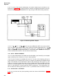
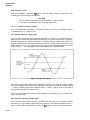
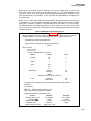
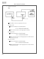
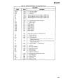
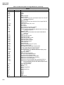
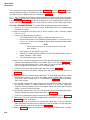
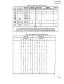
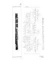
1
TM 11-6625-2941-14&P
TECHNICAL MANUAL
OPERATOR’S, ORGANIZATIONAL, DIRECT
SUPPORT, AND GENERAL SUPPORT
MAINTENANCE MANUAL, INCLUDING REPAIR
PARTS AND SPECIAL TOOLS LIST
FOR
COUNTER, ELECTRONIC, DIGITAL READOUT
AN/USM-459
(HEWLETT-PACKARD MODEL 5328A/E42)
(NSN 6625-01-061-8928) (EIC: KRV)
DISTRIBUTION STATEMENT B – Distribution authorized to U.S. Government Agencies only to
protect contractor proprietary rights. Recipient agrees not to reproduce, disclose, or transfer to
other documents all or any part of this document for any purpose without permission in writing
from Agilent Technologies, Inc. The U.S. Government has only limited rights to this data as
defined in DFARS 252.227-7013 (Nov. 1995). This determination was made 8 September 2005.
Other requests for this document shall be referred to Agilent Technologies, 3500 Deer Creek
Road, Palo Alto, CA 94304.
DESTRUCTION NOTICE – Destroy by any method that will prevent disclosure of contents or
reconstruction of the document.
HEADQUARTERS, DEPARTMENT OF THE ARMY
28 MARCH 1979
TM 11-6625-2941-14&P
C2
Headquarters
Department of the Army
Washington, D.C., 24 February2006
CHANGE
No.
2
OPERATOR’S, ORGANIZATIONAL, DIRECT SUPPORT,
AND GENERAL SUPPORT MAINTENANCE MANUAL, INCLUDING REPAIR PARTS
AND SPECIAL TOOLS LIST
FOR
COUNTER, ELECTRONIC, DIGITAL READOUT
AN/USM-459
(HEWLETT-PACKARD MODEL 5328A/E42)
(NSN 6625-01-061-8928) (EIC: KRV)
HAZARDOUS MATERIAL INFORMATION – This document has been reviewed for the presence
of solvents containing hazardous materials as defined by the EPCRA 302 and 313 lists by the
AMCOM G-4 (Logistics) Environmental Division. As of the base document through Change 1,
dated 25 August 2005, all references to solvents containing hazardous materials have been
removed from this document by substitution with non-hazardous or less hazardous materials
where possible.
OZONE DEPLETING CHEMICAL INFORMATION – This document has been reviewed for the
presence of Class I ozone depleting chemicals by the AMCOM G-4 (Logistics) Environmental
Division. As of the base document through Change 1, dated 25 August 2005, all references to
Class I ozone depleting chemicals have been removed from this document by substitution with
chemicals that do not cause atmospheric ozone depletion.
DISTRIBUTION STATEMENT B – Distribution authorized to U.S. Government Agencies only to
protect contractor proprietary rights. Recipient agrees not to reproduce, disclose, or transfer to
other documents all or any part of this document for any purpose without permission in writing
from Agilent Technologies, Inc. The U.S. Government has only limited rights to this data as
defined in DFARS 252.227-7013 (Nov. 1995). This determination was made 8 September 2005.
Other requests for this document shall be referred to Agilent Technologies, 3500 Deer Creek
Road, Palo Alto, CA 94304.
DESTRUCTION NOTICE – Destroy by any method that will prevent disclosure of contents or
reconstruction of the document.
TM 11-6625-2941-14&P, dated 28 March 1979, is changed as follows:
1. Remove old pages and insert new pages as indicated below. New or changed material is
indicated by a vertical bar in the outer margin of the page.
Remove Pages
A/(B blank)
i/(ii blank)
0-1/(0-2 blank)
A-1/(A-2 blank)
B-1 and B-2
B-3/(B-4 blank)
Insert Pages
A/(B blank)
i/(ii blank)
0-1/(0-2 blank)
A-1/(A-2 blank)
B-1 and B-2
B-3/(B-4 blank)
TM 11-6625-2941-14&P
C2
Remove Pages
Insert Pages
Cover
Cover
2. File this change sheet in front of the publication for reference purposes.
By Order of the Secretary of the Army:
PETER J. SCHOOMAKER
General, United States Army
Chief of Staff
Official:
SANDRA R. RILEY
Administrative Assistant to the
Secretary of the Army
0534904
Distribution:
To be distributed in accordance with the initial distribution number (IDN) 363372,
requirements for TM 11-6625-2941-14&P.
TM 11-6625-2941-14&P
C1
Headquarters
Department of the Army
CHANGE
Washington, D.C., 25 August 2005
No. 1
TECHNICAL MANUAL
OPERATOR’S, ORGANIZATIONAL, DIRECT SUPPORT
AND GENERAL SUPPORT MAINTENANCE MANUAL
INCLUDING REPAIR PARTS AND SPECIAL TOOLS LIST
FOR
COUNTER, ELECTRONIC, DIGITAL READOUT
AN/USM-459
(HEWLETT-PACKARD MODEL 5328A/E42)
(NSN 6625-01-061-8928) (EIC: N/A)
DISTRIBUTION STATEMENT B – Distribution authorized to U.S. Government Agencies only to
protect contractor proprietary rights. Recipient agrees not to reproduce, disclose, or transfer to
other documents all or any part of this document for any purpose without permission in writing
from Agilent Technologies, Inc. The U.S. Government has only limited rights to this data as
defined in DFARS 252.227-7013 (Nov. 1995). This determination was made 8 September 2005.
Other requests for this document shall be referred to Agilent Technologies, 3500 Deer Creek
Road, Palo Alto, CA 94304.
DESTRUCTION NOTICE – Destroy by any method that will prevent disclosure of contents or
reconstruction of the document.
TM 11-6625-2941-14&P, dated 28 March 1979, is changed as follows:
1. Remove old pages and insert new pages as indicated below. New or changed material is
indicated by a vertical bar in the outer margin of the page. Illustration changes are indicated
by a pointing hand. New or changed part numbers are indicated by an asterisk (*).
Completely revised sections or chapters are indicated by a vertical bar adjacent to the title
only.
2. This change implements Army Maintenance Transformation and changes the Maintenance
Allocation Chart (MAC) to support Field and Sustainment Maintenance.
Remove Pages
None
i/(ii blank)
D-1 thru D-5/(D-6 blank)
DA Forms 2028-2
COVER
Insert Pages
A/(B blank)
i/(ii blank)
D-1 thru D-6
DA Forms 2028
COVER
3. File this change sheet in front of the publication for reference purposes.
TM 11-6625-2941-14&P
C2
By Order of the Secretary of the Army:
PETER J. SCHOOMAKER
General, United States Army
Chief of Staff
Official:
SANDRA R. RILEY
Administrative Assistant to the
Secretary of the Army
0519208
Distribution:
To be distributed in accordance with the initial distribution number (IDN) 363372,
requirements for TM 11-6625-2941-14&P.
TM 11-6625-2941-14&P
INSERT LATEST CHANGED PAGES. DESTROY SUPERSEDED PAGES.
LIST OF EFFECTIVE PAGES
NOTE
ON CHANGED PAGES, THE PORTION OF THE TEXT AFFECTED BY THE LATEST CHANGE IS INDICATED BY A
VERTICAL LINE OR OTHER CHANGE SYMBOL IN THE OUTER MARGIN OF THE PAGE.
Date of issue for original and changed pages are:
Original 0
28 March 1979
Change 1
25 August 2005
Change 2
24 February 2006
Total number of pages in this publication is 222 consisting of the following:
Page
No.
* Change
No.
Cover................................................... 2
A ......................................................... 2
B blank................................................. 2
i............................................................ 2
ii blank ................................................. 2
iii through ix ......................................... 0
0 .......................................................... 0
0-1 ................................................... 2
0-2 blank.............................................. 2
1-1 through 1-4.................................... 0
2-1 through 2-3.................................... 0
2-4 blank.............................................. 0
3-1 through 3-19.................................. 0
3-20 blank............................................ 0
4-1 through 4-24.................................. 0
5-1 through 5-17.................................. 0
5-17A and 5-17B ................................ 0
5-19 through 5-46................................ 0
5-47 (Fig 5-10, SH. 1) ......................... 0
5-48 blank............................................ 0
5-49 (Fig 5-10, SH. 2) ......................... 0
5-50 blank............................................ 0
5-51 (Fig 5-10, SH. 3) ......................... 0
5-52 (Fig 5-11, SH. 1) ......................... 0
5-53 (Fig 5-11, SH. 2) ......................... 0
5-54 (Fig 5-12)..................................... 0
6-1 through 6-27.................................. 0
6-28 blank............................................ 0
7-1 through 7-3.................................... 0
7-4 blank.............................................. 0
8-1 through 8-9.................................... 0
8-10 blank............................................ 0
8-11 (Fig 8-6)....................................... 0
8-12 through 8-14................................ 0
8-15 (Fig 8-7, SH.1)............................. 0
Page
No.
*Change
No.
8-16 blank.......................................... 0
8-17 (Fig 8-7, SH. 2).......................... 0
8-18 (Fig 8-8)..................................... 0
8-19 (Fig 8-9)..................................... 0
8-20 ................................................... 0
8-21 (Fig 8-10)................................... 1
8-22 blank.......................................... 0
8-23 (Fig 8-11)................................... 0
8-24 ................................................... 0
8-25 (Fig 8-12)................................... 0
8-26 (Fig 8-13)................................... 0
8-27 (Fig 8-14)................................... 0
8-28 (Fig 8-15)................................... 0
8-29 (Fig 8-16)................................... 0
8-30 (Fig 8-17)................................... 0
8-31 (Fig 8-18)................................... 0
8-32 (Fig 8-19)................................... 0
8-33 (Fig 8-20)................................... 0
8-34 blank.......................................... 0
8-35 (Fig 8-21)................................... 0
8-36 ................................................... 0
8-37 (Fig 8-22)................................... 0
8-38 blank.......................................... 0
8-39 (Fig 8-23)................................... 0
8-40 ................................................... 0
8-41 (Fig 8-24)................................... 0
8-42 blank.......................................... 0
8-43 (Fig 25)...................................... 0
8-44 blank.......................................... 0
A-1 ..................................................... 2
A-2 blank ........................................... 2
B-1 through B-3 ................................. 2
B-4 blank ........................................... 2
D-1 through D-5................................. 0
D-6 blank ........................................... 0
* Zero in this column indicates an original page.
Change 2 A/(B blank)
Reproduced with Permission, courtesy of Agilent Technologies, Inc. Copyrighted by Agilent
Technologies, Inc., 2005. For Official U.S. Government Use Only.
TM 11-6625-2941-14&P
TECHNICAL MANUAL
NO. 11-6625-2941-14&P
HEADQUARTERS
DEPARTMENT OF THE ARMY
Washington, D.C., 28 March 1979
OPERATOR’S, ORGANIZATIONAL, DIRECT SUPPORT, AND GENERAL
SUPPORT MAINTENANCE MANUAL, INCLUDING REPAIR PARTS AND
SPECIAL TOOLS LIST
FOR
COUNTER, ELECTRONIC, DIGITAL READOUT
AN/USM-459
(HEWLETT-PACKARD MODEL 5328/E42)
(NSN 6625-01-061-8928) (EIC: KRV)
REPORTING ERRORS AND RECOMMENDING IMPROVEMENTS
You can help improve this manual. If you find any mistakes or if you know of a way to improve the procedures, please
let us know. Mail your letter or DA Form 2028 (Recommended Changes to Publications and Blank Forms) directly to:
Commander, U. S. Army Aviation and Missile Command, AMSAM-MMC-MA-NP, Redstone Arsenal, AL 35898-5000.
A reply will be furnished to you. You may also provide DA Form 2028 information to AMCOM via email, fax or the
World Wide Web. Our fax number is: DSN 788-6546 or Commercial 256-842-6546. Our email address is:
[email protected]. Instructions for sending an electronic 2028 may be found at the back of this manual
immediately preceding the hardcopy 2028. For the World Wide Web use: https://amcom2028.redstone.army.mil.
HAZARDOUS MATERIAL INFORMATION
This document has been reviewed for the presence of solvents containing hazardous materials as defined by
the EPCRA 302 and 313 lists by the AMCOM G-4 (Logistics) Environmental Division. As of the base
document through Change 1, dated 25 August 2005, all references to solvents containing hazardous materials
have been removed from this document by substitution with non-hazardous or less hazardous materials
where possible.
OZONE DEPLETING CHEMICAL INFORMATION
This document has been reviewed for the presence of Class I ozone depleting chemicals by the AMCOM G-4
(Logistics) Environmental Division. As of the base document through Change 1, dated 25 August 2005, all
references to Class I ozone depleting chemicals have been removed from this document by substitution with
chemicals that do not cause atmospheric ozone depletion.
DISTRIBUTION STATEMENT B – Distribution authorized to U.S. Government Agencies only to protect
contractor proprietary rights. Recipient agrees not to reproduce, disclose, or transfer to other documents all or
any part of this document for any purpose without permission in writing from Agilent Technologies, Inc. The
U.S. Government has only limited rights to this data as defined in DFARS 252.227-7013 (Nov. 1995). This
determination was made 8 September 2005. Other requests for this document shall be referred to Agilent
Technologies, 3500 Deer Creek Road, Palo Alto, CA 94304.
DESTRUCTION NOTICE – Destroy by any method that will prevent disclosure of contents or reconstruction of
the document.
TABLE OF CONTENTS
Section
Page
0
INTRODUCTION
0-1 Scope.......................................................................................................................... ................0-1
0-2 Consolidated Index of Army Publications and Blank Forms................................ ................0-1
0-3 Maintenance Forms, Records, and Reports............................................................................0-1
0-4 Reporting Equipment Improvement Recommendations (EIRs).............................. ..............0-1
0-5 Administrative Storage............................................................................................. ................0-1
0-6 Destruction of Army Electronics Materiel............................................................... ................0-1
Change 2 i/(ii blank)
Model 5328A
Table of Contents
TABLE OF CONTENTS
Page
Section
GENERAL INFORMATION . . . . . . . . . . . . . . . . . . . . . . . . . . . . . . . . . . . . . . . .
1-1.
Scope of Manual . . . . . . . . . . . . . . . . . . . . . . . . . . . . . . . . . . . . . . . . . .
1-4.
Description . . . . . . . . . . . . . . . . . . . . . . . . . . . . . . . . . . . . . . . . . . . . . . .
1-6.
Instrument Identification . . . . . . . . . . . . . . . . . . . . . . . . . . . . . . . . . . .
1-8.
Applications . . . . . . . . . . . . . . . . . . . . . . . . . . . . . . . . . . . . . . . . . . . . . .
1-16. Equipment Supplied and Accessories Available . . . . . . . . . . . . . .
1-18. Specifications . . . . . . . . . . . . . . . . . . . . . . . . . . . . . . . . . . . . . . . . . . . . .
1-1
1-1
1-1
1-1
1-2
1-2
1-2
II
INSTALLATION . . . . . . . . . . . . . . . . . . . . . . . . . . . . . . . . . . . . . . . . . . . . . . . . . .
Introduction . . . . . . . . . . . . . . . . . . . . . . . . . . . . . . . . . . . . . . . . . .
2-1.
2-3.
Unpacking and Inspection . . . . . . . . . . . . . . . . . . . . . . . . . . . . . . . . .
2-5.
Preparation for Use . . . . . . . . . . . . . . . . . . . . . . . . . . . . . . . . . . . . . . . .
2-6.
Power Requirements . . . . . . . . . . . . . . . . . . . . . . . . . . . . . . . . . . . .
Fuse Replacement and Installation . . . . . . . . . . . . . . . . . . . . . . . .
2-8.
Power Cables . . . . . . . . . . . . . . . . . . . . . . . . . . . . . . . . . . . . . . . . . . .
2-10.
2-13.
Operating Environment . . . . . . . . . . . . . . . . . . . . . . . . . . . . . . . . . .
Bench Operation . . . . . . . . . . . . . . . . . . . . . . . . . . . . . . . . . . . . . . . .
2-15.
Rack Mounting . . . . . . . . . . . . . . . . . . . . . . . . . . . . . . . . . . . . . . . . .
2-17.
2-19. Packaging for Shipment . . . . . . . . . . . . . . . . . . . . . . . . . . . . . . . . . . . .
2-20.
Original Packaging . . . . . . . . . . . . . . . . . . . . . . . . . . . . . . . . . . . . . .
2-24.
Other Packaging Methods . . . . . . . . . . . . . . . . . . . . . . . . . . . . . . .
2-26. Storage . . . . . . . . . . . . . . . . . . . . . . . . . . . . . . . . . . . . . . . . . . . . . .
2-1
2-1
2-1
2-1
2-1
2-1
2-1
2-2
2-2
2-2
2-2
2-2
2-3
2-3
Ill
OPERATION (OPERATORS INSTRUCTIONS) . . . . . . . . . . . . . . . . . . . . . .
3-1.
Introduction . . . . . . . . . . . . . . . . . . . . . . . . . . . . . . . . . . . . . . . . . . . . .
Frequency Measurements . . . . . . . . . . . . . . . . . . . . . . . . . . . . . . . . . .
3-3.
3-9.
Period Measurements . . . . . . . . . . . . . . . . . . . . . . . . . . . . . . . . . . . . .
3-13. Time Interval Measurements . . . . . . . . . . . . . . . . . . . . . . . . . . . . . . .
3-20. Ratio Measurements . . . . . . . . . . . . . . . . . . . . . . . . . . . . . . . . . . . .
3-23. Operating Controls . . . . . . . . . . . . . . . . . . . . . . . . . . . . . . . . . . . . . . . .
3-26. Function of Controls, Indicators, Inputs, and Outputs . . . . . . . .
Display . . . . . . . . . . . . . . . . . . . . . . . . . . . . . . . . . . . . . . . . . . . . . . . . .
3-27.
Power (Line) . . . . . . . . . . . . . . . . . . . . . . . . . . . . . . . . . . . . . . . . . . . .
3-29.
Reset . . . . . . . . . . . . . . . . . . . . . . . . . . . . . . . . . . . . . . . . . . . . . . . . . . .
3-31.
Sample Rate Control . . . . . . . . . . . . . . . . . . . . . . . . . . . . . . . . . . . .
3-33.
Arming . . . . . . . . . . . . . . . . . . . . . . . . . . . . . . . . . . . . . . . . . . . . . . . . .
3-35.
Frequency Resoluton, N Switch . . . . . . . . . . . . . . . . . . . . . . . .
3-37.
Input Channel Section . . . . . . . . . . . . . . . . . . . . . . . . . . . . . . . . . .
3-41.
A and B Channel Signal Conditioning . . . . . . . . . . . . . . . . . . .
3-44.
3-49.
Channel C Input . . . . . . . . . . . . . . . . . . . . . . . . . . . . . . . . . . . . . . . .
3-51.
“C’’ Channel Overload Indicator . . . . . . . . . . . . . . . . . . . . . . . .
Hysteresis Band of Trigger Levels . . . . . . . . . . . . . . . . . . . . . . . . .
3-53.
External Frequency Standard Input. . . . . . . . . . . . . . . . . . . . . . . .
3-57.
M a r k e r O u t p. .u. t. s. . . . . . . . . . . . . . . . . . . . . . . . . . . . . . . . . . . . .
3-59.
3-61.
Gate/Marker Out . . . . . . . . . . . . . . . . . . . . . . . . . . . . . . . . . . . . . . .
1 MHz and 10 MHz Frequency Standard Outputs . . . . . . . . . .
3-63.
Trigger Lights . . . . . . . . . . . . . . . . . . . . . . . . . . . . . . . . . . . . . . . . . . .
3-65.
3-68. Programming Operation . . . . . . . . . . . . . . . . . . . . . . . . . . . . . . . . . . .
3-71. Setting Add dress Switches . . . . . . . . . . . . . . . . . . . . . . . . . . . . . . . . . .
3-75. Measurement Output Format . . . . . . . . . . . . . . . . . . . . . . . . . . . . . .
3-77. Bus Commands . . . . . . . . . . . . . . . . . . . . . . . . . . . . . . . . . . . . . . . . . . .
3-79. Programming Examples . . . . . . . . . . . . . . . . . . . . . . . . . . . . . . . . . . . .
I
3-1
3-1
3-1
3-2
3-3
3-4
3-4
3-8
3-8
3-8
3-8
3-8
3-8
3-9
3-10
3-10
3-12
3-12
3-12
3-12
3-13
3-13
3-13
3-13
3-13
3-13
3-16
3-16
3-18
iii
Model 5328A
Table of Contents
TABLE OF CONTENTS (Continued)
Section
IV
Page
THEORY OF OPERATION . . . . . . . . . . . . . . . . . . . . . . . . . . . . . . . . . . . . . . . 4-1
4-1.
Introduction . . . . . . . . . . . . . . . . . . . . . . . . . . . . . . . . . . . . . . . . . . . . . 4-1
4-3.
Overall Description . . . . . . . . . . . . . . . . . . . . . . . . . . . . . . . . . . . . . . . 4-1
4-5.
Basic Counter Operation . . . . . . . . . . . . . . . . . . . . . . . . . . . . . . . . . 4-1
4-7.
Frequency . . . . . . . . . . . . . . . . . . . . . . . . . . . . . . . . . . . . . . . . . . . . . 4-1
4-15.
Period . . . . . . . . . . . . . . . . . . . . . . . . . . . . . . . . . . . . . . . . . . . . . . . . .
4-2
4-18.
Ratio . . . . . . . . . . . . . . . . . . . . . . . . . . . . . . . . . . . . . . . . . . . . . . . . . . 4-3
4-20.
Time Interval . . . . . . . . . . . . . . . . . . . . . . . . . . . . . . . . . . . . . . . . . . 4-3
4-22.
Time interval, Resolution, and Averaging Techniques . . . . . . .
4-3
Resolution . . . . . . . . . . . . . . . . . . . . . . . . . . . . . . . . . . . . . . . . . . . . . 4-4
4-24.
4-27.
Time Interval Averaging . . . . . . . . . . . . . . . . . . . . . . . . . . . . . . . . 4-4
4-34.
Sources of Measurement Error . . . . . . . . . . . . . . . . . . . . . . . . . . . . 4-5
±1 Count Ambiguity . . . . . . . . . . . . . . . . . . . . . . . . . . . . . . . . . . . .
4-36.
4-5
Time Base Error . . . . . . . . . . . . . . . . . . . . . . . . . . . . . . . . . . . . . . . . 4-6
4-41.
4-43.
Trigger Error . . . . . . . . . . . . . . . . . . . . . . . . . . . . . . . . . . . . . . . . . . .
4-6
4-48.
5328A Principles of Operation . . . . . . . . . . . . . . . . . . . . . . . . . . . . .
4-7
Main Counter Section . . . . . . . . . . . . . . . . . . . . . . . . . . . . . . . . . .
4-52.
4-7
4-57.
Input Section . . . . . . . . . . . . . . . . . . . . . . . . . . . . . . . . . . . . . . . . .
4-9
Hewlett-Packard Interface Bus (HP-lB) Section . . . . . . . . . . . . 4-9
4-60.
4-62.
Al Motherboard . . . . . . . . . . . . . . . . . . . . . . . . . . . . . . . . . . . . . . . . . 4-9
4-10
4-64.
Display Control . . . . . . . . . . . . . . . . . . . . . . . . . . . . . . . . . . . . . . . .
4-67.
State Control . . . . . . . . . . . . . . . . . . . . . . . . . . . . . . . . . . . . . . . . . . 4-10
4-69.
A3 Oscillator Support . . . . . . . . . . . . . . . . . . . . . . . . . . . . . . . . . . . . .
4-10
4-17.
A3 Oscillator Support . . . . . . . . . . . . . . . . . . . . . . . . . . . . . . . . . . . 4-10
4-73.
A3A1 Oscillator (HP 10544A) . . . . . . . . . . . . . . . . . . . . . . . . . . . .
4-10
4-75.
Decade Counting Assembly (DCA) . . . . . . . . . . . . . . . . . . . . . . . . .
4-10
4-79.
Time Base . . . . . . . . . . . . . . . . . . . . . . . . . . . . . . . . . . . . . . . . . . . . . . .
4-11
4-83.
A2 Power Supply . . . . . . . . . . . . . . . . . . . . . . . . . . . . . . . . . . . . . . . . .
4-11
+5V Supply . . . . . . . . . . . . . . . . . . . . . . . . . . . . . . . . . . . . . . . . . . . .
4-85.
4-11
4-89.
A4 Function Selector . . . . . . . . . . . . . . . . . . . . . . . . . . . . . . . . . . . . . 4-12
4-91.
High Speed Multiplexer, Main Gate, and 1st Decade . . . . . .
4-12
4-94.
Arming Multiplexer and Arming FF . . . . . . . . . . . . . . . . . . . .
4-12
4-96.
Time Base Multiplexer and Main Gate FF . . . . . . . . . . . . . . . . .
4-13
4-99.
An Example of Operation . . . . . . . . . . . . . . . . . . . . . . . . . . . . . . .
4-13
4-103. A16 Display Assembly . . . . . . . . . . . . . . . . . . . . . . . . . . . . . . . . . .
4-13
4-107. Remote Controllable (Programmable) Input Block
Diagram Description . . . . . . . . . . . . . . . . . . . . . . . . . . . . . . . .
4-14
4-115. Remote Controllable (Programmable) Input
Schematic Theory . . . . . . . . . . . . . . . . . . . . . . . . . . . . . . . . . . . .
4-16
4-117.
A19 Switch Control Board . . . . . . . . . . . . . . . . . . . . . . . . . . . . .
4-16
4-122.
A12 Amplifier Board . . . . . . . . . . . . . . . . . . . . . . . . . . . . . . . . . . . .
4-16
4-127.
A10 Synchronizer Board . . . . . . . . . . . . . . . . . . . . . . . . . . . . . . . .
4-17
4-147.
A11 DAC Board . . . . . . . . . . . . . . . . . . . . . . . . . . . . . . . . . . . . . . . .
4-19
4-156.
A8 Channel C lnput . . . . . . . . . . . . . . . . . . . . . . . . . . . . . . . . . . . .
4-20
4-162. HP interface Bus Theory . . . . . . . . . . . . . . . . . . . . . . . . . . . . . . . . . .
4-20
4-173. HP-lB A15 Interface Operation . . . . . . . . . . . . . . . . . . . . . . . . . . . .
4-21
4-178.
Overall Operation . . . . . . . . . . . . . . . . . . . . . . . . . . . . . . . . . . . . . . 4-22
Bus Command Mode . . . . . . . . . . . . . . . . . . . . . . . . . . . . . . . . . . . 4-22
4-181.
4-183.
Listen Mode . . . . . . . . . . . . . . . . . . . . . . . . . . . . . . . . . . . . . . . . . . .
4-22
4-185.
Talk Mode . . . . . . . . . . . . . . . . . . . . . . . . . . . . . . . . . . . . . . . . . . . . .
4-22
A15 Circuit Operation . . . . . . . . . . . . . . . . . . . . . . . . . . . . . . . . . .
4-187.
4-22
Model 5328A
Table of Contents
TABLE OF CONTENTS (Continued)
Page
Section
V
VI
Vll
MAINTENANCE . . . . . . . . . . . . . . . . . . . . . . . . . . . . . . . . . . . . . . . . . . . . . . . . .
Introduction . . . . . . . . . . . . . . . . . . . . . . . . . . . . . . . . . . . . . . . . . . . .
5-1.
Assembly Designations . . . . . . . . . . . . . . . . . . . . . . . . . . . . . . . . . .
5-3.
Test Equipment . . . . . . . . . . . . . . . . . . . . . . . . . . . . . . . . . . . . . . . . . . .
5-5.
Assembly Connection Identification . . . . . . . . . . . . . . . . . . . . . . . .
5-7.
Preventive Maintenance . . . . . . . . . . . . . . . . . . . . . . . . . . . . . . . . . . .
5-9.
5-11.
Inspection . . . . . . . . . . . . . . . . . . . . . . . . . . . . . . . . . . . . . . . . . . . . . .
Cleaning . . . . . . . . . . . . . . . . . . . . . . . . . . . . . . . . . . . . . . . . . . . . . . .
5-13.
Performance Test . . . . . . . . . . . . . . . . . . . . . . . . . . . . . . . . . . . . . . . .
5-15.
5-17. Repair . . . . . . . . . . . . . . . . . . . . . . . . . . . . . . . . . . . . . . . . . . . . . . . . . .
Printed Circuit Component Replacement . . . . . . . . . . . . . . . . . .
5-18.
Replacing Integrated Circuits . . . . . . . . . . . . . . . . . . . . . . . . . . . . .
5-20.
5-22. Adjustments . . . . . . . . . . . . . . . . . . . . . . . . . . . . . . . . . . . . . . . . . . . . .
Sensitivity Adjustments . . . . . . . . . . . . . . . . . . . . . . . . . . . . . . . . . .
5-25.
Adjustment of A3 Oscillator Support . . . . . . . . . . . . . . . . . . . . . .
5-26.
5-27. Troubleshooting . . . . . . . . . . . . . . . . . . . . . . . . . . . . . . . . . . . . . . . . .
5-29. Troubleshooting Aids . . . . . . . . . . . . . . . . . . . . . . . . . . . . . . . . . . . . . .
Extender Board (05328-62016) . . . . . . . . . . . . . . . . . . . . . . . . . . . . .
5-31.
lC Troubleshooting . . . . . . . . . . . . . . . . . . . . . . . . . . . . . . . . . . . .
5-33.
Function Signals . . . . . . . . . . . . . . . . . . . . . . . . . . . . . . . . . . . . . . .
5-35.
5-43. Troubleshooting Input Channels . . . . . . . . . . . . . . . . . . . . . . . . . . . .
Local Mode Troubleshooting . . . . . . . . . . . . . . . . . . . . . . . . . . . .
5-45.
5-54. Removal and Replacement Instructions . . . . . . . . . . . . . . . . . . . . . .
Instrument Cover Removal . . . . . . . . . . . . . . . . . . . . . . . . . . . . . . .
5-56.
Time Interval Module (Assemblies A10 and A19)
5-58.
Removal Replacement . . . . . . . . . . . . . . . . . . . . . . . . . . . . . . .
A16 Display Assembly Removal and Replacement . . . . . . . . . .
5-60.
5-1
5-1
5-1
5-1
5-1
5-2
5-3
5-3
5-3
5-3
5-3
5-3
5-19
5-19
5-24
5-24
5-24
5-24
5-26
5-26
5-41
5-41
5-45
5-45
REPLACEABLE PARTS . . . . . . . . . . . . . . . . . . . . . . . . . . . . . . . . . . . . . . . . . . . .
Introduction . . . . . . . . . . . . . . . . . . . . . . . . . . . . . . . . . . . . . . . . . . . . . .
6-1.
Ordering Information . . . . . . . . . . . . . . . . . . . . . . . . . . . . . . . . . . . . .
6-3.
HP Part Number Organization . . . . . . . . . . . . . . . . . . . . . . . . . . .
6-5.
6-7.
Component Parts and Materials . . . . . . . . . . . . . . . . . . . . . . . . . .
General Usage Parts . . . . . . . . . . . . . . . . . . . . . . . . . . . . . . . . . . . . .
6-10.
Specific Instrument Parts . . . . . . . . . . . . . . . . . . . . . . . . . . . . . . . . .
6-12.
6-14. Factory Selected Parts . . . . . . . . . . . . . . . . . . . . . . . . . . . . . . . . . . . . . .
6-16. Part Number to NSN Cross Reference Index . . . . . . . . . . . . . . . . .
MANUAL CHANGES . . . . . . . . . . . . . . . . . . . . . . . . . . . . . . . . . . . . . . . . . . . .
7-1.
Introduction . . . . . . . . . . . . . . . . . . . . . . . . . . . . . . . . . . . . . . . . . . . . . .
7-3. Manual Changes Sheet . . . . . . . . . . . . . . . . . . . . . . . . . . . . . . . . . . . .
6-1
6-1
6-1
6-3
6-3
6-4
6-4
6-4
6-4
7-1
7-1
7-1
5-45
5-45
8-1
SCHEMATIC DIAGRAMS . . . . . . . . . . . . . . . . . . . . . . . . . . . . . . . . . . . . . . . . .
8-1
Introduction . . . . . . . . . . . . . . . . . . . . . . . . . . . . . . . . . . . . . . . . . . . . . .
8-1.
8-1
Schematic Diagrams SymboIs and Reference Designators . . . . .
8-3.
8-1
Reference Designators . . . . . . . . . . . . . . . . . . . . . . . . . . . . . . . . . . .
8-5.
Signal Mnemonics . . . . . . . . . . . . . . . . . . . . . . . . . . . . . . . . . . . . . . . . . 8-1
8-7.
8-1
Identification Markings o Printed-Circuit Boards . . . . . . . . . . . . .
8-9.
8-2
8-14. Assembly Locations and Component Locators . . . . . . . . . . . . . . .
8-2
8-16. Factor Selected Components . . . . . . . . . . . . . . . . . . . . . . . . . . . . . . .
A-1
APPENDIX A. REFERENCES . . . . . . . . . . . . . . . . . . . . . . . . . . . . . . . ..
B-1
B. COMPONENTS OF END ITEM LIST . . . . . . . . . . . . . . . . . . . .
C. ADDITIONAL AUTHORIZATION LIST (not applicable)
D-1
D. MAINTENANCE ALLOCATION . . . . . . . . . . . . . . . . . . . .
E. EXPENDABLE SUPPLIES AND MATERIALS LIST (not applicable)
Vlll
v
Model 5328A
List of Tables
LIST OF TABLES
Page
Table
1-1.
1-2.
1-3.
Equipment Supplied . . . . . . . . . . . . . . . . . . . . . . . . . . . . . . . . . . . . . . . . . . . . . . 1-2
1-2
Accessories Available . . . . . . . . . . . . . . . . . . . . . . . . . . . . . . . . . . . . . . . . . . . . .
5328A Counter Specifications . . . . . . . . . . . . . . . . . . . . . . . . . . . . . . . . . . . . . . 1-3
3-1.
3-2.
3-3.
3-4.
3-5.
3-6.
Arming Status . . . . . . . . . . . . . . . . . . . . . . . . . . . . . . . . . . . . . . . . . . . . . . . . . . . 3-9
3-9
Frequency Resolution, N Switch Settings and Gate Times . . . . . . . . . . . .
Functions and Resolution Switch Settings . . . . . . . . . . . . . . . . . . . . . . . . . . . 3-9
Addressing . . . . . . . . . . . . . . . . . . . . . . . . . . . . . . . . . . . . . . . . . . . . . . . . . . . . . 3-14
Program Code Set . . . . . . . . . . . . . . . . . . . . . . . . . . . . . . . . . . . . . . . . . . . . . . . 3-15
3-17
American Standard Code for Information interchange (ASCII) . . . . . . .
4-1.
5328A input Circuit Program Code Set . . . . . . . . . . . . . . . . . . . . . . . . . . . .
5-1.
5-2.
5-3.
5-4.
5-5.
5-6.
5-7.
5-8.
5-9.
5-1o.
5-11.
5-12.
5-13.
5-14.
5-15.
5-16.
5-1
5328A Assembly identification . . . . . . . . . . . . . . . . . . . . . . . . . . . . . . . . . . . . .
5-2
Recommended Test Equipment . . . . . . . . . . . . . . . . . . . . . . . . . . . . . . . . . .
Preventive Maintenance . . . . . . . . . . . . . . . . . . . . . . . . . . . . . . . . . . . . . . . . . . . 5-2
Performance Test . . . . . . . . . . . . . . . . . . . . . . . . . . . . . . . . . . . . . . . . . . . . . . . . . 5-4
lC Troubleshooting, A1 Motherboard . . . . . . . . . . . . . . . . . . . . . . . . . . . . . 5-27
5328A Functional Signals . . . . . . . . . . . . . . . . . . . . . . . . . . . . . . . . . . . . . . . . . 5-30
5-33
Program Listing . . . . . . . . . . . . . . . . . . . . . . . . . . . . . . . . . . . . . . . . . . . . . . .
Program Description . . . . . . . . . . . . . . . . . . . . . . . . . . . . . . . . . . . . . . . . . . . . . 5-36
5328A A15 Qualifiers and Signal Mnemonics . . . . . . . . . . . . . . . . . . . . . . . 5-39
A12 Relay Operation . . . . . . . . . . . . . . . . . . . . . . . . . . . . . . . . . . . . . . . . . . . . . 5-41
Relay Control Logic . . . . . . . . . . . . . . . . . . . . . . . . . . . . . . . . . . . . . . . . . . . . . . 5-41
Program interface Operation . . . . . . . . . . . . . . . . . . . . . . . . . . . . . . . . . . . . . 5-43
ROM (A10U7) Input/Output Mode . . . . . . . . . . . . . . . . . . . . . . . . . . . . . . . 5-43
5-44
A11 DAC Logic Levels . . . . . . . . . . . . . . . . . . . . . . . . . . . . . . . . . . . . . . . . . .
A11 DAC Signals . . . . . . . . . . . . . . . . . . . . . . . . . . . . . . . . . . . . . . . . . . . . . . . . 5-44
A11 DAC Troubleshooting . . . . . . . . . . . . . . . . . . . . . . . . . . . . . . . . . . . . . . . . 5-44
6-1.
6-2.
6-3.
Replaceable Parts . . . . . . . . . . . . . . . . . . . . . . . . . . . . . . . . . . . . . . . . . . . . . . . 6-5
Manufacturers Code List . . . . . . . . . . . . . . . . . . . . . . . . . . . . . . . . . . . . . . . . . 6-24
Part Number-NSN Cross Reference Index . . . . . . . . . . . . . . 6-25
4-15
LIST OF FIGURES
Figure
Page
1-1.
Model 5328A 500 MHz Universal Frequency Counter . . . . . . . . . . . . . . . 1-0
3-1.
3-2.
3-3.
3-4.
3-5.
3-6.
3-7.
3-8.
3-9.
3-10.
3-11.
3-13.
Measuring Linearity . . . . . . . . . . . . . . . . . . . . . . . . . . . . . . . . . . . . . . . . . . . . . . . 3-2
Tone Burst Measurements . . . . . . . . . . . . . . . . . . . . . . . . . . . . . . . . . . . . . . . . . 3-2
Deadtime . . . . . . . . . . . . . . . . . . . . . . . . . . . . . . . . . . . . . . . . . . . . . . . . . . . . . . . .
3-3
Multiple STOP Pulses . . . . . . . . . . . . . . . . . . . . . . . . . . . . . . . . . . . . . . . . . .
Monitoring Marker Outputs . . . . . . . . . . . . . . . . . . . . . . . . . . . . . . . . . . . . . . . 3-4
3-5
5328A Front Panel Operation Summary . . . . . . . . . . . . . . . . . . . . . . . . . . . .
5328A Rear Panel Controls and Connectors . . . . . . . . . . . . . . . . . . . . . . . . . 3-7
3-10
Programmable Input Switch Configuration for COM A . . . . . . . . . . . . .
3-11
Slope Switch Settings . . . . . . . . . . . . . . . . . . . . . . . . . . . . . . . . . . . . . .
3-11
.
.
.
.
.
.
.
.
.
.
.
.
.
.
.
.
.
.
.
.
.
.
.
.
.
.
.
.
.
.
.
.
.
.
.
Level Control Settings . . . . . . . . .
Hysteresis Band . . . . . . . . . . . . . . . . . . . . . . . . . . . . . . . . . . . . . . . . . . . . . . . 3-12
5328A Measurement Cycle . . . . . . . . . . . . . . . . . . . . . . . . . . . . . . . . . . . . . . 3-18
Model 5328A
List of Figures
LIST OF FIGURES
4-1.
4-2.
4-3.
4-4.
4-5.
4-6.
4-7.
4-8.
4-9.
4-10.
Basic Elements of the Frequency Counter . . . . . . . . . . . . . . . . . . . . . . . . . . .
Measuring Period . . . . . . . . . . . . . . . . . . . . . . . . . . . . . . . . . . . . . . . . . . . . . . . . .
Basic Elements of a Time interval Counter . . . . . . . . . . . . . . . . . . . . . . . . . .
Clock Pulses . . . . . . . . . . . . . . . . . . . . . . . . . . . . . . . . . . . . . . . . . . . . . . . . . . . . .
Synchronizer Operation with Time Interval Averaging . . . . . . . . . . . . . . .
±1 Count Ambiguity . . . . . . . . . . . . . . . . . . . . . . . . . . . . . . . . . . . . . . . . . . . . . .
Trigger Error . . . . . . . . . . . . . . . . . . . . . . . . . . . . . . . . . . . . . . . . . . . . . . . . . . . . .
Block Diagram . . . . . . . . . . . . . . . . . . . . . . . . . . . . . . . . . . . . . . . . . . . . . . . . . . .
Remote Controllable (Programmable) Input Block Diagram . . . . . . . . .
ASM Oscillator Timing Diagram . . . . . . . . . . . . . . . . . . . . . . . . . . . . . . . . . . .
4-1
4-2
4-3
4-3
4-5
4-5
4-7
4-8
4-14
4-24
5-1.
5-2.
5-3.
5-4.
5-5.
5-6.
5-7.
5-8.
5-8.
5-9.
5-10.
5-10.
5-10.
5-11.
5-11.
5-12.
10 MHz Oscillator Frequency Check . . . . . . . . . . . . . . . . . . . . . . . . . . . . . .
DAC Adjustment Equipment Connectors . . . . . . . . . . . . . . . . . . . . . . . . . .
DAC Adjustment Oscilloscope Readout and Adjustment Locations . .
Hookup for A3 Oscillator Support Adjustment . . . . . . . . . . . . . . . . . . . . .
A3 Jitter Adjustment . . . . . . . . . . . . . . . . . . . . . . . . . . . . . . . . . . . . . . . . . . . . .
System Configuration . . . . . . . . . . . . . . . . . . . . . . . . . . . . . . . . . . . . . . . . . . . .
Sample Printout . . . . . . . . . . . . . . . . . . . . . . . . . . . . . . . . . . . . . . . . . . . . . . . . .
Hookup for
Hookup for Test Described in Table 5-8B and C . . . . . . . . . . . . . . . . . . . .
Triangular Pulse Observed in Steps 5 and 7, Table 5-8B . . . . . . . . . . . . .
Assembly Flowchart (Sheet 1 of 3) . . . . . . . . . . . . . . . . . . . . . . . . . . . . . . . . .
Assembly Flowchart (Sheet 2 of 3) . . . . . . . . . . . . . . . . . . . . . . . . . . . . . . . . .
Assembly Flowchart (Sheet 3 of 3) . . . . . . . . . . . . . . . . . . . . . . . . . . . . . . . . .
Local Troubleshooting Flowchart (Sheet 1 of 2) . . . . . . . . . . . . . . . . . . . . .
Local Troubleshooting Flowchart (Sheet 2 of 2) . . . . . . . . . . . . . . . . . . . . .
Address Switch Troubleshooting Flowchart . . . . . . . . . . . . . . . . . . . . . . . .
5-19
5-22
5-23
5-24
5-25
5-31
5-32
8-1.
8-2.
8-3.
8-4.
8-5.
8-6.
8-7.
8-7.
8-8.
8-9.
8-10.
8-11.
8-12.
8-13.
8-14.
8-15.
8-16.
8-17.
8-18.
8-19.
8-20.
8-21.
8-22.
8-23.
8-24.
8-25.
Schematic Diagram Notes . . . . . . . . . . . . . . . . . . . . . . . . . . . . . . . . . . . . . . . . .
5328A Front View . . . . . . . . . . . . . . . . . . . . . . . . . . . . . . . . . . . . . . . . . . . . . . . . .
5328A Rear View . . . . . . . . . . . . . . . . . . . . . . . . . . . . . . . . . . . . . . . . . . . . . . . . .
5328A Top View . . . . . . . . . . . . . . . . . . . . . . . . . . . . . . . . . . . . . . . . . . . . . . . . . .
5328A Bottom View . . . . . . . . . . . . . . . . . . . . . . . . . . . . . . . . . . . . . . . . . . . . . . .
A1 Motherboard . . . . . . . . . . . . . . . . . . . . . . . . . . . . . . . . . . . . . . . . . . . . . . . .
A1 Motherboard Schematic and Components (Sheet 1 of 2) . . . . . . . . .
A1 Motherboard Schematic and Components (Sheet 2 of 2) . . . . . . . . .
A2 Power Supply Block Diagram . . . . . . . . . . . . . . . . . . . . . . . . . . . . . . . . . .
A2 Power Supply Schematic and Components . . . . . . . . . . . . . . . . . . . . . .
A3/A3A1 Oscillator Support Schematic and Components . . . . . . . . . . . . .
A4 Function Selector Block Diagram . . . . . . . . . . . . . . . . . . . . . . . . . . . . . .
A4 Function Selector Schematic and Components . . . . . . . . . . . . . . . . . .
A8 Channel “C” Block Diagram . . . . . . . . . . . . . . . . . . . . . . . . . . . . . . . . . . .
A8 Channel “C” Schematic and Components . . . . . . . . . . . . . . . . . . . . . .
A10 Synchronizer Block Diagram . . . . . . . . . . . . . . . . . . . . . . . . . . . . . . . . . .
A10 Synchronizer Schematic and Components . . . . . . . . . . . . . . . . . . . . .
A11 Digital-to-Analog Converter Block Diagram . . . . . . . . . . . . . . . . . . . .
A11 Digital-to-Analog Converter Schematic and Components . . . . . . .
A12 “A-B” Channel Block Diagram . . . . . . . . . . . . . . . . . . . . . . . . . . . . . . . .
A12 “A-B” Channel Schematic and Components . . . . . . . . . . . . . . . . . . .
A15 HP-IB Interface Block Diagram . . . . . . . . . . . . . . . . . . . . . . . . . . . . . .
A15 HP-IB Interface Schematic and Components . . . . . . . . . . . . . . . . . . .
A16 Display Block Diagram . . . . . . . . . . . . . . . . . . . . . . . . . . . . . . . . . . . . . . .
A16 Display Schematic and Components . . . . . . . . . . . . . . . . . . . . . . . . . .
A19 Switch/Attenuator Schematic and Components . . . . . . . . . . . . . . . .
5-36
5-38
5-47
5-49
5-51
5-52
5-53
5-54
8-3
8-7
8-7
8-8
8-9
8-11
8-17
8-19
8-18
8-19
8-21
8-23
8-25
8-26
8-27
8-28
8-29
8-30
8-31
8-32
8-33
8-35
8-37
8-39
8-41
8-43
vii
Model 5328A
Safety Considerations
SAFETY
CONSIDERATIONS
GENERAL
This is a Safety Class I instrument. This instrument has been designed and tested according to
IEC Publication 348, “Safety Requirements for Electronic Measuring Apparatus.”
OPERATION
BEFORE APPLYING POWER verify that the power transformer primary is matched to the
available line voltage and the correct fuse is installed (see Section II). Make sure that only
fuses with the required rated current and of the specified type (normal blow, time delay, etc.) are
used for replacement. The use of repaired fuses and the short-circuiting of fuseholders must
be avoided.
SERVICE
Although this instrument has been designed in accordance with international safety standards,
this manual contains information, cautions, and warnings which must be followed to ensure
safe operation and to retain the instrument in safe condition. Service and adjustments should
be performed only by qualified service personnel.
Any adjustment, maintenance, and repair of the opened instrument under voltage should be
avoided as much as possible and, when inevitable, should be carried out only by a skilled person
who is aware of the hazard involved.
Capacitors inside the instrument may still be charged even if the instrument has been disconnected from its source of supply.
Whenever it is likely that the protection has been impaired, the instrument must be made inoperative and be secured against any unintended operation.
viii
Model 5328A
Safety Considerations
WARNING
IF THIS INSTRUMENT IS TO BE ENERGIZED VIA AN AUTOTRANSFORMER (FOR VOLTAGE REDUCTION] MAKE SURE THE COMMON
TERMINAL IS CONNECTED TO THE EARTHED POLE OF THE POWER
SOURCE.
WARNING
BEFORE SWITCHING ON THE INSTRUMENT, THE PROTECTIVE EARTH
TERMINALS OF THE INSTRUMENT MUST BE CONNECTED TO THE
PROTECTIVE CONDUCTOR OF THE (MAINS) POWER CORD. THE
MAINS PLUG SHALL ONLY BE INSERTED IN A SOCKET OUTLET PROVIDED WITH A PROTECTIVE EARTH CONTACT. THE PROTECTIVE
ACTION MUST NOT BE NEGATED BY THE USE OF AN EXTENSION
CORD (POWER CABLE) WITHOUT A PROTECTIVE CONDUCTOR
(GROUNDING).
WARNING
THE SERVICE INFORMATION FOUND IN THIS MANUAL IS OFTEN
USED WITH POWER SUPPLIED AND PROTECTIVE COVERS REMOVED
FROM THE INSTRUMENT. ENERGY AVAILABLE AT MANY POINTS
MAY, IF CONTACTED, RESULT IN PERSONAL INJURY.
C A U T I O N
BEFORE SWITCHING ON THIS INSTRUMENT:
1.
MAKE SURE THE INSTRUMENT IS SET TO THE VOLTAGE OF
THE POWER SOURCE.
2.
ENSURE THAT ALL DEVICES CONNECTED TO THIS INSTRUMENT ARE CONNECTED TO THE PROTECTIVE (EARTH) GROUND.
3.
ENSURE THAT THE LINE POWER (MAINS) PLUG IS CONNECTED TO A THREE-CONDUCTOR LINE POWER OUTLET THAT HAS
A PROTECTIVE (EARTH) GROUND. (GROUNDING ONE CONDUCTOR OF A TWO-CONDUCTOR OUTLET IS NOT SUFFICIENT.)
4.
MAKE SURE THAT ONLY FUSES WITH THE REQUIRED RATED
CURRENT AND OF THE SPECIFIED TYPE (NORMAL BLOW,
TIME DELAY, ETC.) ARE USED FOR REPLACEMENT. THE USE
OF REPAIRED FUSES AND THE SHORT-CIRCUITING OF FUSE
HOLDERS MUST BE AVOIDED.
ix
Model 5328A
General Information
Figure 1-1. Model 5328A 500 MHz Universal Frequency Counter
0
TM 11-6625-2941-14&P
SECTION 0
INSTRUCTIONS
0-1. SCOPE.
This manual describes Counter, Electronic, Digital Readout AN/USM-459 and provides
instructions for operation and maintenance. Throughout this manual, the AN/USM-459 is
referred to as Hewlett-Packard Model 5328A Counter.
0-2. CONSOLIDATED INDEX OF ARMY PUBLICATIONS AND BLANK FORMS.
Refer to the latest issue of DA PAM 25-30 to determine whether there are new additions,
changes, or additional publications pertaining to this equipment.
0-3. MAINTENANCE FORMS, RECORDS, AND REPORTS.
a. Report of Maintenance and Unsatisfactory Equipment. Department of the Army
forms and procedures used for equipment maintenance will be those prescribed by DA PAM
750-8.
b. Report of Packaging and Handling Deficiencies. Fill out and forward SF 364 Report
of Discrepancy (ROD) as prescribed in AR 735-11-2/DLAR 4140.55/NAVMATINST
4355.73B/AFR 400-54/MCO 4430.3H.
Fill out and forward
c. Discrepancy in Shipment Report (DISREP) (SF 361).
Discrepancy in Shipment Report (DISREP) (SF 361) as prescribed in AR 55-38/NAVSUPINST
4610.33C/AFR 75-18/MCO P4610.19D/DLAR 4500.15.
0-4. REPORTING EQUIPMENT IMPROVEMENT RECOMMENDATIONS (EIRs).
If your Test Set needs improvement, let us know. Send us an EIR. You the user are the
only one who can tell us what you don’t like about your equipment. Let us know why you don’t
like the design or performance. Put it on an SF 368 (Product Quality Deficiency Report). Mail it
to us at: Commander, U.S. Army Aviation and Missile Command, AMSAM-MMC-MA-NM,
Redstone Arsenal, AL. 35898-5000. We will send you a reply.
0-5. ADMINISTRATIVE STORAGE.
Administrative storage of equipment issued to and used by Army activities shall be in
accordance with paragraph 2-26.
0-6. DESTRUCTION OF ARMY ELECTRONICS MATERIEL.
Destruction of Army Electronics Materiel to Prevent Enemy Use shall be in accordance
with TM 750-244-2.
Change 2 0-1/(0-2 blank)
Model 5320A
General Information
SECTION I
GENERAL
INFORMATION
1-1. SCOPE OF MANUAL
1-2. This manual provides operating and service information for the Hewlett-Packard Model
5328A/H42 500 MHz Universal Frequency Counter. (In this manual its name will be abbreviated
to “5328A” or “counter”.) A separate operators booklet contains condensed operator instructions.
1-3. This manual is divided into eight sections as listed and described below:
Section I
GENERAL INFORMATION — Describes the counter, lists specifications, lists
items supplied, lists items required, but not supplied, describes applications,
and lists recommended maintenance and test equipment.
Section II
INSTALLATION — Provides instructions for unpacking, inspection, preparation for use, preparation for reshipment, and preparation for storage.
Section Ill
OPERATION — Provides operator instructions including frequency, measurement of input signal: time period, time period average, time interval, time
interval average, and ratio between frequencies of two input signals.
Section IV
THEORY OF OPERATION — Covers a. description of the general operating
principles of the counter with reference to block and schematic diagrams
of each assembly.
Section V
MAINTENANCE — Contains maintenance and service information, including
a list of assemblies, recommended test equipment, performance checks, and
adjustment. Troubleshooting procedures and flowcharts are included in this
section.
Section VI
REPLACEABLE PARTS — Provides a complete list of replaceable parts and
parts ordering information.
Section VII
MANUAL CHANGES — Contains information on manual changes.
Section Vlll
CIRCUIT DIAGRAMS — Contains schematic diagrams and component locating illustrations.
1-4.
DESCRIPTION
1-5. The 5328A counter can be used to measure frequency, period, period average, time
interval, time interval average, and ratio. The 5328A provides a 9-digit LED display, display
storage, and leading zero blanking. Decimal point and unit readouts are displayed automatically.
Two independent selectable input channels are provided for time interval measurements. Each
input channel has an attenuator, trigger slope selector, level control, ac or dc coupling, and an
oscilloscope marker output. Rear panel connectors provide a gate output, one- and 10-megahertz output, and an input for an external frequency standard. An ARM switch on the rear panel
allows arming by the signal being measured (switch OFF) or by another input signal (switch ON).
1-6. INSTRUMENT IDENTIFICATION
1-7. Hewlett-Packard instruments have a 2-section, 10-character serial number (0000A00000),
which is located on the rear panel. The 4-digit serial prefix identifies instrument changes. If
the serial prefix of your instrument differs from that listed on the title page of this manual, there
are differences between this manual and your instrument. Instruments having higher serial
prefixes are covered with a “Manual Changes” sheet included with this manual.
1-1
Model 5328A
General Information
1-8.
APPLICATIONS
1-9. Specific applications information is provided in Section III of this manual. The general
application features of the 5328A are described in the following paragraphs.
1-10. The high sensitivity, frequency range, and signal conditioning controls (see Table 7-3)
make the 5328A suited for a wide range of applications.
1-11. The rear panel controlled “ARM” feature of the 5328A is useful in applications such as
burst frequency measurements, and pulse ampltiude measurements.
1-12. The 5328A single-shot resolution of 100 ns meets the requirements for applications
such as mechanical and electromechanical device (relays) timing, time of flight measurements
(ballistics), sonar ranging, radio ranging, and navigation.
1-13. Using time interval averaging, time intervals as short as 100 picosecond, with resolution
to 10 picosecond may be measured. Applications include coaxial cable length measurements,
phase measurements, logic timing measurements, and integrated circuit propagation delay
measurement.
1-14. Full bandwidth, sensitivity, and signal conditioning of the Channel A, B, and C input
amplifiers is provided for ratio and totalizing measurements.
1-15. The 5328A HP-IB Interface is able to output measurement data and be controlled (fully
programmed) via the Hewlett-Packard Interface Bus (HP-16). The 5328A may be interfaced
to HP-IB compatible instruments, calculators, or computers by interconnecting with an HP-IB
cable.
1-16. EQUIPMENT SUPPLIED AND ACCESSORIES AVAILABLE
1-17. Table 7-7 lists equipment supplied with the 5328A and Table 7-2 lists accessories available, The Service Kits listed in Table 1-2 are described in Section III.
Table 1-1. Equipment Supplied
DESCRIPTION
HP PART NUMBER
1
8120-1348
05328-62016
Detachable Power Cord 231 cm (7 /2 ft.) long
Extender Board, 18 pin
Table 1-2. Accessories Available
DESCRIPTION
HP Interface Bus Interconnect Cable
HP PART NUMBER
10631A, 914 mm (3 ft. long)
10631B, 1828 mm (6 ft. long)
10631C, 3656 mm (12 ft. long)
10631D, 0.5 m (11/2 ft. long)
Front Handle Kit
Rack Flange Kit (for instruments without handles)
Rack and Handle Kit (installation instructions included
with above kits)
Service Kit:
Function Selector and ROM Kit
1-18. SPECIFICATIONS
1-19. Table 1-3 lists detailed specifications for the 5328AF/096.
1-2
5061-0088
5061-0076
5061-0082
05328-82004
Model 5328A
General Information
Table 1-3. 5328A Counter Specifications
GENERAL
Power Requirements: 115 or 230 volts 60 or
400 Hz ac.
Display: Nine-digit LED.
Sample Rate: Variable from less than 2 milliseconds to HOLD.
Arming: Rear panel ARM (ON-OFF) switch.
Refer to operation for details.
Blanking: Unwanted zeros to left of mostsignificant-digit are suppressed.
Hold: HOLDS count between samples.
Trigger Light: Indicates input is above trigger
level.
PROGRAMMABLE OPERATION
(CHANNELS A AND B)
Includes independent selection of coupling,
trigger slope, trigger level, and attenuator for
each channel. Separate/Common A switch is
programmable. Also, an invert feature switches
Channels A and B; useful in all functions except
Ratio B/A.
Trigger level is programmable in 10 mV steps
in X1; 100 mV in X10; IV in X100.
Trigger level accuracy under remote control:
X1: ±35 mV
X10: ±350 mV +2% of trigger level
X100: ±3.5V +2% of trigger level
Input Characteristics
Sensitivity: 15 mV rms, 0—35 MHz (decoupled
20 Hz—35 MHz (ac coupled)
50 mV rms, 35 MHz—100 MHz
Minimum pulse width 5 ns, 140 mV p-p.
Coupling: ac or dc switch selectable.
Impedance: 1 MO II <70 pF.
Trigger Level: Variable over ±2.5 volts times
attenuator setting with 0 volt preset position.
Trigger Slope: Independent selection of + or
- slope.
Attenuators: X1, X10, X100.
Dynamic Range: 25 mV to 1V rms times
attenuator setting, 0—35 MHz; 50 mV rms
times attenuator setting, 35 MHz to 100 MHz
Maximum Input:
dc coupled,7 X1: 250V rms, dc — SO kHz
1.25 x 10 V rms/freq., 50 kHz—2.5 MHz
5V rms, 2.5 MHz—100 MHz.
dc coupled, X10 and X100: 250V rms, dc 5
MHz 1.25 x 10⁹V rms/freq., 5—100 MHz
ac coupled: 200V (peak ac + dc),
0-20 Hz; same as dc coupled above 20 Hz.
Channel Input: Separate or Common A.
Marker Outputs: A and B channel Schmidt
trigger outputs available on front panel;
0 to 300 mV levels into 50Q; <20 ns delay.
Period Measurements
Period A
Range: 0—10 MHz
Resolution: 10 ns to 0.1s in decade steps.
Accuracy: ±1 count ± time base error
±trigger error*
Display: ns, ps, ms.
Period Average A
Range: 0—10 MHz
Resolution: 100 ns—.01 ps in decade steps.
Accuracy: ±1 count displayed ± time base
error
trigger error*
±
no. of periods averaged
Display: Ps, ns
Time Interval Measurements
Time Interval A to B 8
Range: 100 ns to 10 seconds
Resolution: 100 ns to 1-second in decade
steps.
Accuracy: ±1 count ± time base error
± trigger error*
Display: ps, ms, s.
Time Interval Average A to B
Range: 0.1 ns to 10 seconds
Resolution:
Accuracy:
Minimum Dead Time: 150 ns from one
STOP to next START
Maximum Repetition Rate: 10 MHz.
Display: Ps, ns.
Ratio Measurement
Ratio B/A, or C/A
Range: A: 0—10 MHz
Range: B: 0—100 MHz
Range: C: 30—500 MHz
Resolution: 1 part in ~ x N
Accuracy: ±1 count of B or C ± trigger
error* of A times frequency of B or C (N>1)
For N=1, add 12 ns times frequency of
B or C.
* Trigger error is <0.3% of one period for sine waves
of 40 dB S/N or better and amplitude equal to
sensitivity of counter. For any wave shape, trigger
error is than then:
Frequency Measurements
Frequency A
Range: 0—100 MHz direct count.
Resolution: 1 MHz to 0.1 Hz in decade steps.
Accuracy: ±1 count ± time base error.
Display: Hz, kHz, MHz.
1-3
Model 5328A
General Information
Table 7-3. 5328A Counter Specifications (Continued)
CHANNEL C
Input Characteristics
Range: 30 MHz to 500 MHz direct count
Sensitivity: 15 mV rms, 30 MHz—500 MHz
Trigger level: 0 volts
Impedance: 50fl nominal
Maximum Input: 5 volts rms
Input protection: Input BNC fused; accessible
from front panel. protected to 200 volts peak.
overload Indicator: flashing indicator warns
of potential overload conditions.
Resolution: 1 MHz to 0.1 Hz in decade steps
Accuracy: ±1 count ± time base error
Display: Hz, kHz, MHz
1-4
TIME BASE
Outputs: 1 MHz and 10 MHz available at rear
panel BNC in standby and operate modes
Output level: 1 volts rms into 50f)
External Input: Operates from 1, 2.5, 5, and 10
MHz inputs at 1V rms.
Input impedance 1 K~l<30 pF
Counter automatically switches to
external mode when external input is
present.
Oscillator Aging Rate: <5x10 10/day after
24-hour warmup. Oscillator oven is
energized when power cable is connected
to line voltage.
Model 5328A
Installation
SECTION
II
INSTALLATION
2-1.
INTRODUCTION
2-2. This section provides instructions for unpacking, inspection, preparation for use, shipment, and storage.
2-3. UNPACKING AND INSPECTION
2-4. If the shipping carton is damaged, inspect the counter for visible damage (scratches,
dents, etc.). If the counter is damaged, notify the carrier and the nearest Hewlett-Packard
Sales and Service Office immediately (offices are listed at the back of this manual). Keep the shipping carton and packing material for the carrier’s inspection.
2-5. PREPARATION FOR USE
CAUTION
Before connecting this instrument to an ac power line, be sure that
the 115—230-volt line selector switch on the rear panel is set to the
proper position and proper line fuse is installed (see below).
2-6. Power Requirements
2-7. This instrument can be operated on single phase 115 or 230 (-10%. +5%) volts ac. Power
required is approximately 100 VA maximum. To avoid instrument damage, the rear panel line
selector switch must be set to the correct position and the correct fuse (as labeled on the rear
panel) must be installed. See Section III for rear panel features photograph. When shipped, the
switch is set to 115-volt ac operation.
2-8. Fuse Replacement and Installation
2-9. Two fuses are supplied with the instrument. The instrument is shipped with a 2.0 ampere
fuse installed for 115- volt operation. To change the instrument for 230-volt operation disconnect the ac power cable, set the line selector switch and install the 1.0 ampere fuse.
2-10. Power Cables
WARNING
TO PROTECT OPERATING AND SERVICING PERSONNEL, THIS
INSTRUMENT IS EQUIPPED WITH A THREE-PIN POWER RECEPTACLE. THE CENTER PIN OF THE RECEPTACLE CONNECTS THE
INSTRUMENT CHASSIS AND PANELS TO EARTH GROUND WHEN
USED WITH A PROPERLY WIRED THREE CONDUCTOR OUTLET
AND POWER CABLE. IMPROPERLY GROUNDED EQUIPMENT CAN
RESULT IN HAZARDOUS POTENTIALS BETWEEN EQUIPMENTS.
2-1
Model 5328A
Installation
2-11. To accommodate the different power receptacles used throughout the world, this instrument is supplied with one of the power cables shown in Figure 2-7. The cable supplied for use
in the United States meets the specifications established by the International Electrotechnical
Commission (lEC). The male connector of this cable is a NEMA type and the female connector
is a C.E.E. type.
2-12. Connect the power cable to a power source receptacle that has a grounded third conductor. If the line power receptacle is a two-pin type instead of a three-pin receptacle, use a
two- to three-pin adapter (HP Part No. 1251-0048 for USA applications) and connect the green
lead on the adapter to earth ground. See warning above. If counter is to be operated with 230V ac
line power, an Underwriters Laboratories listed connector should be used to connect power.
2-13. Operating Environment
2-14. Maximum and minimum allowable operating temperatures are listed in Table 1-3. If
these limits are exceeded at the installation site, auxiliary cooling or heating should be used to
keep the environment within limits. A l-inch space above the counter should be clear to allow
cooling air circulation. The cooling fan exhaust port at rear is to be kept clear.
2-15. Bench Operation
2-16. The instrument cabinet has plastic feet and the large tilt carrying handle will fold under
for convenient bench operation. The tilt handle permits inclining the instrument for ease in
using front-panel controls and indicators.
NOTE
The tilt carrying handle may be secured in any position by tightening
the knurled side screws.
2-17. Rack Mounting
2-18. The counter is ready for bench operation as shipped from the factory. To mount the
counter in a rack, it is necessary to order and install the rack flange kit listed in Table 7-2.
CAUTION
Ambient temperature in rack during operation should not exceed 112°F
(50°C). Be sure instrument position in rack permits adequate air circulation and that nearby equipment does not discharge hot air directly on
the instrument.
2-19. PACKAGING FOR RESHIPMENT
2-20. Original Packaging
2-21. The same containers and materials used in factory packaging can be obtained through
the Hewlett-Packard Sales and Service Offices listed at the rear of this manual.
2-22. If the counter is being returned to Hewlett-Packard for service, attach a tag indicating
the type of service required, return address, model number, and full serial number. Mark the
container FRAGILE to assure careful handling.
2-23. In any correspondence refer to the counter by model number and full serial number.
2-2
Model 5328A
Installation
2-24. Other Packaging Methods
2-25. If factory packaging is not available, good commercial packing should be used. Contract
packaging companies in many cities can provide dependable custom packaging on short notice.
The following general instructions should be followed when repackaging with commercially
available materials.
a.
If shipping to a Hewlett-Packard Service Office or Service Center, attach a tag indicating the type of service required, return address, model number, and full serial number.
b. Wrap the counter in heavy paper or plastic.
c.
Use a strong shipping container. A double-wall carton made of 350-pound test material
is normally adequate for shipments inside the U.S.
d. Use enough shock-absorbing material (3-to 4-inch layer) around all sides of the counter
to provide a firm cushion and prevent movement inside the container. Protect the control panel with cardboard.
e.
Seal the shipping container securely.
2-26. STORAGE
2-27. If the counter is to be stored for an extended period of time, it should be enclosed in a
clean, dry, sealed container. See specifications in Section I for storage environmental limitations.
2-3
Model 5328A
Operation
SECTION Ill
OPERATION
(OPERATORS
3-1.
INSTRUCTIONS)
INTRODUCTION
3-2. This section contains information necessary to understand how to control and use the
counter. Specific details and examples are provided for making measurements of frequency,
period, period average, time interval and time interval average, and ratio. How to use the external frequency standard input is described. Programming information for use with the HP-IB
Interface and the Programmable Input Module is provided. Front and rear panel controls, connectors, and indicators are described.
3-3. FREQUENCY MEASUREMENTS
3-4. To make a frequency measurement on a CW signal below 100 MHz, select FREQ A function, select the appropriate input signal conditioning, and apply the signal to A input. The
RESOLUTION switch determines the resolution of the measurement. Since the 5328A is a conventional counter, 1 Hz resolution is obtained in 1-second of measurement time (e.g., .1Hz
10 seconds). The .1 Hz best case frequency resolution limits the low frequency measurement
accuracy. In practice, low frequencies are measured by making a period or period average
measurement and inverting the result to obtain frequency.
3-5. To make a frequency measurement on a CW signal in the range of 30 to 500 MHz, select
FREQ C function and apply the signal to the Channel C input. Make sure that the amplitude
does not exceed 5V rms. The trigger level for the Channel C is fixed at 0V dc. If pulse waveforms are being measured, they must cross through 0 volts dc by at least 25 mV. Pulse widths
down to 1 ns can be counted.
CAUTION
DO NOT exceed 5 volts rms at “C” channel input. Circuits in this
channel may be damaged by higher voltages.
3-6. The A, B, and C input modules are direct count modules. Direct count allows greater resolution per-second of measurement time than prescaling techniques and is important in making
frequency measurements on pulse bursts since the allowable measurement time is fixed (it
must be less than the width of the burst).
3-7. When the 5328A is in FREQ A or FREQ C function and the rear panel ARM switch is OFF,
a measurement cycle is initiated (i.e., arms the counter) upon the first trigger level crossing at
the A (or C) input. This means that pulsed signals are measured as easily as CW if the measurement time (determined by the RESOLUTION switch) is less than the width of the pulse.
3-8. With the ARM switch ON, FREQ A and FREQ C are armed by a trigger event at the B input. This mode is useful whenever it is desired to have real time control over when a measurement is to begin. Useful applications include measuring frequency variations along a frequency
burst and linearity testing of sweep generators. Figure 3-7 illustrates the setup for measuring
the linearity of a sweep generator. The Channel B Trigger level is adjusted to trigger (and thereby arm the counter) at various points along the sweep out waveform. By plotting the B trigger
levels and the corresponding frequency measurements made at those levels, the linearity of the
generator may be determined.
3-1
Model 5328A
Operation
Figure 3-1. Measuring Linearity
3-9. PERIOD MEASUREMENTS
3-10. The PERIOD and PERIOD AVG functions allow single period measurement or multiple
period averages to be made on input signals into Channel A for frequencies up to 10 MHz. These
modes are useful for making low frequency measurements where maximum resolution is
desired.
3-11. To make a PERIOD or PERIOD AVG measurement, select the desired function, select
appropriate input signal conditioning, and apply the signal to the A input. For single period
measurements, the RESOLUTION switch scales the time base frequency which determines the
resolution of the measurement. For optimum resolution, select N=1. Other N values may be
desirable to prevent display overflow or to get rid of unstable digits. For PERIOD AVG measurements, the RESOLUTION switch selects the number of periods over which the period average
measurement is made (the time base is 10 MHz for this case). the PERIOD AVG mode gives
increased resolution and accuracy. Trigger error is decreased by N and the resolution is increased by N (resolution = ~. The measurement time is equal to the period times N.
3-12. In PERIOD and PERIOD AVG with the rear panel ARM switch OFF, the measurement
cycle is initiated by the SAMPLE RATE control and the input signal. With the ARM switch ON,
PERIOD and PERIOD AVG are armed by a trigger event at the B input. To measure the frequency of a tone burst signal, use arming and the PERIOD AVG (for increased resolution over
a low frequency measurement) as shown in Figure 3-2. Select N equal to or less than the
number of periods in the tone burst and adjust Channel B trigger level to trigger on the first
cycle of the input signal.
Figure 3-2. Tone Burst Measurement
3-2
Model 5328A
Operation
3-13. TIME INTERVAL MEASUREMENTS
3-14. One of two time interval functions can be selected, time interval or time interval average.
These functions measure the time interval between a START signal at the Channel A input and
STOP signal at the Channel B input. If both the START and the STOP signals are derived from
the same signal, place the COM A-SEP in COM A position. Separate slope and level controls
for each channel allow variable triggering on either positive or negative going slope.
3–15. In single-shot time interval measurements, Channel A opens the main gate and Channel
B closes the main gate. While the main gate is open, 10 MHz is divided by the setting of the
RESOLUTION switch and totalized by the counter. For optimum resolution, select N=1. Other N
values may be chosen to prevent display overflow (e.g., long time intervals) or to get rid of
unstable digits. In time interval average measurements, the main gate is open for the number
of time intervals selected by the RESOLUTION switch. The 5328A 10 MHz clock is totalized only
during the individual time intervals. The resolution of the measurement is improved by the fi.
3-16. In order to allow the synchronizers time to reset during time interval averaging, there
must be at least 40 ns deadtime (and the additional constraint that the repetition rate be less
than 10 MHz). Deadtime is the time between the preceding time interval stop event and the
current time interval start event as shown in Figure 3-3.
Figure 3-3. Deadtime
3-17. During a time interval average, there must be only one stop pulse for each start pulse.
Extraneous stop pulses which occur before the next start pulse are accumulated and give erroneous readings. For example, the case illustrated in Figure 3-4 would result in a reading equal
to one-half of the desired time interval.
Figure 3-4. Multiple STOP Pukes
3-3
Model 5328A
Operation
3–18. To set up a time interval measurement, the marker outputs may be monitored on an
oscilloscope (see Figure 3-5) to indicate where the channels are triggering with relation to the time
interval of interest. The GATE/MARKER OUT is high during the time interval being measured.
Figure 3-5. Monitoring Marker Outputs
3–19. In T.I. A-B and T.I. AVG A-B with the rear panel ARM switch OFF, the counter is armed
by the run down of the SAMPLE RATE control. With the rear panel ARM switch ON, T.I. A-B
and T.I. AVG A-B are armed by an event at the C input. For T.I. AVG A-B, only one arming
signal is required per average measurement (i.e., the counter doesn’t need to be armed prior
to each individual time interval in the time interval measurement).
3-20. RATIO MEASUREMENTS
3-21. For ratio measurements, the 5328A has wide bandwidth, good sensitivity, and complete
signal conditioning of the Channel A, B, and C input amplifiers.
3–22. Two ratio functions are available: B/A and C/A. The ratio of the frequency at B (or C)
to the frequency at A is measured for N counts of A where N is selected by the RESOLUTION
switch. The resolution of the measurement improves with increasing N and is given by 1 part
in B/A x N (or C/A x N). Since the range of A is 0-10 MHz while B is 0-100 MHz, the lower
frequency is normally applied to the A input although there is no restriction that this be the
case (i.e., ratios less than 1 may be measured). If B/A is greater than 1, the measurement resolution is better than switching the inputs for a ratio <1, provided the value of N remains the same.
3-23. OPERATING CONTROLS
3–24. All of the front and rear panel operating controls are shown and described in Figures
3-6 and 3-7.
3-4
Model 5328A
Operation
1.
2.
3.
LINE switch 0. In STBY position with light on, supplies power to oven of the high stability
time base to maintain a constant temperature for the crystal. In OPER position, supplies normal
operating power to the instrument.
RESET button~. Resets display and internal count to zero. When continuously depressed,
lights all segments of the LED display and all annunciator LED’s for LED test. Returns 5328A
to LOCAL CONTROL when HP-IB Interface is in use.
FUNCTION selector~. Selects mode of operation.
a.
FREQ A. Sets counter to measure frequency at Channel A.
b.
FREQ C. Sets counter to measure the frequency of the signal at the Channel C input.
c.
PER A. Sets counter to measure period at Channel A.
d.
PER AVG A. Sets counter to make a period average measurement of the signal at Channel A. The number of periods over which the average measurement is made is determined by N, selected by the RESOLUTION switch.
e.
T.I. AVG A-B. Sets counter to make a time interval average measurement of the time
interval from A to B. The number of time intervals over which the average measurement
is made is determined by N, selected by the RESOLUTION switch.
f.
T.I. A-B. Sets counter to make a time interval measurement. Start signal is applied to
Channel A and the stop signal is applied to Channel B.
CHECK. Applies 10 MHz to decade counting assemblies. Verifies operation of SAMPLE
g.
RATE control, RESOLUTION switch, and RESET.
h.
RATIO C/A. Sets counter to measure the ratio of the signal frequency at Channel C to
the signal frequency at Channel A.
i.
RATlO B/A. Sets counter to measure the ratio of the frequency at Channel B to the frequency at Channel A.
Top blank position has no function.
j.
Figure 3-6. 5328A Front Panel Operation Summary
3-5
Model 5328A
Operation
Figure 3-6. 5328A Front Panel Operation Summary (Continued)
3-6
Model 5328A
Operation
Figure 3-7. 5328A Rear Panel Controls and Connectors
3-7
Model 5328A
Operation
3-25. FUNCTION OF CONTROLS, INDICATORS, INPUTS, AND OUTPUTS
3-26. The following paragraphs provide a detailed description of the function of controls, indicators, and connectors.
3-27. Display
3-28. The 5328A counter display consists of nine-digit, seven-segment LED display and annunciators for indicating the measurement units of Hz, s, as well as multiplier indicators (K, m, ~,
n). These display units and multipliers are automatically displayed along with the correct decimal point location. Overflow (OVFL) indicates that left-most-significant digits have overflowed
the display. Remote (RMT) indicates that the counter (HP-IB interface) is under remote program
control. A GATE lamp indicates that the counter has been armed and that a measurement is
in process.
3-29. Power (Line)
3-30. The LINE switch puts the counter in OPER (operate) or STBY (standby). The STBY
position with STBY light on turns off some but not all the power supply voltages. This circuit
arrangement allows the high stability oscillator to operate continuously. Therfore, the input
to main power transformer (T1) plus the unregulated dc voltage to the oscillator oven is always
energized whenever power is connected even with the line switch in STBY.
3-31. Reset
3–32. The RESET pushbutton resets the display and internal count to zero and also initiates
single measurements when the SAMPLE RATE control is in the HOLD mode, The HP-IB interface,
provides remote control capability, pushing the RESET button restores the counter to local control (when not remotely locked out by the HP-IB Local Lockout universal command). Refer to
programming in this section.
3-33. Sample Rate Control
3–34. The SAMPLE RATE control sets the minimum time between samples, The time is continuously variable from less than 2 milliseconds between measurements to HOLD, which holds
the display indefinitely.
NOTE
The counter will internally (self) arm (via the SAMPLE RATE control)
only when ARMing is OFF and the FUNCTION selected is at other
than FREQ A, FREQ C, and RATlO C/A.
3-35. Arming
3-36. The counter may be armed internally (i.e., made ready to start a measurement) by the
SAMPLE RATE control, or externally by the input signal itself, (arming off) or by a signal not
directly involved in the measurement (arming on). Table 3-7 is an arming status table. A rear
panel switch turns ARMing either ON or OFF. The counter is armed within 1 ps after the event
at the B arming input and is armed within 10 ps after the event of the C arming input.
3-8
Model 5328A
Operation
Table 3-1. Arming Status
3-37. Frequency Resolution, N Switch
3-38. The FREQUENCY RESOLUTION, N switch determines the amount of time that the
counter’s main gate is open for a particular measurement when the Main Gate FF (refer to
Section IV) determines the gate time. Depending on the measurement, this time results in a
certain measurement resolution (e.g., frequency measurements), a number of intervals averaged (e.g., T.1. AVG measurements), or a scaling factor by which the time base is divided (e. g.,
period measurements). Table 3-2 shows the setting of the RESOLUTION switch and the corresponding time the main gate is open.
Table 3-2. Frequency Resolution, N Switch Settings and Gate Times
3-39. Table 3-3 summarizes the FUNCTIONS and the corresponding interpretation of the
FREQUENCY RESOLUTION, N switch setting.
Table 3-3. Functions and Resolution Switch Settings
3-9
Model 5328A
Operation
3-40. Input Channel Section
3-41. Two separate inputs are provided on the right side of the panel. The A and B inputs are
identical in specification and identical controls are provided for each input to allow maximum
versatility and accuracy.
3-42. HP-IB PROGRAMMABLE INPUT CONTROLS. In COM A position, the output of the
Channel B attenutor is disconnected. The output of the Channel A attenuator is routed to the A
and B input amplifiers as shown in Figure 3-8. In COM A the Channel B AC-DC, X1, X10, X100
Attenuator relays are disabled. The Channel A AC-DC, X1, X10, X100 Attenuator determine the
coupling for the Channel B amplifier.
Figure 3-8. Programmable Input Switch Configuration for COM A
3-43. The A and B input amplifiers have independent LEVEL and SLOPE controls regardless
of the mode of operation (SEP or COM A).
3-44. A and B Channel Signal Conditioning
3-45. AC-DC SWITCH. The AC-DC switch controls the coupling of the external signal to the
attenuator-amplifier by switching a capacitor in series in the AC position or by direct coupling
in the DC position. The advantage of AC coupling is to provide a DC block for signals with a
DC component. DC has the disadvantage of being unable to pass low frequency signals. A
distinct advantage of having DC coupling cover the full bandwidth (DC-100 MHz) is that
extremely accurate time interval or pulse measurements can be achieved even though pulse
widths or repetition rates vary since the trigger point is independent of the duty cycle of the input
signal.
3-46. ATTENUATOR. The attenuator (ATTEN) connects the input signal directly to the
amplifier (in X1) or through a 10:1 attenuator (X10) or a 100:1 attenuator (X100) to increase the
voltage range by 10 or 100 times to allow measurement of high level signals that would otherwise be impossible without external attenuation.
3-10
Model 5328A
Operation
3-47. SLOPE SWITCH. The ±SLOPE switch (provided for each channel) determines which slope
of the input signal will trigger the counter. As a simple example, (Figure 3-9) if the pulse width of a
positive pulse is to be measured, the A channel slope switch would be set to “+” and the B channel would be set to “-” (for time interval measurements the A channel always begins the measurement and the B channel ends the measurement).
NOTE
A simple pulse width measurement is achieved with the use of the
+SLOPE setting for Channel A and the -SLOPE setting for Channel B.
Figure 3–9. Slope Switch Settings
3-48. LEVEL CONTROL. The LEVEL control for each channel is adjustable over the range of
±2.5V dc with the attenuator for that channel in the X1 position. A typical use of the LEVEL controls is shown in Figure 3-10.
NOTE
Simple measurement of a time interval, the LEVEL control of the A
and B input channels were used to set the trigger LEVEL of A and B.
Figure 3-10. Level Control Settings
3-11
Model 5328A
Operation
3-49. Channel C Input
3-50. The CHANNEL C 500 MHz 500 input is useful for higher frequency signals out of the
A and B input channel range (0 to 100 MHz).
CAUTION
The “C” channel input signal should be limited to 5 volts maximum.
If this limit is exceeded the inline fuse may open (blow).
3-51. “C” Channel Overload lndicator
3-52. The OVERLOAD (CHANNEL C) indicator will flash on and off if the voltage maximum
is exceeded at the “C” channel input.
3-53. Hysteresis Band of Trigger Levels
3-54. The width of the trigger level hysteresis band, shown in Figure 3-77 is determined by the
sensitivity of the counter. For frequencies below 40 MHz, it is typically less than 25 mV peak-topeak. At frequencies from 40 MHz to 100 MHz, it is typically less than 70 MHz peak-to-peak. The
signal must pass through the entire hysteresis band before a trigger pulse is generated. If the
SLOPE switch is set to “+”, the trigger pulse occurs at the top of the hysteresis band. If the SLOPE
switch is set to “-”, the trigger pulse “occurs at the bottom” of the hysteresis band.
Figure 3–11 Hysteresis Band
3-55. Since trigger level measurements indicate the center of the hysteresis band, a better
value for the actual trigger level may be obtained by subtracting one-half the hysteresis band
(“-” slope) or adding one-half the hysteresis band (“+” slope). A typical value for the width of
the hysteresis band is 30 mv peak-to-peak.
3-56 The value to use for the hysteresis band depends on the frequency; or, for pulses, it depends on the rise time.
3-57. External Frequency Standard Input
3-58. The rear panel external frequency standard (EXT OSC IN) input is useful for locking
the counter to a high stability external frequency standard. This external standard must be 1,
2.5,5, or 10 MHz, with an amplitude of >1V rms into 1 kfl (maximum input of 5 volts peak-to-peak).
3-12
Model 5320A
Operation
3-59. Marker Outputs
3-60. Two marker output connectors are mounted on the front panel. These outputs represent
the Channel A and Channel B Schmitt triggers. The outputs provide 0 to 300 mV levels into
50Q delayed by less than 20 ns. These outputs are useful for oscilloscope monitoring, Time
interval measurement setups are simplified if the time interval of interest and the marker outputs can be simultaneously displayed on oscilloscope traces. Frequency measurements on noisy
signals can be made with more confidence since the markers can indicate the presence of noise
triggering. These outputs are protected from inadvertently applied voltage to ±5V dc.
3-61. Gate/Maker Out
3-62. the GATE/MARKER OUT rear panel connector supplies a TTL level which is high when
the counter’s main gate is open and low when it is closed. Monitoring the GATE OUT on an
oscilloscope can provide this information for applications where the markers do not give the
desired information.
3-63. 1 MHz and 10 MHz Frequency Standard Outputs
3-64. The 1 MHz OUT and 10 MHz OUT connectors are on the rear panel. When terminated
in 50 ohms, the output is a square wave of approximately l-volt amplitude.
3-65. Trigger Lights
3-66. A trigger light is provided for each (A and B) input channel to enable the user to know
not only if the channel is triggering, but also in which direction the trigger level must be adjusted to cause triggering. The light is ON when input is above the trigger level; OFF when input is below the trigger level; BLINKING when channel is triggering. The trigger lights are
operative over the full frequency range of dc to 100 MHz.
3-67. The trigger lights can be used with a 10:1 oscilloscope probe to provide a logic probe
function. By adjusting the trigger level to one-tenth (since using 10:1 divider probes) of the
threshold voltage for the logic family under investigation (e.g., .14 volts for TTL), the light indicates the logic state of circuit points which are contacted with the probe. When the trigger
level light is ON, the circuit node is a high (i.e., above the threshold voltage). If the light is OFF,
the node is a logical low. If the light blinks, then pulses (up to 100 MHz rep rate) are present at
the node. The trigger lights can also detect the polarity of low rep rate pulses down to 5 ns pulse
width. Positive pulses cause the light to blink on while negative pulses cause the light to blink
off.
3-68. PROGRAMMING OPERATION
3-69. The 5328AF/096/H42 Universal Counter is fully compatible with the Hewlett-Packard
Interface Bus (HP-1B) IEEE Standard 488-1975 Appendix C.
3–70. Procedures for verification of proper operation of the 5328AF/096/H42 in the remote
mode are contained in paragraphs 5–37 through 5-42.
3-71. SETTING ADDRESS SWITCHES
3-72 To use the 5328A in an HP-IB based system the first step is to set the rear panel address
switches shown in Table 3-4. The left-most switch sets the counter to ADDRESSABLE or TALK
ONLY mode. ADDRESSABLE mode is used whenever a calculator or other controller is used
within the system. TALK ONLY mode is used when the counter will be controlled manually but
will output results to another device on the bus such as a printer or D/A converter.
3-13
Model 5328A
Operation
3-73. The five right-hand switches, AS through A1, set the talk and listen addresses to the
5328A when it is used in the ADDRESSABLE mode. Table 3-4 shows the possible address settings
and the corresponding ASCII codes for talk and listen addresses.
Table 3-4. Addresssing
3-14
Model 5320A
Operation
3–74. Table 3–5 gives the program code set for the 5328AF/096\H42. All Function, Frequency
Resolution, N and Channel A/B Signal Conditioning are analogous to the corresponding frontpanel operations described previously.
Table 3-5. Program Code Set
3-15
Model 5328A
Operation
3-75. MEASUREMENT OUTPUT FORMAT
3-76. The 5328AF/096/H42 transmits the following string of characters to output a measurement:
3-77. BUS COMMANDS
3-78. The 5328AF/096/H42 obeys the following HP-1 B Universal Commands and Addressed
Commands (ASCII codes shown in parenthesis and in Table 3-6).
a. Universal Commands:
LLO Local Lockout (ASCII DC1)
Disables all programmable front panel controls including reset. Go To
Local (GTL) must be programmed to return to manual control.
DCL Device Clear (ASCII DC4)
Resets the programmed state of the counter to the codes shown in bold
face in the program code set. Has the same effect as the program code
“P”.
SPE Serial Poll Enable (ASCII CAN)
Sets the counter to the serial poll mode. When addressed to talk during
the serial poll mode, the 5328A produces a status byte to indicate its
condition. If the counter has completed a measurement and it requesting
service, the status byte contains a “1” in bit 7 (decimal value 64). If the
counter has not requested service, the status byte will be “0” in all bits.
When addressed to talk in the serial poll mode, the counter will
immediately stop requesting service.
SPD Serial Poll Disable (ASCII EM)
Terminates the serial poll mode. The 5328A can resume its normal data
output mode.
3-16
Model 5328A
Operation
b. Addressed Commands:
GTL Go To Local (ASCII SOH)
Returns the 5328A to local (manual) control from remote control.
SDC Selected Device Clear (ASCII EOT)
Responds as with Device Clear or program code “P”.
GET Group Execute Trigger (ASCII BS)
Starts a measurement. This command provides the quickest method to
start a measurement cycle.
Table 3-6. American Standard Code for Information Interchange (ASCII)
3-17
Model 5328A
Operation
3-79. PROGRAM EXAMPLES
3-80. The following examples illustrate the programming capability of the 5328AF/096/H42,
using the HP9825A Desktop Computer as a computing controller.
3-81. Example 1
3-82. This program sets the 5328AFA/096/H42 into its CHECK mode, with 1 Hz resolution.
The program takes a measurement (trg 701) and reads it into the A register of the HP9825A.
After waiting 500 ms, the program loops back to line 1 for the next trigger.
3-18
Model 5328A
Operation
3-83. Example 2
3-84. This program sets the 5328AF/096/H42 into its Frequency mode with 1Hz resolution.
The program takes a frequency measurement, reads it into the A register of the HP9825A,
and prints the results. The calculator computes the period from the frequency measurement
and prints the calculated period. The program then sets the 5328AF/096/H42 into its PERIOD
mode with 10 + resolution. A period measurement is made, read into the C register of the
HP9825A and printed. After waiting 2 sec, the program loops back to line 0 for the next trigger.
3-19
Model 5328A
Theory of Operation
SECTION IV
THEORY
4-1.
OF
OPERATION
INTRODUCTION
4-2. This section contains a description of the operating principles of the counter in reference
to an overall block diagram in this section and to individual block and schematic diagrams in
Section Vlll.
4-3. OVERALL DESCRIPTION
4-4. The 5328A is a 500 MHz universal frequency counter with the following capabilities.
Frequency — 100 and 500 MHz direct count
Period — 100 ns resolution
Period Average — 10 MHz clock
Time Interval — 100 ns single-shot resolution
Time Interval Average
Ratio — 100 MHz/10 MHz
Check
4-5.
BASIC COUNTER OPERATION
4-6. The operation of the frequency counter is best understood by describing how the counter
performs a frequency measurement. If n is the number of cycles of a signal that occurs in a time
period, t, the average frequency, f, of that signal over the time period, t, is given by
(1)
4-7. Frequency
4-8. The counter measures the frequency, f, by accumulating the number of cycles, n, of the
input signal that occurs over the time period, t. The basic counter elements necessary to perform this measurement are shown in Figure 4-1.
Figure 4-1. Basic Elements of the Frequency Counter
4-1
Model 5328A
Theory of Operation
4-9. INPUT AMPLIFIER AND TRIGGER — essentially conditions the input signal to a form
that is compatible with the internal circuitry of the counter. As Figure 4-7 indicates, the output
of the amplifier/trigger is a pulse train where each pulse corresponds to one cycle or event of the
input signal.
4-10. TIME BASE OSCILLATOR — is that element of the counter from which the time, t, of
equation (1) is derived. From equation (1) it may be seen that the accuracy with which t is
determined has a significant effect on the measurement accuracy of the frequency, f. The 5328A
employs a 10 MHz temperature-controlled (oven-regulated) precision, crystal oscillator as the
time base element.
4-11. DECADE DIVIDERS — take the time base oscillator signal as the input and provide as
an output a pulse train whose frequency is variable in decade steps. The operator can control
this frequency with the FREQ RESOLUTION, N switch. The time, t, of equation (1) is determined by the period of this pulse train.
4-12. MAIN GATE — is the heart of the counter. When this gate is opened, pulses from the
amplifier/trigger are allowed to pass through. The opening and closing of the main gate is controlled by the decade divider output to the main gate flip-flop.
4-13. DECADE COUNTING ASSEMBLIES — totalizes the output pulses from the main gate and
displays this total after the gate is closed. If, for example, the gate is open for precisely 1 second,
the decade counting assemblies (DCA’s) display the frequency, in Hertz, of the input signal.
4-14. Other basic measurements the counter can perform are described in the following
paragraphs.
4-15. Period
4-16. Period, the inverse of frequency, can be measured with the counter by reversing the
inputs to the main gate. Now the input signal controls the duration over which the main gate
is open and the decade divider output is counted by the DCA’s. The duration of the count is, of
course, one cycle or period of the input signal (see Figure 4-2).
4-17. Unused decades in the decade divider chain can be used to divide the amplifier/trigger
output so that the gate remains open for decade steps of the input period rather than a single
period. The is the basis for multiple period averaging. Period and period averaging techniques
are used to increase measurement accuracy on low frequency measurements.
Figure 4-2. Measuring Period
NOTE
The roles of the amplifer/trigger and decade divider outputs are reversed in measuring the period. This same configuration also serves
for ratio measurements with the second input replacing the time base
oscillator.
4-2
Model 5328A
Theory of Operation
4-18. Ratio
4-19. By replacing the time base with a second input of frequency, f 2; the same configuration
as in Figure 4-2 can be used to measure the ratio f2/f. For higher resolution the signal at frequency f can be divided in decade steps in a manner identical to multiple period averaging.
4-20. Time Interval
4-21. Figure 4-3 shows the configuration for the measurement of time between two events or
time interval. The main gate is now opened by the START input and closed by the STOP. The
decade divider output is again counted and the display shows the elapsed time between START
and STOP signals. The measurement of time interval is considered in more detail in paragraph 4-22.
4-22. TIME INTERVAL, RESOLUTION, AND AVERAGING TECHNIQUES
4-23. Time interval, the measurement of the time between two events, is shown in the block
diagram shown in Figure 4-3. The main gate is now controlled by two independent inputs, the
START input opening the gate and the STOP input closing it. Clock pulses are accumulated for
START and STOP. This is shown in Figure 4-4.
Figure 4-3. Basic Elements of a Time Interval Counter
Figure 4-4. Clock Pulses
NOTE
In a time interval measurement, clock pulses are accumulated for the
duration the main gate is open, The gate is opened by one event,
START and closed by the other, STOP.
4-3
Model 5328A
Theory of Operation
4-24. Resolution
4-25. The resolution of the measurement is determined by the frequency of the counted clock
(e.g., a 10 MHz clock provides 100 ns resolution). The elements within the time interval counter
(input amplifier, main gate, DCA’s) must operate at speeds consistent with the clock frequency,
otherwise the instrument’s resolution would be meaningless. The 5328A counts a 10 MHz clock.
4-26. Clock frequencies of 1, 10, 100 MHz, and other 10n frequencies, are preferred since the
accumulated count, with the appropriate placement of decimal point, gives a direct readout of
time interval. This explains why the conventional time interval counter is at present limited to
10 nanoseconds, a clock frequency of 100 MHz. 1 GHz is beyond reach and a clock frequency of
200 MHz would require some arithmetic processing of the accumulated count in the DCA’s to
enable time to be displayed directly.
4-27. Time Interval Averaging
4-28. This technique is based on the fact that if the ±1 count error is truly random it can be
reduced by averaging a number of measurements. The words “truly random” are significant.
For time interval averaging to work, the time interval must (1) be repetitive, and (2) have a
repetition frequency which is a synchronous to the instrument’s clock. Under these conditions
the resolution of the measurement is:
where N = number of time intervals averaged
4-29. With averaging, resolution of a time interval measurement is limited only by the noise
inherent in the instrument. Ten picosecond resolution can be obtained with the 5328A. Most
time interval averaging suffers one severe limitation; the minimum measurable time interval
is limited to the period of the clock. This limitation is removed by circuits known as synchronizers which are used in the 5328A to measure intervals as short as 100 picosecond.
4-30. The 5328A synchronizers operate as shown in Figure 4-5. The top waveshape shows a
repetitive time interval which is asynchronous to the square wave clock. When these signals are
applied to the main gate, an output similar to the third waveform results (no synchronizers).
Note that much of this output results in transitions of shorter duration than the clock pulses.
DCA’s designed to count at the clock frequency are unable to accept pulses of shorter duration
than the clock. The counts accumulated in the DCA’s will therefore approximate those shown
in the fourth trace — the exact number of counts is indeterminant since the number of short
duration pulses actually counted by the DCA’s cannot be known. Since the time interval to be
measured is slightly greater than the clock period, the fourth waveshape shows that the average
answer will be in error, having been biased, usually low, because of the DCA’s requirement of
having a full clock pulse to be counted.
4-31. This problem is alleviated by the synchronizers which are designed to detect leading
edges of the clock pulses that occur while the gate is open. The waveshape applied to the DCA’s,
when synchronizers are used, is shown by the fifth waveform. The leading edges are detected
and reconstructed, such that the pulses applied to the DCA’s are of the same duration as the clock.
4-32. Synchronizers are a necessary part of time interval averaging; without them the averaged answered is biased. In addition, it may easily be seen that with synchronizers involved,
time intervals of much less than the period of the clock can be measured, This technique is only
as good as the synchronizers, however. The 5328A high-speed synchronizers enable intervals
as small as 100 picosecond to be measured.
4-4
Model 5328A
Theory of Operation
Figure 4-5, Synchronizer Operation with Time Interval Averaging
4-33. There are occasional situations where time interval averaging cannot be performed on
a periodic signal. This problem occurs when the input time interval repetition rate is synchronous with the internal clock.
4-34. SOURCES OF MEASUREMENT ERROR
4-35. The major sources of measurement error are the ±1 count ambiguity, the time base error
and trigger error. These are discussed in the following paragraphs.
4-36. ±1 Count Ambiguity
4-37. Since the signal input to the main gate of the counter and the clock input are not coherent,
an inherent ±1 count ambiguity exists in the count accumulated in the decade counting assemblies. This is illustrated by Figure 4-6.
Figure 4-6. ±1 Count Ambiguity
NOTE
The main gate is open for the same time, tm, in both cases. incoherence between the clock and the input signal can result in two different
counts which for this example is one for case A and two for case B.
4-5
Model 5328A
Theory of Operation
4-38. FREQUENCY MEASUREMENT ERROR. The error caused by the ambiguity is in absolute terms, ±1 of the accumulated count. For a frequency measurement the signal counted is
the input signal of frequency, f in. Thus the relative error is given by:
±1 count error, relative frequency measurement error
(2)
4-39. PERIOD MEASUREMENT ERROR. For period measurement, the signal counted is the
internal time base clock of period t c. Hence the relative error becomes:
±1 count error; relative period measurement error
(3)
4-40. MAIN GATE REQUIREMENTS. The ±1 count error described above assumes the main
gate itself does not contribute any error. As with any gate, however, the main gate does exhibit
propagation delays and takes finite times to both switch on and off. Any differential between the
times taken for the main gate to switch on and off show up as uncertainties in the length of time
the gate is open. This uncertainty in turn translates into a measurement error that increase the
±1 count. However, the uncertainty in the main gate of the 5328A is substantially less than the
period of the highest frequency counted, so this error is not appreciable.
4-41. Time Base Error
4-42. Any error in the time base oscillator directly translates itself into a measurement error.
Thus, if the total of all the oscillator errors amount to 1 x 10 -6, the total error contributed by the
time base in the measurement of a 10 MHz signal is 1 x 10 -6 x 107 = 10 Hz. Similarly, for the
measurement of a 100-millisecond period, the error would be 1 x 10-6 x 10-1 = 1 x 10 -7 or 100
nanoseconds.
4-43. Trigger Error
4-44. Noise on the input signal will cause uncertainties in the point at whit} the Schmitt trigger switches. Provided the noise is not large enough to cause false triggering (i.e., cross both
limits of the hysteresis band which would produce more pulses out of the Schmitt trigger than
input cycles to it) no significant error is introduced in a frequency measurement.
4-45. For period measurements, however, this uncertainty produces like error in the time the
gate is open, since it is this signal that controls the gate. It can be shown that with essentially low
frequency noise and a signal-to-noise ratio of 40 dB, the resultant worst case trigger error is .32%
of the period. Thus, the trigger error in the measurement of the period of a 1 kHz signal is 3.2x
10 -3 x 10-3 = 3.2 microseconds, worst case. For 60 dB signal-to-noise ratio, worst case error
is .032%; while for a 20 dB signal-to-noise ratio signal it is 3.2%.
4-46. For an arbitrary wave shape (but constant slew rate through the hysteresis band), the
trigger error takes on a different expression. In Figure 4-7, it is shown that for this case, the
trigger error is:
4-6
Model 5328A
Theory of Operation
4--47. For time interval measurements, trigger error is generally negligible when compared
to the systematic error introduced by the uncertainty in the setting of trigger levels. For an uncertainty in trigger level of ±10 millivolt and a peak noise voltage of one millivolt, trigger error
is a factor of five less than the error caused by trigger level uncertainty, regardless of signal
slew rate. For example, trigger level uncertainty of ±10 millivolt on a 100 millivoIt/nanosecond
signal introduces an error in the time interval measurement of ±0.1 nanosecond. The trigger
error for such a signal, with 1 millivolt peak noise, is less than ±.02 nanosecond, a factor of five less.
Averaging reduces the trigger error still further (but not the trigger level uncertainty error). The
error is reduced by ~N for time interval averaging and by N for period averaging.
Figure 4-7. Trigger Error
4-48. 5328A PRINCIPLES OF OPERATION
4-49. The 5328A is organized into four main operating sections (refer to Figure 4-8):
• The main counter section
Ž The input section
• The power supply section
• The Hewlett-Packard Interface Bus (HP-IB) section
4-50. Each section operates relatively independently and communicates to the other through an
internal bus system. The two-way bus consists of 90 lines.
4-51. The power supply provides regulated dc voltage for the other operating sections of the
instrument. The main on-off switch of the instrument operates only the central power supply
regulator; the main ac power line is never broken. Unregulated dc is constantly fed to the oven
oscillator eliminating the need for time base warmup. The fan is dc powered.
4-52. Main Counter Section
4-53. The main counter section on A1 Motherboard contains all of the functional subunits of
a standard counter with the exception of input signal conditioning and special logic, which are
contained in the input section. The decade counting assembly contains eight decades of BCD
counting logic, latches, and output multiplexing logic. The time base assembly contains eight
4-7
Model 5328A
Theory of Operation
Figure 4-8. Block Diagram
4-8
Model 5328A
Theory of Operation
counting decades, output multiplexing logic, and synchronizers to generate precise timing
signals for the main gate. The oscillator section contains the input/output logic to accept an
external signal via the rear panel or an internal signal from the oven-regulated crystal oscillator.
4-54. The sample rate circuit controls the instrument display cycle. Inhibit, reset, main gate,
transfer, and sample rate signals are generated in this circuit, as is the BCD digit address code
for the strobed display. Generation of decimal point and annunciators and decoding of BCD
data are accomplished by the display control circuits. Data out of the decade counting assembly
or the input modules is decoded and displayed on the nine-digit LED display.
4-55. The A4 Function Selector serves as the main signal switch of the instrument. It routes
input signals through multiplexer to the decade counting assembly and/or the time base. At
the same time, it interacts with the display control circuits to determine the beginning and end
of the display cycle. The precision main gate signal is created on the function selector through
interaction with the time base assembly. The function selector also has extensive interaction
with the input modules. It is the main receiver of the high-speed data from the modules and
the originator and receiver of module arming pulses.
4–56. The flexibility of the 5328A comes from the ability of all these operating subsections to
accept diverse data from input modules. This is accomplished through the use of a 4000-bit
read-only memory (ROM) as the master control of the instrument. Located in the main counter
section of the instrument, the ROM accepts the four-bit function code and the three-bit time
base code from the front-panel switches or the HP-IB remote programming board. The ROM
generates 32 bits of output data which are transmitted throughout the instrument to set-up each
subsection for the particular measurement situation.
4-57. Input Section
4-58. The input modules are the main interface between the instrument and the outside electronic environment. They accept input signals and convert them into the proper form to be
handled by the main counter circuits.
4-59. The middle area of the input module section provides the 5328A with extended frequency capability (Channel C). A 50fl fuse-protected 500 MHz amplifier and Schmitt trigger
feed the 500 MHz decade. Latches in this section strobe the ninth (least-significant) digit from
the module onto the data bus and into the display. In functions not requiring an input from this
module, ROM lines deactivate the output strobing circuitry and the ninth digit on the display
goes blank.
4-60. Hewlett-Packard Interface Bus (HP-US) Section
4-61. The fourth section of the instrument, the HP-IB assembly provides for control of the
counter by the HP-IB. Connected to the main instrument bus through a ribbon cable, the
internally-mounted HP-IB board controls function, time base, cycle rate, arming, and other
controls in the instrument.
4-62. A1 MOTHERBOARD
4-63. The A1 Motherboard consists of five sections, as follows:
a. Display control.
b. State control.
c. Oscillator.
d. Decade Counting Assembly.
e. Time Base.
4-9
Model 5328A
Theory of Operation
4-64. Display Control
4-65. The display control section on Al Motherboard acts as an interface between the A16
Display board and the other circuits of the counter.
4-66. The outputs of the A16 Display Board FUNCTION and RESOLUTION switches go to the
ROM (A1U37). The outputs of the ROM position the decimal point and annunciators in the display and provide control functions for other circuits of the counter. Data from the data bus is
translated from BCD to seven-segment form in decoder U41 and sent to the display which is
strobed by U39. U39 decodes the digit address code from BCD to one of 10 forms. Leading zero
blanking is provided by the latch comprised of U32B and U40B. Latches U25, U26, U27, and
U31 provide outputs related to function and time base codes for use in other sections of the
instrument.
4-67. State Control
4-68. The state control section is comprised of circuits U1, U2, U3, U4, and US. Decade Counter
U1 generates the digit select strobe code for the display. Circuit U4 receives the Sample Rate
signal and generates the main Reset, Transfer, and Inhibit signals.
4-69. A3 OSCILLATOR SUPPORT
4-70. An oven-temperature-regulated crystal oscillator (A3A1) supplies the precision 10 MHz
time base signal in the 5328A. The A3A1 crystal oscillator (also designated HP Model 10544A)
is in rectangular metal enclosure which plugs into the A3 Oscillator Support. The A3 Oscillator
Support in turn plugs in the A1 Motherboard.
4-71. A3 Oscillator Support
4-72. On the A3 Oscillator Support five separate functional circuits are provided: a voltage
regulator, an external signal detector, and amplifier-multiplier, a multiplexer, and a 10:1 divider.
Integrated circuit U3 is a voltage regulator which regulates the 25-volt power at about 13 volts
for the oscillator. External signal detector U4C will detect if an external signal (1, 5, or 10 MHz)
is applied to the 5328A rear panel EXT OSC IN connector and send a signal, U4C(13), to control
the U2 multiplexer. If an external oscillator signal is applied, the multiplexer selects the external
signal for the 5328A time base. If only the A3A1 10 MHz signal is available, it is used for the
time base. U4A and B produce a 10 MHz output, U4B(5), with either 1, 5, or 10 MHz input. The
A3A1 10 MHz is divided to 1 MHz by U1 for the rear panel 1 MHz OUT connector.
NOTE
The rear panel 10 MHz OUT and 1 MHz OUT are both always derived
from the 10544A, A3A1 Oscillator.
4-73. A3A1 Oscillator (HP 10544A)
4-74. The oscillator specifications are given in Table 7-3. This oscillator is a factory-serviced
assembly. No circuit description is given here.
4-75. DECADE COUNTING ASSEMBLY (DCA)
4-76. The 5328A DCA is comprised of Decade Counter/Latches (U10 and U12) on the A1
Motherboard and U1A, U3, and U4B on A4 Function Selector Board, The Motherboard contains
output enable circuitry (U6, U7, and U9) for controlling the counters output data, signal overflow indication, and circuitry for strobing data into the display (U41). The data output of each
Decade Counter in the DCA corresponds to a digit on the display. The first Decade Counter in
the sequence of operation corresponds ‘to the least-significant-digit and the last to the mostsignificant-digit. Digits 0 through 5 are processed by U12, digit 6 by U10, and digit 7 by U11.
4-10
Model 5328A
Theory of Operation
4-77. All measurements performed by the 5328A result in pulses being counted in the DCA.
Pulses are admitted to the DCA by way of the Main Gate FF on A4 which is either controlled
by a Gate Out signal from the Time Base (A1U19) or held open by the HOPN signal from A1U25.
4-78. Data strobe signals, transfer pulses, reset pulses, and an output disabling signal are
routed to the DCA via the 5328A State Control Circuitry. These signals are processed in the
DCA and are used to control transfer of the counter’s output data to the latch outputs, strobe
this data onto the Data Bus, disable the outputs that feed into the Data Bus, and reset the
counters after a measurement cycle is over.
4-79. TIME BASE
4-80. The 5328A Time Base circuit is comprised of an 8-decade divider U21, shaping flip-flop
U19A, and Synchronization flip-flop U19B. The Time Base input, depending on the particular
measurement being made, is either the 10 MHz system clock or the Channel A or B input signal.
These signals are routed to the Time Base input via the ROM-controlled Time Base Multiplexer,
U10 on the A4 Function Selector board.
4-81. The Time Base circuit has two modes of operation consistent with the two types of measurements performed by the 5328A. For frequency and time interval type measurements, the
Time Base circuit generates a gate during which either oscillator or input pulses are counted.
For totalize type measurements, the Time Base circuit divides its input by N as set on the
RESOLUTION, N switch on the front panel and outputs the divided signal to be counted in the
DCA. The outputs of the Time Base circuit, corresponding to both operating modes, are generated simultaneously. Regardless of the type of measurement being performed, these outputs
are made available to the A4 Function Selector which selects the proper signal to perform the
function.
4-82. The length of the gate time generated by the Time Base circuit and the scale factor of
the Time Base Input is determined by the Time Base code. The 5328A Mainframe ROM reads
the codes of both the Time Base (RESOLUTION, N) and FUNCTION switches and outputs the
proper code to the Time Base such that measurement resolution and scale factor agree with
the information in the various (RESOLUTION, N) switch positions.
4-83. A2 POWER SUPPLY
4-84. The power supply has five output voltages: +5, -5.2, +15, -15, and +3.5 volts, dc. The
+5V and -5.2V circuits are essentially the same as are the +15V and -15V sections, so only the
positive voltage sections will be described.
4-85. +5V Supply
4-86. The +5V supply is a switching regulator that has greater efficiency than a linear regulator of the same output, When the output voltage is below its nominal level, comparator U1 sees
its + input being above its - input and hence its output goes positive turning on transistor Q5
which in turn turns on Q3 and Q1. The voltage at the collector of Q1 now goes high (greater than
17V) and current starts to build up through L1, charging the output capacitor and increasing
the output voltage. At the same time positive feedback is provided via resistor R11 to maintain
the situation until the output goes slightly above +5V. When the voltage reaches this point the
comparator output voltage starts to fall turning off transistors Q5, Q3, and Q1 causing the voltage at the collector of Q1 to fall. This provides positive feedback via resistor R11 to reinforce
the charge. As a result, transistors Q5, Q3, and Q1 are turned off hard, and the voltage at the
collector of Q1 goes negative, except for diode CR3 which clamps the voltage to ground. During
this part of the cylce, current flows through diode CR3 and coil L1 allowing the energy which
has been stored in the field of L1 to go into the load. This goes on until the output voltage again
goes low enough to overcome the offset at the input of comparator U1 and turn transistor Q1
on again.
4-11
Model 5328A
Theory of Operation
4-87. +15V FAN POWER. The +15V supply is a simple linear regulator using transistor Q7 as
the pass transistor. Transistor Q2 provides level shifting and current gain while U3 is used as
comparator and gain block. The 5328A cooling fan motor receives power from A20. A20 is a
sealed unit which produces an alternating current from +15 volts input.
4-88. The +3.5V supply is also a simple linear regulator with the operational amplifier section
of U5 being used as a comparator and gain block. Resistor R32 provides overcurrent limiting to
protect against shorts.
4-89. A4 FUNCTION SELECTOR
4-90. The A4 Function Selector serves as the main high-speed switching module of the 5328A.
It receives high-speed differential ECL data from the Main Bus (from the modules that process
the signal input) and routes that data to either the Time Base or the DCA. In addition, the Main
Gate FF, the Arming Multiplexer and Arming FF, and the First Decade of the DCA are on the
A4 Function Selector assembly.
NOTE
Refer to Table 8-7 for definitions of mnemonics.
4-91. High Speed Multiplexer, Main Gate, and 1st Decade
4-92. High speed multiplexer U6 serves as the main multiplexer and routes the following
signals to the 1st decade of the DCA: A, B, GATES OSC (GOSC), C, DVM, TIME BASE OUT
(TBO), and OSCILLATOR (OSC). ROM lines IA, IB, and IC control the active address of the
multiplexer. Pin 2 (enable) of the multiplexer serves as the Main Gate. The Low Time Interval
(LTIF), Low Main Gate FF (LMGF), or (LTOTŽLST), signal operating through U8 and enabled
by ROM lines LMGF, LTIF, (LTOTŽLST), respectively control the Main Gate. In addition,
ROM line HOPN can override LTIF or LMGF and lock open Main Gate U6(2) through U8C. Main
Gate status is detected and sent off the A4 Function Selector by ECL-to-TTL translator U2D.
Capacitor C11 and resistor R35 serve to stretch any ECL gate signal present at U2(10) so that
the slower TTL control chip A1U4 and gate light one-shot (Q6, U36B, E) can see the pulses and
properly react. U8D differentially drives bus lines MG and M to operate the remote Main Gate
of Channel C.
4-93. The output of the main multiplexer U6(15) feeds into first binary U1 of the main DCA.
U1A is an ECL High-Speed binary the output of which couples to pins 14 and 15 of ECL-to-TTL
translator U2. The TTL output of U2(13) clocks Schottky quinary U4 and U3. The outputs of the
first decade U3(9), U4(9), U3(5), and U2(13) travel off the A4 Function Selector board to the
DCA on the Al Motherboard where they are latched and the carry feeds into the next decade of
the DCA.
4-94. Arming Multiplexer and Arming FF
4-95. The Arming FF, the second half of U4, serves to inhibit various measurements by enabling or disabling Time Base Multiplexer U10 and the synchronizers in the Universal Module.
This action occurs via the High Disables Syncrhonizers (HDS) signal from U4(6). The signal
which sets or enables U4 comes from Arming Multiplexer U5(6). ROM lines control U5(10, 11)
while the remaining address line (pin 9) is controlled by the Low Arm (L ARM) signal from the
rear panel ARM switch. US thus selects either C-ARM, B, B, or free run (+5V) as the signal to
send to U4 as the Arming signal. The A and B signals are derived from ECL-to-TTL translator
U2A and U2B, respectively. Capacitors C4 and C5 and resistors R17 and R18 serve as pulse
stretcher timing elements to enable the narrow ECL pulses on lines ~ and ~ to be seen by the
TTL Arming FF U4.
4-12
Model 5328A
Theory of Operation
4-96. Time Base Multiplexer and Main Gate FF
4-97. Time Base Multiplexer U10 select either A, B, or OSC to send the Time Base Input (TBI)
signal via pin 8 to the Time Base. This same signal is also sent to U1, the Main Gate FF, as a
desynchronizing signal. ROM lines R(HTBA), R(HTBO), and R(HTBB) control the selection of
the Time Base Input signal. The HDS signal to U10(3) or ROM line LTOT to U10(1) serve to
enable or disable U10.
4-98. U1B is a high-speed ECL FF used to generate precise stable gate times for the Main Gate
Multiplexer U8 and the remote gate in the Frequency C module. A TTL replica of the Main
Gate signal (GATE OUT) is generated in the Time Base and sent to U1 via the line Main Gate
Synchronizer on the Motherboard. Resistors R14 and R43B translate this TTL signal down to
ECL levels at U1(10). The output of Time Base Multiplexer U10 via resistors R42 and R43D and
capacitor C16 clocks U1(11) yielding a synchronized fast rise and fall time Main Gate signal
on U1(14).
4-99. An Example of Operation
4-100. To show how the above mentioned function selector circuits operate together an example of the measurement of frequency A is given in the following paragraphs.
4-101. Assume the counter is in the middle of its display cycle. Low Inhibit (LINH) is TTL
low, High Reset Time Base (HRTB) has momentarily gone high resetting U1 and U4 and High
Reset Decade (HRD) has momentarily gone high resetting First Decade U1, U4, and U4. The
control chip on the Motherboard releases LINH to go high. U9(13) goes low enabling Arming
Multiplexer US. Assuming that self arm has been selected, A will have been dected by the ROM ,
on pins 9, 10, and 11 of U5. When the first A pulse occurs U4(4) goes low setting U4. U4(5) goes
high turning on transistor Q1 which in turn pulls LINH low again and inhibits another measurement from starting until Reset has occurred. In a frequency measurement, the ROM selects the
Oscillator signal on pin 2 of U10 to be sent into the Time Base. Shortly after the Time Base returns, a high signal on Main Gate Synchronizer drives U1(10) high. On the next Oscillator
signal (through U10) U10(11) gets clocked causing U1(14) to go low. This low signal propagates
through U8(B and C) to U62) opening the Main Gate and initiating the count, Signal A has
been selected on U6 by ROM lines R22, 23, and 24 thus each A event is counted into 1st decade
U1A, U4A, and U3.
4-102. After the appropriate gate time has elapsed (N clock counts into the Time Base) the
Main Gate Syncrhonizer signal goes low and the next Oscillator signal clocks Main Gate FF
U1 closed. U2(10) detects the closing of the Main Gate and sends a TTL signal (LMGF) to U4 in
the State Control section of the Al Motherboard which initiates a new display cycle.
4-103. A16 DISPLAY ASSEMBLY
4-104. The Display Assembly contains the display, as shown in the block diagram in Section
Vlll, in addition to switches S1 (POWER), S2 (RESET), S3 (FUNCTION), S4 (FREQ RESOLUTION, N) and SAMPLE RATE control R6 as shown in the schematic diagram in Section Vlll.
4-105. The display consists of a nine-digit seven-segment LED numeric display (DS1-DS9)
and annunciators for indicating measurement units (DS10-DSI6) in addition to overflow (DS17),
remote (DS18), and gate (DS19). The display digits and annunciators are automatically displayed with the correct decimal point.
4-106. The digit address code from A1U39 on the Motherboard is applied to transistors Q1
through Q9 to strobe each digit which receives the seven-segment code from A1U41 through
transistors Q13-Q20. The gate (DS19), remote (DS18), and overflow (DS17) LED’s receive
signals from the Motherboard through transistors Q10, Q11, and Q12, respectively.
4-13
Model 5328A
Theory of Operation
4-107. REMOTE CONTROLLABLE (PROGRAMMABLE) INPUT BLOCK
DIAGRAM DESCRIPTION
4-108. I n the local mode, the A19 Switch Control board generates TTL levels that control the
A12 signal conditioning relays. These levels allow front panel control of A and B channel input
signal conditioning. The A19 board accepts inverted A and B channel signals from the A12
board. These signals are routed through pulse stretcher and driver circuits to the A and B channnel trigger LEDs located on the A19 board. The inverted signals are also translated from ECL to
TTL levels and supplied to the A and B marker outputs.
4-109. Input circuitry for the A and B channels is on the A12 Amplifier board and part of the
A10 Synchronizer board. The A12 board contains the 100 MHz A and B channels with signal
conditioning SLOPE, AC/DC, ATTENUATORS, SEP/COM, amplifiers, and Schmitt triggers.
Signal conditioning circuitry is controlled by relays K1 through K12 synchronizing circuitry for
period and time interval type measurements. The A, ~, B, ~, TI ,~, GOSC, and GOSC outputs,
from the A10 board, are routed to the A4 Function Selector.
4-110. The programming interface section of A10 board is used to allow remote control of all
input signal conditioning relays. The A11 DAC board contains two identical DACs, A and B
channel, that allow remote control of trigger levels. The outputs of these DACs are supplied to
a relay on the A12 board. In remote, the relay connects these DAC levels to the Schmitt trigger
on the A12 board. There are two modes of accepting remote commands, the non-DAC and DAC
control modes.
4-111. When the 5328A goes into remote, front panel switch control is disabled. At the same
time, the programming interface takes control of the input signal conditioning relays. In the
non-DAC control mode, the interface accepts and decode serial data bytes, stores the information in latches, and control signal conditioning via the latched outputs.
Figure 4-9. Remote Controllable (Programmable) Input Block Diagram
4-14
Model 5328A
Theory of Operation
4-112. When the interface receives a data byte, for control of trigger levels, it goes into the
DAC control mode. This is a result of the interface receiving a + or - on its input data lines. Once
in the DAC control mode, the programming interface latches disregard the information at their
input. Simultaneously, the information, on the input data lines (MDA-MDD) is accepted by the
A11 DAC board.
4–113. The A11 DAC board shifts the polarity indicator and three following numerical bytes
of information into its shift registers. Following the polarity indicator and the three numerical
data bytes, an asterisk (*) appears on the MDA-MDD lines (see Table 4-7 for proper format).
The asterisk causes the programming interface to revert back to the non-DAC control mode.
In this mode, the All board stops accepting data, and the programming interface latches again
accept the input data.
Table 4-1. 5328A Input Circuit Program Code Set
Programming is accomplished as detailed in Section Ill with the additions below. Codes
shown underlined are start up conditions. These conditions are set by the code “P”, Remote
Programm Initialize, or by the bus commands Device Clear, or Selected Device Clear.
Commands to A channel are preceded by A
Commands to B channel are preceded by B
Trigger levels are programmed using the following format
±X.Y Z*
Where X is volts
Y is 100 s of mV
Z is 10 x of mV
* is used to terminate inputs to the DAC’s
Control
Function
Code
Coupling
AC
DC
2
3
Slope
+
4
5
Atten
X1oo
X1o
x1
1
6
7
Separate/Corn
Separate
Common A
A8
A9
NOTE
Underlined codes are default conditions.
Invert
Normal
A&B Inverted
B8
B9
The check function overrides all other programming commands for A&B channels.
EXAMPLES:
The instruction:
CMD “?U9”, “PF:G5S137A3579-1.25*B37+1.65*R”
Input circuits related programming information
Will program a 5328A with listen address of 9 to:
Function
Time Interval Avg A to B
Multiplier 103
Multiple measurement
Continuous Cycle
Manual sample rate control
Channel A
Channel B
DC Coupled
-Slope
X1 Atten
Common A
Trigger Level -1.25V
DC Coupled
X1 Atten
Trig Level +1.65V
+Slope
4-15
Model 5328A
Theory of Operation
4-114. The A11 DAC board processes the four serial data bytes, and produces one parallel
BCD output. The BCD output provides the information for generating a square wave train by
using a series of rate multipliers. The square wave train has an average duty cycle proportional
to the input code supplied to the rate multipliers. This square wave train switches on a precision current source that feeds a voltage averager to produce a dc output.
4-115. REMOTE CONTROLLABLE (PROGRAMMABLE)
INPUT SCHEMATIC THEORY
4-116. Theory of operation for the programmable input section is given in the following
paragraphs.
4-117. A19 Switch Control Board
4-118. In local mode, -0.7 volts is applied to switches S1-S8. This potential allows the switches
to control their respective functions by supplying an active low available at each switch. In a
closed switch position, the -0.7 volts will forward-bias the associated diode, pull the anode low,
and cause a low to be sent to the amplifier board through J3.
4-119. In remote mode, the -0.7 volts switches to +5 volts, only allowing the output lines, transmitted through J3, to be high. When a switch is open, the pull-up resistor on the line causes it
to go high. When the switch is closed, the associated diode is reverse biased and the line remains high,
4-120. Trigger LEDs, DS1 and DS2, are driven by the inverted A and B outputs of the Schmitt
trigger (A12U4). These signals enter pins 14 and 10 of ECL-to-TTL translator U1. Feedback
capacitors C8 and C9 stretch the 5 nanosecond ECL pulse to approximately a 25 millisecond
TTL output pulse. This 25 millisecond pulse is of long enough duration to be seen, and is used
to drive the trigger LEDs. Since this pulse stretcher is decoupled to the Schmitt trigger, it functions
like a logic probe with adjustable threshold voltage. When Channel A input is higher than the
trigger level setting, the trigger LED is ON. When the input is lower, the LED is OFF, and whenever it passes through the trigger threshold, the LED flashes on or off depending on the polarity
of the input signal.
4-121. The 5 nanosecond inverted A and B outputs are also applied to pins 2 and 6 respectively
of U1. The signals are translated from ECL to TTL levels and connected to the marker outputs.
4-122. A12 Amplifier Board
4-123, Since both A and B channel circuitry are identical only the A channel will be discussed.
4-124. Input signal A enters A12 through J2 and depending on relay K7 is either ac coupled
through capacitor c30 or dc coupled across relay K7. The signal then enters the three position
attenuator (X1, X10, X100) and is passed from the selected attenuation node through either K2,
K3, or K8 to the input of the FET impedance converter stage. Diodes CR5 and CR6, resistors R39,
R37, and R34, and capacitors C23 and C24 form an overvoltage protection network to limit the
signal sent to FET transistor Q3 and successive circuits to ±2.61 volts maximum, The signal at
the node between resistors R30 and R32 follows closely the signal at the gate of Q3A. A potentiometer is used to adjust any initial offset voltage.
4-125. SEP/COM A relays, K4 and K5, connect the input of the B channel attenuator to either
the A or B channel inputs. The signal then passes through U4, a dual Schmitt trigger, Trigger
U4B compares the signal at pin 9 to a dc reference between ±2.5 volts on pin 10. This dc reference
is selected by K1 and is supplied by either the A11 DAC board or by the A19Switch Control board.
The output of U4 changes state whenever the input crosses the reference voltage on U4(11).
The output is ECL (=-0.8 to -1.6V) and drives both the A trigger LED circuit on the A19 board
4-16
Model 5328A
Theory of Operation
and the exclusive OR gate U2. Schmitt trigger U4 has approximately 15 mV peak-to-peak
hysteresis at its input. Exclusive OR gate U2 is used to select the desired slope of the input
waveform. When pin 7 of U2 is held to an ECL high level (SLOPE switch in + position), U2 acts
as an inverter. When pin 7 goes low (SLOPE switch in the - position), U2 does not invert the
signal passing through it.
4-126. Input signal conditioning control is accomplished by inverters U1 and U3 and relays
K1-K12. This control is supplied from either the A10Synchronizer board or the A19Switch Control board. When the 5328A is in remote, relay control is received through J1 from the A10 board,
In the local mode, relay control arrives via P2 from the A19 board. Since all of the relay control
lines contain inverters, relay activation is caused by a high at the input.
4-127. A10 Synchronizer Board
4-128. The differential A channel outputs from A12U2 feedthrough connector P2 pins 7 and
8 respectively to U1. Circuit U4 is a one-shot that only triggers on a negative edge, and therefore,
passes only trigger events that occur on the slope selected by A12U2. The output of U4 pin 15
is an ECL pulse of approximately 5-10 nanoseconds width. In the FREQ A check mode, the
oscillator signal from U1(2), (either 10 MHz or 100 MHz as selected by S1) is injected via U5B
to U10(13). The normal A input entering U10(12) is disabled at A12U4 by LCHK being low. The
oscillator signal at U10(13) is passed through U10C and U10D to U11 a dual 4 to 1 multiplexer.
In a noninverting mode, multiplexer U11 always routes the A channel signal to the start synchronizer U6A. In a period function, U11 routes the A channel signal to the stop synchronizer
U6B. For time interval measurements, the B channel signal is supplied to stop synchronizer U6B.
ROM line R6 controls the stop synchronizer input switching. In remote, HINV, from U11(7)
allows the A and B channel outputs of U11 to be inverted. The outputs of U11A feed U12A
which drives the A and A outputs to the A4 Function Selector.
4-129. In Tl, TI AVG, PER, and PER AVG functions, U5, U6, U12, and U13 are used to generate synchronized time interval and gated oscillator pulses for the mainframe. After a reset pulse
arrives on the HDS line, the RS FFs US and U12 and D FFs U6A and U6B are reset. At the same
time, the and GOSC outputs are at an ECL high. When a start event enters U5D pin 12, it sets
the U5A output to U6A pin 7 high. The next clock pulse to U6(6) will cause U6A pin 3 to go low.
This pulls the
output low, signaling to the function selector that the time interval has started,
When TI goes low, GOSC (U13B) starts to output oscillator pulses. When a stop event occurs
at U5(10), the output of U12C goes high. This, synchronous to the next clock pulse, sets U16(15)
high. When U16(15) goes high, the TI and GOSC outputs go high stopping the time interval
measurement. The Q output of U6B through U13C, U14B, and U14A resets all FFs and thus
prepares them for the next measurement.
4-130. ROM line RL6(HC), connected to U14(11) by R6, is used in period measurements. This
line is set low in period, and holds the stop FF (U5C and U12C) off until the start synchronizer
U6A clocks a high to its Q output.
4-131. In a PER AVG function where time base scaling takes place, ROM line RL5(T10) is
driven high. This TTL high is converted to an ECL high, by resistors R18 and R21, and applied
through U14D to U12(1)). This causes the stop synchronizer flip-flop (U5C and U12C) to remain
in a reset condition.
4-132. The programming interface has two operational modes, the non-DAC and DAC control
modes. These modes refer to the operation of the interface with respect to incoming data.
When the incoming data is for control of signal conditioning (not trigger level) the interface
will be in the non-DAC mode. The interface will be in the DAC control mode when incoming data
is for DAC (trigger level) control.
4-17
Model 5328A
Theory of Operation
4-133. When the 5328A goes into remote, LEXT goes low. The low, on LEXT, causes the output
of A1 Motherboard switch control circuit to go from -0.7 volts to +5 volts. This change, disables
front panel switch control on the A16 and the A19 boards. When LEXT is low, U17(4) connected
to tri-state buffers U2 pin 1 and U9 pines 1 and 15 is also low. This low, returns the outputs of
tri-state buffers, U2 and U9, to their active state. With the outputs of U2 and U9 enabled, the
outputs of addressable latches, U8 and U15, control the A12 signal conditioning relays.
4-134. The interface is reset by a high on the HRPR line. This high is generated by the A15
HP-IB Interface Board when it receives an ASCII “P”.
4-135. When the interface is reset it defaults to the non-DAC control mode. The reset causes
the latched outputs of U8 and U15 to go low. This sets U17 pins 9 and 10 low, giving a low at
U17(8), The low at U17(8) is connected to U7(14), where it causes the interface to be in the nonDAC mode. The low at U17(8) is also connected to clock multiplexer U16(1) where it causes U16
to route clock (LMS) pulses to only U8 or U15.
4-136. Clock multiplexer U16 decodes the MA and MB lines, from the A15 board, to determine
whether the input data byte, on MDA-MDD, is A or B channel information. It then routes the
clock pulse to U8(14) for A channel information, or to U15(14) for B channel information. The
clock pulse, latches the information into the intended latch.
4-137. After reset, the interface defaults to all of the underlined functions in Table 3-5 Program Code Set. To change one of the signal conditioning controls it is necessary to program
that function.
4-138. As an example, assume a Channel A function setting of X1 is desired. This means that
an “A7” must be included in the data string sent by the system controller to the 5328A. When the
“A” is decoded by the A15 HP-IB interface, it causes the MA line to be high and the MB line to
be low. The MA and MB lines are decoded by U6 and it routes the following clock pulses to U8.
4-139. When the “7” is sent, 1110 appears at the input of ROM U7 on MDA-MDD respectively.
As shown in Table 5-28, the 1110 at the input causes an output of 000011 on U7 pins 1-6.
4-140. The clock pulse arrives at U8(14) and latches the high on U8(13) to U8(5). The high on
U8(5) is buffered by U9 and appears at pin 13 of its output. The high at U9(13) is inverted on the
same function as Channel A.
4-141. All non-DAC information is latched in the same manner. B channel information is
latched into the outputs of U15. it has the same code into U7, and thus the same code out of U7,
for the same function as Channel A.
4-142. Refer to Table 3-5 Program Code Set for the proper format to program a trigger level.
The proper format is ±X.YZ*, and follows an A and B which indicates to which channel it
applies.
4-143. For the following discussion, assume a trigger level is programmed, following the
proper format, and preceeded by an “A”, The interface resets to the non-DAC mode when the
A15 board receives an ASCII “P” from the system controller. When the A15 board receives the
“A”, the MA line is set high and the MB line is set low. U16 decodes the MA and MB lines, in the
non-DAC mode, and clocks the A channel latch U8.
4-144. When a + or - appears on the MDA-MDD lines, a high is latched into U8(12), Latching
occurs on the positive clock pulse transition from U16. The high at U8(12), will cause U17(8) to
go high. U17(8) is connected to U7(14), where the high changes the input address to ROM U7,
and locks the interface into the DAC control mode. The high at U17(8) is also connected to
U16(1). A high at U16(1) causes U16 to supply clock pulses to either the A or B channel DAC.
4-18
Model 5328A
Theory of Operation
Since the condition of the MA and MB lines remains the same, the Channel A DAC receives
the clock pulses. On the negative transition of the clock pulse, the + or - is shifted into the A
channel DAC shift registers A10U7 and U11.
4-145. Following the format, the next data byte on MDA-MDD will be a number. The MDAMDD lines supplied to U7 are also connected to the A11 DAC board shift registers. Since the
interface is in the DAC mode, neither U8 or U15 are clocked and thus disregard data on MDAMDD. The number is clocked into the A channel DAC shift registers. The condition of the MA
and MB lines, determines which DAC is clocked and accepts the number. Following the first
number, a decimal appears at the input to ROM U7. When U7 decodes the decimal, it sends
U7(5) high. This high, applied to U2(15), causes U2 to block the clock pulse associated with the
decimal data byte. In this manner, the DAC disregards the decimal.
4-146. Following the format, two more numbers are input, serially, and each clocked into the
A channel DAC shift registers. The final character in the string, an asterisk (*), appears on the
input data lines to U7. When U7 decodes the asterisk, U7(5) goes high, again blocking the
positive clock pulse transition to the A channel DAC. This causes the A channel DAC to disregard the *. Simultaneously U7(6) goes low, allowing the negative transition of the clock pulse
to latch the low at U8(13) into U8(12). The low at U8(12) causes U17(8) to go low, returning the
interface to the non-DAC control mode.
4-147. A11 DAC Board
4-148. Since the DAC board contains two identical DACs only the Channel A DAC will be
discussed. For the following description assume the Channel A DAC is programmed for a
+2.22V trigger level. Refer to Program Code Set, Table 3-5, for an explanation of the format.
4-149. The first data byte, a +, appears on the input data lines MDA-MDD. This data byte is
supplied to the inputs of shift registers U7 and U11. An LMS clock pulse routed through A10U6,
applied to U7 pin 1, shifts the + into U7 and U11. The next three data bytes, all two’s, are shifted
into U7 and U11 in the same manner.
4-150. With the + and the three numerals shifted into U7 and U11, the shift registers provide
a parallel BCD output. This parallel output is static until the A channel DAC is reprogrammed.
The parallel output is supplied to the input of rate multiplier chain U8, U9, and U10.
4-151. Circuit USC and related components are configured as an oscillator. The oscillator
output is coupled through Q7 to the clock input of rate multipliers U8, U9, and U10. The clock
signal is also supplied through inverter U5D to D-FF U2A, which is used as a synchronizer and
wave shaper.
4-152. With 1000 pulses entering pin 9 of each rate multiplier, the output at U10(6) will be
222 pulses, These pulses are supplied through level shifter and inverter U5B to U2(12), The input pulese are synchronized and shaped by U2A, The Q and Q outputs, from U2A, supply level
shifter networks composed of resistors R31, R34, and R36, R38, and R39. The pulse outputs
from the level shifter networks arrive at the cathode of CR6 and the anode of CR8.
4-153. The + shifted into U11, causes U6 pins 2 and 6 to go high, The highs, on pins 2 and 6,
cause pins 1 and 7 to go low. The low at U6(1), causes CR11 to be forward biased. Forward biasing CR11 causes U6A to sink all of the current from the positive current source, This disables
the positive current source U3A and Q3. With U6(7) low, CR12 is reverse biased enabling the
negative current source U3B and Q4.
4-154. The signal at the anode of CR8 is the inverted output from the rate multipliers. When
the anode of CR8 is low, CR8 is reverse biased, and current flows through CR10 into U4(2), When
the anode of CR8 is high, CR8 is forward biased and current flows from Q4 through CR8
4-19
Model 5328A
Theory of Operation
4-155. Averager U4 converts the current pulses supplied via CR10 into a dc output voltage.
The averager generates the output voltage proportional to the duty cycle of the input current
pulses.
4-156. A8 Channel C Input
4-157, The A8 board contains circuitry to amplify and detect input signals up to 500 MHz, a
divide-by-10 counting chain, a high-speed gate, and circuitry to drive the least-significantdigit in the display.
4-158, The input signal enters J1 and continues through a fuse (F1) into a limiter circuit composed of diodes CR2-5 and a 50-ohm termination. Diodes CR2-5 have 70V reverse breakdown
voltage and limit the signals below that value to approximately ±600 mV to protect amplifier
U1. Fuse (F1) is rated at 125 mA and blows when the input voltage reaches about =7 volts. The
signal passes through amplifier U1 (with a single ended gain of =4) and drives U2 (a combination
amplifier/Schmitt trigger) differentially. The Schmitt trigger output (U2 pin 13) is a logic level
from 0 volts to approximately -600 mV. The now digital (square wave) signal passes through
U3 where it branches to drive a binary (U4) and a detector. The detector circuit senses the
presence of an input signal and sends a TTL “C ARM” command to the A4 Function Selector,
as described in the following paragraph.
4-159. During normal operation (in the frequency C function) U4 is originally disabled by a
High logic level at U4 pin 14 (0 volts). When the counter is ready to make a measurement and
it senses that an input signal is present via the “C ARM” line, the main gate opens. Pin 14 on
U4 then goes “low” (to -600 mV) and the input signal passes through U4 (+5) where it is translated to ECL levels. A 50-40% duty cycle (for sine wave inputs) signal is sent to the A4 Function
Selector on “C” and “~” bus lines, after the time base counts out, the main gate closes, U4 pin
14 goes high and U4 and U5 stop in their present states. Circuit U6 translates the information in
U4–U5 to TTL level and it is shifted into a quad latch (U7) where it is stored for strobing into
the display.
4-160. Circuit U10, Q1, Q2, and various resistors constitute a current source to properly bias
U1 and U2. The circuit draws approximately 16 mA out of pin 3 on each IC and adjusts the current out of pin 6 between 28 and 56 mA until the voltage on pin 3 is approximately +600 to
+900 mV on each IC.
4-161. Resistors R1, R2, R4, and R82 and U9A comprise the offset voltage adjustment circuit.
This circuit also compensates for changes in input bias current into U1 to minimize drift in
offset voltage.
4-162. HP INTERFACE BUS THEORY
4-163. The HP Interface Bus transfers data and commands between the components of an
instrumentation system on 16 signal lines. The interface functions for each system component
are performed within the component so only passive cabling is needed to connect the system.
The cables connect all instruments, controllers, and other components of the system in parallel
to the signal lines.
4-164. Eight of the lines (DIO1—DIO8) are reserved for the transfer of data and other messages
in a byte-serial, bit-parallel manner. Data and message transfer is asynchronous, coordinated
by the three handshake lines (DAV, NRFD, NDAC). The other five lines are for control of bus
activity,
4-165. Devices connected to the bus may be talkers, listeners, or controllers. The controller
dictates the role of each of the other devices by setting the ATN (attention) line low and sending
4-20
Model 5328A
Theory of Operation
talk or listen addresses on the data lines (DIO1—DIO8). Addresses are set into each device at
the time of system configuration either by switches built into the device or by jumpers on a
PC board. While the ATN line is low, all devices must listen to the data lines. When the ATN
line is high, only devices that have been addressed will actively send or receive data. All others
ignore the data lines.
4-166. Several listeners can be active simultaneously but only one talker can be active at a
time. Whenever a talk address is put on the data lines (while ATN is low), all other talkers will
be automatically unaddressed.
4-167. Information is transmitted on the data lines under sequential control of the three handshake lines. No step in the sequence can be initiated until the previous step is completed.
Information transfer can proceed as fast as devices can respond, but no faster than allowed by
the slowest device presently addressed as active. This permits several devices to receive the
same message byte concurrently.
4-168. The ATN line is one of the five control lines. When ATN is low, addresses and universal
commands are transmitted on seven of the data lines using the ASCII (American Standard
Code for Information Interchange) code. When ATN is high, any code of 8 bits or less understood by both talker and listener(s) may be used.
4-169. The other control lines are IFC, REN, SRQ, EOI. IFC (interface clear) places the interface system in a known quiescent state. REN (remote enable) is used with other coded messages to select either local or remote control of each device.
4-170. Any active device can set the SRQ (service request) line low. This indicates to the controller that some device on the bus wants attention, say a counter that has just completed a
time-interval measurement and wants to transmit the reading to a printer.
4-171. EOI (end or identify) is used by a device to indicate the end of a multiple-byte transfer
sequence. When a controller sets both the ATN and EOI lines low, each device capable of a
parallel poll indicates its current status on the DIO line assigned to it.
4-172. For a more detailed description of bus operation, refer to the manual entitled “Condensed Description of the Hewlett-Packard Interface Bus”, HP Part No. 59401-90030.
4-173. HP-IB A15 INTERFACE OPERATION
4-174. The 5328A HP-IB Interface is used to remotely program the 5328A and deliver the measurement results to the bus. Thus, the board operates both as a listener and as a talker.
4175. As a listener, the interface is capable of programming most of the controls in the
mainframe and all programmable modules that may be installed. The HP-IB board contains
storage circuits to control the mainframe remotely, and is set up to program the storage circuits
in any programmable module.
4-176. As a talker, the interface is capable of outputting the measurement data in exponential
format with a mantissa of nine digits (leading zeros are output as spaces) and an exponent of
one digit. Overflow and signal information is also contained along with a carriage return (CR),
linefeed (LF) termination ot make it compatible with the standard HP-IB serial data format.
4-177. In addition to being a talker and listener, the HP-IB Interface follows a set of HP-1 B
commands. This includes complete service request capability, The ASCII codes used for addressing and for data are shown in Table 3-7. Address switch information is shown in Table 3-4.
The program code set is shown in Table 3-5.
4-21
Model 5328A
Theory of Operation
4-178. Overall Operation
4-179. The heart of the HP-IB Interface is a 256 state algorithmic state machine (ASM) controlled by a 256x16 ROM (U22) as shown in the block diagram. This state machine has two different format states determined by the format (F) bit from U22. One state (F=0) is an output
mode state where the machine will proceed sequentially to the next state (address) after storing
or outputting information. The other state (F=1) is a mode where the machine can either proceed to the next line or perform a conditional jump to a different line in the program. The decision as to which state is chosen is made on the basis of where the qualifier bit from U11A is
low or high. Preset counters U14 and U23 provide presetting to a jump state when F=1 and the
qualifier is low. These counters increment their count in all other cases. Altogether, there are
52 different bits that may be selected as the qualifier for a particular state.
4-180. Qualifier negate circuit U30C can invert the qualifier bit for any given state so that the
machine can branch on the qualifier being low or being high. U7 is added for psuedo subroutine capability. In the output mode, the ASM goes through the same group of states once
for every character being outputted on the bus. U7 is incremented every time so that the ASM
can tell which character it is to output.
4-181. Bus Command Mode
4-182. In this mode (ATN low), the ASM accepts parallel bytes of information and decodes
them into bus commands. This usually requires setting or clearing bits of storage in U19 or U26.
4–183. Listen Mode
8-184. In the listen mode, the listen qualifier of U26 must be low and ATN high. The interface
will then accept 8-bit parallel bytes continuously. When receiving the ASCII characters P, Q,
U, R, or T the counter will act upon the byte immediately (refer to programming in Section Ill).
When receiving the letters F, G, A, B, C, D, or S the interface will then route any ASCII number
or numbers following these letters into particular storage registers. These registers are U28,
U33, and U34 along with any that are contained in any of the optional modules installed in the
mainframe.
4-185. Talk Mode
4-186. The HP-IB Interface will go into the talk mode if the talk qualifier of U26 is low or the
talk always switch is set to talk always and ATN high for both cases. There will be no output in
normal operation unless a completed measurement is present and has not been outputted. The
information to be put on the bus is latched into latches U15 and U24. These drive the high current buffers U5) U10, and U16, Counter U7 is used as a pointer for the ASM to recognize which
character in the serial output string the interface is to output.
4-187. A15 Circuit Operation
4-188. The following paragraphs describe the circuit operation of the HP-IB Interface.
4-189. STATE COUNTERS. The state of the ASM ROM (current state and next state) is determined by State Counters U14 and U23. These counters from an 8-bit presettable binary counter,
When pin 1 of U25 is low, the counters will always increment. When pin 1 of U25 is high, the
counters will preset (jump to another state in the program) if the output of U30C is high. The
preset address is supplied to the State Counters input from the ROM. The program is shown
in the operational flowchart, Figures 5-4, 5-5, and 5-6. The output of U30C is determined by
the “not” bit from the ROM (through U21E) and the output of the Qualifier FF U11A. The preprogrammed state of the “not” bit determines whether a high or low output of the qualifier
FF will result in a jump in the program. (This is shown in the ASM Operational Flowchart, by
4-22
Model 5328A
Theory of Operation
the use of the letter “N” in a decision diamond symbol. ) The preset (jump) is synchronous and
only occurs when pin 9 of U14 and U23 is low and when there is a rising edge at pin 2 of U14
and U23. FF U31A synchronizes the reset of the State Counters to occur at the proper time.
4-190. ASM OSCILLATOR. As shown in the ASM Oscillator Timing Diagram, Figure 4-70,
the ASM oscillator circuit provides three separate phases of clock outputs. Schmitt trigger
U18A is the fundamental oscillator element which uses hysteresis to develop oscillation, The
output of U18A (through U13) strobes storage latches U11A and B, U15, U19, U24, U26, U28,
U33, U31B, and U34. The output of U18A is also sent through a delay circuit consisting of resistor R14 and capacitor C4 into U18B to provide another phase of the clock output that determines the next state of the ASM. In addition, the output of U18A is sent through U30A to provide a third clock phase which is applied to U31A. The output of U31A resets the 8-bit State
Counter synchronously at power up or when the IFC signal occurs. (Synchronous reset prevents
loading the storage latches with erroneous data.) The IFC signal also resets U26 (ASM storage).
The power up reset circuit U18C and U18D clears all storage elements.
4-191. BUS INTERFACE. The bus interface circuit consists of bus line termination resistors,
data output drivers and data input buffers. Resistors R29 and R30 form the line termination networks, U4 is used to buffer the bus line inputs and U5, U10, and U16 are high current drivers
that drive the bus lines output. The ATN signal is sent through U9A and U29D to ensure that
the gates connected to bus lines DIO1—DIO7 and DAV do not output when ATN goes true. The
DAO signal from U24(9) arms the DAC signal through U17B to ensure that DAC goes false
within a few gate delays after ATN goes true. (1 n some cases, the DAC response from the ROM
may be too slow.) After ATN is true, DAO is set to a “0” to allow normal operation of the DAC
line.
4-192. END OF MEASUREMENT. When a measurement has been completed, FF U11B is set.
This FF is clocked by the closing edge of the LMG signal. Diode CR2 and transistor Q3 keep U11B
from going to the “l” state when LRES is low or HRD is high, (During these times the counter
is being reset and noise appears on the LMG line which could trigger UIIB.)
4-193. QUALIFIER MULTIPLEXER. Five 8-to-1 multiplexer are connected to allow 36 lines
to be multiplexed into 1 line. ASM ROM U22 controls multiplexer U3, U6, U8, and U32 to
select individual line qualifiers and U12 to select one of these multiplexer. In addition, U12
checks the output of auxiliary State Counter U7, a 4-bit binary counter that allows the same
sequence of states to be repeated up to 16 times. In the output algorithm, each state represents
an output character. Qualifier FF U11A eliminates erroneous results by ensuring that the State
Counters U14 and U23 are not clocked when a qualifier is changing states. This would cause a
partial preset and partial increment of the State Counters,
4-194. ADDRESSING. Address Comparator U2 monitors the Data Input/Output (DIO) lines
2 through 5 and the address switch (S1) settings. When a comparison occurs between the state
of these DIO lines and the address switch settings, U2 sends qualifier ADDR to multiplexer U8.
The TALK ALWAYS section of the address switch provides a means of setting U6 so that interface is always addressed to talk.
4-195. DATA OUTPUT. The Data Output circuit outputs characters on the bus data lines.
Storage circuit U24 transfers outputs from the ROM to DIO lines 5 through 7. U15 selects data
from either the ROM or the 5328A data bus and transfers it to DIO1—DIO4. The state of the “not”
bit from ROM U22(13) through U21E determines the selection made by U15. A displayed digit
is selected from the 5328A, any other characters (decimal point, “E”, carriage return, exponent,
linefeed, etc.) are selected from the ROM.
4-196. ASM STORAGE. The internal memory for the ASM operation is in ASM Storage circuits
U19, U26, and U31B. There are 17 information bits that can be set or cleared by these circuits.
This section also includes one-shot U1 which outputs a 2 ms pulse (LRST) to ensure reliable
4-23
Model 5328A
Theory of Operation
operation of the state control circuit U4 on the motherboard. Diode CR3 ensures that LINH is
low to inhibit the counter during the time that LRST is low.
4-197. STROBE ENABLE DECODER. Decoder U13 is a 4- to lo-line decoder used to strobe the
various storage latches. Pins 1, 14, and 15 are used to select the device to be strobed and pin 2
is an enable which determines the width of the strobe pulse. The output of U25C disables U13
when the ASM is in the decision state mode. In the decision state mode, the format bit U22(17)
goes high which disables U13.
4-198. REMOTE PROGRAM STORAGE. Storage circuits U28, U33, and U34 are used to program
instrument functions. U28 stores Time Base codes in 3-bit bytes and U34 stores Function codes
in 4-bit bytes. U33 stores 8 bits of information, one-bit at a time. The Sample Rate, Arming,
Storage Off, and Decade Reset can be programmed by U33. In addition, U33(4,5, and 6) control
the manner in which measurements are made and output to the bus. The inputs to the remote
program storage circuits are the Module Data A, B, C, and D lines from DIO lines, 1,2,3, and 4,
respectively.
Figure 4-10. ASM Oscillator Timing Diagram
4-24
Model 5328A
Maintenance
SECTION
V
MAINTENANCE
5-1. INTRODUCTION
5–2. This section gives maintenance and service information. Included is a table of assemblies,
recommended test equipment, a performance test, (which may be used to verify proper counter
operations) and adjustments.
5-3.
ASSEMBLY DESIGNATIONS
5-4. Table 5-1 lists the designations, name, and Hewlett-Packard part number of assemblies
used in this instrument.
5-5.
TEST EQUIPMENT
5-6. Test equipment recommended for maintaining and checking performance is listed in
Table 5-2. Test equipment having equivalent characteristics may be substituted for the equipment listed. Required test equipment is listed in Appendix D, Maintenance
Allocation.
5-7. ASSEMBLY CONNECTION IDENTIFICATION
5-8. Throughout the manual, connections to printed-circuit assemblies are referred to in abbreviated form. For example, connection to A4 pin 10 is A4(10).
Table 5-1. 5328A Assembly Identification
5-1
Model 5328A
Maintenance
Table 5-2. Recommended Test Equipment
5-9. PREVENTIVE MAINTENANCE
5-10. Preventive maintenance consists of periodic inspection, cleaning, performance checks,
and oscillator calibration. Table 5-3 lists the recommended schedule of preventive maintenance
routines.
Table 5-3. Preventive Maintenance
5-2
Model 5328A
Maintenance
5-11. Inspection
5-12. The 5328A should be inspected for indications of mechanical and electrical defects. Electronic components that show signs of overheating, leakage, frayed insulation, and other signs
of deterioration should be checked and a thorough investigation of the associated circuitry
should be made to verify proper operation. Mechanical parts should be inspected for excessive
wear, looseness, misalignment, corrosion, and other signs of deterioration.
5-13. Cleaning
5-14. The instrument should be kept free of dust, moisture, grease, and foreign matter to
ensure trouble-free operation. A dry clean cloth, a soft bristled brush, or a cloth saturated with
cleaning compound may be used.
WARNING
100/120/220/240 VAC SUPPLY WIRES ARE EXPOSED WHEN
EITHER TOP OR BOTTOM COVER IS REMOVED. USE EXTREME
CAUTION DURING TROUBLESHOOTING, ADJUSTMENT, OR
REPAIR. AVOID DAMAGE TO INSTRUMENT BY REMOVING
POWER BEFORE REMOVING OR REPLACING COVERS, ASSEMBLIES, OR COMPONENTS.
5-15. Performance Test
5-16. GENERAL. The performance test (Table 5-4) and test card sheets that follow the test can
be used to verify and record proper operation of all circuits of the counter and may also be used:
a.
As part of an incoming inspection check of instrument specifications.
b. Periodically, for instruments used in systems where maximum reliability is important.
c.
As part of a procedure to locate defective circuits.
d. After any repairs or adjustments and before returning instrument to regular service.
e.
As a permanent record of instrument maintenance performed, because the test record
pages may be removed.
5-17. REPAIR
5-18. Printed Circuit Component Replacement
5-19. Component lead holes in the circuit boards have plated-through walls to ensure good
electrical contact between conductors on opposite sides of the board. To prevent damage to the
plating and the replacement component, apply heat sparingly, and work carefully.
5-20. Replacing Integrated Circuits
5-21. Following are two recommended methods of replacing integrated circuits:
a.
SOLDER GOBBLER. This is the best method. Solder is removed from board by a soldering iron with a hollow tip connected to a vacuum source,
b. CLIP-OUT. This method should be used as a last resort only. Clip the leads as close to
the base as possible. With a soldering iron and long nose pliers, carefully remove the
wires from each hole. Then clean the holes.
5-3
Model 5328A
Maintenance
Table 5-4. Performance Test
1. SENSITIVITY - Channel A
Specification:
15 mV rms, 0-35 MHz (dc coupled)
20 Hz-35 MHz (ac coupled)
50 mV rms, 35 MHz-100 MHz
Description: A signal generator with calibrated output is set to the specified 5328 signal
sensitivity level and varied over the specified frequency range. The counter must display the
correct frequency.
a.
10 Hz to 10 MHz
Setup:
(1) DC coupled 10 Hz to 10 MHz
l Set the 5328A to FREQ A, 1 Hz RESOLUTION, SAMPLE RATE fully ccw, Level A
to PRESET, DC COUPLING, ATTEN X1, SEP. Rear panel ARM switch should
be set to OFF.
. Set the 651B for 15 mV rms. Vary the 651B’s frequency from 10 Hz to 10 MHz
and verify that the 5328A displays the proper frequency. Adjust the 5328 LEVEL
A control as necessary to achieve a stable display. Mark results on performance test record at the end of these procedures.
(2) AC coupled 20 Hz to 10MHz
l Set the 5328 to AC coupling.
l Set the 651B for 15 mV rms. Vary the 561B’s frequency from 20 Hz to 10 MHz
and verify that the counter displays the proper frequency. Adjust the 5328
LEVEL A control as necessary to achieve a stable display. Mark results on performance test record at the end of these procedures.
5-4
Model 5328A
Maintenance
Table 5-4. Performance Test (Continued)
b.
10 MHz to 100 MHz
Setup:
(1) DC coupled 10 MHz to 100 MHz
. Set the 5328A to DC COUPLING.
. Set the “8601A for an output level of 15 mV rms as measured on the 3436A
RF voltmeter. Vary the 6601A’s frequency from 10 MHz to 35 MHz and verify
that the counter displays correct frequency readings. Increase the 8601A
output level to 50 mV rms and vary the frequency from 35 MHz to 100 MHz.
Verify that the counter displays correct frequency readings. Adjust 5328A
LEVEL A control as necessary to obtain stable display. Mark results on
performance test record.
(2) AC coupled 10 MHz to 100 MHz
. Set the 5328A to AC coupling.
l Set the 8601A for an output level of 15 mV rms and repeat part 2 of step (1.)
above.
2. SENSITIVITY - Channel B
Specification:
15 mV rms,0-35MHz (dc coupled)
20 Hz-35 MHz (ac coupled)
50 mV rms, 35 MHz-100MHz
Description: A generator with calibrated output drives the B channel of the 5328A under
test. The frequency of the B channel MARKER OUTPUT is measured by a second frequency
counter. The generator is set to the specified 5328A signal sensitivity level and varied over
the specified frequency range. The second counter must display the correct frequency.
Adjustments of the 5328A LEVEL B control may be necessary to achieve a stable count.
5-5
Model 5328A
Maintenance
Table 5-4. Performance Test (Continued)
a.
10 Hz to 10 MHz
Setup:
(1) DC coupled 10 Hz to 10 MHz
l Set counter No. 1 (HP 5328A) to SEP, LEVEL B to PRESET, ATTEN X1 (B channel),
DC coupling (B channel).
l Set the 651B to 15 mV rms. Vary the 6516’s frequency from 10 Hz to 10 MHz
and verify that the 5328A Channel B MARKER OUTPUT is the correct frequency
as read by counter No. 2. Adjust the 5328A LEVEL B control as necessary to
achieve a stable display. Mark results on performance test record.
(2) AC coupled 20 Hz to 10 MHz
l Set Counter No. 1 (HP 5328A) to AC coupling (B channel).
l With the 651B set to 15 mV rms, vary the frequency from 20 Hz to 10 MHz
and verify that the 5328A Channel B MARKER OUTPUT is the correct frequency
as read by counter No. 2. Adjust the 5328A LEVEL B control as necessary to
achieve a stable display. Mark results on performance test record.
b. 10 MHz to 100 MHz
Setup:
5-6
Model 5328A
Maintenance
Table 5-4. Performance Test (Continued)
(1) DC coupled 10 MHz to 100 MHz
. Set Counter No. 1 (HP 5328A] to DC coupling (B channel).
l Set the 8601A for an output level of 15 mV rms as measured on the 3406A
RF voltmeter. Vary the 8601A’s frequency from 10 MHz to 35 MHz and verify
that the 5328A Channel B MARKER OUTPUT is the correct frequency as read
by counter No. 2. Increase the 8601A output level to 50 mV rms and vary the
frequency from 35 MHz to 100 MHz. Counter No. 2 must continue displaying
the correct input frequency. Adjust the 5328A LEVEL B control as necessary
to achieve a stable display. Mark results on performance test record.
(2) AC coupled 10 MHz to 100 MHz
l Set Counter No. 1 (HP 5328A) to DC coupling (B channel).
l Set the 8601A for an output level of 15 mV and repeat part 2 of step (1) above.
3. SENSITIVITY-Channel C
Specification:
15 mV rms, 30 MHz-500MHz
Description: A signal generator covering the frequency range from 30 MHz to 500 MHz
is set to the specified channel C 5328A signal sensitivity level and varied over the specified
frequency range. The counter must display the correct frequency.
Setup:
HP 8840A
SIGNAL GENERATOR
HP 5328A
CHANNEL C
l Set the 5328A to FREQ C, 1 kHz, 103 Resolution, SAMPLE RATE midrange.
. Set the signal generator for an output of 15 mV rms (-24 dBm for 50fl). Vary
the frequency from 30 MHz to 500 MHz and verify that the counter displays
the proper frequency.
5-7
Model 5328A
Maintenance
Table 5-4. Performance Test (Continued)
4. PERIOD AND PERIOD AVERAGE
Specification:
PER A - counter will measure periods of signals to 10 MHz with resolutions from 10 ns to
0.1s in decade steps.
PER AVG A - counter will measure periods of signals to 10 MHz with resolutions from
100 ns to 0.01 ps in decade steps. The number of periods over which the period average
measurement is made can be selected by the FREQ RESOLUTION, N switch.
Description: The 1 MHz time base output from the rear panel of the 5328A drives the A
channel input of the counter.
l Set 5328A Function switch to PER A; Freq Resolution, N switch to 1 MHz, 1; Level A to
PRESET; AC coupling; X10 ATTEN; SEP. Verify that the counter displays 1.0µsec. Mark
results on performance test record.
l Set the 5328A Function switch to PER AVG A and the Freq Resolution, N switch to 1 Hz,
I(N. Verify that the counter displays approximately 999,9XXXX nsec with 0.1 psec resolution. Mark results on performance test record.
5. RATIO B/A, or C/A
Specification:
RATIO B/A, RATIO C/A-Counter will measure the ratio of the frequency at B (0 to
100 MHz) or C (30 to 500 MHz) to the frequency at A (0 to 10 MHz) for N counts of A.
Description: The 1 MHz time base output from the rear panel of the 5328A drives the
A, B or C input channels of the counter.
5-8
Model 5328A
Maintenance
Table 5-4. Performance Test (Continued)
Setup:
Set the 5328A Function switch to RATlO B/A: Freq Resolution. N switch to 1 kHz, I@:
Level A and B to PRESET; AC coupling on both channels; X10 ATTEN on both channels;
COM A. Verify that the counter displays 1.000. Mark results on performance test
record.
Set the 5328A Function switch to RATlO C/A; SEP. Disconnect the channel B input and
reconnect it to channel C. Verify that the counter displays 1.000.
6. TIME INTERVAL AND TIME INTERVAL AVERAGE
Specification:
T.I. A-B - counter measures time intervals (100 ns to 108 see) between a start signal at the
channel A input and a stop signal at the channel B input.
T.I. AVG A-B - counter measures time intervals (0.1 ns to 10 see) between a start signal
at the channel A input and a stop signal at the channel B input. The number of time
intervals over which the time interval average measurement is made can be selected by
the FREQ RESOLUTION, N switch.
Description: A 1 MHz signal drives the A and B channel inputs of the 5328A counter.
5-9
Model 5328A
Maintenance
Table 5-4. Performance Test (Continued)
l Set the 651B to 1.0 MHz and 500 mV rms.
. Set the 5328A Function switch to T.I. A-B; Freq Resolution, N switch to 1 MHz, 1; Level A
and B to PRESET; AC coupling on both channels, X1 ATTEN on both channels, COM A.
l Set the Channel A SLOPE to (+) and the Channel B SLOPE to (–). Verify that the
counter displays 0.5 µs ±0.25 µs. Mark results on performance test record.
l Set 5328A Function switch to T.I. AVG A+B and Freq Resolution, N switch to 1 Hz, I(F.
Verify that the counter displays 500.XXXX ns. Mark results on performance test record.
l Change Channel A SLOPE to (-) and Channel B SLOPE to (+). Verify that the counter
displays 500.XXXX ns. Mark results on performance test record.
7. GATE/MARKER OUT AND SAMPLE RATE
Setup:
l Set the 5328A to CHECK, 1 kHz, l@ Resolution.
l Observe the GATE/MARKER OUT signal from the counter. Vary the SAMPLE RATE
control to full ccw. The GATE/MARKER OUT signal must be greater than 2.4 Vdc and
the sample delay (time during which GATE/MARKER OUT is Low) must be less than
2 msec. Mark results on performance test record.
5-10
Model 5328A
Maintenance
Table 5-4. Performance Test (Continued)
8. REMOTE PROGRAMMING TEST
Setup:
5-11
Model 5328A
Maintenance
Table 5-4. Performance Test (Continued)
. Set the pulse generator for the following output:
a.
(-) SLOPE TEST
Execute the following from the 9825A keyboard:
wrt 701, “PF8G1S13A57+000*B57+000*R”
Counter should display 20 µS ±10 µs. Mark results on performance test record.
b.
(+) SLOPE TEST
. Press RESET button on HP 5328A. Set Channels A and B slope switches to (-).
. Execute the following from the 9825A keyboard.
wrt 701, “PF8G1S13A7+000*B7+000*R”
5-12
Model 5328A
Maintenance
Table 5-4. Performance Test (Continued)
l Counter should display 20 µS ±10 µs. Mark results on performance test record.
c.
AC/DC TEST
l Press RESET button on 5328A and set both channels A and B to AC coupling.
l Execute the following from the 9825A keyboard:
wrt 701, “PF8G1S13A37+000*B37+000*R”
l Counter should display 0. µS and the GATE light should be off. Both A and B
channel trigger lights should be lighted (but NOT blinking). Mark results on
performance test record,
d.
SEP/COM A TEST
l Press RESET on 5328A.
l Execute the following from the 9825A keyboard:
wrt 701, “PF8G1S13A79+000*B7+000*R”
l Counter should display 0. µs and the GATE light should be flashing. Both
A and B channel trigger lights should be blinking. Mark results on performance test record.
e.
INVERT TEST
l Execute the following from the 9825A keyboard:
. Counter should display 80. µS ±40 µS.
l Execute:
wrt 701, “B9R”
l Counter should display 20. µs ±10 µs. Mark results on performance test record.
5-13
Model 5328A
Maintenance
Tab/e 5-4. Performance Test (Continued)
f.
ATTEN X1, X10, X100 TEST
Setup:
. Set the 651B to 1 kHz at an output level of 25 mV rms.
(1) ATTEN X1 TEST
. Execute the following from the 9825A keyboard:
wrt 701, “PF4G5S13A379+000*B37+000*R”
. Observe that both channel A and B trigger lights are blinking.
(2) ATTEN X10 TEST
. Execute the following from the 9825A keyboard:
wrt 701, “PF4G5S13A3+000*B3+000*R”
. Observe that both channel A and B trigger lights are off. Mark results on
performance test record.
(3) ATTEN X100 TEST
. Execute the following from the 9825A keyboard:
wrt 701, “PF4G5S13A319+000*B31+000*R”
. Observe that both channel A and B trigger lights are off. Mark results on
performance test record.
5-14
Model 5328A
Maintenance
Table 5-4. Performance Test (Continued)
9. REMOTE TRIGGER LEVEL TEST
Setup:
5-15
Model 5328A
Maintenance
Table 5-4. Performance Test [Continued)
. Set channels A and B of the 5328A to DC coupling, COM A, X1 ATTEN, and FREQ A.
. Set the 6516 Test Oscillator for an output of 100 Hz at 6 volts peak-to-peak. Center
the signal on the oscilloscope B channel display.
l Execute the following from the 9825A keyboard:
wrt 701, “PF4G6S13A379+000*B37+000*R”
l Adjust the display of the A channel marker output (on channel A of the oscilloscope) such that the top of marker waveform just barely intersects the positive slope
and negative slope of the 100 Hz sine wave. Verify that this occurs at 0 volts on the
100 Hz sine wave.
l Connect the counter’s B Marker Output to the A channel of the oscilloscope.
Verify that the top of the marker intersects the 100 Hz sinewave at 0 volts.
. Execute the following from the 9825A keyboard:
wrt 701, “PF4G6S13A379+200*B37+200*R”
c Adjust the display of the B channel marker output such that the top of the marker
just barely intersects both positive and negative slopes of the 100 Hz waveform.
Verify that this occurs at +2 volts on the 100 Hz waveform as shown.
5-16
Model 5328A
Maintenance
Table 5-4. Performance Test (Continued]
Connect the 5328A A MARKER output to the A channel of the oscilloscope. Adjust
the position of the A MARKER as described above and verify that it intersects
the 100 Hz sinewave at +2 volts.
Execute the following from the 9825A keyboard:
wrt 701, “PF4G6S13A379-200*B37-200*R“
Adjust the display of the A channel marker output such that the top of the waveform just barely intersects both positive and negative slopes of the 100 Hz
waveform. Verify that this occurs at -2 volts on the 100 Hz waveform.
Connect the 5328A B marker output to the A channel of the oscilloscope. Adjust the
position of the B marker as described and verify that it intersects the 100 Hz waveform at -2 volts.
Mark results on performance test record.
5-17
Model 5328A
Maintenance
PERFORMANCE CHECK TEST CARD
5328A
Date
TEST
RESULTS
DESCRIPTION
PASS
FAIL
a. Sensitivity, Channel A
1
(1) 10 Hz-10 MHz, dc
(2) 20 Hz-10 MHz, ac
b.
Sensitivity, Channel A
(1) 10 MHz-100 MHz, dc
(2) 10 MHz-100 MHz, ac
2
a.
Sensitivity, Channel A
(1) 10 Hz-10 MHz, dc
(2) 20 Hz-10 MHz, ac
b.
Sensitivity, Channel B
(1) 10 MHz-100 MHz, dc
(2) 10 MHz-100 MHz, ac
3
Sensitivity, Channel C . . . . . . . . . .
30 MHz-500 MHz
4
period and period Average
1.0 µsec display
Approximately 999.9XXX nsec
display with 0.1 psec
resolution
5-17A
Model 5328A
Maintenance
PERFORMANCE CHECK TEST CARD
Date
5328A
DESCRIPTION
TEST
RESULTS
PASS
5
FAIL
RATIO B/A
1.000 display
RATlO C/A
1.000 display
6
TIME INTERVAL AND TIME
INTERVAL AVERAGE
TI A-B -0.5 µsec display
TI AVG A-B, (+) to (-),
500.XXXX nsec display
TI AVG A-B, (-) to (+),
500.XXXX nsec display
7
GATE/MARKER OUT
AND SAMPLE RATE
8
REMOTE PROGRAMMING
a.
(-) SLOPE TEST
b.
(+) SLOPE TEST
c.
AC/DC TEST
d.
SEP/COM A TEST
e.
INVERT TEST
f.
ATTEN TEST
(1) ATTEN X1 Test
(2) ATTEN X10 Test
(3) ATTEN X100 Test
g.
Trigger Level Test
5-17B
Model 5328A
Maintenance
5-22. ADJUSTMENTS
5-23. Adjustment procedures are provided for the oscillator and for the time interval unit
(sensitivity). The adjustments should not be done unless:
a.
A trouble has been repaired which would affect these values.
b. The instrument does not meet all specifications while performing the check in Table 5-4
(Performance Test), or during periodic calibration.
5-24. OSCILLATOR ADJUSTMENT. Periodically, the oscillator should be checked against a house
standard. When adjustment is required, use the oscilloscope method shown in Figure 5–2.
Using the appropriate sweep speed, adjust the oscillator until the movement of the pattern is
stopped or nearly stopped.
NOTE
When adjusting the 5328A oscillator, adjust FREQ ADJ on the 10544A
crystal oscillator unit, and the fine tuning adjustment A3R14.
Figure 5-1. 10 MHz Oscillator Frequency Check
5-25. Sensitivity Adjustments
1.
Adjust the channels A and B sensitivity as follows:
a.
Remove top cover of 5328A to gain access to variable resistors R28 and R26 on
the A12 Amplifier Assembly (see location photo in Section VIII),
b. Set 5328A front panel controls as follows:
FUNCTION . . . . . . . . . . . . . . . . . . . . . . . . . . . . . . . . . . . . . . FREQ A
RESOLUTION . . . . . . . . . . . . . . . . . . . . . . . . . . . . . . . . . lIY, 10 Hz
SLOPE (A) . . . . . . . . . . . . . . . . . . . . . . . . . . . . . . . . . . . . . . . . . . . . . .+
AC/DC (A) . . . . . . . . . . . . . . . . . . . . . . . . . . . . . . . . . . . . . . . . . . . DC
ATTEN (A) . . . . . . . . . . . . . . . . . . . . . . . . . . . . . . . . . . . . . . . . . . . . 1
LEVEL (A) . . . . . . . . . . . . . . . . . . . . . . . . . . . . . . . . . . . . . . . . . PRESET
SEP-COM A . . . . . . . . . . . . . . . . . . . . . . . . . . . . . . . . . . . . . . . . . SEP
SAMPLE RATE . . . . . . . . . . . . . . . . . . . . . . . . . . . . . . . . MIDRANGE
5-19
Model 5328A
Maintenance
c.
Set 5328A rear panel control as follows:
ARM . . . . . . . . . . . . . . . . . . . . . . . . . . . . . . . . . . . . . . . . . . . . . . . OFF
d.
Connect HP 608E Signal Generator (or equivalent) to INPUT A. Set signal generator to 35 MHz at 50 mV rms (140 mV p-p).
e.
Slowly decrease the signal generators output level to 15 mV rms (42 mV p-p),
while adjusting variable resistor R26, to obtain a stable correct display, on the
counter.
f.
To set Channel B sensitivity change 5328A front panel controls as follows:
FUNCTION . . . . . . . . . . . . . . . . . . . . . . . . . . . . . . . . . . RATIO B/A
RESOLUTION . . . . . . . . . . . . . . . . . . . . . . . . . . . . . . . . . 1(33 10 kHz
SEP-COM A . . . . . . . . . . . . . . . . . . . . . . . . . . . . . . . . . . . . . . . . . . SEP
LEVEL B . . . . . . . . . . . . . . . . . . . . . . . . . . . . . . . . . . . . . . . . . . . PRESET
2.
g.
With HP 651B Test Oscillator (set to 10 MHz at 100 mV rms) connected to lNPUT A, connect a second signal generator (set to 40 MHz at 50 mV rms) to iNPUT B.
h.
Repeat step e adjusting variable resistor R28 instead of R26.
Channel C Sensitivity adjustments:
a.
Remove the top cover from the 5328A.
b. Set signal to 100 MHz and reduce level until no stable reading in counter display. Adjust A8R82 for stable reading.
c.
Repeat step b. until best sensitivity is obtained.
d. Repeat step b. to ensure that the counter still meets the requirement.
3.
High Frequency Offset adjustments:
a.
Remove top cover.
b. Set signal generator to 500 MHz and reduce signal level until display reading
is no longer stable. Adjust A8R85 until display is stable.
c.
4.
Repeat step b. until best balance is obtained.
D-to-A Converter Adjustment procedure:
The following adjustment procedure adjusts the All D-to-A Converter outputs for accurate
programmed trigger levels. Measuring the DAC outputs with a DVM is NOT an equivalent
procedure. Since the gain through the 5328A input amplifiers is not exactly equal to 1.00,
the signal arriving at the A12U4 comparator is not identical to the signal at the counter’s
input. As an example, assume the input amplifier gain is 0.95. Further assume an input signal
which goes from 0 volts to 1.0 volt and it is desired to trigger at the 1.0 volt level. Since the
signal arriving at A12U4 goes from 0 volts to 0.95 volts (due to the gain of 0.95), the trigger
level specified by the DAC to A12U4 must be 0.95 volts. Triggering at 0.95 volts on the A12U4
input signal is the same as triggering at the 1.0 volt level on the original signal. The procedure
described in the following takes into account the fact that the input amplifier gain is less
than 1.0.
The procedure offsets an input signal to the 5328A by 0, +2, and -2 volts and programs the
A and B channel trigger levels for 0, +2, and -2 volts respectively. For each offset, adjustments
are made by observing the A (and B) channel marker outputs and adjusting for a 50% duty
cycle. A 50% duty cycle indicates that the programmed trigger level (which is the center of
the hysteresis band) is exactly equal to the dc offset at the signal input to the A12U4
comparator.
5-20
Model 5328A
Maintenance
It is very important that the DAC adjustments be performed after the A and B channels
sensitivity adjustment. In this adjustment, follow the procedure outlined on page 12 of
the Option 041 Manual but adjust for optimum sensitivity by continuing to decrease the
signal generator level below 25 mV rms and adjusting the A12R26, R28 for stable counter
displays.
a.
Set up the equipment as in Figure 5-2. Set the rear panel address switches on the 5328A to:
Set the 651B test oscillator to 20kHz at a level of 25 mV rms (70mV p-p). Set the 180A oscilIoscope A channel for ac coupling and 50 mV per division. Verify that the 20 kHz signal
into the counter is 70 mV p-p.
b.
Disconnect the dc supply for a 0.0-volt dc offset on the input signal. Execute from the keyboard of the 9825A the following:
wrt 701, “PF4G5S1S3A379+000*B37+000*R”
Monitoring the 5328A Marker A output on the oscilloscope, adjust A11R21 for a 50% duty
cycle in the Marker A signal as shown:
c.
Connect the 5328A B Marker output to the B channel of the oscilloscope. Adjust A11R20
for a 50% duty cycle in the Marker B output signal. (The counter has been programmed
for COMA.)
d.
Connect power supply as in the figure and adjust for a dc level of 2.00 volts (±2 mV) as
read on the DVM.
e.
Execute the following from the keyboard of the 9825A:
wrt 701, “PF4G5S1S3A379+200*B37+200*R”
(press RECALL on 9825A and simply change DAC voltages as required.)
Adjust A11R18 for a 50% duty cycle on the 5328A B Marker output signal.
Connect the 5328A marker output signal to channel B of the oscilloscope. Adjust A11R24
for a 50% duty cycle on the A Marker output signal.
h.
Reconfigure dc power supply for negative voltages and set the voltage for -2.00 volts
(±2 mv)o
i.
Execute the following from the keyboard of the 9825A:
wrt 7Ø1, “PF4C5S1S3A379-200*B37-200*R”
j.
Adjust All R26 for a 50% duty cycle on the A Marker output signal.
k.
Connect the 5328A B Marker output to the B channel of the oscilloscope. Adjust A11R17
for a 50% duty cycle on the B Marker output signal.
5-21
Model 5328A
Maintenance
Figure 5-2. DAC Adjustment Equipment Connections
5-22
Model 5328A
Maintenance
Figure 5-3. DAC Adjustment oscilloscope readout and adjustment locations
5-23
Model 5328A
Maintenance
5-26. Adjustment of A3 Oscillator Support
1. Connect 5328A, HP 8640, and HP 180 as shown in Figure 5-4.
Figure 5-4. Hookup For A3 Oscillator Support Adjustment
2. Place A3 on an extender board,
3. Apply a 1 MHz signal at a level greater than 1V rms to the 5328A rear-panel EXT OSC IN.
4. With scope probe, monitor A3U2 (6) non-component side of A3 circuit board.
5. Adjust A3C15 and A3C12 to minimize side-jitter in trace, as shown in Figure 5--5.
6. Put the scope in X10 and fine-tune the adjustments for minimum jitter.
5-27. TROUBLESHOOTING
5-28. Trouble isolation can best be accomplished by obtaining all possible information from the
controls, connectors, and indicators on the 5328A. This information should then be analyzed by
conducting the Performance Test (Table 5-4) to aid in determining symptoms of the trouble.
Troubleshooting aids are described in the following paragraphs,
5-29. TROUBLESHOOTING AIDS
5-30. Troubleshooting flowcharts for each assembly of the 5328A are provided at the back of
this section. Extender boards and test cards are available as service kits. This section contains
a table for analysis of functional signals and a table for IC troubleshooting.
5-31. Extender Board (05328-62016)
5-32. Two of these extender boards are supplied with the 5328A to extend the A4 Function
Selector Assembly or the A8 Frequency C Assembly. One of these extender boards is required
to extend the A10 assembly for the standard 5328A.
5-24
Model 5328A
Maintenance
Figure 5-5. A3 Jittler Adjustment
5-25
Model 5328A
Maintenance
5-33. IC Troubleshooting
5-34. To troubleshoot the IC’s on the A1 Motherboard, proceed as follows:
a.
Set the FUNCTION switch to CHECK.
b. Set the FREQ RESOLUTION, N switch to 1 MHz, 1.
c.
Remove top cover and remove A4 Function Selector Assembly.
d. Apply power and check for the logic states as shown in Table 5-5, using an HP Model
10528A Logic Clip or a Model 10525T Logic Probe. A dark pattern indicates a logic high.
5-35. Function Signals
5-36. Table 5-6 lists the functional signals at pertinent points for each position of the FUNCTION switch. This information can be used to isolate problems that may occur in any of the
various modes of operation.
5-26
Model 5328A
Maintenance
Table 5-5 IC Troubleshooting, A1 Motherboard
5-27
Model 5328A
Maintenance
Table 5-5. IC Troubleshooting, A1 Motherboard (Continued)
5-28
Model 5328A
Maintenance
Table 5-5. IC Troubleshooting, A1 Motherboard (Continued)
5-29
Model 5328A
Maintenance
Table 5-5. lC Troubleshooting, A1 Motherboard (Continued)
Table 5-6. 5328A Functional Signals
5-37. HP-IB VERIFICATION USING THE HP9825A
5-38. The following program checks the 5328AF/096/H42 for proper operation on the
HP-IB. The program is designed to operate with the 5328AF/096/H42 connected to a
HP9825A Desktop Computer as a controller.
5-30
Model 5328A
Maintenance
5-39. To perform the verification, connect the 5328AF/096/H42 as shown in Figure 5-6, and set
the rear panel address switches to decimal equivalent one.
Figure 5-6. System Configuration
5-40. The program listed in Table 5-7 may be keyed into the 9825A or may be loaded from an
HP-IB Verification cassette, HP P/N 59300-10001, (Revision E or later) which also contains HP-IB
verification programs for the 59300 series of instruments, To run the program on the cassette,
insert the cassette into the 9825A, Load file 0, and press RUN. Enter “5328” when the instrument
model number is requested. The 9825A will then load into memory the 5328A verification
program.
5-41. The 5328A HP-IB Verification Program goes through 17 check points. The information in
Table 5-8A, B, C tells what occurs during each test and what should be observed by the operator if
the test has been successfully completed. At the conclusion of each test, the program stops and
displays the current check point. To advance to the next test, simply press CONTINUE. If it is
desired to repeat a test, set the variable L to 1 via the keyboard (1-L EXECUTE), then press CONTINUE. To go on to the next test after looping, set L back to O when the program halts (O-L
EXECUTE), then press CONTINUE.
5-31
Model 5328A
Maintenance
Figure 5-7. Sample Printout
5-32
Model 5328A
Maintenance
Table 5-7. Program Listing
5-33
Model 5328A
Maintenance
Table 5-7. Program Listing (Continued)
5-34
Model 5328A
Maintenance
Table 5-7. Program Listing (Continued)
5-35
Model 5328A
Maintenance
Table 5-8A. Program Description
Check
Point
Test
1
2
3
REMOTE
CHECK
RESOLUTION
4
5
6
7
8
9
10
11
12
FREQ A
RATlO B/A
PERIOD A
PER. AVE. A
T.I. A-B
T.I. AVG. A-B
FREQ C
RATIO C/A
SAMPLE RATE
SINGLE/
MULTIPLE
MEASMNT
Observe on 5328A
Front panel (RMT) annunciator should be on.
Counter should read 10.000 MHz.
The 9825A should print and counter display the 10 MHz
check signal with resolutions from 0.1 Hz to 1.0 MHz.
Counter display should read 0.0000 KHz.
Counter display should read 0.0000000
Counter display should read 0. s
Counter display should read 0.00000 ns
Counter display should read 0. s
Counter display should read 0.00000 ns
Counter display should read 0.0000 KHz
Counter display should read 0.0000000
When calculator displays MANUAL OK?, verify that front
panel SAMPLE RATE control can be manually adjusted as
seen from GATE LIGHT flashing rate.
When calculator displays GATE LIGHT OFF?, verify that Gate
Light is truly off.
5-42. Connect a function generator to the 5328 input channels and monitor the signal with an
oscilloscope as shown in Figure 5-8.
Figure 5-8. Hookup for tests described in Table 5-8B & C
5-36
Model 5328A
Maintenance
Table 5-8B. Program Description
Check
Point
Step
13
1
Test
Counter Display Readout
ATTENUATOR
2
14
3
SEPARATE/
COMMON
NORMAL/
INVERTED
4
15
5
COUPLING
6
16
7
SLOPE/
TRIGGER
LEVEL
8
9
10
11
12
Channel
+ SLOPE
Channel
- SLOPE
Channel
+ SLOPE
Channel
- SLOPE
B
B
A
A
Set the function generator to an output of 1 kHz, 100 mV p-p sinewave
centered at @vdc as seen on the oscilloscope. Connect the function
generator’s output to Channel A of the counter. Set the counter’s
LEVEL A and B to PRESET. HP5328AF/096/H42 trigger lights should
be blinking.
When the 9825A CONTINUE key is pressed, verify that the
counter trigger lights stop blinking.
With function generator connected to Channel A of counter,
when CONTINUE key of 9825A is pressed, verify counter readout
as 1.000.
With function generator connected to Channel B of counter, when
CONTINUE key of 9325A is pressed, counter should display
approximately 1.00 kHz (frequency of function generator).
Set the function generator to a triangular pulse output of 1 kHz at
300 mV p-p with a +0.4 vdc offset (Figure 5-9). Connect signal to
counter’s Channel A input. Counter’s Channel A and B trigger lights
should be blinking.
When the 9825A CONTINUE key is pressed, observe the counter’s
trigger lights stop blinking.
Set the function generator to a triangular pulse output of 1 kHz at
300 mV p-p with a +0.4 vdc offset (Figure 5-9). Connect the function
generator’s output to Channel A of the counter. Set the counter’s
LEVEL A and B to PRESET.
When the 9825A CONTINUE key is pressed, observe Channel A
and B trigger lights commence blinking.
When the 9825A CONTINUE key is pressed, counter should
display approximately 150µsec±75µsec (wide tolerance).
When the 9825A CONTINUE key is pressed, counter should
display approximately 400µsec±100µsec (wide tolerance).
When the 9825A CONTINUE key is pressed, counter should
display approximately 400µsec±100µsec (wide tolerance).
When the 9825A CONTINUE key is pressed, counter should
display approximately 150µsec±75µsec (wide tolerance).
5-37
Model 5328A
Maintenance
Table 5-8C. HP-IR Bus Commands
Check
Point
17
Test
LOCAL
LOCKOUT
(LLO)
DEVICE CLEAR
(DCL)
SELECTED
DEVICE
CLEAR (SDC)
GROUP
EXECUTE
TRIGGER (GET)
SERIAL POLL
(SPE/SPD)
GO TO LOCAL
(GTL)
When the 9825A CONTINUE key is pressed, verify that counter (RMT)
annunciator is on.
When the 9825A CONTINUE key is again pressed, verify Local Lockout
by pressing front panel RESET button and ensuring counter doesn’t go into
Local operation. (RMT annunciator Off).
When the 9825A CONTINUE key is pressed, verify that counter displays
10.000 MHz. When the 9825A CONTINUE key is again pressed, counter
will reset to its Remote Program Initialize mode and display (O.).
When the 9825A CONTINUE key is pressed, verify that counter displays
10.000 MHz. When the 9825A CONTINUE key is again pressed, counter
will reset to its Remote Program Initialize mode and display (O.).
When the 9825A CONTINUE key is pressed, verify that counter is in Hold
(Gate Light off). When the 9825A CONTINUE key is pressed, Gate Light
should flash twice and counter should display 10.000 MHz.
When the 9825A CONTINUE key is pressed, counter should display
(0.0000000 MHz) and GATE Light should go off. Calculator should print
(STATUS BYTE = 64.00).
When the 9825A CONTINUE key is pressed, verify that counter is in Local
(RMT annunciator off). When 9825A CONTINUE key is again pressed,
counter will go into remote.
END OF TEST
Figure 5-9. Triangular Pulse Oserved in Steps 5 and 7, Table 5-8B
5-38
Model 5328A
Maintenance
Table 5-9. 5328A A15 Qualifiers and Signal Mnemonics
5-39
Model 5328A
Maintenance
Table 5-9. 5328A A15 Qualifiers and Signal Mnemonics (Continued)
OUTPUTS
Signal
LLIS
HLIS
LTLK
HTLK
LSP
HSP
LMA
HMA
LS
HS
HLTCH
LRMT
HRMT
LD
HD
LMB
HMB
LMS
HMS
LDAV
HDAV
LRFD
HRFD
LDAC
HDAC
LLO
HLLO
LEOM
HIC
HDSA
LRPR
HRPR
LDDIS
HDDIS
LINH
LRST
HRST
LSRQ
HSRQ
ASP
LDAO
HDAO
ADIG
ALF
AØ
ACR
AE
ADP
A3
A6
A9
A+
AAOVF
5-40
Source
Description
Unlisten
Listen
Untalk
Talk
Serial Poll Disable
Serial Poll Enable
Enable Function Code Latch Input Module Select Code. Also used
in putting out Exponent
Opposite of LMA
Measurement does not have dimension of time. Output POS EXP
Opposite of LS
Latch Data into U28, U33, or U34
Go to Local
Go to Remote
Decimal Point has not been outputted
Decimal Point has been outputted
Enable Time Base Code Latch input, Module Select Code. Also use
in putting out Exponent
Opposite of LMB
Enable Function and Time Base Code Latches Disable Module
Strobe Line
Opposite of LMS
5328A says Data Not Valid
5328A says Data Valid
5328A says Not Ready for Data
5328A says Ready for Data
5328A says Data not Accepted
5328A says Data Accepted
Local Lockout Off
Local Lockout On
Reset End of Measurement F/F (U11B)
Initialize 16 State Counter
Strobe Mainframe Display and 16 State Counter
Turn OFF Master Remote Programming Reset
Turn ON Master Remote Programming Reset
Low Disable Display. TTL active low turns blanks display except
LHS Annunciators
Opposite of HDDIS
Inhibit Counter from Arming
Turn OFF Counter Mainframe Reset
Turn ON Counter Mainframe Reset
Output (on U15, U24) Binary 0 on ASCII Bus
Output (on U15, U24) Binary 64 on ASCII Bus
Output (on U15, U24) ASCII space
Output (on U15, U24) all HIGHS on Bus and Disarm DAC Line
Output (on U15, U24) all HIGHS on Bus and Arm DAC Line
All succeeding bits put out on U15, U24 to be put on HP-IB
as ASCII Characters
ASCII Digit from Display
ASCII Line Feed
ASCII Ø
ASCII Carriage Return
ASCII E
ASCII Decimal Point
ASCII 3
ASCll 6
ASCII 9
ASCII +
ASCII ASCII Letter O
Model 5328A
Maintenance
5-43. TROUBLESHOOTING INPUT CHANNELS
5-44. The main function of the input channels is to perform input signal conditioning via either
local or remote control, Therefore, effective problem diagnosis is divided into two sections, local
and remote. It is most efficient to assure proper local operation before remote section troubleshooting is performed. Use of the Performance Test (Table 5-4) will aid in determining which
troubleshooting section to use.
5-45. Local Mode Troubleshooting
5-46. Local Mode Troubleshooting consists of the troubleshooting flowchart in Figure 5-5.
These flowcharts are intended to help isolate local operation problems.
5-47. The flowchart in Figure 5-5 is intended for overall local operation troubleshooting. Table
5-10 Relay Operation shows required levels, control lines, and the relay involved for any function. Table 5-11 Relay Control Logic shows the output line and level required for proper relay
operation in a function. These tables, 5-10 and 5-11, are to be used with the Local Mode Troubleshooting Flowchart (Figure 5-5).
5-48. The programming interface section of the A10 Synchronizer board is used only when the
5328A is in remote. The interface is used in conjunction with the All board to control A and B
channel signal conditioning. When the 5328A is in remote, addressable latches, U8 and U15, control all of the signal conditioning relays. The A11 DAC board is also used in remote to allow programming of the A and B channel trigger levels.
Table 5-10. A12 Relay Operation
J-1 PIN
Function
J-1 Pin #
2
5
6
7
10
12
14
Channel A Slope
Channel B Slope
Channel B Atten
Channel B Coupling
SEP/COM
Channel A Atten
Channel A Coupling
Relay Controlled
HI
LO
—
—
X1
DC
COM
X1
DC
+
+
X10
AC
SEP
X10
AC
———
———
K6, K11, K10
K9
K4, K5
K2, K3, K8
K7
NOTE: Nongrounded pins on J-1 should float to TTL high.
Table 5–11. Relay Control Logic
Function
Channel A
Channel B
Slope +
A10J3 Pin 2 Low
A10 J3 Pin 2 High
A10J3 Pin 5 Low
A10J3 Pin 5 High
X1
Attn X10
X100
A10J3 Pin 12 High
A10J3 Pin 12 Low
A10J3 Pin 13 High
A10J3 Pin 6 High
A10J3 Pin 6 Low
A10J3 Pin 8 High
A10J3 Pin 14 Low
A10J3 Pin 14 High
A10J3 Pin 7 Low
A10J3 Pin 7 High
Coupling
SEP, COM A
SEP A10J3 Pin 10 Low
COM A A10J3 Pin 10 High
5-49. Remote Mode Troubleshooting
5-50. The following information includes Programming Logic Troubleshooting and DAC
Troubleshooting. These areas will help isolate remote operation problems where A and B input
channels operate correctly in local control.
5-41
Model 5328A
Maintenance
5-51. Programming Logic Troubleshooting includes Tables 5-12 and 5-13. Table 5-12 Program
Interface Operation shows the necessary levels that the A10 must generate in any function. Input
and Output codes for ROM (A10U7) are contained in Table 5-13.
DAC Troubleshooting includes a checkout procedure that does not require a programming
5-52.
source. Table 5–14 DAC Logic Levels gives the required logic output levels for proper operation.
The information in Table 5–15 DAC Signals is designed to aid in troubleshooting. It should be
used to troubleshoot problems where the logic levels are correct, yet the analog output is bad.
5-53. DAC TROUBLESHOOTING. To perform DAC troubleshooting proceed as follows:
a. Check +5, -5.2, +15, and -15 volts on the A1 Motherboard (refer to A1 troubleshooting
procedure for repair).
b. Check for clock signal on U5 pins 8 and 11 and on collector of Q7. If incorrect, suspect
U5, Q7, or C12.
Perform the following setup procedure:
c.
1. Turn 5328A power off and unplug 14-conductor cable from A11J1.
2. Remove DAC board A11 from 5328A and install jumpers in J1 from pins 8 to 10,
5 to 6, 4 to 7, and 3 to 12. Reinstall All board using an extender board (0532862016) into XA11.
NOTE
Ensure jumper from pin 8 to 10 does not short to any of the
other jumpers.
3.
4.
5.
Apply power to an HP 10526T Logic Pulser.
Connect HP 3490A Voltmeter between A11TP5 and 5328A chassis (used to
monitor Channel A DAC output).
Turn 5328A power switch to ON.
d. Pulse A11U11 (14) with the logic pulser. This resets the DAC storage registers. HP 3490
Voltmeter should display OV ±50 mV. If so, perform step 5. If not, refer to Table 5-14 and
check the logic levels listed on line 1 (reset pulse U11(14)) for an improper level. Suspect any integrated circuit listed if it has an improper output.
e.
Pulse A11J1(14) once with the logic pulser and verify line 2 of Table 5–14.
f. Pulse A11J1(14) three more times, stopping after each pulse to verify the next line of
Table 5-14.
g. Steps a through f have checked the A channel DAC. To check the B channel DAC change
the voltmeter connection to A11TP6 and 5328A chassis. Repeat steps d through f,
pulsing A11J1 pin 13 instead of pin 14. The parentheses in Table 5-14 refer to B channel
DAC circuit locations.
h. If the A and B channel DAC output voltages were the same as in Table 5-74 the board
is functioning correctly. If a digital output from Table 5–74 is incorrect, suspect the
integrated circuit generating the level. If the digital outputs are correct and the analog
output is incorrect continue with step i.
i. Reset storage registers (U16, U15, U11, U10) by pulsing A11U10(14) with a logic pulser.
Using an oscilloscope check signals listed in line 1 of Table 5-15.
j Pulse A11J1(14) and again using the oscilloscope check for signals in line 2 of Table 5–15.
k. Pulse A11J1 (14) three more times, stopping after each pulse to verify the next line in
Table 5–15 with the oscilloscope.
l. Sets i through k have checked the A channel DAC signal path. To check Channel B
DAC, follow steps i through k above, pulsing A11J1 pin 13 instead of 14. Stop after each
pulse to verify the locations in parentheses of Table 5-15.
m. Refer to Table 5-16 match the symptom received with the probable cause of trouble.
5-42
Model 5328A
Maintenance
Table 5-12. Program Interface Operation
Table 5-13. ROM (A10U7) Input/Output Code
5-43
Model 5328A
Maintenance
Table 5–14. A11 DAC Logic Levels
Table 5-15. A 11 DAC Signals
Table 5-16. A11 DAC Troubleshooting
5-44
Model 5328A
Maintenance
5-54. REMOVAL AND REPLACEMENT INSTRUCTIONS
5-55. Removal and replacement instructions are provided for the instrument cover, the time
interval module (assemblies A10 and A19) and A16 Display Assembly.
5-56. Instrument Cover Removal
5-57. To remove top or bottom cover, remove the screw at the rear edge that secures cover to
instrument. Slide cover toward rear of instrument and lift off. To replace cover, reverse
procedure.
WARNING
115 OR 230 VAC SUPPLY WIRES ARE EXPOSED WHEN EITHER
TOP OR BOTTOM COVER IS REMOVED. USE EXTREME CAUTION
DURING TROUBLESHOOTING, ADJUSTMENT, OR REPAIR.
AVOID DAMAGE TO INSTRUMENT BY REMOVING POWER
BEFORE REMOVING OR REPLACING COVERS, ASSEMBLIES,
OR COMPONENTS.
5-58. Time Interval Module (Assemblies A10 and A19) Removal Replacement
5-59. To remove and replace the time interval module, proceed as follows:
a.
Disconnect the power cable from the 5328A (Safety Precaution).
b.
Remove rear feet and the top cover from the 5328A.
c.
Using a suitable flat-blade screwdriver as a prying tool, gently remove the plastic filler
strip from the top of the cast front-panel frame.
d.
Remove the two machine screws that secure the top of the module front panel to the top
of the cast front-panel frame.
e.
Turn the 5328A on its side and remove the two machine screws that secure the bottom
of the module front panel to the bottom of the cast front-panel frame.
f.
Slightly loosen all remaining machine screws along the top of the cast front-panel
frame. This releases the compressive force on the module front panel.
g.
Remove front panel nuts from A and B channel input connectors.
h.
Remove the A19 Switch Board with front panel attached, by gently pushing the assembly
from the rear. Note that the A19 board is separate from the A10 Synchronizer Assembly
during this operation.
i.
Remove the front panel from A19 by removing the MARKER OUTPUT connector nuts and
removing the LEVEL A and B control knobs.
j.
Remove the A10 Synchronizer Assembly by pulling the assembly upward.
k.
Replacement is essentially the reverse of removal.
5-60 Display Assembly Removal and Replacement
5-61. To remove and replace the A16 Display Assembly, proceed as follows:
a. Disconnect the power cable from the 5328A (Safety Precaution).
b. Remove the top cover from the 5328A.
c. Using a suitable flat-blade screwdriver as a prying tool, gently remove the plastic filler
strip from the top of the cast front-panel frame.
5-45
Model 5328A
Maintenance
d. Remove the two machine screws that secure the top of the display front panel to the
top of the cast front-panel frame.
e.
Turn the 5328A on its side and remove the two machine screws that secure the bottom
of the display front panel to the bottom of the cast front-panel frame.
f.
Slightly loosen all remaining machine screws along the top of the cast front-panel
frame. This releases the compressive force on the module front panel.
g.
Remove the A16 Display Assembly, with front panel attached, by gently pushing the
assembly from the rear. Note that the display assembly is separated from the A1 Motherboard during the operation.
h. Using a suitable allen wrench, remove the SAMPLE RATE control knob from the
module.
i.
Remove the nuts that attach the SAMPLE RATE and RESET switches and separate the
front panel from the display assembly.
NOTE
If the FUNCTION or FREQ RESOLUTION switch control knob is
removed or if the associated printed-circuit board switch is disassembled, the knob and switch must be aligned during replacement
as described in the following paragraph.
j.
5-46
To realign the display switches with the proper knob positions, set the rear ceramic
wafers with the slots down. Set the knob of the FUNCTION switch to FREQ A and set
the knob of the FREQ RESOLUTION switch to 102 (10 kHz). .1 kHz position and tighten
the two set screws on each knob with a suitable allen wrench.
5-47
Figure 5-10. Assembly Flowchart (Sheet 1 of 3)
5-49
Figure 5-10. Assembly Flowchart (Sheet 2 of 3)
Figure 5-10. Assembly Flowchart (Sheet 3 of 3)
5-51
5-52
Figure 5-11. Local Troubleshooting Flowchart (Sheet 1 of 2)
Figure 5-11. Address Switch Troubleshooting Flowchart
5-53
5-54
Figure 5-12. ADDRESS SWITCH Troubleshooting Flowchart
Model 5328A
Replaceable Parts
SECTION
VI
REPLACEABLE PARTS
6-1. INTRODUCTION
6-2. This section contains information for ordering replacement parts. Table 6-7 lists parts in
alphanumerical order of their reference designators and indicates the description and HP PART
Number of each part, together with any applicable notes. The table includes the following
information.
a.
Description of part (see abbreviations below).
b.
Typical manufacturer of the part in a five-digit code; see list of manufacturers
Table 6-2.
c.
Manufacturer’s part number.
d.
Total quantity used in the instrument (Qty column).
6-3.
ORDERING INFORMATION
6-4. To obtain replacement parts, address order of inquiry to your local Hewlett-Packard
Sales and Service Office (see lists at rear of this manual for addresses). Identify parts bv their
Hewlett-Packard part numbers.
a. Instrument model number.
b. Instrument serial number.
c. Description of the part.
d. Function and location of the part.
6-1
Model 5328A
Replaceable Parts
6-2
Model 5328A
Replaceable Parts
6-5. HP PART NUMBER ORGANIZATION
6-6. Following is a general description of the HP part number system.
6-7. Component Parts and Materials
6-8. Generally, the prefix of HP part numbers identifies the type of device. Eight digit part
numbers are used, where the four-digit prefix identifies the type of component, part, or
material and the four-digit suffix indicates the specific type. Following is a list of some of the
more commonly used prefixes for component parts. The list includes HP manufactured parts
and purchased parts.
Prefix
012101220140015001600180033003400370038004100470049005100674- thru 07780811- thru 083112001205125012511410142018201826185018511853185418551900- thru 19121920- thru 195219903100- thru 310681209100
Component/Part/Material
Capacitors, Variable (mechanical)
Capacitors, Voltage Variable (semiconductor)
Capacitors, Fixed
Non-Electrolytic
Capacitors, Fixed
Capacitors, Fixed
Capacitors, Fixed Electrolytic
Insulting Materials
Insulters, Formed
Knobs, Control
Spacers and Standoffs
Crystals
Adhesives
Relays
Fasteners
Resistors, Fixed (non wire wound)
Resistors (wire wound)
Sockets for components
Heat Sinks
Connectors (RF and related parts)
Connectors (non RF and related parts)
Bearings and Bushings
Batteries
Monolithic Digital Integrated Circuits
Monolithic Linear Integrated Circuits
Transistors, Germanium PNP
Transistors, Germanium NPN
Transistors, Silicon PNP
Transistors, Silicon NPN
Field-Effect-Transistors
Diodes
Vacuum Tubes
Semiconductor Photosensitive and Light-Emitting Diodes
Switches
Cables
Transformers, Coils, Chokes, Inductors, and Filters
6-9. For example, 1854-0037, 1854-0221, and 1851-0192 are all NPN transistors. The first two are
silicon and the last is germanium.
6-3
Model 5328A
Replaceable Parts
6-10. General Usage Parts
6-11. The following list gives the prefixes for HP manufactured parts used in several instruments, e.g., side frames, feet, top and bottom covers, etc. These are eight-digit part numbers
with the four-digit prefix identifying the type of parts as shown below:
Type of Part
Sheet Metal
Machined
Molded
Assemblies
Components
Prefix
5000- to 50195020- to 50395040- to 50595060- to 50795080- to 5099-
6-12. Specific Instrument Parts
6-13. These are HP manufactured parts for use in individual instruments or series of instruments. For these parts, the prefix indicates the instrument and the suffix indicates the type of
parts. For example, 05328-60001 is an assembly used in the 5328A. Following is a list of suffixes
commonly used.
Type of Part
Sheet Metal
Machined
Molded
Assemblies
Components
Documentation
P/N Suffix
-00000
-20000
-40000
-60000
-80000
-90000
to
to
to
to
to
to
-00499
-20499
-40499
-60499
-80299
-90249
6-14. FACTORY SELECTED PARTS
6–15. Some of the values in the parts lists are selected during manufacture to meet circuit requirements. These parts are marked with an asterisk (*) in the parts list and schematic diagrams,
with average values shown.
6-16. PART NUMBER TO NATIONAL STOCK NUMBER CROSS REFERENCE INDEX
6-17. Refer to Table 6-3 to cross reference part numbers to National
Stock Numbers.
6-4
MODEL 5328A
REPLACEABLE PARTS
TABLE 6-1. REPLACEABLE PARTS
REFERENCE
HP PART
DESIGNATION
NUMBER
A1
05328-60028
9
QTY
DESCRIPTION
MFR
CODE
MFR PART NUMBER
1
MOTHER (MAIN) BOARD, SERIES 1804
28480
05328-60028
56389
28480
56289
150D224X9035A2
0160-0161
150D606X0006B2
A1C1
A1C2
A1C3
A1C4
A1C5*
0180-1735
0160-0161
0180-0106
2
4
9
1
1
2
A1C6
A1C7
A1C8
A1C10
A1C29
0140-0177
0170-0024
0180-0230
0160-0314
0180-0230
0
9
0
9
0
1
1
3
1
CAPACITOR-FXD
CAPACITOR-FXD
CAPACITOR-FXD
CAPACITOR-FXD
CAPACITOR-FXD
400PF +-1% 300VDC MICA
.022UF +-20% 200VDC POLYE
1UF+-20% 50VDC TA
.01UF +-5% 100VDC POLYE
1UF+-20% 50VDC TA
72136
28480
56289
84411
56289
DM15F401F0300WV1CR
0170-0024
150D105X0050A2
663UW10354W2
150D105X0050A2
A1C30
A1C31
A1C32
A1C33
A1C34
0160-0153
0180-0230
0180-0106
0160-2055
0180-0210
4
0
9
9
6
2
17
6
CAPACITOR-FXD
CAPACITOR-FXD
CAPACITOR-FXD
CAPACITOR-FXD
CAPACITOR-FXD
1000PF +-10% 200VDC POLYE
1UF+-20% 50VDC TA
6UF+-20% 6VDC TA
.01UF +80-20% 100VDC CER
3.3UF+-20% 15VDC TA
28480
56289
56289
28480
56289
0160-0153
150D105X0050A2
150D606X0006B2
0160-2055
150D335X0015A2
A1C35
A1C36
A1C37
A1C39
A1C40
0160-2055
0180-0210
0160-2055
0160-2055
0180-0155
9
6
9
9
8
6
CAPACITOR-FXD
CAPACITOR-FXD
CAPACITOR-FXD
CAPACITOR-FXD
CAPACITOR-FXD
.01UF +80-20% 100VDC CER
3.3UF+-20% 15VDC TA
.01UF +80-20% 100VDC CER
.01UF +80-20% 100VDC CER
2.2UF+-20% 20VDC TA
28480
56289
28480
28480
56289
0160-2055
150D335X0015A2
0160-2055
0160-2055
150D225X0020A2
A1C41
A1C42
A1C43
A1C44
A1C45
0160-2055
0180-0155
0160-2055
0160-2055
0180-0210
9
8
9
9
6
CAPACITOR-FXD
CAPACITOR-FXD
CAPACITOR-FXD
CAPACITOR-FXD
CAPACITOR-FXD
.01UF +80-20% 100VDC CER
2.2UF+-20% 20VDC TA
.01UF +80-20% 100VDC CER
.01UF +80-20% 100VDC CER
3.3UF+-20% 15VDC TA
28480
56289
28480
28480
56289
0160-2055
150D225X0020A2
0160-2055
0160-2055
150D335X0015A2
A1C46
A1C47
A1C48
A1C49
A1C50
0180-0210
6
150D335X0015A2
8
8
CAPACITOR-FXD 3.3UF+-20% 15VDC TA
NOT ASSIGNED
CAPACITOR-FXD 2.2UF+-20% 20VDC TA
CAPACITOR-FXD 2.2UF+-20% 20VDC TA
NOT ASSIGNED
56289
0180-0155
0180-0155
56289
56289
150D225X0020A2
150D225X0020A2
A1C51
A1C52
A1C53
0180-0155
0180-0155
8
8
NOT ASSIGNED
CAPACITOR-FXD 2.2UF=-20% 20VDC TA
CAPACITOR-FXD 2.2UF+-20% 20VDC TA
56289
56289
150D225X0020A2
150D225X0020A2
A1CR1
A1CR3
A1CR4
A1CR5
A1CR6
1901-0040
1910-0016
1902-0031
1901-0050
1901-0050
1
0
2
3
3
DIODE-SWICHING 30V 50MA 2NS DO.35
DIODE-GE 60V 60MA 1US DO-7
DIODE-ZNR 12.7V 5% DO-7 PD=.4W TC=+.061%
DIODE-SWITCHING 80V 200MA 2NS DO-35
DIODE-SWITCHING 80V 200MA 2NS DO-35
28480
28480
28480
28480
28480
1901-0040
1910-0016
1902-0031
1901-0050
1901-0050
A1CR7
A1CR8
A1CR9
A1CR10
A1CR11
1901-0040
1902-3082
1901-0040
1901-0040
1901-0040
1
9
1
1
1
DIODE-SWITCHING 30V 50MA 2NS DO-35
DIODE-ZNR 4.64V 5% DO-7 PD=.4W TC=.23%
DIODE-SWITCHING 30V 50MA 2NS DO-35
DIODE-SWITCHING 30V 50MA 2NS DO-35
SIODE-WITCHING 30V 50MA 2NS DO-35
28480
28480
28480
28480
28480
1901-0040
1902-3082
1901-0040
1901-0040
1901-0040
A1CR12
A1CR13
A1CR14
A1CR15
A1CR16
1901-0040
1901-0040
1901-0040
1910-0016
1901-0040
1
1
1
0
1
DIODE-SWITCHING 30V 50MA 2NS
DIODE-SWITCHING 30V 50MA 2NS
DIODE-SWITCHING 30V 50MA 2NS
DIODE-GE 60V 60MA 1US DO-7
DIODE-SWITCHING 30V 50MA 2NS
28480
28480
28480
28480
28480
1901-0040
1901-0040
1901-0040
1910-0016
1901-0040
A1Q1
A1Q4
A1Q5
A1Q6
A1Q7
1854-0071
1854-0071
1854-0071
1854-0092
1854-0071
7
7
7
2
7
SI PD=300MW FT=200MHZ
SI PD=300MW FT=200MHZ
PD=300MW FT=200MHZ
SI PF=200MW FT-600MHZ
SI PD=300MW FT=200MHZ
28480
28480
28480
28480
28480
1854-0071
1854-0071
1854-0071
1854-0092
1854-0071
A1Q8
1854-0071
7
TRANSISTOR NPN SI PD=300MW FT=200MHZ
28480
1854-0071
A1R1
A1R2
A1R3
A1R4*
0683-2715
1810-0055
0683-2725
0683-3355
6
5
8
2
7
5
4
1
RESISTOR 270 5% .25W FC TC=-400/+600
NETWORK-RES 9-PIN-SIP .15-PIN-SPCG
RESISTOR 2.7K 5% .25W FC TC=-400/+700
RESISTOR 3.3M 5% .25W FC TC=-900/+1100
*FACTORY SELECTED PART
01121
28480
01121
01121
CB2715
1810-0055
CB2725
CB3355
A1R5
A1R6
A1R7
A1R8
A1R9
1810-0055
0683-3315
0683-1035
0683-4725
0683-1525
5
4
1
2
4
2
23
5
1
NETWORK-RES 9-PIN-SIP .15-PIN-SPCG
RESISTOR 330 5% .25W FC TC=-400/+600
RESISTOR 10K 5% .25W FC TC=-400/+700
RESISTOR 4.7K 5% .25W FC TC=-400/+700
RESISTOR 1.5K 5% .25W FC TC=-400/+700
28480
01121
01121
01121
01121
1810-0055
CB3315
CB1035
CB4725
CB1525
A1R10
A1R11
A1R12
A1R13
A1R14
0683-1025
0683-1025
0683-1025
0683-1035
0683-4725
9
9
9
1
2
RESISTOR
RESISTOR
RESISTOR
RESISTOR
RESISTOR
01121
01121
01121
01121
01121
CB1025
CB1025
CB1025
CB1035
CB4725
13
2
1
2
1
5
1
21
NOT ASSIGNED
NOT ASSIGNED
CAPACITOR-FXD .22UF+-10% 35VDC TA
CAPACITOR-FXD .01UF +-10% 200VDC POLYE
CAPACITOR-FXD 60UF+-20% 6VDC TA
*FACTORY SELECTED PART
TRANSISTOR
TRANSISTOR
TRANSISTOR
TRANSISTOR
TRANSISTOR
DO-35
1K 5% .25W FC TC=-400/+600
1K 5% .25W FC TC=-400/+600
1K 5% .25W FC TC=-400/+600
10K 5% .25W FC TC=-400/+700
4.7K 5% .25W FC TC=-400/+700
SEE INTRODUCTION TO THIS SECTION FOR ORDERING INFORMATION
6-5
NPN
NPN
NPN
NPN
NPN
DO-35
DO-35
DO-35
MODEL 5328A
REPLACEABLE PARTS
TABLE 6-1. REPLACEABLE PARTS (CONTINUED)
REFERENCE
HP PART
QTY
DESIGNATION
NUMBER
DESCRIPTION
MFR
CODE
MFR PART NUMBER
A1R15
A1R16
A1R17
A1R19
A1R23
1810-0041
0683-1025
0683-1035
1810-0055
0683-2015
9
9
1
5
9
2
NETWORK-RES 9-PIN-SIP .15-PIN-SPCG
RESISTOR 1K 5% .25W FC TC=-400/+600
RESISTOR 10K 5% .25W FC TC=-400/+700
NETWORK-RES 9-PIN-SIP .15-PIN-SPCG
RESISTOR 200 5% .25W FC TC=-400/+600
28480
01121
01121
28480
01121
1810-0041
CB1025
CB1035
1810-0055
CB2015
A1R27
A1R28
A1R29
A1R30
A1R32
0757-0928
1810-0055
0757-0952
0683-1035
0683-1035
6
5
6
1
1
1
1
RESISTOR 1.5K 2% .125W F TC=0+-100
NETWORK-RES 9-ON-SIP .15-PIN-SPCG
RESISTOR 15K 2% .125W F TC=0+-100
RESISTOR 10K 5% .25W FC TC=-400/+700
RESISTOR 10K 5% .25W FC TC=-400/+700
24546
28480
24546
01121
01121
C4-1/8-T0-1501-G
1810-0055
C4-1/8-T0-1502-G
CB1035
CB1035
A1R33
A1R34
A1R35
A1R36
A1R37
0683-1035
0683-2715
0683-5115
0683-1035
0683-2715
1
6
6
1
6
5
RESISOTOR 10K 5% .25W TC=-400/+700
RESISTOR 270 5% .25W FC TC=-400/+600
RESISTOR 510 5% .25W FC TC=-400/+600
RESISTOR 10K 5% .25W FC TC=-400/+700
RESISTOR 270 5% .25W FC TC=-400/+600
01121
01121
01121
01121
01121
CB1035
CB2715
CB5115
CB1035
CB2715
A1R38
A1R39
A1R40
A1R41
A1R42
0683-1035
0683-1035
0683-1035
0683-1035
1810-0055
1
1
1
1
5
RESISTOR 10K 5% .25W FC TC=-400/+700
RESISTOR 10K 5% .25W FC TC=-400/+700
RESISTOR 10K 5% .25W FC TC=-400/+700
RESISTOR 10K 5% .25W FC TC=-400/+700
NETWORK-RES 9-PIN-SIP .15-PIN-SPCG
01121
01121
01121
01121
28480
CB1035
CB1035
CB1035
CB1035
1810-0055
A1R43
A1R44
A1R45
A1R46
A1R48
0683-1025
0683-1035
0683-1035
0683-1545
0683-1035
9
1
1
8
1
RESISTOR
RESISTOR
RESISTOR
RESISTOR
RESISTOR
1K 5% .25W FC TC=-400/+600
10K 5% .25W FC TC=-400/+700
10K 5% .25W FC TC=-400/+700
150K 5% .25W FC TC=-800/+900
10K 5% .25W FC TC=-400/+700
01121
01121
01121
01121
01121
CB1025
CB1035
CB1035
CB1545
CB1035
A1R52
A1R55
A1R56
A1R57
A1R58
0683-5635
0683-1025
0683-4725
0683-6815
0683-1025
5
9
2
5
9
1
RESISOTR
RESISTOR
RESISTOR
RESISTOR
RESISTOR
56K 5% .25W FC TC=-400/+800
1K 5% .25W FC TC=-400/+600
4.7K 5% .25W FC TC=-400/+700
680 5% .25W FC TC=-400/+600
1K 5% .25W FC TC=-400/+600
01121
01121
01121
01121
01121
CB5635
CB1025
CB4725
CB6815
CB1025
A1R59
A1R60
A1R61
A1R62
A1R63
0683-5605
0683-5605
0683-5605
0683-5605
0683-5605
9
9
9
9
9
9
RESISTOR
RESISTOR
RESISTOR
RESISTOR
RESISTOR
56
56
56
56
56
01121
01121
01121
01121
01121
CB5605
CB5605
CB5605
CB5605
CB5605
A1R64
A1R65
A1R66
A1R67
A1R68
0683-5605
0683-5605
0683-5605
0683-5605
0683-1035
9
9
9
9
1
RESISTOR
RESISTOR
RESISTOR
RESISTOR
RESISTOR
56 5% .25W FC TC=-400/+500
56 5% .25W FC TC=-400/+500
56 5% .25W FC TC=-400/=500
56 5% .25W FC TC=-400/+500
10K 5% .25W FC TC=-400/+700
01121
01121
01121
01121
01121
CB5605
CB5605
CB5605
CB5605
CB1035
A1R69
A1R70
A1R71
A1R72
A1R73
0757-0938
0757-0950
0757-0279
0757-0931
0683-1035
8
4
0
1
1
RESISTOR
RESISTOR
RESISTOR
RESISTOR
RESISTOR
3.9K 2% .125W F TC=0+-100
12K 2% .125W F TC=0+-100
3.16K 1% .125W F TC=0+-100
2K 2% .125W F TC=0+-100
10K 5% .25W FC TC=-400/+700
24546
24546
24546
24546
01121
C4-1/8-TO-3901-G
C4-1/8-TO-1202-G
C4-1/8-TO-3161-F
C4-1/8-TO-2001-G
CB1035
A1R74
A1R75
A1R78
A1R80
0683-1035
0683-1035
0683-4315
0683-1035
1
1
6
1
RESISTOR
RESISTOR
RESISTOR
RESISTOR
10K
10K
430
10K
01121
01121
01121
01121
CB1035
CB1035
CB4315
CB1035
A1S1
A1S2
A1S3
3101-1977
1
1
NOT ASSIGNED
NOT ASSIGNED
SWITCH-SL DPDT-NS SUBMIN .5A 125VAC PC
28480
3101-1977
A1U1
A1U2
A1U3
A1U4*
1820-0055
1820-1056
1820-0175
1820-0632
6
9
1
5
2
1
1
1
IC
IC
IC
IC
01295
01295
01295
28480
SN7490AN
SN74132N
SN7405N
1820-0632
A1U5
A1U6
A1U7
A1U8
A1U9
1820-0513
1820-0282
1820-0511
1820-0174
1820-0661
1
1
9
0
0
2
4
1
6
2
IC
IC
IC
IC
IC
GATE TTL AND QUAD 2-INP
GATE TTL EXCL-OR QUAD 2-INP
GATE TTL AND QUAD 2-INP
INV TTL HEX 1-INP
GATE TTL OR QUAD 2-INP
01295
01295
01295
01295
01295
SN7409N
SN7486N
SN7408N
SN7404N
SN7432N
A1U10
A1U11
A1U12
A1U13
A1U14
1820-1143
1820-0301
1820-0634
1820-0269
1820-0513
5
5
7
4
1
1
5
1
2
IC
IC
IC
IC
IC
CNTR TTL DECD SYNCHRO
LCH TTL D-TYPE 4-BIT
CNTR MOD DECD
GATE TTL NAND QUAD 2-INP
GATE TTL AND QUAD 2-INP
27014
01295
28480
01295
01295
DM8552N
SN7475N
1820-0634
SN7403N
SN7409N
A1U16
A1U17
A1U18
A1U19
A1U20
1820-0537
1820-0068
1820-0174
1820-0077
1820-0055
9
1
0
2
6
1
1
IC
IC
IC
IC
IC
SCHMITT-TRIG TTL NAND DUAL 4-INP
GATE TTL NAND TPL 3-INP
INV TTL HEX 1-INP
FF TTL D-TYPE POS-EDGE-TRIG CLEAR
CNTR DECD SYNCHRO POS-EDGE-TRIG
01295
01295
01295
01295
01295
SN7413N
SN74010N
SN7404N
SN7474N
SN7490AN
A1U21
A1U22
A1U23
A1U24
A1U25
1820-0633
1820-0269
1820-0328
1820-0282
1820-0301
6
4
6
1
5
1
IC
IC
IC
IC
IC
MISC
GATE TTL NAND QUAD 2-INP
GATE TTL NOR QUAD 2-INP
GATE TTL EXCL-OR QUAD 2-INP
LCH TTL D-TYPE 4-BIT
28480
01295
01295
01295
01295
1820-0633
SN7403N
SN7402N
SN7486N
SN7475N
1
1
4
1
1
1
1
3
5%
5%
5%
5%
5%
.25W
.25W
.25W
.25W
.25W
5%
5%
5%
5%
FC
FC
FC
FC
FC
.25W
.25W
.25W
.25W
TC=-400/+500
TC=-400/+500
TC=-400/+500
TC=-400/+500
TC=-400/+500
FC
FC
FC
FC
TC=-400/+700
TC=-400/=700
TC=-400/+700
TC=-400/+700
CNTR TTL DECD SYNCHRO POS-EDGE-TRIG
SCHMITT-TRIG TTL NAND QUAD 2-INP
INV TTL HEX 1-INP
MISC
*FACTORY SELECTED PART
1
2
2
SEE INTRODUCTION TO THIS SECTION FOR ORDERING INFORMATION
6-6
MODEL 5328A
REPLACEABLE PARTS
TABLE 6-1. REPLACEABLE PARTS (CONTINUED)
REFERENCE
HP PART
QTY
DESIGNATION
NUMBER
DESCRIPTION
MFR
CODE
MFR PART NUMBER
A1U26
A1U27
A1U28
A1U29
A1U30
1820-0301
1820-0301
1820-0538
1820-0282
1820-0282
5
5
0
1
1
IC
IC
IC
IC
IC
LCH TTL D-TYPE 4-BIT
LCH TTL D-TYPE 4-BIT
GATE TTL NOR DUAL 4-INP
GATE TTL EXCL-OR QUAD 2-INP
GATE TTL EXCL-OR QUAD 2-INP
01295
01295
01295
01295
01295
SN7475N
SN7475N
SN7423N
SN7486N
SN7486N
A1U31
A1U32
A1U33
A1U34
A1U35
1820-0301
1820-0538
1820-0174
1820-0174
1820-0174
5
0
0
0
0
IC
IC
IC
IC
IC
LCH TTL D-TYPE 4-BIT
GATE TTL NOR DUAL 4-INP
INV TTL HEX 1-INP
INV TTL HEX 1-INP
INV TTL HEX 1-INP
01295
01295
01295
01295
01295
SN7475N
SN7423N
SN7404N
SN7404N
SN7404N
A1U36
A1U37
A1U38
A1U39
A1U40
1820-0174
1816-2251
1820-0661
1820-0214
1820-0054
0
9
0
9
5
1
1
IC GATE TTL OR QUAD 2-INP
IC DCDR TTL BCD-TO-DEC 4-TO-10-LINE
IC GATE TTL NAND QUAD 2-INP
01295
28480
01295
02395
01295
SN7404N
1816-2251
SN7432N
SN7442N
SN7400N
A1U41
1820-0914
6
1
IC DCDR TTL BCD-TO-7-SEG 4TO-7-LINE
047513 MC8307P
A1XU4
A1XU12
A1XU21
1200-0525
1200-0473
1200-0473
1
8
8
1
2
SOCKET-IC 20-CONT DBL STRP DIP-SLDR
SCKET-IC 16-CONT DIP DIP-SLDR
SOCKET-IC 16-CONT DIP DIP-SLDR
28480
28480
28480
1200-0525
1200-0473
1200-0473
0360-0124
0380-0640
1200-0549
1251-2026
1251-2035
3
0
9
8
9
2
1
4
1
2
CONNECTOR-SGL XONT PIN .04-IN-BSC-32 RND
STANDOFF-RND .5-IN-LG 6-32THD .25-IN-OD
SOCKET-IC 14-CONT STRIP0 DIP-SLDR
CONNECTOR-PC EDGE 18-CONT/ROW 2-ROWS
CONNECTOR-PC EDGE 15-CONT/ROW 2-ROWS
28480
0000
28480
28480
28480
0360-0124
ORDER BY DESCRIPTION
1200-0549
1251-2026
1251-2035
8159-0003
0
2
WIRE 22WG W PVC 1X22 80C
28480
8159-0005
1
ASSEMBLY,POWER SUPPLY (SERIES 1808)
OPTION 096
28480
05328-60035
2
CAPCITOR-RXD 450 0UF+20% 35VDC AL
CAPACITOR-FXD 4500UF+-20% 35 VDC AL
CAPACITOR-FXD .1UF +-20% 50VDC CER
# ADDED IF NEEDED,NOT IN ALL INSTRUMENTS
CAPACITOR-FXD .1UF +-20% 50VDC CER
#ADDED IF NEEDE,NOT IN ALL INSTRUMENTS
28480
28480
28480
0180-2842
0180-2842
0160-0576
28480
0160-0576
CAPACITOR-FXD 91PF +-5% 300VDC MICA 0+70
*FACTORY SELECTED PART
CAPACITOR-FXD 910PF +-5% 100VDC MICA
*FACTORY SELECTED PART
CAPACITOR-FXD 33UF +-20% 10VDC TA
28480
0160-2203
28480
0160-0945
56289
196D336X0010KA1
CAPACITOR-FXD .01UF +-20% 100VDC CER
CAPACITOR-FXD 47UF+100-10% 40VDC AL
CAPACITOR-FXD 47UF+100-10% 40VDC AL
CAPACITOR-FXD 1000UF+100-10% 12VDC AL
USE EXACT REPLACEMENT PART
28480
28480
28480
28480
0160-3879
0180-2827
0180-2827
0180-2832
CAPACITOR-FXD 1000UF+100-10% 12VDC AL
USE EXACT REPLACEMENT PART
CAPACITOR-FXD 1UF+-20% 35VDC TA
CAPACITOR-FXD 1UF+-20% 35VDC TA
CAPACITOR-FXD 5PF +-10% 500VDC MICA
#ADDED IF NEEDED,NOT IN ALL INSTRUMENTS
28480
0180-2832
28480
28480
72136
0180-0418
0180-0418
DM15C050K0500WV1CR
CAPACITOR-FXD 5PF +-10% 500VDC MICA
CAPACITOR-FXD 47UF+100-10% 25VDC AL
CAPACITOR-FXD 47UF+100-10% 25VDC AL
CAPACITOR-FXD .1UF +-20% 50VDC CER
CAPACITOR-FXD .01UF +-20% 100VDC CER
#ADDED IF NEEDED,NOT IN ALL INSTRUMENTS
72136
56289
56289
28480
28480
DM15C050K0500WV1CR
672D476H025CC5B
672D476H025CC5B
0160-0576
0160-3879
2
IC INV TTL HEX 1-INP
1
A1 MISCELLANEOUS
A2
05328-60035
8
A2C1
A2C2
A2C3#
0180-2842
0180-2842
0160-0576
4
4
5
A2C4#
0160-0576
5
A2C5*
0160-2203
9
1
A2C6*
0160-0945
2
1
A2C7
0180-0562
1
1
A2C8
A2C9
A2C10
A2C11
0160-3879
0180-2827
0180-2827
0180-2832
7
5
5
2
A2C12
0180-2832
2
A2C13
A2C14
A2C15
0180-0418
0180-0418
0140-0209
6
6
9
A2C16
A2C17
A2C18
A2C19
A2C20#
0140-0209
0180-0587
0180-0587
0160-0576
0160-3879
9
0
0
5
7
A2C21
A2C22
0160-0128
0160-0128
3
3
2
CAPACITOR-FXD 2.2UF +-20% 50VDC CER
CAPACITOR-FXD 2.2UF +-20% 50VDC CER
2840
28480
0160-0128
0160-0128
A2CR1
A2CR2
A2CR3
A2CR4
A2CR5
1902-0774
1902-0774
1901-1086
1901-1086
0
0
7
7
2
DIODE-ZNR 12.1V 10% DO-15 PD=1W
DIODE-ZNR 12.1V 10% DO-15 PD=1W
DIODE-PWR RECT 50V 5A 200NS
DIODE-PWR RECT 50CT 50V05A 200NS
NOT ASSIGNED
28480
28480
04713
04713
1902-0774
1902-0774
MR820
MR820
A2CR6
A2CR7
A2CR8
A2CR9
A2CR10
1902-0522
1902-0522
1901-0040
1901-0040
6
6
1
1
2
NOT ASSIGNED
DIODE-ZNR 1N53408 6V 5% PD=5W IR=1UA
DIODE-ZNR 1N53408 6V 5% PD=5W IR=1UA
DIODE-SWITCHING 30V 50MA 2NS DO=35
DIODE-SWITCHING 30V 50MA 2NS DO-35
04713
04713
28480
298480
1N5340B
1N5340B
1901-0040
1901-0040
A2CR11
A2CR12
A2CR13
1902-0632
1902-0632
1901-0638
9
9
3
2
DIODE-ZNR 1N5354B 17V 5% PD=5W TC=+75%
DIODE-ZNR 1N5354B 17V 5% PD=5W TC=+75%
DIODE-FW BRDG 100V 4A
04713
04713
04713
1N5354B
1N5354B
MDA-970-2
7
2
2
2
2
2
3
2
1
SEE INTRODUCTION TO THIS SECTION FOR ORDERING INFORMATION
6-7
MODEL 5328A
REPLACEABLE PARTS
TABLE 6-1. REPLACEABLE PARTS (CONTINUED)
REFERENCE
HP PART
QTY
DESIGNATION
NUMBER
DESCRIPTION
MFR
CODE
MFR PART NUMBER
A2F1
A2F2
2110-0002
2110-0002
9
9
2
FUSE 2A 250V FAST-BLO 1.25X.25 UL IEC
FUSE 2A 250V FAST-BLO 1.25X.25 UL IEC
75915
75915
312002
312002
A2L1
A2L2
A2L3
9100-3017
9100-3017
9100-3139
8
8
5
2
1
INDUCTOR:FXD: 300UH AT 5A DC
INDUCTOR:FXD: 300UH AT 5A DC
COIL 75UH 15% .5DX.875LG=NOM
28480
28480
28480
9100-3017
9100-3017
9100-3139
A2Q1
A2Q2
A2Q3
A2Q4
A2Q5
1853-0363
1854-0635
1853-0326
1854-0634
1854-0492
8
9
3
8
6
2
3
1
1
2
TRANSISTOR
TRANSISTOR
TRANSISTOR
TRANSISTOR
TRANSISTOR
PNP
NPN
PNP
NPN
NPN
SI
SI
SI
SI
SI
PD=50W
PD=50W
PD=1W FT=50MHZ
PD=1W FT=MHZ
PD=250MHZ
03508
03508
28480
04713
28480
X45H281
D44H5
1853-0326
MPS-U01
1854-0492
A2Q6
A2Q7
A2Q8
A2Q9
A2Q10
1853-0016
1853-0363
1854-0635
1854-0492
1853-0016
8
8
9
6
8
2
TRANSISTOR
TRANSISTOR
TRANSISTOR
TRANSISTOR
TRANSISTOR
PNP
PNP
NPN
NPN
PNP
SI
SI
SI
SI
SI
TO -92 PD=300MW
PD=50W
PF=50W
PD=350MW FT=250MHZ
TO=92 PD=300MW
28480
03508
03508
28480
28480
1853-0016
X45H281
D44H5
1854-0492
1853-0016
A2Q11
1854-0635
9
TRANSISTOR NPN SI PD=50W
03508
D44H5
A2R1
A2R2
A2R3
A2R4
A2R5
0761-0026
0761-0026
0683-1015
0683-1015
0683-1025
4
4
7
7
9
RESISTOR
RESISTOR
RESISTOR
RESISTOR
RESISTOR
220 5% 1W MO TC=0+-200
220 5% 1W MO TC=0+-200
100 5% .25W FC TC=400/+500
100 5% .25W FC TC=-400/+500
1K 5% .25W FC TC=-400/+600
28480
28480
01121
01121
01121
0761-0026
0761-0026
CB1015
CB1015
CB1025
A2R6
A2R7
A2R8
A2R9
A2R10
0683-1025
0683-6815
0683-6815
0698-3620
0698-3620
9
5
5
5
5
RESISTOR
RESISTOR
RESISTOR
RESISTOR
RESISTOR
1K 5% .25W FC TC=-400/+600
680 5% .25W FC TC=-400/+600
680 5% .25W FC TC=-400/+600
100 5% 2W MO TC=0+-200
100 5% 2W MO TC=0+-200
01121
01121
01121
28480
28480
CB1025
CB6815
CB6815
0698-3620
0698-3620
A2R11
A2R12
A2R13
A2R14
A2R15
0683-8245
0683-1055
0683-4725
0683-1025
0683-1025
9
5
2
9
9
1
1
RESISTOR
RESISTOR
RESISTOR
RESISTOR
RESISTOR
820K 5% .25W FC TC=-800/+900
1M 5% .25W FC TC=-800/+900
4.7K 5% .25W FC TC=-400/+700
1K 5% .25W FC TC=-400/+600
1K 5% .25W FC TC=-400/+600
01121
01121
01121
01121
01121
CB8245
CB1055
CB4725
CB1025
CB1025
A2R16
A2R17
A2R18
A2R19
A2R20
0698-3160
0757-0428
0757-0454
0683-1025
0683-1025
8
1
3
9
9
1
1
1
RESISTOR
RESISTOR
RESISTOR
RESISTOR
RESISTOR
31.6K
1.62K
33.2K
4K 5%
1K 5%
1%.125W F TC=0+-100
1% .125W F TC=0+-100
1% .125W F TC=0+-100
.25W FC TC=-400/+600
.25W FC TC=-400/+600
24546
24546
24546
01121
01121
C4-1/8-T0-3162-F
C4-1/8-T0-1621-F
C4-1/8-T0-3322-F
CB1025
CB1025
A2R21
A2R22
A2R23
A2R24
A2R25
0683-1025
0683-1025
0757-0283
0757-0283
0757-0280
9
9
6
6
3
RESISTOR
RESISTOR
RESISTOR
RESISTOR
RESISTOR
1K
1K
2K
2K
1K
.25W FC
.25W FC
.125W F
.125W F
.125W F
01121
01121
24546
24546
24546
CB1025
CB1025
C4-1/8-T0-2001-F
C4-1/8-T0-2001-F
C4-1/8-T0-1001-F
A2R26
A2R27
A2R28
A2R29
A2R30
0757-0280
2100-1738
0757-0280
0683-4725
0683-1135
3
9
3
2
2
RESISTOR 1K 1% .125W F TC=0+-100
RESISTOR-TRMR 10K 10% C TOP-ADJ 1-TRN
RESISTOR 1K 1% .125W F TC=0+-100
RESISTOR 4.7K 5% .25W FC TC=-400/+700
RESISTOR 11K 5% .25W FC TC=-400/+800
24546
73138
24546
01121
01121
C4-1/8-T0-1001-F
82PR10K
C4-1/8-T0-1001-F
CB4725
CB1135
A2R31
A2R32
A2R33
A2R34
A2R35
0683-2715
0811-3050
6
7
01121
75042
CB2715
BW20-1-3/4-J
0811-1340
0811-1340
4
4
RESISTOR 270 5% .25W FC TC=-400/+600
RESISTOR .75 5% .5W PW TC=0+-150
NOT ASSIGNED
RESISTOR 1 5% 5W PW TC=0+-50
RESISTOR 1 5% 5W PW TC=0+-50
28480
28480
0811-1340
0811-1340
A2R36
A2R37
0683-1025
0683-1025
9
9
RESISTOR 1K 5% .25W FC TC=-400/+600
RESISTOR 1K 5% .25W FC TC=-400/+600
01121
01121
CB1025
CB1025
A2U1
A2U2
A2U3
A2U4
A2U5
1826-0065
1826-0065
1820-0477
1820-0477
1820-0439
0
0
6
6
0
2
IC
IC
IC
IC
IC
311 COMPARATOR 8-DIP-P
311 COMPARATOR 8-DIP-P
OP AMP 8-DIP-P
O AMP 8DIP-P
V RGLTR 14-DIP-P
01295
01295
207014
27014
07263
SN72311P
SN72311P
LM301AN
LM301AN
723PC
A2XF1
A2XF2
2110-0269
2110-0269
0
0
4
FUSEHOLDER-CLIP TYPE.250-FUSE
FUSEHOLDER-CLIP TYPE.25D-FUSE
28480
28480
2110-0269
2110-0269
A2XQ1
A2XQ2
A2XQ7
A2XQ6
A2XQ11
1251-3246
1251-3246
1251-3246
1251-3246
1251-3246
6
6
6
6
6
5
CONNECTOR
CONNECTOR
CONNECTOR
CONNECTOR
CONNECTOR
F
F
F
F
F
28480
28480
28480
28480
28480
1251-3240
1251-3246
1251-3246
1251-3246
1251-3246
A3
05328-60027
8
1
OSCILLATOR SUPPORT (SERIES 1744)
28480
05328-60027
A3A1
10544-60011
3
1
CRYSTAL OSCILLATOR ASSEMBLY
28480
10544-60011
A3C1
A3C2
A3C3
A3C4
A3C5
0180-1746
0160-0576
0160-3877
0160-0576
0180-0116
1
CAPACITOR-FXD
CAPACITOR-FXD
CAPACITOR-FXD
CAPACITOR-FXD
CAPACITOR-FXD
56289
28480
28480
28480
56289
150D156X9020B2
0160-0576
0160-3877
0160-0576
150D685X9035B2
5
5
5
5
1
2
3
2
2
3
1
1
1
2
2
2
1
1
SEE INTRODUCTION TO THIS SECTION FOR ORDERING INFORMATION
6-8
5%
5%
1%
1%
1%
3-PIN
3-PIN
3-PIN
3-PIN
3-PIN
TC=-400/+600
TC=-400/+600
TC=0+-100
TC=0+-100
TC=0+-100
15UF+-10% 20VDC TA
.1UF +-20% 50VDC CER
100PF +-20% 200VDC CER
.1UF +-20% 50VDC CER
6.8UF+10% 35VDC TA
MODEL 5328A
REPLACEABLE PARTS
TABLE 6-1. REPLACEABLE PARTS (CONTINUED)
REFERENCE
HP PART
QTY
DESIGNATION
NUMBER
DESCRIPTION
A3C6
A3C7
A3C9
A3C10
A3C11
0160-0576
0160-3876
0160-2055
0160-2055
0140-0221
5
4
9
9
5
CAPACITOR-FXD
CAPACITOR-FXD
CAPACITOR-FXD
CAPACITOR-FXD
CAPACITOR-FXD
A3C12
A3C13
A3C14
A3C15
A3C16
0121-0180
0140-0221
0160-3875
0121-0180
0160-3456
5
5
3
5
6
A3C17
A3C18
A3C19
0160-2055
0160-2055
0160-0576
9
9
5
A3CR1
A3CR2
A3CR3
1902-0579
1901-0040
1901-0040
3
1
1
A3L1
A3L2
A3L3
A3L4
9140-0131
9100-1788
9140-0096
9140-0096
A3Q1
A3Q2
A3Q3
MFR
CODE
MFR PART NUMBER
28480
28480
28480
28480
72136
0160-0576
0160-3876
0160-2055
0160-2055
DM15F221F0300WV1C
CAPACITOR-V TRMR-CER 15-60PF 200V PC-MTG
CAPACITOR-FXD 220PF +-1% 300VDC MICA
CAPACITOR-FXD 22PF +-5% 200VDC CER 0+-30
CAPACITOR-V TRMR-CER 15-60PF 200V PC-MTG
CAPACITOR-FXD 1000PF +-10% 1KVDC CER
52763
72136
28480
52763
28480
304324 15/60PF N1500
DM15F221F0300WV1C
0160-3875
304324 15/60PF N1500
0160-3456
CAPACITOR-FXD .01UF +80-20% 100VDC CER
CAPACITOR-FXD .01UF +80-20% 100VDC CER
CAPACITOR-FXD .1UF +-20% 50VDC CER
28480
28480
28480
0160-2055
0160-2055
0160-0576
1
DIODE-ZNR 5.11V 5% DO=15 PD=1W TC=-.009%
DIODE-SWITCHING 30V 50MA 2NS DO-35
DIODE-SWITCHING 30V 50MA 2NS D0-35
28480
28480
28480
1902-0579
1901-0040
1901-0040
5
6
1
1
1
1
2
COIL-MLD 10MM 5% Q=80 .24DX.74LG-NOM
CHOKE-WIDE BAND ZMAX=680 OHM@ 180 MHZ
COIL-MLD 1UH 10% Q=50 .155DX.375LG-NOM
COIL-MLD 1UH 10% Q=50 .155DX.375LG-NOM
28480
02114
28480
28480
9140-0131
VK200 20/48
9140-0096
9140-0096
1854-0215
1854-0215
1853-0036
1
1
2
5
TRANSISTOR NPN SI PD=350MW FT=300MHZ
TRANSISTOR NPN SI PD=350MW FT=300MHZ
TRANSISOTR PNP SI PD=310MW FT=250MHZ
04713
04713
28480
SPS 3611
SPS 3611
1853-0036
A3R1
A3R2
A3R3
A3R5
A3R6
0683-1025
0683-1025
0683-1225
0683-1035
9
9
1
1
RESISTOR
RESISTOR
RESISTOR
RESISTOR
1K 5% .25W FC TC=-400/+600
1K 5% .25W FC TC=-400/+600
1.2K 5% .25W FC TC=-400/+700
10K 5% .25W FC TC=-400/+700
01121
01121
01121
01121
CB1025
CB1025
CB1225
CB1035
A3R7
A3R8
A3R9
A3R10
A3R11
0683-0475
0757-0200
0757-0439
0683-4715
0683-1015
1
7
4
0
7
1
1
1
1
RESISTOR
RESISTOR
RESISTOR
RESISTOR
RESISTOR
4.7 5% .25W FC
5.62K 1% .125W
6.81K 1% .125W
470 5% .25W FC
100 5% .25W FC
01121
24546
24546
01121
01121
CB47G5
C4-1/8-T0-5621-F
C4-1/8-T0-6811-F
CB4715
CB1015
A3R12
A3R13
A3R14
A3R15
A3R16
0683-1005
0811-1856
2100-3103
0683-1025
0683-1035
5
7
6
9
1
1
1
1
RESISTOR 10 5% .25W FC TC=-400/+500
RESISTOR 250 5% 5W PW TC=0+-20
RESISTOR-TRMR 10K 10% C SIDE-ADJ 17-TRN
RESISTOR 1K 5% .25W FC TC=-400/+600
RESISTOR 10K 5% .25W FC TC=-400/+700
01121
28480
02111
01121
01121
CB1005
0811-1856
43P103
CB1025
CB1035
A3R17
A3R18
A3R19
0683-1035
0683-1025
0698-3136
1
9
8
RESISTOR 10K 5% .25W FC TC=-400/+700
RESISTOR 1K 5% .25W FC TC=-400/+600
RESISTOR 17.8K 1% .125W F TC=0+-100
01121
01121
24546
CB1035
CB1025
C4-1/8-T0-1782-F
A3U1
A3U2
A3U3
A3U4
A3U5
1820-1490
1820-1428
1820-0439
1820-1052
1826-0276
5
9
0
5
5
2
1
IC
IC
IC
IC
IC
01295
01295
07263
04913
04713
SN74LS90N
SN74LS158N
723PC
MC10125L
MC78L05ACP
A3W1
05328-60115 5
8120-0229 9
0890-0029 0
1250-0824 8
1250-0870 4
1250-0952 3
1250-0957 8
1250-0960 3
1250-0964 7
1
1
1
1
1
1
1
1
1
CABLE ASSEMBLY, OSCILLATOR
CABLE-COAX 50-OHM 29PF/FT
TUBING-HS .187-D/.093-RCVD .02-WALL
CONNECTOR-RF SMC FEM UNMTD 50-OHM
CONNECTOR-RF BNC FEM SGL-HOLE-RR 50-OHM
CONTACT-RF CONN/TNCIFEM CTR
BUSHING RF CONN BNC/TNCI FOR INTL
SLEEVE-RF CONN SER BNC/TNC
NUT-RF CONN BNC/TNCI CLAMP NUT FOR
28480
28480
28480
28480
28480
24931
24931
28480
24931
05328-60115
8120-0229
0890-0029
1250-0824
1250-0870
C232-2
CS 105-2
1250-0960
N126-2
1
2
2
1
1
1
1
1
1
1
.1UF +-20% 50VDC CER
47PF +-20% 200VDC CER
.01UF +80-20% 100VDC CER
.01UF +80-20% 100VDC CER
220PF +-1% 300VDC MICA
TC=-400/+500
F TC=0+-100
F TC=0+-100
TC=-400/+600
TC=-400/+500
CNTR TTL LS DECD ASYNCHRO
MUXR/DATA-SEL TTL LS 2-TO-1-LINE QUAD
V RGLTR 14-DIP-P
XL TR ECL/TTL ECL-TO-TTL QUAD 2-INP
78L05A V RGLTR TO-92
A3 MISCELLANEOUS
0380-0310
1250-0835
1251-2035
8159-0005
A4
1
1
9
0
05328-60005
A4C1
A4C2
A4C3
A4C4
A4C5
0160-3879
0160-4084
0140-0215
0140-0215
7
8
7
7
A4C6
A4C7
A4C8
A4C9
A4C10
0160-2055
0180-0210
0160-2055
0180-0210
0160-2055
9
6
9
6
9
2
5
1
STANDOFF-RVT-ON .75-IN-LG 6-32THD
CONNECTOR-RF SMC M PC 50-OHM
CONNECTOR-PC EDGE 15-CONT/ROW 2ROWS
WIRE 22AWG W PVC 1X22 80C
0000
28480
28480
28480
ORDER BY DESCRIPTION
1250-0835
1251-2035
8159-0005
1
FUNCTION SELECTOR
28480
05328-60005
NOT ASSIGNED
CAPACITOR-FXD
CAPACITOR-FXD
CAPACITOR-FXD
CAPACITOR-FXD
.01UF +-20% 100VDC CER
.1UF +-20% 50VDC CER
80PF +-2% 300VDC MICA
80PF +-2% 300VDC MICA
28480
28460
72136
72136
0160-3879
0160-4084
DM15E800G0300WV1CR
DM15E800G0300WV1CR
CAPACITOR-FXD
CAPACITOR-FXD
CAPACITOR-FXD
CAPACITOR-FXD
CAPACITOR-FXD
.01UF +80-20% 100VDC CER
3.3UF+-20% 15VDC TA
.01UF +80-20% 100VDC CER
3.3UF+-20% 15VDC TA
.01UF +80-20% 100VDC CER
28480
56289
28480
56289
28480
0160-2055
150D335X0015A2
0160-2055
150D335X0015A2
0160-2055
1
2
SEE INTRODUCTION TO THIS SECTION FOR ORDERING INFORMATION
6-9
MODEL 5328A
REPLACEABLE PARTS
TABLE 6-1. REPLACEABLE PARTS (CONTINUED)
REFERENCE
HP PART
QTY
DESIGNATION
NUMBER
DESCRIPTION
A4C11
A4C12
A4C13
A4C14
A4C15
0160-0342
0140-0214
0160-2055
0160-2055
0160-2055
3
6
9
9
9
1
1
CAPACITOR-FXD
CAPACITOR-FXD
CAPACITOR-FXD
CAPACITOR-FXD
CAPACITOR-FXD
A4C16
A4C17
0140-0202
0160-0153
2
4
1
A4Q1
A4Q2
A4Q3
1854-0215
1854-0215
1854-0215
1
1
1
A4R1
A4R2
A4R3
A4R4
A4R5
0683-5115
0683-1315
0683-8205
0683-5115
0683-5115
6
0
1
6
6
A4R6
A4R7
A4R8
A4R9
A4R10
0683-2025
0683-1815
0683-2025
0683-1815
0683-2025
1
5
1
5
1
A4R11
A4R12
A4R13
A4R14
A4R15
0683-1815
0683-2025
0683-1815
0683-1825
0683-4315
5
1
5
7
6
A4R16
A4R17
A4R18
A4R19
A4R20
0683-1825
0683-1815
0683-1815
0683-1825
0683-8205
A4R21
A4R22
A4R23
A4R24
A4R25
MFR
CODE
MFR PART NUMBER
28480
72136
28480
28480
28480
0160-0342
DM15E600J0300WV1CR
0160-2055
0160-2055
0160-2055
CAPACITOR-FXD 15PF +-5% 500VDC MICA
CAPACITOR-FXD 1000PF +-10% 200VDC POLYE
72136
28480
DM15C150J0500WV1CR
0160-0153
TRANSISTOR NPN SI PD=350MW FT=300MHZ
TRANSISTOR NPN SI PD=350MW FT=300MHZ
TRANSISTOR NPN SI PD=350MW FT=300MHZ
04713
04713
04713
SPS 3611
SPS 3611
SPS 3611
RESISTOR
RESISTOR
RESISTOR
RESISTOR
RESISTOR
510 5% .25W FC TC=-400/+600
130 5% .25W FC TC=-400/+600
82 5% .25W FC TC=-400/+500
510 5% .25W FC TC=-400/=600
510 5% .25W FC TC=-400/+600
01121
01121
01121
01121
01121
CB5115
CB1315
CB8205
CB5115
CB5115
RESISTOR
RESISTOR
RESOSTPR
RESISTOR
RESISTOR
2K 5% .25W FC TC=-400/+700
180 5% .25W FC TC=-400/+600
2K 5% .25W FC TC=-400/+700
180 5% .25W FC TC=-400/+300
2K 5% .25W FC TC=-400/+700
01121
01121
01121
01121
01121
CB2025
CB1815
CB2025
CB1815
CB2025
RESISTOR
RESISTOR
RESISTOR
RESISTOR
RESISTOR
180 5% .25W FC TC=-400/+600
2K 5% .25W FC TC=-400/+700
180 5% .25W FC TC=-400/+600
1.8K 5% .25W FC TC=-400/+700
430 5% .25W FC TC=-400/+600
01121
01121
01121
01121
01121
CB1815
CB2025
CB1815
CB1825
CB4315
7
5
5
7
1
RESISTOR
RESISTOR
RESISTOR
RESISTOR
RESISTOR
1.8K 5% .25W FC TC=-400/+700
180 5% .25W FC TC=-400/+600
180 55 .25W FC TC=-400/+600
1.8K 5% .25W FC TC=-400/+700
82 5% .25W FC TC=-400/+500
01121
01121
01121
01121
01121
CB1825
CB1815
CB1815
CB1825
CB8205
0683-1315
0683-1825
0683-1825
0683-1825
0683-1035
0
7
7
7
1
RESISTOR
RESISTOR
RESISTOR
RESISTOR
RESISTOR
130 5% .25W FC TC=-400/+600
1.8K 5% .25W FC TC=-400/+700
1.8K 5% .25W FC TC=-400/+700
1.8K 5% .25W FC TC=-400/+700
10K 5% .25W FC TC=-400/+700
01121
01121
01121
01121
01121
CB1315
CB1825
CB1825
CB1825
CB1035
A4R26
A4R27
A4R28
A4R29
A4R30
0683-4315
0683-2715
0683-3315
0683-1825
0683-1825
6
6
4
7
7
RESISTOR
RESISTOR
RESISTOR
RESISTOR
RESISTOR
430 5% .25W FC TC=-400/+600
270 5% .25W FC TC=-400/+600
330 5% .25W FC TC=-400/+600
1.8K 5% .25W FC TC=-400/+700
1.8K 5% .25W FC TC=-400/+700
01121
01121
01121
01121
01121
CB4315
CB2715
CB3315
CB1825
CB1825
A4R31
A4R32
A4R33
A4R34
A4R35
0683-2725
0683-2725
0683-2725
0683-1825
0683-1815
8
8
8
7
5
RESISTOR
RESISTOR
RESISTOR
RESISTOR
RESISTOR
2.7K 5% .25W FC TC=-400/+700
2.7K 5% .25W FC TC=-400/+700
2.7K 5% .25W FC TC=-400/+700
1.8K 5% .25W FC TC=-400/+700
180 5% .25W FC TC=-400/+600
01121
01121
01121
01121
01121
CB2725
CB2725
CB2725
CB1825
CB1815
A4R36
A4R37
A4R38
A4R39
A4R40
0683-8205
0683-1315
0683-5115
0683-2715
0683-2715
1
0
6
6
6
RESISTOR
RESISTOR
RESISTOR
RESISTOR
RESISTOR
82 5% .25W FC TC=-400/+500
130 5% .25W FC TC=-400/+600
510 5% .25W FC TC=-400/+600
270 5% .25W FC TC=-400/+600
270 5% .25W FC TC=-400/+600
01121
01121
01121
01121
01121
CB8205
CB1315
CB5115
CB2715
CB2715
A4R41
A4R42
A4R43
A4R44
A4R45
0683-6815
0683-1825
1810-0041
1810-0080
0698-5103
5
7
9
6
3
RESISTOR 680 5% .25W FC TC=-400/+600
RESISTOR 1.8K 5% .25W FC TC=-400/+700
NETWORK-RES 9-PIN 81P .15-PIN-SPCG
NETWORK-RES 8-PIN-SIP .125-PIN-SPCG
RESISTOR 430 5% .125W CC TC=-330/+800
01121
01121
28480
28480
01121
CB6815
CB1825
1810-0041
1810-0080
BB4315
A4R46
0683-1825
7
RESISTOR 1.8K 5% .25W FC TC=-400/+700
01121
CB1825
A4U1
A4U2
A4U3
A4U4
A4U5
1820-1225
1820-1052
1820-0629
1820-0629
1820-0622
4
5
0
0
3
1
IC
IC
IC
IC
IC
FF ECL D-M/8 DUAL
XLTR ECL/TTL ELC-TO-TTL QUAD 2-INP
FF TTL 8 J-K NEG-EDGE-TRIG
FF TTL 8 J-K NEG-EDGE-TRIG
MUXR/DATA-SEL TTL 8-TO-1-LINE 8INP
04713
04713
01295
01295
01295
MC10231P
MC10125L
SN748112N
SN74S112N
SN74151AN
A4U6
A4U7
A4U8
A4U9
A4U10
1820-0829
1820-0809
1820-0802
1820-0328
1820-0074
2
8
1
6
9
1
1
1
IC
IC
IC
IC
IC
MUXR/DATA-SEL ECL 8-TO-1-LINE 8-INP
RCVR ECL LINE RCVR QUAD 2-INP
GATE ECL NOR QUAD 2-INP
GATE TTL NOR QUAD 2-INP
GATE TTL AND-OR-INV 2-INP
04713
04713
04713
01295
01295
MC10164L
MC10115P
MC10102P
SN7402N
SN7454N
1480-0116
4040-0752
8
9
1
1
28480
28480
1480-0116
4040-0752
3
3
4
7
11
1
1
2
1
1
800PF +-1% 300VDC MICA
60PF +-5% 300VDC MICA
.01UF +80-20% 100VDC CER
.01UF +80-20% 100VDC CER
.01UF +80-20% 100VDC CER
A4 MISCELLANEOUS
PIN-GRV .062-IN-DIA .25-IN-LG STL
EXTRACTOR-PC BOARD YEL POLYC
A5
NOT ASSIGNED
A6
NOT ASSIGNED
A7
NOT ASSIGNED
SEE INTRODUCTION TO THIS SECTION FOR ORDERING INFORMATION
6-10
MODEL 5328A
REPLACEABLE PARTS
REFERENCE
DESIGNATION
HP PART
NUMBER
QTY
DESCRIPTION
MFR
CODE
MFR PART NUMBER
A8
A8C1
A8C2
A8C3
A8C4
A8C5
05328-60032 5
0160-4084 8
0180-0428 8
0180-0428 8
0180-0155 8
0160-4084 8
1
6
16
"C" CHANNEL INPUT (SERIES 1736)
CAPACITOR-FXD .1UF +-20% 50VDC CER
CAPACITOR-FXD 68UF+-20% 6VDC TA
CAPACITOR-FXD 68UF+-20% 6VDC TA
CAPACITOR-FXD 2.2UF+-20% 20VDC TA
CAPACITOR-FXD .1UF +-20% 50VDC CER
28480
28480
28480
28480
56289
28480
05328-60032
0160-4084
0180-0428
0180-0428
150D225X0020A2
0160-4084
A8C6
A8C7
A8C8
A8C9
A8C11
0180-1701
0160-2599
0160-1084
0160-3879
0160-3878
2
6
8
7
6
1
1
CAPACITOR-FXD
CAPACITOR-FXD
CAPACITOR-FXD
CAPACITOR-FXD
CAPACITOR-FXD
68UF+-20% 6VDC TA
680PF +-10% 200VDC CER
.1UF +-20% 50VDC CER
.01UF +-20% 100VDC CER
100PF +-20% 100VDC CER
56289
28480
28480
28480
28480
150D685X0006A2
0160-2599
0160-4084
0160-3879
0160-3878
A8C12
A8C13
A8C14
A8C15
A8C16
0160-3879
0160-4084
0180-0474
0180-0474
0160-4084
7
8
4
4
8
CAPACITOR-FXD .01UF +-20% 100VDC CER
CPACITOR-FXD .1UF +-20% 50VDC CER
CAPACITOR-FXD 15UF+-10% 20VDC TA
CAPACITOR-FXD 15U+-10% 20VEDC TA
CAPACITOR-FXD .1UF +-20% 50VDC CER
28480
28480
28480
28480
28480
0160-3879
0160-4084
0180-0474
0180-0474
0160-4084
A8C17
A8C18
A8C20
A8C21
A8C22
0160-3879
0160-3878
0160-3878
0160-3879
0160-3879
7
6
6
7
7
CAPACITOR-FXD
CAPACITOR-FXD
CAPACITOR-FXD
CAPACITOR-FXD
CAPACITOR-FXD
.01UF +-20% 100VDC CER
100PF +-20% 100VDC CER
1000PF +-20% 100VDC CER
.01UF +-20% 100VDC CER
.01UF +-20% 100VDC CER
28480
28480
28480
28480
28480
0160-3879
0160-3878
0160-3878
0160-3879
0160-3879
A8C23
A8C24
A8C25
A8C26
A8C27
0160-3879
0160-3878
0160-4084
0160-3879
0180-0428
7
6
8
7
8
CAPACITOR-FXD
CAPACITOR-FXD
CAPACITOR-FXD
CAPACITOR-FXD
CAPACITOR-FXD
.01UF +-20% 100VDC CER
1000PF +-20% 100VDC CER
.1UF +-20% 50VDC CER
.01UF +-20% 100VDC CER
68UF+-20% 6VDC TA
28480
28480
28480
28480
28480
0160-3879
0160-3878
0160-4084
0160-3879
0180-0428
A8C28
A8C29
A8C30
A8C31
0160-2055
0160-2055
0160-2055
0160-3878
9
9
9
6
CAPACITOR-FXD
CAPACITOR-FXD
CAPACITOR-FXD
CAPACITOR-FXD
.01UF +80-20% 100VDC CER
.01UF +80-20% 100VDC CER
.01UF +80-20% 100VDC CER
1000PF +-20% 100VDC CER
28480
28480
28480
28480
0160-2055
0160-2055
0160-2055
0160-3878
A8C32
A8C33
A8C34
0180-0428
0160-3878
0160-4182
8
6
7
CAPACITOR-FXD 68UF+-20% 6VDC TA
CAPACITOR-FXD 1000PF +-20% 100VDC CER
CAPACITOR-FXD .01UF +-20% 200VDC CER
28480
28480
51642
0180-0428
0160-3878
200-200-X7R-103M
A8CR1
A8CR2
A8CR3
A8CR4
A8CR5
1901-0050
1901-0518
1901-0518
1901-0518
1901-0518
3
8
8
8
8
6
4
DIODE-SWITHING 80V 200MA 2NS DO-35
DIODE-SCHOTTKY
DIODE-SCHOTTKY
DIODE-SCHOTTKY
DIODE-SHOTTKY
28480
28480
28480
28480
28480
1901-0050
1901-0518
1901-0518
1901-0518
1901-0518
A8CR6
A8CR7
A8CR8
A8CR9
A8CR10
1901-0535
1901-0535
1901-0050
1901-0050
1901-0535
9
9
3
3
9
4
DIODE-SCHOTTKY
DIODE-SCHOTTKY
DIODE-SWITCHING 80V 200MA 2NS DO-35
DIODE-SWITCHING 80V 200MA 2NS DO-35
DIODE-SCHOTTKY
28480
28480
28480
28480
28480
1901-0535
1901-0535
1901-0050
1901-0050
1901-0535
A8CR11
A8CR12
A8CR13
A8CR14
1901-0050
1901-0050
1901-0050
1901-0535
3
3
3
9
DIODE-SWITCHING 80V 200MA 2NS DO-35
DIODE-SWITCHING 80V 200MA 2NS DO-35
DIODE-SWITCHING 80V 200MA 2NS DO-35
DIODE-SCHOTTKY
28480
28480
28480
28480
1901-0050
1901-0050
1901-0050
1901-0535
A8F1
2110-0301 1
05305-20104 1
05305-20105 2
05305-60205 7
05305-60206 8
1
1
1
1
1
FUSE .125 125V FAST-BLO .281X.093
FUSE HOLDER
INSULATOR
CONNECTOR ASSEMBLY, BNC
CONNECTOR ASSEMBLY,SMC
28480
28480
28480
28480
28480
2110-0301
05305-20104
05305-20105
05305-60205
05305-60206
A8L1
A8L2
A8L3
A8L4
A8L5
9100-1788 6
9100-1788 6
9140-0137 1
9100-1788 6
05303-80001 1
3
CHOKE-WIDE BAND
CHOKE-WIDE BAND
COIL-MLD 1MH 5%
CHOKE-WIDE BAND
COIL, PEAKING
ZMAX=680 OHM@ 180 MHZ
ZMAX=680 OHM@ 180 MHZ
Q=60 .19DX.44LG-NOM
ZMAX=680 OHM@ 180 MHZ
02114
02114
28480
02114
28480
VK200 20/48
VK200 20/48
9140-0137
VK200 20/48
05303-80001
A8Q1
A8Q2
A8Q3
A8Q4
A8Q5
1854-0071
1854-0071
1854-0092
1854-0092
1854-0092
7
7
2
2
2
8
TRANSISTOR NPN SI PD=300MW FT=200MHZ
TRANSISTOR NNPN SI PD=300MW FT=200MHZ
TANSISTOR NPN SI PD=200MW FT=600MHZ
TRANSISTOR NPN SI PF=200MW FT=600MHZ
TRANSISTOR NPN SI PD=200MW FT=600MHZ
28480
28480
28480
28480
28480
1854-0071
1854-0071
1854-0092
1854-0092
1854-0092
A8Q6
A8Q7
A8Q8
A8Q9
1854-0092
1854-0071
2
7
28480
28480
1854-0092
1854-0071
1853-0036
2
2
TRANSISTOR NPN SI PS=200MW FT=600MHZ
TRANSISTOR NPN SI P=300MW FT=200MHZ
NOT ASSIGNED
TRANSISTOR PNP SI PD=310MW FT=250MHZ
28480
1853-0036
A8R1
A8R2
A8R3
A8R4
A8R5
0683-1035
0683-1035
0683-2715
0683-1055
0683-1035
1
1
6
5
1
34
RESISTOR
RESISTOR
RESISTOR
RESISTOR
RESISTOR
01121
01121
01121
01121
01121
CB1035
CB1035
CB2715
CB1055
CB1035
1
39
6
2
4
1
1
1
4
7
5
10K 5% .25W FC TC=-400/+700
10K 5% .25W FC TC=-400/+700
270 5% .25W FC TC=-400/+600
1M 5% .25W FC TC=-800/+900
10K 5% .25W FC TC=-400/+700
SEE INTRODUCTION TO THIS SECTION FOR ORDERING INFORMATION
6-11
MODEL 5328A
REPLACEABLE PARTS
TABLE 6-1. REPLACEABLE PARTS (CONTINUED)
REFERENCE
HP PART
QTY
DESIGNATION
NUMBER
DESCRIPTION
A8R6
A8R7
A8R8
A8R9
A8R10
0683-1035
0683-1215
0683-8215
0683-1035
0698-8354
1
9
3
1
2
RESISTOR
RESISTOR
RESISTOR
RESISTOR
RESISTOR
A8R11
A8R12
A8R12
A8R13
A8R14
0698-6283
0683-5615
2100-2522
0698-3378
0683-8205
2
1
1
0
1
3
4
1
A8R15
A8R16
A8R17
A8R18
A8R19
0683-1125
0683-8215
0757-1001
0683-3015
0683-5125
0
4
3
1
2
6
A8R20
A8R21
A8R22
A8R23
A8R24
0683-1215
0683-5135
0683-4715
0698-3378
0683-5125
9
0
0
0
8
A8R25
A8R26
A8R27
A8R28
A8R29*
0683-1125
0683-8205
0683-5105
0683-5615
0698-7080
0
1
4
1
9
A8R30*
0695-7080
9
A8R31
A8R32
A8R33
0683-1125
0683-1125
0683-2025
A8R34
A8R35
A8R36
A8R37
A8R38
MFR
CODE
MFR PART NUMBER
01121
01121
01121
01121
01121
CB1035
CB1215
CB8215
CB1035
BB2715
RESISTOR 10 5% .125W CC TC=-120/+400
RESISTOR 560 5% .25W FC TC=-400/+600
RESISTOR-TRMR 10K 10% C SIDE-ADJ 1-TRN
RESISTOR 51 5% .125W CC TC=-270/+540
RESISTOR 82 5% .25W FC TC=-400/+500
01121
01121
30983
01121
01121
BB1005
CB5615
ET50X103
BB5105
CB8205
RESISTOR 1.1K 5% .25W FC TC=-400/+700
RESISTOR 56.2 1% .5W F TC=0+-100
RESISTOR 300 5% .25W FC TC=-400/+600
RESISTOR 5.1K 5% .25W FC TC=-400/+700
01121
CB1125
RESISTOR01121
28480
0757-1001
01121
CB3015
01121
CB5125
RESISTOR
RESISTOR
RESISTOR
RESISTOR
RESISTOR
120 5% .25W FC TC=-400/+600
51K 5% .25W FC TC=-400/+800
470 5% .25W FC TC=-400/+600
51 5% .125W CC TC=-270/+540
5.1K 5% .25W FC TC=-400/+700
01121
01121
01121
01121
01121
CB1215
CB5135
CB4715
BB5105
CB5125
RESISTOR
RESISTOR
RESISTOR
RESISTOR
RESISTOR
*FACTORY
1.1K 5% .25W FC TC=-400/+700
82 5% .25W FC TC=-400/+500
51 5% .25W FC TC=-400/+500
560 55 .25W FC TC=-400/+600
27 5% .125W CC TC=-270/+540
SELECTED PART
01121
01121
01121
01121
01121
CB1125
CB8205
CB5105
CB5615
BB2705
RESISTOR
*FACTORY
RESISTOR
RESISTOR
RESISTOR
27 5% .125W CC TC=-270/+540
SELECTED PART
1.1K 5% .25W FC TC=-400/+700
1.1K 5% .25W FC TC=-400/+700
2K 5% .25W FC TC=-400/+700
01121
BB2705
0
0
1
01121
01121
01121
CB1125
CB1125
CB2025
0683-5105
0683-5105
0698-3378
0698-3111
0698-3378
4
4
0
9
0
RESISTOR
RESISTOR
RESISTOR
RESISTOR
RESISTOR
51
51
51
30
51
.25W FC TC=-400/+500
.25W FC TC=-400/+500
.125W CC TC=-270/+540
.125W CC TC=-270/+540
.125W CC TC=-270/=540
01121
01121
01121
01121
01121
CB5105
CB5105
BB5105
BB3005
BB5105
A8R39*
0683-2025
1
11
0
7
01121
BB5105
A8R41
0698-4131
5
1
2K 5% .25W FC TC=-400/+700
SELECTED PART
51 5% .125W CC TC=-270/+540
SELECTED PART
56 5% .125W CC TC=-270/+540
CB2025
0698-3378
RESISTOR
*FACTORY
RESISTOR
*FACTORY
RESISTOR
01121
A8R40*
01121
BB5605
A8R42*
0683-1215
9
4
CB1215
0683-1815
0683-5105
0683-5105
5
4
4
3
120 5% .25W FC TC=-400/+600
SELECTED PART
180 5% .25W FC TC=-400/+600
51 5% .25W FC TC=-400/+500
51 5% .25W FC TC=-400/+500
01121
A8R43
A8R44
A8R45
RESISTOR
*FACTORY
RESISTOR
RESISTOR
RESISTOR
01121
01121
01121
CB1815
CB5105
CB5105
A8R46
A8R47
A8R48
A8R49
A8R50
A8R51
A8R52
A8R53
A8R54
A8R55
0698-3378
0683-4715
0683-5125
0683-5125
0683-5135
0683-1215
0683-3315
0683-5615
0683-3015
0683-5125
0
0
8
8
0
9
4
1
1
8
RESISTOR
RESISTOR
RESISTOR
RESISTOR
RESISTOR
RESISTOR
RESISTOR
RESISTOR
RESISTOR
RESISTOR
51 5% .125W CC TC=-270/+540
470 5% .25W FC TC=-400/+600
5.1K 5% .25W FC TC=-400/+700
5.1K 5% .25W FC TC=-400/+700
51K 5% .25W FC TC=-400/+800
120 5% .25W FC TC=-400/+600
330 5% .25W FC TC=-400/+600
560 5% .25W FC TC=-400/+600
300 5% .25W FC TC=-400/+600
5.1K 5% .25W FC TC=-400/+700
01121
01121
01121
01121
01121
01121
01121
01121
01121
01121
BB5105
CB4715
CB5125
CB5125
CB5135
CB1215
CB3315
CB5615
CB3015
CB5125
A8R56
A8R57*
0757-0965
0757-0959
1
3
1
1
C4-1/8-T0-5102-G
C4-1/8-T0-3002-G
0757-0924
0683-5105
2
4
1
51K 2% .125W F TC=0+-100
30K 2% .125W F TC=0+-100
SELECTED PART
1K 2% .125W F TC=0+-100
51 5% .25W FC TC=-400/+500
24546
24546
A8R58
A8R59
RESISTOR
RESISTOR
*FACTORY
RESISTOR
RESISTOR
24546
01121
C4-1/8-T0-1001-G
CB5105
A8R60
A8R61
A8R62
A8R63
A8R64
0683-5105
0683-2215
0683-5105
0683-5105
0683-1815
4
1
4
4
5
RESISTOR
RESISTOR
RESISTOR
RESISTOR
RESISTOR
51 5% .25W FC TC=-400/+500
220 5% .25W FC TC=-400/+600
51 5% .25W FC TC=-400/+500
51 5% .25W FC TC=-400/+500
18005% .25W FC TC=-400/+600
01121
01121
01121
01121
01121
CB5105
CB2215
CB5105
CB5105
CB1815
A8R65
A8R66
A8R67
A8R68
A8R69
0683-4705
0683-1025
0698-3378
0683-1025
0683-2005
8
9
0
9
7
5
RESISTOR
RESISTOR
RESISTOR
RESISTOR
RESISTOR
47
1K
51
1K
20
01121
01121
01121
01121
01121
CB4705
CB1025
BB5105
CB1025
CB2005
A8R70
A8R71
A8R72
A8R73
A8R74
0683-1025
0683-1025
0683-2005
0683-1025
1810-0080
9
9
7
9
6
7
RESISTOR 1K
RECISTOR 1K
RESISTOR 20
RESISTOR 1K
NETWORK-RES
01121
01121
01121
01121
28480
CB1025
CB1025
CB2005
CB1025
1810-0080
8
1
8
4
1
2
2
2
9
4
1
7
3
1
15
10K
120
820
10K
270
SEE INTRODUCTION TO THIS SECTION FOR ORDERING INFORMATION
6-12
5%
5%
5%
5%
5%
5%
5%
5%
5%
5%
5%
5%
5%
5%
5%
.25W FC TC=-400/+700
.25W FC TC=-400/+600
.25W FC TC=-400/+600
.25W FC TC=-400/+700
.125W CC TC=-330/+800
.25W FC TC=-400/+500
.25W FC TC=-400/+600
.125W CC TC=-270/+540
.25W FC TC=-400/+600
.25W FC TC=-400/+500
5% .25W FC TC=-400/+600
5% .25W FC TC=-400/+600
5% .25W FC TC=-400/+500
5% .25W FC TC=-400/+600
8-PIN-SIP .125-PIN-SPCG
MODEL 5328A
REPLACEABLE PARTS
TABLE 6-1. REPLACEABLE PARTS (CONTINUED)
REFERENCE
HP PART
QTY
DESIGNATION
NUMBER
DESCRIPTION
MFR
CODE
MFR PART NUMBER
A8R75
A8R76
A8R77
A8R78
A8R79
0683-1525
0683-5125
0683-5615
0683-2025
0683-2715
4
8
1
1
6
RESISTOR
RESISTOR
RESISTOR
RESISTOR
RESISTOR
1.5K 5% .25W FC TC=-400/+700
5.1K 5% .25W FC TC=-400/+700
560 5% .25W FC TC=-400/+600
2K 5% .25W FC TC=-400/+700
270 5% .25W FC TC=-400/+600
01121
01121
01121
01121
01121
CB1525
CB5125
CB5615
CB2025
CB2715
A8R80
A8R81
A8R83*
0683-2025
0683-2025
0698-7080
1
1
9
CB2025
CB2025
BB2705
0698-7080
9
2K 5% .25W FC TC=-400/+700
2K 5% .25W FC TC=-400/+700
27 5% .125W CC TC=-270/+540
SELECTED PART
27 5% .125W CC TC=-270/+540
SELECTED PART
01121
01121
01121
A8R84*
RESISTOR
RESISTOR
RESISTOR
*FACTORY
RESISTOR
*FACTORY
01121
BB2705
A8R85
A8R86
A8R87
A8R88
A8R89
2100-2633
0683-1035
5
1
3
30983
01121
ET50X102
CB1035
0683-4745
6
1
RESISTOR-TRMR 1K 10% C SIDE-ADJ 1-TRN
RESISTOR 10K 5% .25W FC TC=-400/+700
NOT ASSIGNED
NOT ASSIGNED
RESISTOR 470K 5% .25W FC TC=-800/+900
01121
CB4745
A8U1
A8U2*
A8U2
1826-0084
1826-0151
1826-0085
3
5
4
1
1
1
IC WIDEBAND AMPL
IC, AMPLIFIER
IC WIDEBAND AMPL
*FACTORY SELECTED PART
28480
28480
28480
1826-0084
1826-0151
1826-0085
A8U3
1820-2112
0
1
28480
1820-2112
A8U4
A8U5
A8U6
A8U7
A8U8
1820-0736
1820-1019
1820-1052
1820-0301
1820-0514
0
4
5
5
2
1
1
2
1
2
IC
IC
IC
IC
IC
CNTR ECL BIN DUAL
CNTR ECL BI-QUINARY
XLTR ECL/TTL ECL-TO-TTL QUAD 2-INP
LCH TTL D-TYPE 4-BIT
GATE TTL NAND QUAD 2-INP
28480
28480
04713
01295
01295
1820-0736
1820-1019
MC10125L
SN7475N
SN7426N
A8U9
A8U10
A8U11
A8U12
A8U13
1826-0139
1826-0139
1820-0803
1820-0514
1826-0419
9
9
2
2
8
2
1
IC
IC
IC
IC
IC
1428 OP AMP 8-DIP-P
1458 OP AMP 8-DIP-P
GATE ECL OR-NOR TPL
GATE TTL NAND QUAD 2-INP
8-DIP-P
01928
01928
04713
01295
27014
CA1458G
CA1458G
MC10105P
SN7426N
LM3909N
A8W1
05328-60116 6
8120-0029 7
05328-60119 9
0890-0029 0
1250-0824 8
1250-0833 9
1
1
1
1
1
1
CABLE ASSEMBLY, FREQUENCY "C"
CABLE-SHLD 18AWG 2-CNDCT JGK-JKT
CABLE ASSEMBLY, TEST
TUBING-HS .187-D/.093-RCVD .02-WALL
CONNECTOR-RF SMC FEM UNMTD 50-OHM
TERMINATION-COAX CA CRP/CLP-COAX-CA FEM
28480
28480
28480
28480
28480
28480
05328-60116
8120-0029
05328-60119
0890-0029
1250-0824
1250-0833
A8W2
05328-60120 2
1200-0063 2
1990-0517 4
8150-0450 1
8150-0451 2
2
1
1
1
CABLE, OVERLOAD INDICATOR
CONNECTOR-SGL CONT SKT RND
LED-VISIBLE LUM-INT-3MCD IF=20MA-MAX
WIRE 24AWG O 300 PVC 7X32 80C
WIRE 24AWG Y 300V PVC 7X32 80C
28480
28480
28480
28480
28480
05328-60120
1200-0063
5082-4655
8150-0450
8150-0451
0380-0310
1200-0475
1251-0600
1251-2229
1480-0116
1
0
0
3
8
4
81
3
2
3
STANDOFF-RVT-ON .75-IN-LG 6-32THD
CONNECTOR-SGL CONT SKT .016-IN-BBC-8Z
CONNECTOR-SGL CONT PIN .114-MM-BSC-8Z SQ
CONNECTOR-SGL CONT SKT .033-IN-BSC-8Z
PIN-GRV .062-IN-DOA .25-IN-LG STL
0000
28480
28480
28480
28480
ORDER BY DESCRIPTION
1200-0475
1251-0600
1251-2229
1480-0116
4040-0747
2
1
EXTRACTOR-PC BOARD GRA POLYC
28480
4040-0747
7
3
A8 MISCELLANEAUS
A9
NOT ASSIGNED
A10
05328-60020
A10C1
A10C2
A10C3
A10C4
A10C5
0180-0428
0180-0428
0160-2055
0160-3879
0160-3879
8
8
9
7
7
A10C6
A10C7
A10C9
0121-0059
0160-2244
0160-3879
7
8
7
A10CR1
1902-3036
A10J1
A10J2
A10J3
1200-0548
1200-0548
1200-0548
A10Q1
1854-0071
A10R1
A10R2
A10R3
A10R4
A10R5
0683-3315
0683-3315
1810-0080
0683-5115
1810-0080
1
1
SYNCHRONIZER
28480
05328-60020
68UF+-20% 6VDC TA
68UF+-20% 6VDC TA
.01UF +80-20% 100VDC CER
.01UF +-20% 100VDC CER
.01UF +-20% 100VDC CER
28480
28480
28480
28480
28480
0180-0428
0180-0428
0160-2055
0160-3879
0160-3879
1
CAPACITOR-V TRMR-CER 2-8PF 350V PC-MTG
CAPACITOR-FXD 3PF +-.25PF 500VDC CER
CAPACITOR-FXD .01UF +-20% 100VDC CER
52763
28480
28480
304324 2/8PF NPO
0160-2244
0160-3879
3
1
DIODE-ZNR 3.16V 5% DO-7 PD=4W TC=-.064%
28480
1902-3036
8
8
8
5
SOCKET-IC 14-CONT DIP-SLDR
SOCKET-IC 14-CONT DIP DIP-SLDR
SOCKET-IC 14-CONT DIP DIP-SLDR
28480
28480
28480
1200-0548
1200-0548
1200-0548
7
TRANSISTORNNPN SI PD=300MW FT-200MHZ
28480
1854-0071
4
4
6
6
6
RESISTOR 330 5% .25W FC TC=-400/+600
RESISTOR 330 5% .25W FC TC=-400/+600
NETWORK-RES 8-PIN-SIP .125-PIN-SPCG
RESISTOR 510 5% .25W FC TC=-400/+600
NETWORK-RES 8-PIN-SIP .125-PIN-SPCG
01121
01121
28480
01121
28480
CB3315
CB3315
1810-0080
CB5115
1810-0080
CAPACITOR-FXD
CAPACITOR-FXD
CAPACITOR-FXD
CAPACITOR-FXD
CAPACITOR-FXD
11
SEE INTRODUCTION TO THIS SECTION FOR ORDERING INFORMATION
6-13
MODEL 5328A
REPLACEABLE PARTS
TABLE 6-1. REPLACEABLE PARTS (CONTINUED)
REFERENCE
HP PART
QTY
DESIGNATION
NUMBER
DESCRIPTION
MFR
CODE
MFR PART NUMBER
A10R6
A10R7
A10R8
A10R9
A10R10
0683-2025
0683-2225
0683-4725
0683-5115
0683-3025
1
3
2
6
3
RESISTOR
RESISTOR
RESISTOR
RESISTOR
RESISTOR
01121
01121
01121
01121
01121
CB2025
CB2225
CB4725
CB5115
CB3025
A10R11
A10R12
A10R13
A10R14
A10R15
0683-1815
0683-5115
0683-9115
1810-0080
0683-9115
5
6
4
6
4
RESISTOR 180 5% .25W FC TC=-400/+600
RESISTOR 510 5% .25W FC TC=-400/+600
RESISTOR 910 5% .25W FC TC=-400/+600
NETWORK-RES 8-PIN-SIP .125-PIN-SPCG
RESISTOR 910 5% .25W FC TC=-400/+600
01121
01121
01121
28480
01121
CB1815
CB5115
CB9115
1810-0080
CB9115
A10R16
A10R17
A10R18
A10R19
A10R20
1810-0080
0683-5115
0683-2025
0683-2025
0683-5115
6
6
1
1
6
NETWORK-RES 8-PIN-SIP .125-PIN-SPCG
RESISTOR 510 5% .25W FC TC=-400/+600
RESISTOR 2K 5% .25W FC TC=-400/+700
RESISTOR 2K 5% .25W FC TC=-400/+700
RESISTOR 510 5% .25W FC TC=-400/+600
28480
01121
01121
01121
01121
1810-0080
CB5115
CB2025
CB2025
CB5115
A10R21
A10R22
A10R23
A10R24
A10R25
0683-2225
1810-0080
0683-2225
0683-1035
0683-1035
3
6
3
1
1
RESISTOR 2.2K 5% .25W FC TC=-400/+700
NETWORK-RES 8-PIN-SIP .125-PIN-SPCG
RESISTOR 2.2K 5% .25W FC TC=-400/+700
RESISTOR 10K 5% .25W FC TC=-400/+700
RESISTOR 10K 5% .25W FC TC=-400/+700
01121
28480
01121
01121
01121
CB2225
1810-0080
CB2225
CB1035
CB1035
A10R26
A10R27
A10R28
A10R29
1810-0020
0683-1025
0683-5115
0683-5115
4
9
6
6
1
NETWORK-RES 8-PIN-SIP .125-PIN-SPCG
RESISTOR 1K 5% .25W FC TC=-400/+600
RESISTOR 510 5% .25W FC TC=-400/+600
RESISTOR 510 5% .25W FC TC=-400/+600
28480
01121
01121
01121
1810-0020
CB1025
CB5115
CB5115
A10S1
3101-1596
0
8
SWITCH-SL DPDT-NS MINTR 1A 125VAC PC
28480
3101-1596
A10TP1
A10TP2
A10TP3
A10TP4
0360-0124
0360-0124
0360-0124
0360-0124
3
3
3
3
11
CONNECTOR-SGL
CONNECTOR-SGL
CONNECTOR-SGL
CONNECTOR-SGL
28480
28480
28480
28480
0360-0124
0360-0124
0360-0124
0360-0124
A1OU1
A1OU2
A1OU3
A10U4
A10U5
1820-1320
1820-1049
1820-0802
1820-0802
1820-0802
0
0
1
1
1
1
2
5
IC
IC
IC
IC
IC
RCVR ECL LINE RCVR TPL 2-INP
TTL NON-INV HEX
GATE ECL NOR QUAD 2-INP
GATE ECL NOR QUAD 2-INP
GATE ECL KNOR QUAD 2-INP
04713
01295
04713
04713
04713
MC10216L
SN74367N
MC10102P
MC10102P
MC10102P
A10U6
A10U7
A10U8
A10U9
A10U10
1820-0817
1816-0821
1820-0833
1820-1049
1820-0802
8
5
8
0
1
1
1
2
IC
IC
IC
IC
IC
FF ECL D-M/S DUAL
SN74188N 256-BIT ROM TTL
LCH TTLCOM CLEAR 8-BIT
BFR TTL NON-INV HEX
GATE ECL NOR QUAD 2-INP
04713
01295
07263
01295
04713
MC10131P
SN74S188N PROGRAMMED
9334PC
SN74367N
MC10102P
A10U11
A1OU12
A10U13
A10U14
A10U15
1820-1359
1820-0803
1820-0803
1820-0802
1820-0833
5
2
2
1
8
1
IC
IC
IC
IC
IC
MUXR/DATA-SEL ECL 4-TO-1-LINE DUAL
GATE ECL OR-NOR TPL
GATE ECL DR-NOR TPL
GATE ECL NOR QUAD 2-INP
LCH TTL COM CLEAR 8-BIT
14713
04713
04713
04713
07263
MC10174P
MC10105P
MC10105P
MC10102P
9334PC
A10U16
A10U17
1820-1245
1820-1208
8
3
1
1
IC DCDR TTL LS 2-TO-4 LINE DUAL 2-INP
IC GATE TTL LS OR QUAD 2-INP
01295
01295
SN74LS155N
SN74LS32N
A10W1
05328-60114
1
CABLE ASSEMBLY, EXT LINE
28480
05328-60114
3
9
3
2
4
2K 5% .25W FC TC=-400/+700
2.2K 5% .25W FC TC=-400/+700
4.7K 5% .25W FC TC=-400/+700
510 5% .25W FC TC=-400/+600
3K 5% .25W FC TC=-400/+700
CONT
CONT
CONT
CONT
PIN
PIN
PIN
PIN
.04-IN-SBC-8Z
.04-IN-BSC-8Z
.04-IN-BSC-SZ
.04-IN-BSC-SZ
RND
NRD
RND
RND
A10 MISCELLANEAOUS
1480-0116
4040-0748
8
3
4
3
PIN-GRV .063-IN-DIA .25-IN-IN-LG STL
EXTRACTOR-PC BOARD BLK POLYC
28480
28480
1480-0116
4040-0748
1
DIGITAL TO ANALOG CONVERT
28480
05328-60023
2
CAPACITOR-FXD
CAPACITOR-FXD
CAPACITOR-FXD
CAPACITOR-FXD
CAPACITOR-FXD
10UF+-10% 20VDC TA
.01UF +-20% 100VDC CER
68UF+-20% 6VDC TA
68UF+-20% 6VDC TA
33PF +-10% 200VDC CER
56289
28480
28480
28480
28480
150D106X9020B2
0160-3879
0180-0428
0180-0428
0160-2743
A11
05328-60023
A11C1
A11C2
A11C3
A11C4
A11C5
0180-0374
0160-3879
0180-0428
0180-0428
0160-2743
3
7
8
8
2
A11C6
A11C7
A11C8
A11C9
A11C10
0180-0374
0160-3879
0160-3879
0160-3879
0160-3879
3
7
7
7
7
CAPACITOR-FXD
CAPACITOR-FXD
CAPACITOR-FXD
CAPACITOR-FXD
CAPACITOR-FXD
10UF+-10% 20VDC TA
.01UF +-20% 100VDC
.01UF +-20% 100VDC
.01UF +-20% 100VDC
.01UF +-20% 100VDC
CER
CER
CER
CER
56289
28480
28480
28480
28480
150D106X9020B2
0160-3879
0160-3879
0160-3879
0160-3879
A11C11
A11C12
A11C13
A11C14
A11C15
0160-2746
0160-3879
0180-0428
0180-0428
0160-3879
2
7
8
8
7
CAPACITOR-FXD
CAPACITOR-FXD
CAPACITOR-FXD
CAPACITOR-FXD
CAPACITOR-FXD
33PF +-10% 200VDC CER
.01UF +-20% 100VDC CER
68UF+-20% 6VDC TA
68UF+-20% 6VDC TA
.01UF +-20% 100VDC CER
28480
28480
28480
28480
28480
0160-2743
0160-3879
0180-0428
0180-0428
0160-3879
A11C16
A11C17
A11C18
A11C19
A11C20
0160-3879
0160-3879
0160-3879
0160-3879
0160-3879
7
7
7
7
7
CAPACITOR-FXD
CAPACITOR-FXD
CAPACITOR-FXD
CAPACITOR-FXD
CAPACITOR-FXD
.01UF
.01UF
.01UF
.01UF
.01UF
28480
28480
28480
28480
28480
0160-3879
0160-3879
0160-3879
0160-3879
0160-3879
2
SEE INTRODUCTION TO THIS SECTION FOR ORDERING INFORMATION
6-14
+-20%
+-20%
+-20%
+-20%
+-20%
100VDC
100VDC
100VDC
100VDC
100VDC
CER
CER
CER
CER
CER
MODEL 5328A
REPLACEABLE PARTS
TABLE 6-1. REPLACEABLE PARTS (CONTINUED)
REFERENCE
HP PART
QTY
DESIGNATION
NUMBER
DESCRIPTION
A11CR1
A11CR2
A11CR3
A11CR4
A11CR5
1901-0179
1901-0179
1901-0179
1901-0179
1901-0179
7
7
7
7
7
DIODE-SWITCHING
DIODE-SWITCHING
DIODE-SWITCHING
DIODE-SWITCHING
DIODE-SWITCHING
15V
15V
15V
15V
15V
50MA
50MA
50MA
50MA
50MA
750PS
750PS
750PS
750PS
750PS
A11CR6
A11CR7
A11CR8
A11CR9
A11CR10
1901-0179
1901-0179
1901-0179
1901-0179
1901-0179
7
7
7
7
7
DIODE-SWITCHING
DIODE-SWITCHING
DIODE-SWITCHING
DIODE-SWITCHING
DIODE-SWITCHING
15V
15V
15V
15V
15V
50MA
50MA
50MA
50MA
50MA
750PS
750PS
750PS
750PS
750PS
A11CR11
A11CR12
A11CR13
A11CR14
A11CR15
1901-0179
1901-0179
1902-0680
1902-0680
1901-0040
7
7
7
7
1
DIODE-SWITCHING
DIODE-SWITCHING
DIODE-ZNR IN827
DIODE-ZNR IN827
DIODE-SWITCHING
15V 50MA 750PS DO-7
15V 50MA 750PS D0-7
6.2V 5% DO-7 PD=.25W
6.2V 5% DO-7 PD=.25W
30V 50MA 2NS DO-35
A11CR16
1901-0040
1
A11J1
1200-0548
8
A11Q1
A11Q2
A11Q3
A11Q4
A11Q5
1855-0081
1855-0416
1855-0416
1855-0081
1853-0020
1
6
6
1
4
A11Q6
A11Q7
A11Q8
1854-0071
1854-0071
1854-0071
7
7
7
A11R1
A11R2
A11R3
A11R4
A11R5
0683-6215
0757-0438
0683-2015
0683-4315
0698-3153
9
3
9
6
9
A11R6
A11R7*
A11R7*
A11R7*
A11R7*
A11R7*
0683-6215
0698-3136
0698-3156
0698-3157
0757-0199
0757-0447
9
8
2
3
3
4
A11R8
A11R9
A11R10
A11R11
A11R11
A11R11
A11R11
A11R11
0683-2015
0698-3152
0683-4315
0698-3136
0698-3156
0698-3157
0757-0199
0757-0447
9
8
6
8
2
3
3
4
A11R12
A11R13
A11R14
A11R15
A11R16
0698-3152
0683-1015
0698-3153
0683-1025
0683-1055
8
7
9
9
5
A11R17
A11R18
A11R19
A11R20
A11R21
2100-2705
2100-2705
0683-1035
2100-2503
2100-2503
2
2
1
8
8
A11R22
A11R23
A11R24
A11R25
A11R26
0683-1025
0683-1055
2100-2705
0683-1015
2100-2705
A11R27
A11R28*
A11R28*
A11R28*
A11R28*
A11R28*
A11R29
A11R30
A11R31
A11R32
A11R33*
A11R33*
A11R33*
A11R33*
A11R33*
MFR
CODE
MFR PART NUMBER
DO-7
DO-7
DO-7
DO-7
DO-7
28480
28480
28480
28480
28480
1901-0179
1901-0179
1901-0179
1901-0179
1901-0179
DO-7
DO-7
DO-7
DO-7
DO-7
28480
28480
28480
28480
28480
1901-0179
1901-0179
1901-0179
1901-0179
1901-0179
28480
28480
24046
24046
28480
1901-0179
1901-0179
1N827
1N827
1901-0040
DIODE-SWITCHING 30V 50MA 2NS DO-35
28480
1901-0040
SOCKET-IC 14-CONT DIP DIP-SLDR
28480
1200-0548
TRANSISTOR
TRANSISTOR
TRANSISTOR
TRANSISTOR
TRANSISTOR
J-FET N-CHAN D-MODE SI
J-FET P-CHAN D-MODE SI
J-FET P-CHAN D-MODE SI
J-FET N-CHAN D-MODE SI
PNP SI PD=300MW FT=150MHZ
01295
28480
28480
01295
28480
2N5245
1855-0416
1855-0416
2N5245
1853-0020
TRANSISTOR NPN SI PD-300MW FT=200MHZ
TRANSISTOR NPN SI PD=300MW FT=200MHZ
TRANSISTOR NPN SI PD=300MW FT=200MHZ
28480
28480
28480
1854-0071
1854-0071
1854-0071
4
2
4
4
4
RESISTOR
RESISTOR
RESISTOR
RESISTOR
RESISTOR
620 5% .25W FC
5.11K 1% .125W
200 5% .25W FC
430 5% .25W FC
3.83K 1% .125W
TC=-400/+600
F TC=0+-100
TC=-400/+600
TC=-400/+600
F TC=0+-100
01121
24546
01121
01121
24546
CB6215
C4-1/8-T0-5111-F
CB2015
CB4315
C4-1/8-T0-3831-F
4
3
3
3
3
RESISTOR
RESISTOR
RESISTOR
RESISTOR
RESISTOR
RESISTOR
*FACTORY
620 5% .25W FC
17.8K 1% .125W
14.7K 1% .125W
19.6K 1% .125W
21.5K 1% .125W
16.2K 1% .125W
SELECTED PART
TC=-400/+600
F TC=0+-100
F TC=0+-100
F TC=0+-100
F TC=0+-100
F TC=0+-100
01121
12546
24546
24546
24546
24546
CB6215
C4-1/8-T0-1782-F
C4-1/8-T0-1472-F
C4-1/8-T0-1962-F
C4-1/8-T0-2152-F
C4-1/8-T0-1622-F
RESISTOR
RESISTOR
RESISTOR
RESISTOR
RESISTOR
RESISTOR
RESISTOR
RESISTOR
200 5% .25W FC TC=-400/+600
3.48K 1% .125W F TC=0+-100
430 5% .25W FC TC=-400/+600
17.8K1% .125W F TC=0+-100
14.7K 1% .125W F TC=0+-100
19.6K 1% A.125W F TC=0+-100
21.5K 1% .125W F TC=0+-100
16.2K 1% .125W F TC=0+-100
01121
24546
01121
24546
24546
24546
24546
24546
CB2015
C4-1/8-T0-3481-F
CB4315
C4-1/8-T0-1782-F
C4-1/8-T0-1472-F
C4-1/8-T0-1962-F
C4-1/8-T0-2152-F
C4-1/8-T0-1622-F
RESISTOR
RESISTOR
RESISTOR
RESISTOR
RESISTOR
3.48K 1% .125W F TC=0+-100
100 5% .25W FC TC=-400/+500
3.83K 1% .125W F TC=0+-100
1K 5% .25W FC TC=-400/+600
1M 5% .25W FC TC=-800/+900
24546
01121
24546
01121
01121
C4-1/8-T0-3481-F
CB1015
C4-1/8-T03831-F
CB1025
CB1055
RESISTOR-RRMR 1K 10% C SIDE-ADJ 17-TRN
RESISTOR-TRMR 1K 10% C SIDE-ADJ 17-TRN
RESISTOR 10K 5% .25W FC TC=-400/+700
RESISTOR-TRMR 20K 10% C SIDE-ADJ 17-TRN
RESISTOR-TRMR 20K 10% C SIDE-ADJ 17-TRN
32997
32997
01121
32997
32997
3009P-1-102
3009P-1-102
CB1035
3009P-1-203
3009P-1-203
9
5
2
7
2
RESISTOR 1K 5% .25W FC TC=-400/+600
RESISTOR 1M 5% .25W FC TC=-800/+900
RESISTOR-TRMR 1K 10% C SIDE-ADJ 17-TRN
RESISTOR 100 5% .25W FC TC=-400/+500
RESISTOR-TRMR 1K 10% C SIDE-ADJ 17-TRN
01121
01121
32997
01121
32997
CB1025
CB1055
3009P-1-102
CB1015
3009P-1-102
0698-3152
0698-3136
0698-3156
0698-3157
0757-0199
0757-0447
8
8
2
3
3
4
RESISTOR
RESISTOR
RESISTOR
RESISTOR
RESISTOR
RESISTOR
*FACTORY
TC=0+-100
TC=0+-100
TC=0+-100
TC=0+-100
TC=0+-100
TC=0+-100
24546
24546
24546
24546
24546
24546
C4-1/8-T0-3481-F
C4-1/8-T0-1782-F
C4-1/8-T0-1472-F
C4-1/8-T0-1962-F
C4-1/8-T0-2152-F
C4-1/8-T0-1622-F
0698-3153
0698-3152
0683-4315
0757-0438
0698-3136
0698-3156
0698-3157
0757-0199
0757-0447
9
8
6
3
8
2
3
3
4
F TC=0+-100
F TC=0+-100
TC=-400/+600
F TC=0+-100
F TC=0+-100
F TC=0+-100
F TC=0+-100
F TC=0+-100
F TC=0+-100
24546
24546
01121
24546
24546
24546
24546
24546
24546
C4-1/8-T0-3831-F
C4-1/8-T0-3481-F
CB4315
C4-1/8-T0-5111-F
C4-1/8-T0-1782-F
C4-1/8-T0-1472-F
C4-1/8-T0-1962-F
C4-1/8-T0-2152-F
C4-1/8-T0-1622-F
12
2
28
2
2
1
4
4
4
2
3.48K 1%
17.8K 1%
14.7K 1%
19.6K 1%
21.5K 1%
16.2K 1%
SELECTED
.125W
.125W
.125W
.125W
.125W
.125W
PART
RESISTOR 3.83K 1% .125W
RESISTOR 3.48K 1% .125W
RESISTOR 430 5% .25W FC
RESISTOR 5.11K 1% .125W
RESISTOR 17.8K 1% .125W
RESISTOR 14.7K 1% .125W
RESISTOR 19.6K 1% .125W
RESISTOR 21.5K 1% .125W
RESISTOR 16.2K 1% .125W
*FACTORY SELECTED PART
SEE INTRODUCTION TO THIS SECTION FOR ORDERING INFORMATION
6-15
F
F
F
F
F
F
MODEL 5328A
REPLACEABLE PARTS
TABLE 6-1. REPLACEABLE PARTS (CONTINUED)
REFERENCE
HP PART
QTY
DESIGNATION
NUMBER
DESCRIPTION
A11R34
A11R35
A11R36
A11R37
A11R38
0683-2015
0698-3153
0683-6215
0683-4315
0683-2015
9
9
9
6
9
RESISTOR
RESISTOR
RESISTOR
RESISTOR
RESISTOR
200 5% .25W FC
3.83K 1% .125W
620 5% .25W FC
430 5% .25W FC
200 5% .25W FC
A11R39
A11R40
A11R41
A11R42
A11R43
0683-6215
0683-1035
0757-0427
0683-1525
0683-1525
9
1
0
4
4
RESISTOR
RESISTOR
RESISTOR
RESISTOR
RESISTOR
A11R44
A11R45
A11R46
A11R47
A11R48
0757-0421
0683-1045
0683-1025
0757-0421
0683-1025
4
3
9
4
9
2
1
RESISTOR
RESISTOR
RESISTOR
RESISTOR
RESISTOR
A11R49
1810-0055
5
5
A11R50
A11R51
0683-2055
0683-2055
7
7
2
A11TP1
A11TP2
A11TP3
A11TP4
A11TP5
0360-0124
0360-0124
0360-0124
0360-0124
0360-0124
A11TP6
MFR
CODE
MFR PART NUMBER
01121
24546
01121
01121
01121
CB2015
C4-1/8-T0-3831-F
CB6215
CB4315
CB2015
620 5% .25W FC TC=-400/+600
10K 5% .25W FC TC=-400/+700
1.5K 1% .125W F TC=0+-100
1.5K 5% .25W FC TC=-400/+700
1.5K 5% .25W FC TC=-400/+700
01121
01121
24546
01121
01121
CB6215
CB1035
C4-1/8-T0-1501-F
CB1525
CB1525
825 1% .125W F TC=0+-100
100K 5% .25W FC TC=-400/+800
1K 5% .25W FC TC=-400/+600
825 1% .125W F TC=0+-100
1K 5% .25W FC TC=-400/+600
24546
01121
01121
24546
01121
C4-1/8-T0-825R-F
CB1045
CB1025
C4-1/8-T0-825R-F
CB1025
NETWORK-RES 9-PIN-SIP .15-PIN-SPCG
28480
1810-0055
RESISTOR 2M 5% .25W FC TC=-900/+100
RESISTOR 2M 5% .25W FC TC=-900/+1100
01121
01121
CB2055
CB2055
3
3
3
3
3
CONNCECTOR-SGL CONT PIN .04-IN-BSC-8Z RND
CONNECTOR-SGL CONT PIN .04-IN-BSC-8Z RND
CONNECTOR-SGL CONT PIN .04-IN-BSC-8Z RNS
CONNECTOR-SGL CONT PIN .04-IN-BSC-8Z RND
CONNECTOR-SGL CONT PIN .04-IN-BSC-8Z RND
28480
28480
28480
28480
28480
0360-0124
0360-0124
0360-0124
0360-0124
0360-0124
0360-0124
3
CONNECTOR-SGL CONT PIN .04-IN-BSC-8Z RND
28480
0360-0124
A11U1
A11U2
A11U3
A11U4
A11U5
1826-0059
1820-0693
1826-0161
1826-0059
1820-1425
2
8
7
2
6
IC
IC
IC
IC
IC
201A OP AMP TO-99
FF TTL S D-TYPE POS-EDGE-TRIG
324 OP AMP 14-DIP-P
201A OP TO 99
SCHMITT-TRIG TTL LS NAND QUAD 2-INP
04713
01295
18324
04713
01295
MLM201AG
SN74S74N
LM324-A
MLM201AG
SN74LS132N
A11U6
A11U7
A11U8
A11U9
A11U10
1826-0161
1820-0976
1820-1265
1820-1265
1820-1265
7
0
2
2
2
IC
IC
IC
IC
IC
324 OP AMP 14-DIP-P
SHF-RQTR CMOS D-TYPE SERIAL-IN
MULTR CMOS
MULTR CMOS
MULTR CMOS
18324
0192B
04713
04713
04713
LM324-A
CD4015AF
MC14527BCP
MC14527BCP
MC14527BCP
A11U11
A11U12
A11U13
A11U14
A11U15
1820-0976
1820-1265
1820-1265
1820-1265
1820-0976
0
2
2
2
0
IC
IC
IC
IC
IC
SHF-RGTR CMOS D-TYPE SERIAL-IN
MULTR CMOS
MULTR CMOS
MULTR CMOS
SHF-RGTR CMOS D-TYPE SERIAL-IN
01928
04713
04713
04713
01928
CD4015AF
MC14527BCP
MC14527BCP
MC14527BCP
CD4015AF
A11U16
1820-0976
0
IC SHF-RGTR CMOS D-TYPE SERIAL-IN
01928
CD4015AF
A11W1
05328-60111 1
8120-0229 9
1250-0834 0
1250-0870 4
1250-0952 3
1250-0957 8
1250-0960 3
1250-0964 7
CABLE ASSEMBLY, RF/A & B INPUT
CABLE-COAX 50-OHM 29PF/FT
TERMINALTION-COAX CA CRP/CLP-COAX-CA FEM
CONNECTOR-RF FEM SGL-HOLE-RR 50-OHM
CONTACT-RF CONN BNC/TNCIFEMC CTR
BUSHING RF CONN BNC/TNCI FOR INTL
SLEEVE-RF CONN SER BNC/TNC
NUT-RF CONN BNC/TNCI CLAMP NUT FOR
28480
28480
28480
28480
24931
24931
28480
24931
05328-60111
8120-0229
1250-0834
1250-0870
C232-2
CS 105-2
1250-0960
N126-2
A11W2
05328-60111 1
8120-0229 9
1250-0834 0
1250-0870 4
1250-0952 3
1250-0957 8
1250-0960 3
1250-0964 7
CABLE ASSEMBLY, RF/A & B INPUT
CABLE-COAX 50-OHM 29F/FT
TERMINATION-COAX CA CRP/CLP-COAX-CA FEM
CONNECTOR-RF BNC FEM SGL-HOLE-RR 50-OHM
CONTACT-RF CONN BNC/TNCIFEM CTR
BUSHING RF CONN BNC/TNCI FOR INTL
SLEVE-RF CONN SER BNC/TNC
NUT-RF CONN BNC/TNCI CLAMP NUT FOR
28480
28480
28480
28480
24931
24931
28480
24931
05328-60111
8120-0229
1250-0834
1250-0870
C232-2
CS 105-2
1250-0960
N126-2
28480
28480
0360-0065
4040-0748
1
2
1
2
1
4
6
2
2
2
2
2
2
2
2
TC=-400/+600
F TC=0+-100
TC=-400/+600
TC=-400/+600
TC=-400/+600
A11 MISCELLANEOUS
0360-0065
4040-0748
1
3
4
8
TERMINAL-STUD FKD-TUR SWGFRM-MTG
EXTRACTOR-PC BOARD BLK POLYC
1
A & B CHANNEL INPUT
A12
05328-60031
28480
05328-60031
A12C1
A12C2
A12C3
A12C4
A12C5
0160-3879
0160-3879
0160-3879
0160-3879
0160-3879
7
7
7
7
7
CAPACITOR-FXD
CAPACITOR-FXD
CAPACITOR-FXD
CAPACITOR-FXD
CAPACITOR-FXD
.01UF
.01UF
.01UF
.01UF
.01UF
+-20%
+-20%
+-20%
+-20%
+-20%
100VDC
100VDC
100VDC
100VDC
100VDC
CER
CER
CER
CER
CER
28480
28480
28480
28480
28480
0160-3879
0160-3879
0160-3879
0160-3879
0160-3879
A12C6
A12C7
A12C8
A12C9
A12C10
0160-3879
0160-3879
0160-3879
0160-3879
0160-0128
7
7
7
7
3
CAPACITOR-FXD
CAPACITOR-FXD
CAPACITOR-FXD
CAPACITOR-FXD
CAPACITOR-FXD
.01UF
.01UF
.01UF
.01UF
2.2UF
+-20%
+-20%
+-20%
+-20%
+-20%
100VDC CER
100VDC CER
100VDC CER
100VDC CER
50VDC CER
28480
28480
28480
28480
28480
0160-3879
0160-3879
0160-3879
0160-3879
0160-0128
2
SEE INTRODUCTION TO THIS SECTION FOR ORDERING INFORMATION
6-16
MODEL 5328A
REPLACEABLE PARTS
TABLE 6-1. REPLACEABLE PARTS (CONTINUED)
REFERENCE
HP PART
QTY
DESIGNATION
NUMBER
DESCRIPTION
A12C11
A12C12
A12C13
A12C14
A12C15
0160-0128
0180-0428
0180-0428
0160-3879
0160-0576
3
8
8
7
5
CAPACITOR-FXD
CAPACITOR-FXD
CAPACITOR-FXD
CAPACITOR-FXD
CAPACITOR-FXD
A12C16
A12C17
A12C18
A12C19
A12C20
0160-0576
0180-0415
0160-3879
0180-0415
0180-0428
5
3
7
3
8
A12C21
A12C22
A12C23
A12C24
A12C25
0180-0428
0160-3876
0160-4423
0160-3876
0160-4423
8
4
9
4
9
A12C26*
A12C26*
A12C26*
0150-0059
0160-2242
0160-2244
8
6
8
2
1
2
A12C29*
A12C29*
A12C29*
0150-0059
0160-2246
0160-2247
8
0
1
1
1
A12C30
A12C31
A12C32
A12C33
A12C34
0160-4424
0160-4424
0180-0428
0140-0225
0140-0225
0
0
8
9
9
2
A12C35*
0160-3873
1
1
A12C36*
0160-3874
2
1
A12CR1
A12CR2
A12CR3
A12CR4
A12CR5
1902-3082
1901-0040
1901-0376
1901-0040
1901-0376
9
1
6
1
6
1
A12CR6
A12CR7
A12CR8
A12CR9
A12CR10
1901-0376
1902-0126
1901-0376
1902-0126
1901-0376
6
6
6
6
6
A12CR11
A12CR12
A12CR13
A12CR14
A12CR15
1901-0040
1901-0040
1901-0040
1901-0040
1901-0040
1
1
1
1
1
DIODE-SWITCHING
DIODE-SWITCHING
DIODE-SWITCHING
DIODE-SWITCHING
DIODE-SWITCHING
A12CR16
A12CR17
1901-0040
1901-0040
1
1
A12J1
1200-0548
8
A12K1
A12K2
A12K3
A12K4
A12K5
0490-0642
0490-1175
0490-1183
0490-1175
0490-1183
5
1
1
1
1
A12K6
A12K7
A12K8
A12K9
A12K10
0490-1175
0490-1175
0490-1175
0490-1175
0490-1175
A12K11
MFR
CODE
MFR PART NUMBER
2.2UF +-20% 50VDC CER
68UF+-20% 6VDC TA
68UF+-20% 6VDC TA
.01UF +-20% 100VDC CER
.1UF +-20% 50VDC CER
28480
28480
28480
28480
28480
0160-0128
0180-0428
0180-0428
0160-3879
0160-0576
CAPACITOR-FXD
CAPACITOR-FXD
CAPACITOR-FXD
CAPACITOR-FXD
CAPACITOR-FXD
.1UF +-20% 50VDC CER
10UF+-20% 25VDC TA
.01UF +-20% 100VDC CER
10UF+-20% 25VDC TA
68UF+-20% 6VDC TA
28480
28480
28480
28480
28480
0160-0576
CAPACITOR-FXD
CAPACITOR-FXD
CAPACITOR-FXD
CAPACITOR-FXD
CAPACITOR-FXD
68UF+-20% 6VDC TA
47PF +-20% 200VDC CER
470PF +-20% 500VDC CER
47PF +-20% 200VDC CER
470PF +-20% 500VDC CER
28480
28480
51642
28480
51642
0180-0428
0160-3876
200-500-X7P-471M
0160-3876
200-500-X7R-471M
CAPACITOR-FXD 3.3PF +-.25PF 500VDC CER
CAPACITOR-FXD 2.4PF +-.25PF 500VDC CER
CAPACITOR-FXD 3PF +-.25PF 500VDC CER
*FACTORY SELECTED PART
CAPACITOR-FXD 3.3PF +-.25PF 500VDC CER
CAPACITOR-FXD 3.6PF +-.25PF 500VDC CER
CAPACITOR-FXD 3.9PF +-.25PF 500VDC CER
*FACTORY SELECTED PART
28480
28480
28480
0150-0059
0160-2242
0160-2244
28480
28480
28480
0150-0059
0160-2246
0160-2247
CAPACITOR-FXD
CAPACITOR-FXD
CAPACITOR-FXD
CAPACITOR-FXD
CAPACITOR-FXD
.047UF +-20% 500VDC CER
.047UF +-20% 500VDC CER
68UF+-20% 6VDC TA
300PF +-1% 300VDC MICA
300PF +-1% 300VDC MICA
51642
51642
28480
72136
72136
400-500-X7R-473M
400-500-X7R-473M
0180-0428
DM15F301F0300WV1C
DM15F301F0300WV1C
CAPACITOR-FXD 4.7PF +-.5PF 200VDC CER
*FACTORY SELECTED PART
CAPACITOR-FXD 10PF +-.5PF 200VDC CER
*FACTORY SELECTED PART
28480
0160-3873
28480
0160-3874
DIODE-ZNR 4.64V 5% DI-7 PD=.4W TC=-.023%
DIODE-SWITCHING 30V 50MA 2NS DO-35
DIODE-GEN PRP 35V 50MA DO-7
DIODE-SWAITCHING 30V 50MA 2NS DO-35
DIODE-GEN PRP 35V 50MA DO-35
28480
28480
28480
28480
28480
1902-3082
1901-0040
1901-0376
1901-0040
1901-0376
DIODE-GEN
DIODE-ZNR
DIODE-HEN
DIODE-ZNR
DIODE-GEN
28480
28480
28480
28480
28480
1901-0376
1902-0126
1901-0376
1902-0126
1901-0376
28480
28480
28480
28480
28480
1901-0040
1901-0040
1901-0040
1901-0040
1901-0040
DIODE-SWTCHING 30V 50MA 2NS DO-35
DIODE-SETCHING 30V 50MA 2NS DO-35
28480
28480
1901-0040
1901-0040
SOCKET-IC 14-CONT DIP-SLDR
28480
1200-0548
RELAY-RED 2C 50MA 28VDC 5VDC-COIL 3VA
RELAY-REED SPST NO 5VDC COIL
RELAY-REED SPST NO 5VDC COIL
SAME AS K2
SAME AS K3
28480
28480
28480
28480
28480
0490-0642
0490-1175
0490-1183
0490-1175
0490-1183
1
1
1
1
1
SAME
SAME
SAME
SAME
SAME
K2
K2
K2
K2
K2
28480
28480
28480
28480
28480
0490-1175
0490-1175
0490-1175
0490-1175
0490-1175
0490-1183
1
SAME AS K3
28480
0490-1183
A12L1
A12L2
A12L3
A12L4
9100-2288
9100-2288
9140-0178
9140-0178
3
3
0
0
COIL-MLD
COIL-MLD
COIL-MLD
COIL-MLD
28480
28480
28480
28480
9100-2288
9100-2288
9140-0178
9140-0178
A12Q1
A12Q3
A12Q4
1854-0071
1855-0213
1855-0213
7
1
1
TRANSISTOR NPN SI PD=300MW FT=200MHZ
TRANSISTOR-JFET DUAL 2N5912 N-CHAN
TRANSISTOR-JFET DUAL 2N5912 N-CHAN
28480
17856
17856
1854-0071
2N5912
2N5912
A12R1
A12R2
A12R3
A12R4
A12R5
0698-5426
0698-5426
1810-0080
0683-3925
0698-5999
3
3
6
2
5
RESISTOR 10K 10% .125W CC TC=-350/+857
RESISTOR 10K 10% .125W CC TC=-350/+857
NETWORK-RES 8-PIN-SIP .125-PIN SPCG
RESISTOR 3.9K 5% .25W FC TC=-400/+700
RESISTOR 4.7K 5% .125W CC TC=-350/+857
01121
01121
28480
01121
01121
BB1031
BB1031
1810-0080
CB3925
BB4725
2
2
2
2
2
5
2
1
7
3
2
2
2
2
2
2
AS
AS
AS
AS
AS
30V
30V
30V
30V
30V
50MA
50MA
50MA
50MA
50MA
2NS
2NS
2NA
2NS
2NS
DO-35
DO-35
DO-35
DO-35
DO-35
1MH 10% Q=30 .0950X.25LG-NOM
1MH 10% Q=30 .095DX.25LG-NOM
12UH 12UH 10% Q=65 .155DX.375LG-NOM
12UH 105 Q=65 .155DX.375LG-NOM
SEE INTRODUCTION TO THIS SECTION FOR ORDERING INFORMATION
6-17
PRP 35V 50MA DO-7
2.61V 5% DO-7 PD=.4W TC=.072%
PRP 35V 50MA DO-7
2.6V 5% DO-7 PD=.4W TC=-.072%
PRP 35V 50MA DO-7
0160-3879
0180-0415
0180-0428
MODEL 5328A
REPLACEABLE PARTS
TABLE 6-1. REPLACEABLE PARTS (CONTINUED)
REFERENCE
HP PART
QTY
DESIGNATION
NUMBER
DESCRIPTION
MFR
CODE
MFR PART NUMBER
A12R6
A12R7
A12R8
A12R9
A12R10
0683-3925
0683-4725
0698-5999
0683-8215
0683-8215
2
2
5
3
3
RESISTOR
RESISTOR
RESISTOR
RESISTOR
RESISTOR
01121
01121
01121
01121
01121
CB3925
CB4725
BB4725
CB8215
CB8215
A12R11
A12R12
A12R13
A12R16
A12R17
0675-1021
0683-1025
0675-1021
0683-5115
0683-5115
8
9
8
6
6
RESISTOR 1K 10% .125W CC TC=-330/+800
RESISTOR 1K 5% .25W FC TC=-400/+600
RESISTOR 1K 10% .125W CC TC=-330/+800
RESISTOR 510 5% .25W FC TC=-400/+600
REISTOR 510 5% .25W FC TC=-400/+600
01121
01121
01121
01121
01121
BB1021
CB1025
BB1021
CB5115
CB5115
A12R18
A12R19
A12R20
A12R21
A12R22
0683-2215
0683-2215
0683-1005
0683-1005
0683-3315
1
1
5
5
4
RESISTOR
RESISTOR
RESISTOR
RESISTOR
RESISTOR
01121
01121
01121
01121
01121
CB2215
CB2215
CB1005
CB1005
CB3315
A12R23
A12R24
A12R25
A12R26
A12R27
0683-1035
0683-3315
0683-1035
2100-2632
0698-7229
1
4
1
4
8
RESISTOR 10K 5% .25W FC TC=-400/+700
RESISTOR 330 5% .25W FC T=-400/+600
RESISTOR 10K 5% .25W FC TC=-400/+700
RESISTOR-TRMR 100 10% C SIDE-ADJ 1=TRN
RESISTOR 511 1% .05W F CT=0+-100
01121
01121
01121
30983
24546
CB1035
CB3315
CB1035
ET50X101
C3-1/8-T0-511R-G
A12R28
A12R29
A12R30
A12R31
A12R32
2100-2632
0698-5996
0698-5996
0698-7229
0698-7230
4
2
2
8
1
RESISTOR-TRMR 100 10% C SIDE-ADJ 1-TRN
RESISTOR 560 5% .125W CC TC=-330/+800
RESISTOR 560 5% .125W CC TC=-330/+800
RESISTOR 511 1% .05W F TC=0+-100
RESISTOR 562 1% .05W F TC=0+-100
30983
01121
01121
24546
24546
ET50X101
BB5615
BB5615
C3-1/8-T0-511R-G
C3-1/8-T0-562R-G
A12R33
A12R34
A12R35
A12R36
A12R37
0683-5115
0698-6283
0698-7230
0698-6283
0683-1055
6
2
1
2
5
RESISTOR
RESISTOR
RESISTOR
RESISTOR
RESISTOR
510 5% .25W FC TC=-400/+600
10 5% .125W CC TC=-120/+400
562 1% .05W F TC=0+-100
10 5% .125W CC TC=-120/+400
1M 5% .25W FC TC=-800/+900
01121
01121
24546
01121
01121
CB5115
BB1005
C3-1/8-T0-562R-G
BB1005
CB1055
A12R38
A12R39
A12R40
A12R41
A12R42
0683-1055
0683-2005
0683-5115
0683-2005
0698-6400
5
7
6
7
5
RESISTOR
RESISTOR
RESISTOR
RESISTOR
RESISTOR
1M 5% .25W FC TC=-800/+900
20 5% .25W FC TC=-400/+500
510 5% .25W FC TC=-400/+600
20 5% .25W FC TC=-400/+500
900K 1% .25W F TC=0+-100
01121
01121
01121
01121
19701
CB1055
CB2005
CB5115
CB2005
MF52C1/4-T0-9003-F
A12R43
A12R44
A12R45
A12R46
A12R47
0698-6974
0698-6974
0698-6400
0757-0442
0757-0442
8
8
5
9
9
2
RESISTOR
RESISTOR
RESISTOR
RESISTOR
RESISTOR
90K .25% .125W
90K .25% .125W
900K 1% .25W F
10K 1% .125W F
10K 1% .125W F
28480
28480
19701
24546
24546
0698-6974
0698-6974
MF52C1/4-T0-9003-F
C4-1/8-T0-1002-F
C4-1/8-T0-1002-F
A12R48
A12R49
A12R50
A12R51
A12R52
A12R52
0757-0931
0757-0900
0757-0931
0757-0900
1
4
1
4
2
2
REISTOR 2K 2% .125W F TC=0+-100
RESISTOR 100 2% .125W F TC=0+-100
RESISTOR 2K 2% .125W F TC=0+-100
RESISTOR 100 2% .125W F TC=0+-100
24546
24546
24546
24546
C4-1/8-T0-2001-G
C4-1/8-T0-101-G
C4-1/8-T0-2001-G
C4-1/8-T0-101-G
0683-4725
2
RESISTOR 4.7K 5% .25W FC TC=-400/+700
01121
CB4725
A12R53
A12R54
A12R55
A12R56
A12R57
0683-4725
0683-1015
0683-1015
2100-2633
2100-2633
2
7
7
5
5
RESISTOR 4.7K 5% .25W FC TC=-400/+700
RESISTOR 100 5% .25W FC TC=-400/+500
RESISTOR 100 5% .25W FC TC=-400/+500
RESISTOR-TRMR 1K 10% C SIDE-ADJ 1-TRN
RESISTOR-TRMR 1K 10% C SIDE-ADJ 1-TRN
01121
01121
01121
30983
30983
CB4725
CB1015
CB1015
ET50X102
ET50X102
A12U1
A12U2
A12U3
A12U4
1820-0577
1820-0805
1820-0577
1826-0426
7
4
7
7
IC
IC
IC
IC
INV TTL HEX 1-INP
GATE ECL EXCL-OR/NOR TPL 1-INP
INV TTL HEX 1-INP
COMPARATOR 16-DIP-C
01295
04713
01295
34335
SN7416N
MC10107P
SN7416N
AM687DL
A12XU4
1200-0475
0
CONNECTOR-SGL CONT SKT .016-IN-BBC-8Z
28480
1200-0475
28480
28480
1480-0116
4040-0748
2
3
2
2
2
2
2
2
2
1
1
3.9K 5% .25W FC TC=-400/+700
4.7K 5% .25W FC TC=-400/+700
4.7K 5% .125W CC TC=-350/+857
820 5% .25W FC TC=-400/+600
820 5% .25W FC TC=-400/+600
220 5% .25W FC TC=-400/+600
220 5% .25W FC TC=-400/+600
10 5% .25W FC TC=-400/+500
10 5% .25W FC TC=-400/+500
330 5% FC TC=-400/+600
F TC=0+-25
F TC=0+-25
TC=0+-100
TC=-0+-100
TC=0+-100
A12 MISCELLANEOUS
1480-0116
4040-0748
8
3
PIN-GRV .062-IN-DIA .25-IN-LG STL
EXTRACTOR-PC BOARD BLK POLYC
A13
NOT ASSIGNED
A14
NOT ASSIGNED
A15
05328-60019
A15C1
A15C2
A15C3
A15C4
A15C5
0180-1735
0170-0040
0180-0106
0160-0154
0160-0161
2
9
9
5
4
8
1
HP-IS INTERFACE BOARD
(SERIES 1632)
28480
05328-60019
1
1
2
1
1
CAPACITOR-FXD
CAPACITOR-FXD
CAPACITOR-FXD
CAPACITOR-FXD
CAPACITOR-FXD
5689
56289
56289
28480
28480
150D224X9035A2
292P47392
150D606X000682
0160-0154
0160-0161
SEE INTRODUCTION TO THIS SECTION FOR ORDERING INFORMATION
6-18
.22UF+-10% 35VDC TA
.047UF +-10% 200VDC POLYE
60UF+-20% 6VDC TA
2200PF +-10% 200VDC POLYE
.01UF +-10% 200VDC POLYE
MODEL 5328A
REPLACEABLE PARTS
TABLE 6-1. REPLACEABLE PARTS (CONTINUED)
REFERENCE
HP PART
QTY
DESIGNATION
NUMBER
DESCRIPTION
A15C6
A15C7
A15C8
A1509
0170-0024
0180-0229
0180-0229
0180-1746
9
7
7
5
1
2
CAPACITOR-FXD
CAPACITOR-FXD
CAPACITOR-FXD
CAPACITOR-FXD
A15CR1
A15CR2
A15CR3
A15CR4
A15CR5
1910-0016
1910-0016
1910-0016
1910-0016
1910-0016
0
0
0
0
0
7
A15CR6
1910-0016
0
A15J6
1251-3283
1
1
A15Q1
A15Q2
A15Q3
A15Q4
A15Q5
1854-0215
1854-0215
1854-0215
1854-0215
1853-0036
1
1
1
1
2
A15R1
A15R2
A15R3
A15R4
A15R5
0683-3035
0683-1035
0683-1035
0683-2715
0683-3325
5
1
1
6
6
A15R6
A15R7
A15R8
A15R9
A15R10
0683-4725
0683-1035
0683-1035
0683-1035
0683-1035
2
1
1
1
1
A15R11
A15R12
A15R13
A15R14
A15R15
0683-1235
0683-1035
0683-2715
0683-2715
0683-1035
3
1
6
6
1
A15R16
A15R17
A15R18
A15R19
A15R20
0683-1035
0683-1535
0683-4725
0683-4725
0683-1035
1
6
2
2
1
A15R21
A15R22
A15R23
A15R24
A15R25
0683-1035
0683-4725
0683-4725
0683-1035
0683-2725
1
2
2
1
8
A15R26
A15R27
A15R28
A15R29
A15R30
0683-2025
0683-3025
0683-3025
1810-0136
1810-0136
1
3
3
3
3
A15R31
A15R32
A15R33
A15R34
A15R35
1810-0055
1810-0055
1810-0055
1810-0055
0683-1035
5
5
5
5
1
A1581
3101-1973
7
A15U1
A15U2
A15U3
A15U4
A15U5
1820-0261
1820-0904
1820-0658
1820-0174
1820-0621
6
4
5
0
2
A15U6
A15U7
A15U8
A15U9
A15U10
1820-0658
1820-0099
1820-0658
1820-0174
1820-0621
5
8
5
0
2
A15U11
A15U12
A15U13
A15U14
A15U15
1820-0077
1820-0658
1820-0627
1820-1057
1820-0656
2
5
8
0
3
A15U16
A15U17
A15U18
A15U19
A15U20
1820-0621
1820-0054
1820-1056
1820-1358
1820-0269
2
5
9
4
4
MFR
CODE
MFR PART NUMBER
28480
56289
56289
56289
0170-0024
150D336X901082
150D336X901082
150D156X902082
DO-7
DO-7
DO-7
DO-7
DO-7
82480
82480
28480
28480
28480
1910-0016
1910-0016
1910-0016
1910-0016
1910-0016
DIODE-GE 60V 60MA 1US DO-7
28480
1910-0016
CONNECTOR 24-PIN F MICRORIBBON
28480
1251-3283
4
TRANSISTOR
TRANSISTOR
TRANSISTOR
TRANSISTOR
TRANSISTOR
04713
04713
04713
04713
28480
SPS 3611
SPS 3611
SPS 3611
SPS 3611
1853-0036
1
RESISTOR
RESISTOR
RESISTOR
RESISTOR
RESISTOR
30K 5% .25W FC TC=400/+800
10K 5% .25W FC TC+-400/+700
10K 5% .25W FC TC=-400/+700
270 5% .25W FC TC=-400/+600
3.3K 5% .25W FC TC=-400/+700
01121
01121
01121
01121
01121
CB3035
CB1035
CB1035
CB2715
CB3325
RESISTOR
RESISTOR
RESISTOR
RESISTOR
RESISTOR
4.7K 5% .25W FC TC=-400/+700
10K 5% .25W FC TC=-400/+700
10K 5% .25W FC TC=-400/+700
10K 5% .25W FC TC=-400/+700
10K 5% .25W FC TC=-400/+700
01121
01121
01121
01121
01121
CB4725
CB1035
CB1035
CB1035
CB1035
RESISTOR
RESISTOR
RESISTOR
RESISTOR
RESISTOR
12K
10K
270
270
10K
01121
01121
01121
01121
01121
CB1235
CB1035
CB2715
CB2715
CB1035
RESISTOR
RESISTOR
RESISTOR
RESISTOR
RESISTOR
10K 5% .25W FC TC=-400/+700
15K 5% .25W FC TC=-400/+800
4.7K 5% .25W FC TC=-400/+700
4.7K 5% .25W FC TC=-400/+700
10K 5% .25W FC TC=-400/+700
01121
01121
01121
01121
01121
CB1035
CB1535
CB4725
CB4725
CB1035
RESISTOR
RESISTOR
RESISTOR
RESISTOR
RESISTOR
10K 5% .25W FC TC=-400/+700
4.7K 5% .25W FC TC=-400/+700
4.7K 5% .25W FC TC=-400/+700
10K 5% .25W FC TC=-400/+700
2.7K 5% .25W FC TC=-400/+700
01121
01121
01121
01121
01121
CB1035
CB4725
CB4725
CB1035
CB2725
TC=-400/+700
TC=-400/+700
TC =-400/+700
.1-PIN-SPCG
.1-PIN-SPCG
01121
01121
01121
28480
28480
CB2025
CB3025
CB3025
1810-0136
1810-0136
NETWORK-RES 9-PIN-SIP .15-PIN-SPCG
NETWORK-RES 9-PIN-SIP .15-PIN-SPCG
NETWORK-RES 9-PIN-SIP .15-PIN-SPCG
NETWORK-RES 9-PIN-SIP .15-PIN-SPCG
RESISTOR 10K 5% .25W FC TC=-400/+700
28480
28480
28480
28480
01121
1810-0055
1810-0055
1810-0055
1810-0055
CB1035
1
SWITCH-SL 7-1A-NS DIP-NS DIP-SLIDE-ASSY .1A
28480
3101-1973
1
1
5
3
3
IC
IC
IC
IC
IC
MV TTL MONOSTBL
COMPTR TIL L MAGTD 5-BIT
MUXR/DATA-SEL TTL L 8-TO-1-LINE 8-INP
INV TTL MEX 1-INP
BFR TTL NAND QUAD 2-INP
01295
07263
07263
01295
01295
SN74121N
93L24PC
93L12PC
8N7404N
8N7438N
IC
IC
IC
IC
IC
MUXR/DATA-SEL TTL L 8-TO-1-LINE 8-INP
CNTR TTL BIN ASYNCHRO NEG-EDGE-TRIG
MUXR/DATA-SEL TTL L 8-TO-1-LINE 8-INP
INV TTL HEX 1-INP
BFR TTL NAND QUAD 2-INP
07263
01295
07263
01295
01295
93L12PC
SN7493N
93L12PC
8N7404N
8N7438N
1
2
1
IC
IC
IC
IC
IC
FF TTL D-TYPE POS-EDGE-TRIG CLEAR
MUXR/DATA-SEL TTL L 8-TO-1-LINE 8-INP
DCDR TTL L BCD-TO-DEC 4-TO-10-LINE
CNTR TTL L BIN SYNCHRO POS-EDGE-TRIG
MUXR/DATA-SEL TTL L 2-TO-1-LINE QUAD
01295
07263
07263
27014
01295
SN7474N
93L12PC
93L01PC
DM86L76N
SN74L98N
3
1
3
2
IC
IC
IC
IC
IC
BFR TTL NAND QUAD 2-INP
GATE TTL NAND QUAD 2-INP
SCHMITT-TRIG TTL NAND QUAD 2-INP
LCH TTL L COM CLEAR 8-BIT
GATE TTL NAND QUAD 2-INP
01295
01295
01295
07263
01295
SN7438N
8N7400N
SN74132N
93L34PC
SN7403N
3
2
1
1
1
2
1
2
DIODE-GE
DIODE-GE
DIODE-GE
DIODE-GE
DIODE-GE
60V
60V
60V
60V
60V
6-19
60MA
60MA
60MA
60MA
60MA
NPN
NPN
NPN
NPN
PNP
RESISTOR 2K
RESISTOR 3K
RESISTOR 3K
NETWORK-RES
NETWORK-RES
SEE INTRODUCTION TO THIS SECTION FOR ORDERING INFORMATION
.022UF +-20% 200VDC POLYE
33UF+-10% 10VDC TA
33UF+-10% 10VDC TA
15UF+-10% 20VDC TA
SI
SI
SI
SI
SI
5%
5%
5%
5%
5%
1US
1US
1US
1US
1US
PD=350MW
PD=350MW
PD=350MW
PD=350MW
PD=310MW
.25W
.25W
.25W
.25W
.25W
FC
FC
FC
FC
FC
5% .25W FC
5% .25W FT
5% .25W FC
10-PIN-SIP
10-PIN-SIP
FT=300MHZ
FT=300MHZ
FT=300MHZ
FT=300MHZ
FT=250MHZ
TC=-400/+800
TC=-400/+700
TC=-400/+600
TC=-400/+600
TC=-400/+700
MODEL 5328A
REPLACEABLE PARTS
TABLE 6-1. REPLACEABLE PARTS (CONTINUED)
REFERENCE
HP PART
QTY
DESIGNATION
NUMBER
A15U21
A15U22
A15U23
A15U24
A15U25
1820-0174
1818-2253
1820-1057
1820-0876
1820-0054
0
5
0
9
5
A15U26
A15U27
A15U28
A15U29
A15U30
1820-1358
1820-0269
1820-1166
1820-0054
1820-0282
4
4
2
5
1
A15U31
A15U32
A15U33
A15U34
1820-0077
1820-0658
1820-1358
1820-1166
2
5
4
2
A15W1
05328-60110
DESCRIPTION
MFR
CODE
MFR PART NUMBER
IC INV TTL HEX 1-INP
1
IC CNTR TTL L BIN SYNCHRO POS-EDGE-TRIG
IC LCH TTL L D-TYPE 4-BIT
IC GATE TTL NAND QUAD 2-INP
01295
28480
27014
01295
01295
SN7404N
1818-2253
DM86L76N
SN74L75N
SN7400N
2
IC
IC
IC
IC
IC
LCH TTL L COM CLEAR 8-BIT
GATE TTL NAND QUAD 2-INP
FF TTL L D-TYPE COM CLEAR QUAD
GATE TTL NAND QUAD 2-INP
GATE TTL EXCL-DR QUAD 2-INP
07263
01295
27014
01295
01295
93L34PC
SN7403N
DM85L51N
SN7400N
SN7486N
IC
IC
IC
IC
FF TTL D-TYPE POS-EDGE-TRIG CLEAR
MUXR/DATA-SEL TTL L 8-TO-1-LINE 8-INP
LCH TTL L COM CLEAR 8-BIT
FF TTL L D-TYPE COM CLEAR QUAD
01295
07263
07263
27014
SN7474N
93L12PC
93L34PC
DM85L51N
28480
05328-60110
1
1
0
1
CABLE ASSEMBLY, HP-IB SINGLE
A15 MISCELLANEOUS
0380-0529
0380-0644
1200-0485
1530-1098
4
4
2
4
A16
05328-60026
A16C1
0180-0124
1
A16CR1
A16CR2
A16CR3
A16CR4
A16CR5
1901-0040
1901-0040
1901-0040
1910-0016
1901-0040
1
1
1
0
1
A16DS1
A16D82
A16DS3
A16DS4
A16DS5
1990-0437
1990-0437
1990-0437
1990-0437
1990-0437
7
7
7
7
7
A16DS6
A16DS7
A16DS8
A16DS9
A16DS10
1990-0437
1990-0437
1990-0437
1990-0437
1990-0404
7
7
7
7
8
A16DS11
A16DS12
A16DS13
A16DS14
A16DS15
1990-0404
1990-0404
1990-0404
1990-0404
1990-0404
A16DS16
A16DS17
A16DS18
A16DS19
7
4
2
4
2
STANDOFF-HEX 1.25-IN-LG 6.32THD
STANDOFF-METRIC SHORT STUD MOUNT: FOR
SKT-IC,14 PIN, PC MTG: RT AGL: CONT
CLEVIS 0.070-IN W SLT: 0.45-IN PIN CTR
00000
28480
28480
00000
ORDER BY DESCRIPTION
0380-0644
1200-0485
ORDER BY DESCRIPTION
1
DISPLAY ASSEMBLY
(SERIES 1636)
28480
05328-60026
1
CAPACITOR-FXD 200UF=75-10% 6VDC AL
56289
30D207G006DC2
DIODE-SWITCHING 30V 50MA 2NS
DIODE-SWITCHING 30V 50MA 2NS
DIODE-SWITCHING 30V 50MA 2NS
DIODE-GE 60V 60MA 1US DO-7
DIODE-SWITCHING 30V 50MA 2NS
28480
28480
28480
28480
28480
1901-0040
1901-0040
1901-0040
1910-0016
1901-0040
SEG
SEG
SEG
SEG
SEG
.43-H
.43-H
.43-H
.43-H
.43-H
28480
28480
28480
28480
28480
5082-7751
5082-7751
5082-7751
5082-7751
5082-7751
DISPLAY-NUM
DISPLAY-NUM
DISPLAY-NUM
DISPLAY-NUM
LED-VISIBLE
SEG 1-CHAR .43-H
SEG 1-CHAR .43-H
SEG 1-CHAR .43-H
SEG 1-CHAR .43-H
LUM-INT-300UCD IF-50MA-MAX
28480
28480
28480
28480
28480
5082-7751
5082-7751
5082-7751
5082-7751
5082-4480
8
8
8
8
8
LED-VISIBLE
LED-VISIBLE
LED-VISIBLE
LED-VISIBLE
LED-VISIBLE
LUM-INT=300UCD
LUM-INT=300UCD
LUM-INT=300UCD
LUM-INT=300UCD
LUM-INT=300UCD
IF=50MA.MAX
IF=50MA-MAX
IF=50MA-MAX
IF=50MA-MAX
IF=50MA-MAX
28480
28480
28480
28480
28480
5082-4480
5082-4480
5082-4480
5082-4480
5082-4480
1990-0404
1990-0404
1990-0404
1990-0404
8
8
8
8
LED-VISIBLE
LED-VISIBLE
LED-VISIBLE
LED-VISIBLE
LUM-INT=300UCD
LUM-INT=300UCD
LUM-INT=300UCD
LUM-INT=300UCD
IF=50MA-MAX
IF=50MA-MAX
IF=50MA-MAX
IF=50MA-MAX
28480
28480
28480
28480
5082-4480
5082-4480
5082-4480
5082-4480
A16Q1
A16Q2
A16Q3
A16Q4
A16Q5
1853-0326
1853-0326
1853-0326
1853-0326
1853-0326
3
3
3
3
3
28480
28480
28480
28480
28480
1853-0326
1853-0326
1853-0326
1853-0326
1853-0326
A16Q6
A16Q7
A16Q8
A16Q9
A16Q10
1853-0326
1853-0326
1853-0326
1853-0326
1854-0492
3
3
3
3
6
A16Q11
A16Q12
A16Q13
A16Q14
A16Q15
1854-0492
1854-0492
1854-0492
1854-0492
1854-0492
A16Q16
A16Q17
A16Q18
A16Q19
A16Q20
A16Q21
10
9
1-CHAR
1-CHAR
1-CHAR
1-CHAR
1-CHAR
DO-35
DISPLAY-NUM
DISPLAY-NUM
DISPLAY-NUM
DISPLAY-NUM
DISPLAY-NUM
A16R1
A16R2
A16R3
A16R4
A16R5
SEE INTRODUCTION TO
9
DO.35
DO-35
DO-35
TRANSISTOR
TRANSISTOR
TRAMSISTOR
TRANSISTOR
TRANSISTOR
PNP
PNP
PNP
PNP
PNP
SI
SI
SI
SI
SI
PD=1W
PD=1W
PD=1W
PD=1W
PD=1W
TRANSISTOR
TRANSISTOR
TRANSISTOR
TRANSISTOR
TRANSISTOR
PNP
PNP
PNP
PNP
NPN
SI
SI
SI
SI
SI
PD=1W FT=50MHZ
PD=1W FT=50MHZ
PD=1W FT=50MHZ
PD=1W FT=50MHZ
PD=350MW FT=250MHZ
28480
28480
28480
28480
28480
1853-0326
1853-0326
1853-0326
1853-0326
1854-0492
6
6
6
6
6
TRANSISTOR
TRANSISTOR
TRANSISTOR
TRANSISTOR
TRANSISTOR
NPN
NPN
NPN
NPN
NPN
SI
SI
SI
SI
SI
PD=350MW
PD=350MW
PD=350MW
PD=350MW
PD=350MW
FT=250MHZ
FT=250MHZ
FT=250MHZ
FT=250MHZ
FT=250MHZ
28480
28480
28480
28480
28480
1854-0492
1854-0492
1854-0492
1854-0492
1854-0492
1854-0492
1854-0492
1854-0492
1854-0492
1854-0492
6
6
6
6
6
TRANSISTOR
TRANSISTOR
TRANSISTOR
TRANSISTOR
TRANSISTOR
NPN
NPN
NPN
NPN
NPN
SI
SI
SI
SI
SI
PD=350MW
PD=350MW
PD=350MW
PD=350MW
PD=350MW
FT=250MHZ
FT=250MHZ
FT=250MHZ
FT=250MHZ
FT=250MHZ
28480
28480
28480
28480
28480
1854-0492
1854-0492
1854-0492
1854-0492
1854-0492
1854-0492
6
TRANSISTOR NPN SI PD=350MW FT=250MHZ
28480
1854-0492
01121
01121
01121
28480
01121
CB3905
CB3905
CB3905
1810-0213
CB1005
12
0683-3905 8
3
RESISTOR 39
0683-3905 8
RESISTOR 39
0683-3905 8
RESISTOR 39
1810-0213 7
1
NETWORK-RES
0683-1005 5
RESISTOR 10
THIS SECTION FOR ORDERING INFORMATION
6-20
FT=50MHZ
FT=50MHZ
FT=50MHZ
FT=50MHZ
FT=50MHZ
5% .25W FC TC=400/+500
5% .25W FC TC=-400/+500
5% .25W FC TC=400/+500
9-PIN-SIP .15-PIN-SPCG
5% .25W FC TC=400/+500
MODEL 5328A
REPLACEABLE PARTS
TABLE 6-1. REPLACEABLE PARTS (CONTINUED)
REFERENCE
HP PART
QTY
DESIGNATION
NUMBER
DESCRIPTION
MFR
CODE
MFR PART NUMBER
A16R6
A16R7
A16R8
A16R9
A16R10
2100-3455
0683-2005
0683-3325
0683-1025
0683-1025
1
7
6
9
9
1
RESISTOR-VAR CONTROL CCP 2.5M 20% 10CW
RESISTOR 20 5% .25W FC TC=-400/+500
RESISTOR 3.3K 5% .25W FC TC=-400/+700
RESISTOR 1K 5% .25W FC TC=-400/+600
RESISTOR 1K 5% .25W FC TC=-400/+600
01121
01121
01121
01121
01121
WP4G048P255RZ
CB2005
CB3325
CB1025
CB1025
A16S1
A16S2
3101-1621
3101-1940
2
8
1
1
SWITCH-TGL SUBMIN DPDT NS 2A 250VAC PC
SWITCH-PB DPDT MOM .02A 20VAC
28480
28480
3101-1621
3101-1940
1200-0474
1251-0600
1251-2582
5001-0156
5001-0157
9
0
1
6
7
9
A16 MISCELLANEOUS
1
1
1
SOCKET-IC 14-CONT DIP-SLDR
CONNECTOR-SGL CONT PIN 1.143MM3BSC-SZ SQ
CONNECTOR-PC EDGE 24-CONT/ROW 2-ROWS
CONTACT, PC
SPRING, PC
28480
28480
28480
28480
28480
1200-0474
1251-0600
1251-2582
5001-0156
5001-0157
5040-6948 8
5040-6949 9
05000-20017 7
05328-20252 7
05328-40003 8
1
1
1
2
1
INSULATOR,MALE
INSULATOR, FEMALE
SPACER, LED, SINGLE
SPACER,STANDOFF
SPACER, LED, LONG
28480
28480
28480
28480
28480
5040-6948
5040-6949
05000-20017
05328-20252
05328-40003
3130-0498
3130-0500
1
1
SHAFT & INDEX ASSEMBLY 45 DEG INDEX, 8
SHAFT & INDEX ASSEMBLY 36 DEG INDEX; 10
28480
28480
3130-0498
3130-0500
28480
05328-60030
0
5
A17
NOT ASSIGNED
A18
NOT ASSIGNED
A19
05328-60030
3
1
A19C1
A19C2
A19C3
A19C4
A19C5
0180-0106
0160-3879
0160-3879
0160-3879
0160-3879
9
7
7
7
7
CAPACITOR-FXD
CAPACITOR-FXD
CAPACITOR-FXD
CAPACITOR-FXD
CAPACITOR-FXD
60UF+-20% 6VDC TA
.01UF +-20% 100UDC
.01UF +-20% 100VDC
.01UF +-20% 100VDC
.01UF +-20% 100VDC
CER
CER
CER
CER
56289
28480
28480
28480
28480
150D606X0006B2
0160-3879
0160-3879
0160-3879
0160-3879
A19C6
A19C7
A19C8
A19C9
A19C10
0160-3879
0160-3879
0180-1746
0180-1746
0160-3490
7
7
5
5
8
CAPACITOR-FXD
CAPACITOR-FXD
CAPACITOR-FXD
CAPACITOR-FXD
CAPACITOR-FXD
.01UF +-20% 100VDC CER
.01UF +-20% 100VDC CER
15UF+-10% 20VDC TA
15UF+-10% 20VDC TA
1UF +-20% 50VDC CER
28480
28480
56289
56289
28480
0160-3879
0160-3879
150D156X9020B2
150D156X9020B2
0160-3490
A19CR2
A19CR3
A19CR4
A19CR5
A19CR6
1901-0040
1901-0040
1901-0040
1901-0040
1901-0040
1
1
1
1
1
DIODE-SWITCHING
DIODE-SWITCHING
DIODE-SWITCHING
DIODE-SWITCHING
DIODE-SWITCHING
30V
30V
30V
30V
30V
50MA
50MA
50MA
50MA
50MA
2NS
2NS
2NS
2NS
2NS
DO.35
DO.35
DO.35
DO-35
DO-35
28480
28480
28480
28480
28480
1901-0040
1901-0040
1901-0040
1901-0040
1901-0040
A19CR7
A19CR8
A19CR9
A19CR11
A19CR12
1901-0040
1901-0040
1901-0040
1901-0040
1901-0040
1
1
1
1
1
DIODE-SWITCHING
DIODE-SWITCHING
DIODE-SWITCHING
DIODE-SWITCHING
DIODE-SWITCHING
30V
30V
30V
30V
30V
50MA
50MA
50MA
50MA
50MA
2NS
2NS
2NS
2NS
2NS
DO-35
DO-35
DO-35
DO-35
DO-35
28480
28480
28480
28480
28480
1901-0040
1901-0040
1901-0040
1901-0040
1901-0040
A19CR13
A19CR14
A19CR15
1901-0040
1901-0040
1901-0040
1
1
1
DIODE-SWITCHING 30V 50MA 2NS DO-35
DIODE-SWITCHING 30V 50MA 2NS DO-35
DIODE-SWITCHING 30V 50MA 2NS DO-35
28480
28480
28480
1901-0040
1901-0040
1901-0040
A19DS1
A19DS3
1990-0485
1990-0485
5
5
2
LED-VISIBLE LUM-INT-800UCD IF=30MA-MAX
LED-VISIBLE LUM-INT-800UCD IF=30MA-MAX
28480
28480
5082-4984
5082-4984
A19J1
A19J2
A19J3
A19J4
1251-2034
1250-1163
1251-1626
1250-1163
8
0
2
0
1
2
1
CONNECTOR-PC
CONNECTOR-RF
CONNECTOR-PC
CONNECTOR-RF
EDGE 10-CONT/ROW 2-ROWS
BNC FEM PC 50-DHM
EDGE 12-CONT/ROW 2-ROWS
BNC FEM PC 50-OHM
28480
28480
28480
28480
1251-2034
1250-1163
1251-1626
1250-1163
A19R1
A19R2
A19R5
A19R7
A19R8
2100-3516
0683-1035
0683-1035
0683-1035
0683-1035
5
1
1
1
1
2
RESISTOR-VAR
RESISTOR 10K
RESISTOR 10K
RESISTOR 10K
RESISTOR 10K
W/SW 10K 20% LIN SPST-NO
5% .25W FC TC=-400/+700
5% .25W FC TC=-400/+700
5% .25W FC TC=-400/+700
5% .25W FC TC=-400/+700
01121
01121
01121
01121
01121
WRS4G056S103M
CB1035
CB1035
CB1035
CB1035
A19R10
A19R11
A19R13
A19R14
A19R15
0683-1035
0683-1035
0683-1035
0683-1035
0683-2025
1
1
1
1
1
RESISTOR
RESISTOR
RESISTOR
RESISTOR
RESISTOR
10K 5% .25W FC TC=-400/+700
10K 5% .25W FC TC=-400/+700
10K 5% .25W FC TC=-400/+700
10K 5% .25W FC TC=-400/+700
2K 5% .25W FC TC=-400/+700
01121
01121
01121
01121
01121
CB1035
CB1035
CB1035
CB1035
CB2025
A19R16
A19R17
A19R18
A19R19
A19R20
0683-1035
0683-1525
0683-2715
0683-2715
0683-1525
1
4
6
6
4
RESISTOR
RESISTOR
RESISTOR
RESISTOR
RESISTOR
10LK 5% .25W FC TC=-400/+700
1.5K 5% .25W FC TC=-400/+700
270 5% .25W FC TC=-400/+600
270 5% .25W FC TC=-400/+600
1.5K 5% .25W FC TC=-400/+700
01121
01121
01121
01121
01121
CB1035
CB1525
CB2715
CB2715
CB1525
1
SWITCH ASSEMBLY
(SERIES 1736)
SEE INTRODUCTION TO THIS SECTION FOR ORDERING INFORMATION
6-21
MODEL 5328A
REPLACEABLE PARTS
TABLE 6-1. REPLACEABLE PARTS (CONTINUED)
REFERENCE
HP PART
QTY
DESIGNATION
NUMBER
DESCRIPTION
MFR
CODE
MFR PART NUMBER
A19R21
A19R22
A19R23
A19R24
A19R25
0683-6815
0683-1525
0683-3315
0683-3315
0683-1525
5
4
4
4
4
RESISTOR
RESISTOR
RESISTOR
RESISTOR
RESISTOR
680 5% FC TC=-400/+600
1.5K 5% .25W FC TC=-400/+700
330 5% .25W FC TC=-400/+600
330 5% .25W FC TC=-400/+600
1.5K .25W FC TC=-400/=700
01121
01121
01121
01121
01121
CR6815
CB1525
CB3315
CB3315
CB1525
A19R26
A19R27
A19R28
0683-2025
0683-6815
2100-3516
1
5
5
RESISTOR 2K 5% .25W FC TC=-400/+700
RESISTOR 680 5% .25W FC TC=-400/+600
RESISTOR-VAR W/SW 10K 20% LIN SPST-NO
01121
01121
01121
CB2025
CB6815
WRS4G056S103M
A19S1
A19S2
A19S3
A1984
A19S5
3101-1596
3101-1596
3101-1596
3101-1313
3101-1596
0
0
0
9
0
SWITCH-SL
SWITCH-SL
SWITCH-SL
SWITCH-SL
SWITCH-SL
28480
28480
28480
28480
28480
3101-1596
3101-1596
3101-1596
3101-1313
3101-1596
A19S6
A19S7
A19S8
3101-1596
3101-1596
3101-1596
0
0
0
SWITCH-SL DPDT-NS MINTR 1A 125VAC PC
SWITCH-SL DPDT-NS MINTR 1A 125VAC PC
SWITCH-SL DPDT-NS MINTR 1A 125VAC PC
28480
28480
28480
3101-1596
3101-1596
3101-1596
A19TP1
0360-0124
3
CONNECTOR-SGL CONT PIN .04-IN-BSC-SZ RND
28480
0360-0124
A19U1
1820-1052
5
IC XLTR ECL/TTL ECL-TO-TTL QUAD 2-INP
04713
MC10125L
2
1
DPDT-NS
DPDT-NS
DPDT-NS
DP3T-NS
DPDT-NS
MINTR
MINTR
MINTR
MINTR
MINTR
1A 125VAC PC
1A 125VAC PC
1A 125VAC PC
.5A 125VAC/DC PC
1A 125VAC PC
A19 MISCELLANEOUS
05328-40004
9
2
STANDOFF, LED, SHORT
28480
05328-40004
05328-60121
1
KIT-SPARE PARTS
CONSIST OF:
28480
05328-60121
1990-0404
1990-0437
1990-0485
05328-60120
2110-0001
2110-0002
2110-0301
3
3
1
1
6
5
5
LED, RED MIN
LED, INDICATOR
LED, GREEN MIN
CABLE ASSEMBLY,OVERLOAD
FUSE,1A F. BLO
FUSE, ,A F. BLO
FUSE, .12A MIN. AX
28480
28480
28480
28480
28480
28480
28480
1990-0404
1990-0437
1990-0485
05328-60120
2110-0001
2110-0002
2110-0301
SEE INTRODUCTION TO THIS SECTION FOR ORDERING INFORMATION
6-22
MODEL 5328A
REPLACEABLE PARTS
TABLE 6-1. REPLACEABLE PARTS (CONTINUED)
REFERENCE
HP PART
QTY
DESIGNATION
NUMBER
DESCRIPTION
MFR
CODE
MFR PART NUMBER
CHASSIS PARTS
B1
0950-1589
7
1
FAN AND CONTROL MODULE ASSEMBLY
28480
0950-1589
C1A
C1B
0160-0676
0160-0676
6
6
2
CAPACITOR-FXD 1800PF +-10%
CAPACITOR-FXD 1800PF/1800PF +-10%
28480
28480
0160-0676
0160-0676
F1
F1
2110-0001
2110-0002
2110-0464
2110-0465
2110-0467
8
9
7
8
0
1
1
1
1
1
FUSE 1A 250V FAST-BLO 1.25X.25 UL IEC
FUSE 2A 250V FAST-BLO 1.25X.25 UL IEC
FUSEHOLDER-EXTR POST 20A 300V UL/IEC
FUSEHOLDER CAP EXTR PST, BAYONET, 20A
NUT-HEX 1/2-28 THD 0.688 A/F
75915
75915
75915
28480
75915
312001
312002
345002-010
2110-0465
903-070
Q1
Q2
Q7
Q8
Q11
0340-0765
0340-0765
0340-0765
0340-0765
0340-0765
6
6
6
6
6
5
INSULATOR-XSTR
INSULATOR-XSTR
INSULATOR-XSTR
INSULATOR-XSTR
INSULATOR-XSTR
28480
28480
28480
28480
28480
0340-0765
0340-0765
0340-0765
0340-0765
0340-0765
S1
3101-1234
3
1
SWITCH-SL DPDT-NS STD 1.5A 250VAC
28480
3101-1234
T1
9100-3046
3
1
TRANSFORMER-PWR PRI: 100/120/220/240V
28480
9100-3046
W1
8120-1378
1
1
CABLE ASSY 18AWG 3-CNDCT JGK-JKT
27480
8120-1378
0380-0004
1200-0547
1250-0083
1390-0406
1400-0560
0
7
1
8
8
2
6
3
4
1
SPACER,RND .188.IN.LG .18.IN.ID
LOCK-DUAL INLINE PKG IC FOR 14 PIN
CONNECTOR-RF BNC FEM SGL-HOLE-FR 50-OHM
FASTENER-CATCH STRIKE PL 16 GA STL, 1.00
CLAMP/HOLDER-CMPNT/CA (MISC)3
00000
28480
28480
28480
28480
ORDER BY DESCRIPTION
1200-0547
1250-0083
1390-0406
1400-0560
2190-0016
4040-1214
7101-0470
7120-7018
8120-0520
3
0
1
3
3
1
1
1
1
3
WASHER-LK INTL T 3/8 IN .377-IN-ID
PANEL, PLASTIC
COVER ASSEMBLY
NAME PLATE, FRONT
CABLE ASSY
28480
28480
28480
28480
28480
2190-0016
4040-1214
7101-0470
7120-7018
8120-0520
5040-7216 5
5040-7221 2
5040-7224 5
8120-2176 9
05328-00003 4
2
4
2
1
1
WASHER, HANDLE
FOOT, REAR
HANDLE ADAPTER
CABLE ASSY
BRACKET,FRONT
28480
28480
28480
28480
28480
5040-7216
5040-7221
5040-7224
8120-2176
05328-00003
05328-00011
05328-00014
05328-00017
05328-00019
05328-00020
4
7
0
2
5
1
1
1
1
1
SHIELD, FREQUENCY C
PLATE, COVER, ASCII
PANEL, REAR
BRACKET, FAN
HANDLE, FRONT
28480
28480
28480
28480
28480
05328-00011
05328-00014
05328-00017
05328-00019
05328-00020
05328-00021
05328-00022
05328-20212
05328-20217
05328-20253
6
7
9
4
8
1
1
1
1
2
COVER, TOP
COVER, BOTTOM
PANEL, DISPLAY
PANEL, FRONT
THUMB SCREW
28480
28480
28480
28480
28480
05328-00021
05328-00022
05328-20212
05328-20217
05328-20253
05328-60115
05328-60120
5
2
1
2
28480
28480
05328-60115
05328-60120
05328-62016
05328-90055
9
4
2
1
CABLE ASSEMBLY, OSCILLATOR
CABLE ASSEMBLY, OVERLOAD INDICATOR
(WITH A8DS1)
BOARD ASSEMBLY, EXTENDER
MANUAL, OPERATING AND SERVICE
28480
28480
05328-62016
05328-90055
05328-90057 8
1460-1345 5
2950-0001 8
2950-0035 8
0370-1005 2
1
2
6
4
1
BOOKLET, OPERATING
TILT STAND SST
NUT-HEX-DBL-CHAM 3/8-32-THD .094-IN-THK
NUT-HEX-DBL-0CHAM 15/32-32-THD
KNOB-BASE-PTR 3/8 JGK .125-IN-ID
28480
28480
00000
00000
28480
05328-90057
1460-1345
ORDER BY DESCRIPTION
ORDER BY DESCRIPTION
0370-1005
0370-1097
0370-1107
1251-2357
3101-0851
7120-0644
2
5
8
8
1
1
2
1
1
1
KNOB-BASE-PTR 1/2 JGK
KNOB-BASE-PTR-AND-BAR
CONNECTOR-AC PWR HP-9
CAP-PUSHBUTTON BLACK;
LABEL, WARNING
28480
28480
28480
28480
28480
0370-1097
0370-1107
1251-2357
3101-0851
7120-0644
7122-0097
5020-8801
5020-8802
5020-8831
5040-7201
2
4
5
0
8
1
1
1
2
4
NAMEPLATE, REAR
FRAME, FRONT, FULL
FRAME, REAR
FOOT(STANDARD)
28480
28480
28480
28480
82480
7122-0097
5020-8801
5020-8802
5020-8831
5040-7201
1
1
3
1
TRIM, TOP
BRACKET, MAIN
BRACKET, CORNER
INSULATOR, P.S.
28480
28480
28480
28480
5040-7202
05328-00001
05328-00002
05328-00015
KAPTON
KAPTON
KAPTON
KAPTON
KAPTON
MISCELLANEOUS PARTS
5040-7202 9
05328-00001 2
05328-00002 3
05328-00015 8
SEE INTRODUCTION TO THIS SECTION FOR ORDERING INFORMATION
6-23
.125-IN-ID
1/2 JGK .25-IN-ID
MALE FLG-MTG
.2-IN DIA; .155-IN
Model 5328A
Replaceable Parts
Table 6-2. Manufacturers Code list
6-24
TABLE 6-3
PART NUMBER - NATIONAL STOCK NUMBER
CROSS REFERENCE INDEX
PART
NUMBER
FSCM
NATIONAL
STOCK
NUMBER
DV11PS18A
0121-0059
0121-0061
0121-0180
0140-0177
0140-0202
0140-0209
0140-0214
0140-0215
0140-0221
0140-0225
0150-0096
0160-0127
0160-0128
0160-0154
0160-0161
0160-0174
0160-0314
0160-0342
0160-2055
0160-2242
0160-2244
0160-2246
0160-3043
0160-3879
0170-0024
0170-0040
0170-0055
0180-0106
0180-0119
0180-0124
0180-0229
0180-0374
0180-1701
0180-1735
0180-1746
0360-0124
0675-1021
0683-1005
0683-1015
0683-1035
0683-2015
0683-2025
0683-2055
0683-2725
0683-3015
0683-3355
0683-3905
0683-5115
0683-5125
0683-6815
0698-3111
0698-3136
0698-3152
0698-3153
0698-3156
0698-3157
0698-3160
0698-3378
0698-5103
0698-5426
0698-5996
0698-5999
0757-0199
0757-0200
0757-0279
73899
28480
28480
28480
28480
28480
28480
28480
28480
28480
28480
28480
28480
28480
28480
28480
28480
28480
28480
28480
28480
28480
28480
28480
28480
28480
28480
28480
28480
28480
28480
28480
28480
28480
28480
28480
28480
28480
28480
28480
28480
28480
28480
28480
28480
28480
28480
28480
28480
28480
28480
28480
28480
28480
28480
28480
28480
28480
28480
28480
28480
28480
28480
28480
28480
28480
5910-00-983-2623
5910-00-776-4185
5910-00-983-2623
5910-00-410-2393
5910-00-917-9737
5910-00-852-2655
5910-00-920-3776
5910-00-835-3251
5910-00-023-2355
5910-00-772-6728
5910-00-078-1950
5910-00-247-7226
5910-00-809-5484
5910-00-057-3934
5910-00-879-7210
5910-00-911-9271
5910-00-234-9817
5910-00-982-8390
5910-00-776-4176
5910-00-211-1611
5910-00-957-2765
5910-00-008-4451
5910-00-430-5697
5910-00-472-5006
5910-00-477-8011
5910-00-726-6249
5910-00-829-0245
5910-00-797-9742
5910-00-127-1668
5910-00-864-8416
5190-00-962-0338
5910-00-403-2449
5910-00-931-7050
5910-00-615-7483
5910-00-430-6016
5910-00-430-6036
5940-00-993-9338
5905-00-420-7124
5905-00-960-0099
5905-00-102-5294
5905-00-998-1929
5905-00-683-2239
5905-00-686-3370
5905-00-762-8168
5905-00-882-2723
5905-00-682-4110
5905-00-402-4264
5905-00-498-6059
5905-00-801-8272
5905-00-139-1642
5905-00-727-8001
5905-00-420-7126
5905-00-891-4247
5905-00-420-7130
5905-00-974-6081
5905-00-974-6084
5905-00-433-6904
5905-00-974-6078
5905-00-856-9865
5905-00-420-7139
5905-00-139-2271
5905-00-172-4901
5905-00-444-5552
5905-00-981-7513
5905-00-891-4224
5905-00-221-8310
6-25
PART
NUMBER
REPLACEMENT
NATIONAL
STOCK
FSCM
NUMBER
SMR
CODE
XDHZZ
XDHZZ
XDHZZ
XDHZZ
XDHZZ
XDHZZ
XDHZZ
XDHZZ
XDHZZ
XDHZZ
XDHZZ
XDHZZ
XDHZZ
XDHZZ
XDHZZ
XDHZZ
XDHZZ
XDHZZ
XDHZZ
XDHZZ
XDHZZ
XDHZZ
XDHZZ
XDHZZ
XDHZZ
XDHZZ
XDHZZ
XDHZZ
XDHZZ
XDHZZ
XDHZZ
XDHZZ
XDHZZ
XDHZZ
XDHZZ
XDHZZ
XDHZZ
XDHZZ
XDHZZ
XDHZZ
XDHZZ
XDHZZ
XDHZZ
XDHZZ
XDHZZ
XDHZZ
XDHZZ
XDHZZ
XDHZZ
XDHZZ
XDHZZ
XDHZZ
XDHZZ
XDHZZ
XDHZZ
XDHZZ
XDHZZ
XDHZZ
XDHZZ
XDHZZ
XDHZZ
XDHZZ
XDHZZ
XDHZZ
XDHZZ
XDHZZ
TABLE 6-3
PART NUMBER - NATIONAL STOCK NUMBER
CROSS REFERENCE INDEX
PART
NUMBER
FSCM
NATIONAL
STOCK
NUMBER
0757-0280
0757-0283
0757-0421
0757-0427
0757-0428
0757-0438
0757-0439
0757-0442
0757-0447
0757-0454
0757-0900
0757-0924
0757-0931
0757-0938
0757-0950
09-52-3030
1200-0063
1205-0011
1250-0083
1250-0835
1250-0870
1251-2026
1251-2034
1251-2357
1251-3246
1810-0020
1810-0041
1810-0055
1820-0054
1820-0055
1820-0068
1820-0074
1820-0077
1820-0099
1820-0174
1820-0175
1820-0196
1820-0223
1820-0301
1820-0328
1820-0537
1820-0736
1820-0802
1820-1019
1853-0016
1853-0020
1853-0036
1853-0326
1854-0071
1854-0092
1854-0215
1855-0081
1901-0040
1901-0050
1901-0376
1901-0518
1901-0535
1901-0638
1902-0031
1902-0074
1902-0126
1902-0579
1902-0774
1902-3036
1902-3082
1902-3224
1910-0016
28480
28480
28480
28480
28480
28480
28480
28480
28480
28480
28480
28480
28480
28480
28480
27264
28480
28480
28480
28480
28480
28480
28480
28480
28480
28480
28480
28480
28480
28480
28480
28480
28480
28480
28480
28480
28480
28480
28480
28480
28480
28480
28480
28480
28480
28480
28480
28480
28480
28480
28480
82480
28480
28480
28480
28480
28480
28480
28480
28480
28480
28480
28480
28480
28480
28480
28480
5905-00-853-8190
5905-00-998-1909
5905-00-891-4219
5905-00-917-0578
5905-00-998-1794
5905-00-929-2529
5905-00-990-0303
5905-00-998-1792
5905-00-981-7530
5905-00-891-2811
5905-00-935-8470
5905-00-102-5693
5905-00-998-1825
5905-00-858-6501
5905-00-935-8481
5935-00-238-5507
5999-00-937-4420
5999-00-789-3794
5935-00-804-5144
5935-00-068-3546
5935-00-172-1007
5935-00-446-8768
5935-00-267-2973
5935-00-233-6728
5935-00-238-5507
5905-00-173-3935
5905-00-470-7377
5905-00-548-0915
5962-00-138-5248
5962-00-493-5961
5962-00-865-4626
5962-00-451-6345
5962-00-138-5250
5962-00-102-7520
5962-00-404-2559
5962-00-229-8500
5962-00-451-3131
5962-00-614-5251
5962-00-270-1960
5962-00-009-1356
5962-01-034-9974
5962-00-513-2691
5962-00-496-2209
5962-01-022-3250
5961-00-901-4862
5961-00-904-2540
5961-00-931-0372
5961-00-471-2984
5961-00-137-4608
5961-00-943-7572
5961-00-892-8706
5961-00-350-8299
5961-00-965-5917
5961-00-914-7496
5961-00-790-7834
5961-00-430-6819
5961-00-451-8685
5961-00-471-2987
5961-00-718-7329
5961-00-766-1459
5961-00-780-8330
5961-00-452-0438
5961-00-057-7873
5961-00-350-2205
5961-00-448-9737
5961-00-195-3526
5961-00-954-9182
PART
NUMBER
REPLACEMENT
NATIONAL
STOCK
FSCM
NUMBER
SMR
CODE
XDHZZ
XDHZZ
XDHZZ
XDHZZ
XDHZZ
XDHZZ
XDHZZ
XDHZZ
XDHZZ
XDHZZ
XDHZZ
XDHZZ
XDHZZ
XDHZZ
XDHZZ
XDHZZ
XDHZZ
XDHZZ
XDHZZ
XDHZZ
XDHZZ
XDHZZ
XDHZZ
XDHZZ
XDHZZ
XDHZZ
XDHZZ
XDHZZ
XDHZZ
XDHZZ
XDHZZ
XDHZZ
XDHZZ
XDHZZ
XDHZZ
XDHZZ
XDHZZ
XDHZZ
XDHZZ
XDHZZ
XDHZZ
XDHZZ
XDHZZ
XDHZZ
XDHZZ
XDHZZ
XDHZZ
XDHZZ
XDHZZ
XDHZZ
XDHZZ
XDHZZ
XDHZZ
XDHZZ
XDHZZ
XDHZZ
XDHZZ
XDHZZ
XDHZZ
XDHZZ
XDHZZ
XDHZZ
XDHZZ
XDHZZ
XDHZZ
XDHZZ
XDHZZ
6-26
TABLE 6-3
PART NUMBER - NATIONAL STOCK NUMBER
CROSS REFERENCE INDEX
PART
NUMBER
FSCM
NATIONAL
STOCK
NUMBER
2100-1738
2100-2522
2100-2632
2100-2633
2110-0269
2950-0001
2950-0035
3101-1234
4040-0747
4040-0748
4040-0752
8120-1378
8159-0005
9100-2288
9140-0096
9140-0131
9140-0137
9140-0178
28480
28480
28480
28480
28480
28480
28480
28480
28480
2848C
28480
28480
28480
28480
28480
28480
28480
28480
5905-00-256-8993
5905-00-476-5797
5905-00-476-5718
5905-00-476-5796
5999-00-333-9620
5310-00-450-3324
5310-00-454-1335
5930-00-406-8746
5999-00-230-8833
5999-00-230-8834
5999-00-230-8832
6150-00-008-5075
6625-01-014-3446
5950-01-013-7377
5950-00-138-1381
5905-00-919-5713
5950-00-984-3433
5950-00-199-7652
PART
NUMBER
REPLACEMENT
NATIONAL
STOCK
FSCM
NUMBER
SMR
CODE
KDHZZ
KDHZZ
KDHZZ
KDHZZ
KDHZZ
KDHZZ
KDHZZ
KDHZZ
KDHZZ
KDHZZ
KDHZZ
KDHZZ
KDHZZ
KDHZZ
KDHZZ
KDHZZ
KDHZZ
KDHZZ
6-27
Model 5328A
Manual Changes
SECTION
MANUAL
7-1.
VII
CHANGES
INTRODUCTION
7-2. This section contains information for adapting this manual to instruments for which the
content does not apply directly. This manual applies directly to instruments having serial
prefix 1808A.
Refer to Section I for additional important information about
serial number coverage.
7-3. MANUAL CHANGES SHEET
7-4. Instruments having serial prefixes higher than 1808A are covered with a “Manual
Changes" sheet, following.
7-1
HEWLETT
M A N U A L
PACKARD
D E S C R I P T I O N
INSTRUMENT: 5328A/H42 Frequency Counter
Operating and Service Manual
1808A
SERIAL PREFIX:
DATE PRINTED:
HP PART NO:
MICROFICHE NO:
IF YOUR INSTRUMENT
HAS SERIAL PREFIX
OR SERIAL NUMBER
➤ 1828A
JUNE 1978
05328-90055
05328-90056
MAKE THE
FOLLOWING CHANGES
TO YOUR MANUAL
MANUAL
CHANGE DATE
CHANGES
July 7, 1978
(This change supersedes all earlier dated changes)
. Make all changes listed as ERRATA.
. Check the following table for your instrument’s
serial prefix or serial number and make listed
change(s) to manual
IF YOUR INSTRUMENT
HAS SERIAL PREFIX
OR SERIAL NUMBER
MAKE THE
FOLLOWlNG CHANGES
TO YOUR MANUAL
1
● NEW OR REVISED ITEM
➤ EFIRATA
➤ Page 6-16, Table 6-1, A12 (05328-60031) Replaceable Parts:
Add (SERIES 1636) to the Description of A12.
➤ Page 8-33, Figure 8-20, A12 Component Locator:
Change “C4” to C3 and “C3” to C4. The “C3” and “C4” component locators are transposed
in the illustration.
● Page 1-2, Paragraph 1-17:
Add the following sentence: The 05328-60121 Spare Parts Kit is described a the end of Table 6-1.
- Page 1-2, Table 1-1, Equipment Supplied:
Add KIT-SPARE PARTS HP PART NUMBER 05328-60121.
~ Page 1-2, Paragraph 1-19:
Change “5328AF/096” to read 5328 A/H42.
➤ Page 6-12, Table 6-1, A8 (05328-60032) Replaceable Parts:
Change A8R40* to HP Part No. 0698-4132 6; RESISTOR 62 5% .125W CC TC=-270/+540;
01121; BB6205.
Change A8R67 to A8R67*; 0698-4132 6; RESISTOR 62 5% .125W CC TC=-270/+540;
01121; BB6205; “FACTORY SELECTED PART.
F Page 8-27, Figure 8-14, A8 (05328-60032) Schematic Diagram:
Change A8R40 and R67 to 62 ohms.
> Page 8-21, Figure 8-10, A3/A3A1 Schematic Diagram and Component Locator:
Change reference designator for capacitor connected to U4A pin 4 in A3 schematic diagram
from C22 to C14.
Change reference designator for diode located below J2 and R16 in A3 component locator
from CR4 to CR3.
7-2
MANUAL CHANGES MODEL 5328A/H42
Page 2
l CHANGE 1 (1828A)
E Pages 6-7 and 6-8, Table 6-1, A2 (05328-60035) Replaceable Parts:
Change A2 series number from 1808 to 1828.
Change A2R34 and R35 from 0811-1340 (lfZ) to 0812-0021; RESISTOR 0.470 5%
3W WW TC=0 * 90; 91637; CW2B1-3-T2-47/100-J.
E Page 8-19, Figure 8-9, A2 (05328-60035) schematic Diagram:
Change “SERIES 1808” at top of diagram to SERIES 1828.
Change A2R34 and R35 from 1.0 to 0.47 ohms.
l Page 6-24, Table 2, Manufacturers Code List:
Add 91637 DALE ELECTRONICS INC. COLUMBUS, NE 68601
ä Pages 6-16 and 6-17, Table 6-1, A12 (05328-60031) Replaceable Parts:
Change A12 series number from 1636 to 1828.
Change A12CR7 and CR9 from 1902-0126 (2.61V) to 1902-3048; DIODE-ZNR 3.48V 5% DO-7
PD= .4W TC= -.058%; 28480; 1902-3048.
~ Page 8-33, Figure 8-20, A12 (05328-60031) Schematic Diagram:
Change A12 series number from 1636 to 1828.
Change voltage adjacent to A12CR7 and CR9 from 2.61 to 3.48V
7-3
Model 5328A
Schematic Diagrams
SECTION
SCHEMATIC
Vlll
DIAGRAMS
8-1. INTRODUCTION
8-2. This section contains schematic diagrams and part locators. The part locators shown the
location by reference designator.
8-3. SCHEMATIC DIAGRAM SYMBOLS AND REFERENCE DESIGNATORS
8-4. Figure 8-1 shows the symbols used on the schematic diagrams. At the bottom of Figure
8-1, the system for reference designators, assemblies, and subassemblies are shown.
8-5. Reference Designations
8-6. Assemblies such as printed-circuit boards are assigned numbers in sequence, A1, A2, etc.
As shown in Figure 8-1, subassemblies within an assembly are given a subordinate A number.
For example, rectifier subassembly A1 has the complete designator of A25A1. For individual
components, the complete designator is determined by adding the assembly number and subassembly number if any. For example, CR1 on the rectifier assembly is designated A25A1CR1.
8-7.
SIGNAL
MNEMONICS
8-8. Table 8-1 contains a list of the mnemonics used to identify signals on the schematic
diagrams.
8-9. IDENTIFICATION MARKINGS ON PRINTED-CIRCUIT BOARDS
8-10. HP printed-circuit boards (see Figure 8-1) have four identification numbers: an assembly
part number, a series number, a revision letter, and a production code.
8-11. The assembly part number has 10 digits (such as 05328-60018) and is the primary identification. All assemblies with the same part number are interchangeable. When a production
change is made on an assembly that makes it incompatible with previous assemblies, a change
in part number is required. The series number (such as 1704A) is used to document minor electrical changes. As changes are made, the series number is incremented. When replacement
boards are ordered, you may receive a replacement with a different series number. If there is
a difference between the series number marked on the board and the schematic in this manual,
a minor electrical difference exists. If the number on the printed-circuit board is lower than
that on the schematic, refer to Section VII for backdating information. If it is higher, refer to the
loose leaf manual change sheets for this manual. If the manual change sheets are missing, contact your local Hewlett-Packard Sales and Service Office. See the listing on the back cover of
this manual.
8-12. Revision letters (A, B, etc.) denote changes in printed-circuit layout. For example, if a
capacitor type is changed (electrical value may remain the same) and requires different spacing for its leads, the printed-circuit board layout is changed and the revision letter is incremented to the next letter. When a revision letter changes, the series number is also usually
changed. The production code is the four-digit seven-segment number used for production
purposes.
8-1
Model 5328A
Schematic Diagrams
8-13. Symbols are used on PC boards to aid in identifying pin numbers, diode elements, etc.,
as follows:
AORO
IDENTIFIES:
Pin 1 of dip and flat-pack IC’s.
Tab of TO CASES.
+ side of electrolytic capacitors.
Pin 1 of resistor packs.
Cathode of diodes.
Section I of dip switches.
8-14. ASSEMBLY LOCATIONS AND COMPONENT LOCATORS
6-15. Figures in this section show the front, rear, and top views of the 5328A. The front and rear
views shows reference designators of the front and rear panel controls, connectors, and indicators. The top view shows asssembly locations. Component locators for each printed-circuit
assembly are located next to the schematics.
8-16. FACTORY SELECTED COMPONENTS
8-17. Factory sleeted parts are identified by an asterisk on the schematic and in the parts list.
The nominal value is shown on the schematics and is listed in the table of replaceable parts. A
table-format summary on the schematic indexes factory selected parts by reference designator,
describes what they are selected for and the range of normal values.
8-2
Model 5328A
Schematic Diagrams
Figure 8-1. Schematic Diagram Notes
8-3
Model 5328A
Schematic Diagrams
Table 8-1. Signal Mnemonics
DESCRIPTION
MNEMONIC
Output of Time Interval Unit, A channel. ECL levels.
A
x
R (AO)
R (A1)
B
B
Output of Time Interval Unit, B channel. ECL levels.
C
C
Output of C module, the carry input for the FS decade.
ECL levels.
C ARM
CLK
Active high TTL line used for module C arming
measurement.
Clock. Digit address clock to display. TTL levels.
Data A
Data B
Data C
Data D
TTL 4-bit BCD code. Data going to display and HP-IB.
Digit
Digit
Digit
Digit
TTL 4-bit digit address code. Controls interchange
of data.
A
B
C
D
DVM
F Code A (FA)
F Code B (FB)
F Code C (FC)
F Code D (FD)
FS
GOSC
GOSC
HDS
HDSA
HLS
RL (HOPN)
Frequency line counted by Function Selector to give display
reading. ECL level.
Function code from function switch. TTL levels.
Function Selector.
Gated oscillator. ECL levels.
TTL level high disables synchronizers.
Used by Option 011 HP-IB Interface to strobe bus data in
remote listener.
TTL level line used to strobe latches.
Latched ROM line which locks open Function Selector
main gate.
HPL
Same as LDP.
HRD
High resets decades. TTL active high.
HRS
High strobes 4K ROM, TTL active high.
HRTB
R (HTBA)
8-4
Non-latched ROM bits that drive Arming Multiplexer select
lines on Function Selector. TTL levels.
High resets time base. TTL active high. Also resets
Function Selector.
Non-latched ROM bit which enables the TTL level Channel A
signal from the Function Selector to be counted by the
Time Base.
Model 5328A
Schematic Diagrams
Table 8-1. Signal Mnemonics (Continued)
MNEMONIC
DESCRIPTION
RL (HTBB)
Latched ROM bit which enables the TTL level Channel B
signal from the Function Selector to be counted by the
Time Base.
R (HTBO)
Non-latched ROM bit which enables the time base to count
the oscillator output.
RL (IA)
RL (IB)
RL (IC)
TTL level latched ROM bits that drive High Speed
Multiplexer select lines on Function Selector.
L ANN
Low annunciators. TTL active low turns RHS annunciators
on. Must be timed with digit address code to display
selected annunciators.
LDDCA
Low disable Decade Counting Assembly (DCA). TTL active
low disables DCA so that all DCA outputs are high.
LDI
LDDIS
LDP
LDSW
Low disable indicators. TTL active low blanks RHS
annunciators and all decimal points.
Low disable display. TTL active low blanks display except
LHS annunciators.
Low decimal point. TTL active low turns decimal points on.
Must be timed with digit address code to display selected
decimal points.
Low disable switches. The active low disables the FUNCTION
RESOLUTION and RESET switches. Allows module control.
LEXT
Low external. TTL active low disables function and
resolution switches for external control and lights RM
annunciator.
LINH
Low inhibit. TTL active low inhibits starting new
measurement.
LMG
Low main gate. TTL active low indicates main gate open.
RL (LMGF)
LMRES
LRES
R (LST)
RL (LTOT)
Latched ROM bit to Function Selector which selects the main
gate F/F on the Function Selector to establish the gate time.
Low when reset signal comes from display. Provides powerup type reset.
Low reset. TTL active low resets when FUNCTION,
RESOLUTION, or RESET switch settings are changed.
Also resets when DVM switches are changed. Provides
power-up type of reset.
Non-latched ROM line which is high in stop totalize and low
in start.
Low totalize. Latched ROM bit low in totalize mode.
TTL level.
LTR
Low transfer. TTL active low used in DCA.
MG
MG
Main gate. Accurate signal to drive remote gate such as
channel C. ECL levels.
OSC
10 MHz oscillator. TTL level.
8-5
Model 5328A
Schematic Diagrams
Table 8-1. Signal Mnemonics (Continued)
MNEMONIC
OSC
OSC
100 MHz oscillator. ECL levels.
OVFL
Overflow. TTL active low indicates display overflow.
RG
ROM bit. Used to recognize period and institute hysteresis
compensation. TTL level.
RL1 (HEC)
Latched ROM bit. TTL level enables channel C to strobe its
digit onto the bus.
RL2 (BIL)
Latched ROM bit. High for time interval average. TTL level.
RL3 (HDVM)
Latched ROM bit. Enables DVM to strobe a minus sign on
the display or blank characters. TTL level.
RL4 (LTIF)
Latched ROM bit. TTL level low in time interval or period
measurement.
RL5 (TIO)
Latched ROM bit. TTL level used to recognize period
average.
RL6 (HC)
Latched ROM bit which turns hysteresis compensation on
and has a time interval as opposed to a period measurement
made by the Time Interval unit, TTL level.
SRT
The charge node line that controls the sample rate speed.
RL (TBA)
RL (TBB)
RL (TBC)
Latched ROM bits that drive Time Base select code inputs.
TBI
TBO
8-6
DESCRIPTION
TTL signal that drives Time Base.
Time Base scaled output. TTL levels.
TBS Code A (TBSA)
TBS Code B (TBSB)
TBS Code C (TBSC)
Time Base code input to ROM controlled by the Time
Base switch. TTL levels.
TI
TI
Time interval. Output of Time Interval module used in
time interval measurements, ECL levels.
Model 5328A
Schematic Diagrams
Figure 8-2. 5328A Front View
Figure 8-3 5328A Rear View
8-7
Model 5328A
Schematic Diagrams
Figure 8-4. 5328A Top View
8-8
Model 5328A
Schematic Diagrams
Figure 8-5. 5328A Bottom View
8-9
Figure 8-6. A1 Motherboard
8-11
8-12
P/O Figure 8-7. A1 Mother board Assembly
Model 5328A
Schematic Diagrams
P/O Figure 8-7. A1 Motherboard Assembly
8-13
Model 5328A
Schematic Diagrams
P/O Figure 8-7. A1 Motherboard Assembly
8-14
8-15
Figure 8-7. A1 Motherboard Schematic and Components
(Sheet 1 of 2)
8-17
Figure 8-7. A1 Motherboard Schematic and Components
(Sheet 2 of 2)
8-18
Figure 8-8. A2 Power Supply Block Diagram
8-19
Figure 8-9. A2 Power Supply Schematic and Components
8-19
P/O Figure 8-10. A3/A3A1 Oscillator Support Schematic and Components
8-21
Figure 8-10. A3/A3A1 Oscillator Support Schematic and Components
8-23
Figure 8-11. A4 Function Selector Block Diagram
8-24
P/O Figure 8-12. A4 Function Selector Assembly
8-25
Figure 8-12. A4 Function Selector Schematic and Components
8-26
Figure 8-13. A8 Channel "C" Block Diagram
Figure 8-14. A8 Channel "C"Schematic and Components
8-27
8-28
Figure 8-15. A10 Synchronizer Block Diagram
Figure 8-16. A10 Synchronizer Schematic and Components
8-29
8-30
Figure 8-17. A11 Digital-to-Analog Converter Block Diagram
8-31
Figure 8-18. A11 Digital-to-Analog Converter
Schematic and Components
8-32
Figure 8-19. A12 "A-B" Channel Block Diagram
8-33
Figure 8-20. A12 "A-B" Channel Schematic and Components
Figure 8-21. A15 HP-IB Interface Block Diagram
8-35
8-36
P/O Figure 8-22. A15 HP-IB Interface Schematic and Components
8-37
Figure 8-22. A15 HP-IB Interface Schemaatic and Components
Model 5328A
Schematic Diagrams
Figure 8-23. A16 Display Block Diagram
8-39
Model 5328A
Schematic Diagrams
P/O Figure 8-24. A16 Display Schematic and Components
8-40
Figure 8-24. A16 Display Schematic and Components
8-41
8-43
Figure 8-25. A19 Switch/Attenuator Schematic and Components
TM 11-6625-2941-14&P
APPENDIX A
REFERENCES
DA Pam 25-30
Consolidated Index of Army Publications and Blank Forms
DA Form 2028
Recommended Changes to Publications and Blank Forms
SF Form 361
Transportation Discrepancy Report
SF Form 364
Report of Discrepancy
DA Pam 750-8
The Army Maintenance Management System (TAMMS) User’s Manual
TM 750-244-2
Procedures for Destruction of Electronics Materiel to Prevent Enemy Use
(Electronics Command)
TB 43-0118
Field Instructions for Painting and Preserving Electronics Command
Equipment Including Camouflage Pattern Painting of Electrical
Equipment Shelters.
Change 2 A-1/(A-2 blank)
APPENDIX
B
COMPONENTS OF END ITEM LIST
Section I. INTRODUCTION
of the illustration on which the item is shown.
(2) Item number. The number used to identify
This appendix lists integral components of and basic
item
called out in the illustration.
issue items for the AN/USM-459 to help you inb.
National
Stock Number. Indicates the National
ventory items required for safe and efficient
stock
number
assigned to the item and which will be
operation.
used for requisitioning.
B-2. General
c. Description. Indicates the Federal item name
and,
if required, a minimum description to identify
This Components of End Item List is divided into
the
item.
The part number indicates the primary
the following sections:
number used by the manufacturer, which controls
a. Section II. Integral Components of the End
the design and characteristics of the item by means
Item. These items, when assembled, comprise the
of
its engineering drawings, specifications, stanand must accompany it whenever it is transferred or
dards,
and inspection requirements to identify an
turned in. The illustrations will help you identify
item
or
range of items. Following the part number,
these items.
the
Federal
Supply Code for Manufacturers (FSCM)
b. Section III. Basic Issue Items. These are the
is
shown
in
parentheses.
minimum essential items required to place the in
d. Location. The physical location of each item
operation, to operate it, and to perform emergency
listed-is given in this column. The lists are designed
repairs. Although shipped separately packed they
to inventory all items in one area of the major item
must accompany the during operation and whenever
before moving onto an adjacent area.
it is transferred between accountable officers. The
e. Usable on Code. Not applicable.
illustrations will assist you with hard-to-identify
items. This manual is your authority to requisition
f. Quantity Required (Qty Reqd). This column
lists the quantity of each item required for a comreplacement BII, based on TOE/MTOE
plete major item.
authorization of the end item.
g. Quantity. This column is left blank for use
during an inventory. Under the Rcvd column, list
B-3. Explanation of Columns
the quantity you actually receive on your major
a. Illustration. This column is divided as follows:
item. The Date columns are for your use when you
(1) Figure number. Indicates the figure number
inventory the major item.
B-1. Scope
B-1
TM 11-6625-2941-14&P
SECTION II
INTEGRAL COMPONENTS OF END ITEM
(1)
(2)
(3)
(4)
ILLUSTRATION
NATIONAL
STOCK NUMBER
DESCRIPTION
LOCATION
(5)
(6)
(7)
USABLE
ON
CODE
QTY
REQD
QUANTITY
RCVD
(A)
(B)
FIG
NO.
ITEM
NO.
1-1
1
6625-01-061-8929
COUNTER, ELECTRONIC
DIGITAL READOUT,
TS-3662/U
5328A/E42
(1LQK8)
1-1
2
6625-01-061-8905
EXTENDER BOARD
05328-62016
(1LQK8)
INSIDE COVER
1
1-1
3
6150-01-004-8773
POWER CORD
8120-1348
INSIDE COVER
1
INSIDE COVER
1
1-1
4
PART NUMBER
6625-01-061-8904
B-2 Change 2
(FSCM)
1
(1LQK8)
COVER ASSEMBLY
7101-0470
(1LQK8)
TM 11-6625-2941-14&P
SECTION II
INTEGRAL COMPONENTS OF END ITEM
(1)
ILLUSTRATION
(A)
(B)
FIG
NO.
ITEM
NO.
(2)
(3)
(4)
NATIONAL
STOCK NUMBER
DESCRIPTION
LOCATION
PART NUMBER
(FSCM)
(5)
USABLE
ON
CODE
(6)
(7)
QTY
REQD
QUANTITY
RCVD
1
5920-00-280-8342
FUSE, 1 AMP F. BLO
2110-0001
(28480)
1
2
5920-00-793-4592
FUSE, 2 AMP F. BLO
2110-0002
(28480)
1
3
4
5
MANUAL TM 11-6625-294114&P
5920-01-028-5727
5920-00-229-1312
FUSE, 3 AMP
F02B250V3A
1
(81349)
FUSE, 125 AMP
F02B250V1/16A (81349)
1
Change 2 B-3/(B-4 blank)
APPENDIX
MAINTENANCE
D
ALLOCATION
Section l. INTRODUCTION
fault, malfunction, or failure in a part, subassembly,
D-1. General
module (component or assembly), end item, or
This appendix provides a summary of the mainsystem.
tenance operations for AN/USM-459. It authorizes
j . O v e r h a u l . That maintenance effort (sercategories of maintenance for specific maintenance
vice/action ) necessary to restore an item to a comfunctions on repairable items and components and
pletely serviceable/operational condition as
the tools and equipment required to perform each
prescribed by maintenance standards (i.e., DMWR)
function. This appendix may be used as an aid in
in appropriate technical publications. Overhaul is
planning maintenance operations.
normally the highest degree of maintenance performed by the Army. Overhaul does not normally
D-2. Maintenance Function
return an item to like new condition.
Maintenance functions will be limited to and defined
k. Rebuild. Consists of those services/actions
as follows:
necessary for the restoration of unserviceable
a. Inspect. To determine the serviceability of an
equipment to a like new condition in accordance
item by comparing its physical, mechanical, and/or
with original manufacturing standards. Rebuild is
electrical characteristics with established standards
the highest degree of materiel maintenance applied
through examination.
to Army equipment. The rebuild operation includes
b. Test. To verify serviceability and to detect inthe act of returning to zero those age measurements
cipient failure by measuring the mechanical or elec(hours, miles, etc.) considered in classifying Army
trical characteristics of an item and comparing those
equipment/components.
characteristics with prescribed standards.
D-3. Column Entries
c. Service. Operations required periodically to
keep an item in proper operating condition; i.e., to
clean (decontaminate), to preseve, to drain, to paint,
or to replenish fuel, lubricants, hydraulic fluids, or
compressed air supplies.
d. Adjust. To maintain, within prescribed limits,
by bringing into proper or exact position, or by setting the operating characteristics to the specified
parameters.
e. Align. To adjust specified variable elements of
an item to bring about optimum or desired performance.
f. Calibrate. To determine and cause corrections
to be made or to be adjusted on instruments or test
measuring and diagnostic equipments used in
precision measurement. Consists of comparisons of
two instruments, one of which is a certified standard
of known accuracy, to detect and adjust any
discrepancy in the accuracy of the instrument being
compared.
g. Install. The act of emplacing, seating, or fixing
into position an item, part, module (component or
assembly) in a manner to allow the proper functioning of the equipment or system.
h. Replace. The act of substituting a serviceable
like type part, subassembly, or module (component
or assembly) for an unserviceable counterpart.
i. Repair. The application of maintenance services
(inspect, test, service, adjust, align, calibrate,
replace) or other maintenance actions (welding,
grinding, riveting, straightening, facing,
remachining, or resurfacing) to restore serviceability to an item by correcting specific damage,
a. Column 1, Group Number. Column 1 lists group
numbers, the purpose of which is to identify components, assemblies, subassemblies, and modules
with the next higher assembly.
b. Column 2, Component/Assembly. Column 2
contains the noun names of components, assemblies,
subassemblies, and modules for which maintenance
is authorized.
c. Column 3, Maintenance Functions. Column 3
lists the functions to be performed on the item listed
in column 2. When items are listed without maintenance functions, it is solely for purpose of having
the group numbers in the MAC and RPSTL coincide.
d. Column 4, Maintenance Category. Column 4
specifies, by the listing of a “work time” figure in
the appropriate subcolumn(s), the lowest level of
maintenance authorized to perform the function
listed in column 3. This figure represents the active
time required to perform that maintenance function
at the indicated category of maintenance. If the
number or complexity of the tasks within the listed
maintenance function vary at different maintenance
categories, appropriate “work time” figures will be
shown for each category. The number of task-hours
specified by the “work time” figure represents the
average time required to restore an item (assembly,
subassembly, component, module, end item or
system) to a serviceable condition under typical
field operating conditions. This time includes
preparation time, troubleshooting time, and quality
assurance/quality control time in addition to the
D-1
time required to perform the specific tasks identified for the maintenance functions authorized in
the maintenance allocation chart. Subcolumns of
column 4 are as follows:
C – Operator/Crew
O – Organizational
F – Direct Support
H – General Support
D – Depot
e. Column 5, Tools and Equipment. Column 5
specifies by code, those common tool sets (not individual tools) and special tools, test and support
equipment required to perform the designated function.
f. Column 6, Remarks. Column 6 contains an
alphabetic code which leads to the remark in Section
IV, Remarks, which is pertinent to the item oposite
the particular code.
D-4. Tool and Test Equipment Requirements
(Sec Ill)
a. Tool or Test Equipment Reference Code. The
numbers in this column coincide with the numbers
D-2
used in the tools and equipment column of the MAC.
The numbers indicate the applicable tool or test
equipment for the maintenance functions.
b. Maintenance Category. The codes in this
column indicate the maintenance category allocated
the tool or test equipment.
c. Nomenclature. This column lists the noun name
and nomenclature of the tools and test equipment
required to perform the maintenance functions.
d. National/NATO Stock Number. This column
lists the National/NATO stock number of the
specific tool or test equipment.
e. Tool Number. This column lists the manufacturer’s part number of the tool followed by the
Federal Supply Code for manufacturers (5-digit) in
parentheses.
D-5. Remarks (Sec IV)
a. Reference Code. This code refers to the appropriate item in section II, column 6.
b. Remarks. This column provides the required
explanatory information necessary to clarify items
appearing in section II.
SECTION II MAINTENANCE ALLOCATlON CHART
FOR
ELECTRONIC COUNTER AN/USM-459
D-3
SECTION III
FOR
TOOL AND TEST EQUIPMENT REQUIREMENTS
ELECTRONIC COUNTER UN/USM-459
TOOL OR TEST
EQUIPMENT
REF CODE
MAINTENANCE
CATEGORY
NOMENCLATURE
NATIONAL/NATO
STOCK NUMBER
1
0
TOOL KIT, ELECTRONIC COUNTER TK-101/G
5180-00-064-5178
2
H,D
TOOL KIT, ELECTRONIC COUNTER TK-100/G
5180-00-605-0079
3
H,D
OSCILLATOR, H.P. 652A
4931-00-113-2943
4
H,D
VOLTMETER, SAMPLING ME-426/U
6625-00-113-3491
5
H,D
SIGNAL GENERATOR SG-1112(V)1/U
6625-00-566-3067
6
H,D
OSCILLOSCOPE SYSTEM (MAINFRAME)
WITH AMPLIFIER PLUG-IN HP-1402
AND HP-1411
4931-00-491-0261
4931-00-491-0262
4931-00-491-0265
7
H,D
PULSE GENERATOR SG-1105
6625-01-010-3524
8
H,D
SIGNAL GENERATOR HP 608 CR
6625-00-487-2878
9
H,D
POWER SUPPLY PP-7547/U (HP 6113A)
10
H,D
VOLTMETER HP 3490
6625-01-010-9255
11
H,D
REPAIR KIT PRINTED WIRING BOARD MK-772/U
5999-00-757-7042
12
H,D
TRANSISTOR TEST SET TS-1836C/U
6625-00-159-2263
THE FOLLOWING EQUIPMENTS WILL BE USED WHEN THE PROGRAMING
FUNCTION OF THE AN/USM-459 REQUIRES CHECK FOR USE WITH ATE.
THIS CHECK WILL BE PREFORMED AT THE CONTRACTORS FACILITY.
GENERATOR/SWEEPER HP-8601A
CONTROLLER/COMPUTER HP-9825A
FUNCTION GENERATOR HP-3312A
D-4
TOOL NUMBER
SECTION IV. REMARKS
D-5
By Order of the Secretary of the Army:
BERNARD W. ROGERS
General, United States Army
Chief of Staff
Official:
J.C. PENNINGTON
Brigadier General, United States Army
The Adjutant General
Distribution:
Active Army:
HISA (Ft Monmouth) (26)
USAINSCOM (2)
COE(1)
TSG (1)
USASRENBD(1)
DARCOM (1)
TRADOC (2)
OS Maj Cmd (4)
TECOM (2)
USACC (4)
MDW(1)
Armies (2)
Corps (2)
Svc Colleges(1)
USASIGS (5)
USAADS (2)
USAFAS (2)
USAARMS (2)
USAIS (2)
USAES (2)
USAICS (3)
MAAG (1)
USARMIS (1)
USAERDAA (1)
USA ERDAW (1)
Ft Gordon (10)
Ft Hauchuca (10)
Ft Carson (5)
Army Dep (1) except:
LBAD (14)
SAAD (30)
TOAD (14)
SHAD (3)
Ft Gillem (10)
USA Dep (1)
Sig Sec USA Dep (1)
Ft Richardson (CERCOM Ofc) (2)
Units org under fol TOE:
29-207 (2)
29-610 (2)
NG: None
USAR: None
For explanation of abbreviations used, see AR 310-50.
* U.S. GOVERNMENT PRINTING OFFICE : 1995 0 - 394-268
These are the instructions for sending an electronic 2028
The following format must be used if submitting an electronic 2028. The subject line must be
exactly the same and all fields must be included; however only the following fields are
mandatory: 1, 3, 4, 5, 6, 7, 8, 9, 10, 13, 15, 16, 17, and 27.
From:
To:
“Whomever” <[email protected]>
[email protected]
Subject: DA Form 2028
1. From: Joe Smith
2. Unit: home
3. Address: 4300 Park
4. City: Hometown
5. St: MO
6. Zip: 77777
7. Date Sent: 19--OCT--93
8. Pub no: 55--2840--229--23
9. Pub Title: TM
10. Publication Date: 04--JUL--85
11. Change Number: 7
12. Submitter Rank: MSG
13. Submitter FName: Joe
14. Submitter MName: T
15. Submitter LName: Smith
16. Submitter Phone: 123--123--1234
17. Problem: 1
18. Page: 2
19. Paragraph: 3
20. Line: 4
21. NSN: 5
22. Reference: 6
23. Figure: 7
24. Table: 8
25. Item: 9
26. Total: 123
27. Text:
This is the text for the problem below line 27.
Use Part II (reverse) for Repair Parts and Special Tool Lists (RPSTL) and Supply Catalogs/
Supply Manuals (SC/SM)
RECOMMENDED CHANGES TO PUBLICATIONS AND
BLANK FORMS
DATE
8/30/02
For use of this form, see AR 25--30; the proponent agency is ODISC4.
TO: (Forward to proponent of publication or form)(Include ZIP Code)
FROM: (Activity and location)(Include ZIP Code)
Commander, U.S. Army Aviation and Missile Command
MSG, Jane Q. Doe
ATTN: AMSAM--MMC--MA--NP
1234 Any Street
Redstone Arsenal, 35898
Nowhere Town, AL 34565
PART 1 -- ALL PUBLICATIONS (EXCEPT RPSTL AND SC/SM) AND BLANK FORMS
PUBLICATION/FORM NUMBER
DATE
TM 9--1005--433--24
16 Sep 2002
ITEM
PAGE
PARA--
LINE
FIGURE
TABLE
NO.
NO.
GRAPH
NO. *
NO.
NO.
1
WP0005
2
TITLE Organizational, Direct Support, And General
Support Maintenance Manual for Machine Gun, .50
Caliber M3P and M3P Machine Gun Electrical Test Set
Used On Avenger Air Defense Weapon System
RECOMMENDED CHANGES AND REASON
Test or Corrective Action column should identify a different WP number.
PG 3
* Reference to line numbers within the paragraph or subparagraph.
TYPED NAME, GRADE OR TITLE
MSG, Jane Q. Doe, SFC
DA FORM 2028, FEB 74
TELEPHONE EXCHANGE/
AUTOVON, PLUS EXTENSION
SIGNATURE
788--1234
REPLACES DA FORM 2028, 1 DEC 68, WHICH WILL BE USED.
USAPA V3.01
TO: (Forward direct to addressee listed in publication)
FROM: (Activity and location) (Include ZIP Code)
Commander, U.S. Army Aviation and Missile Command
MSG, Jane Q. Doe
ATTN: AMSAM--MMC--MA--NP
1234 Any Street
Redstone Arsenal, 35898
Nowhere Town, AL 34565
DATE
8/30/02
PART II -- REPAIR PARTS AND SPECIAL TOOL LISTS AND SUPPLY CATALOGS/SUPPLY MANUALS
PUBLICATION NUMBER
DATE
TITLE
PAGE
COLM
LINE
NATIONAL STOCK
REFERENCE
FIGURE
ITEM
NO.
NO.
NO.
NUMBER
NO.
NO.
NO.
TOTAL NO.
OF MAJOR
ITEMS
SUPPORTED
RECOMMENDED ACTION
PART III -- REMARKS (Any general remarks or recommendations, or suggestions for improvement of publications and
blank forms. Additional blank sheets may be used if more space is needed.)
TYPED NAME, GRADE OR TITLE
MSG, Jane Q. Doe, SFC
TELEPHONE EXCHANGE/AUTOVON,
PLUS EXTENSION
SIGNATURE
788--1234
USAPA V3.01
Use Part II (reverse) for Repair Parts and Special Tool Lists (RPSTL) and Supply Catalogs/
Supply Manuals (SC/SM)
RECOMMENDED CHANGES TO PUBLICATIONS AND
BLANK FORMS
DATE
For use of this form, see AR 25--30; the proponent agency is ODISC4.
TO: (Forward to proponent of publication or form)(Include ZIP Code)
Commander, U.S. Army Aviation and Missile Command
ATTN: AMSAM-MMC-MA-NP
Redstone Arsenal, AL 35898
FROM: (Activity and location)(Include ZIP Code)
PART 1 -- ALL PUBLICATIONS (EXCEPT RPSTL AND SC/SM) AND BLANK FORMS
PUBLICATION/FORM NUMBER
DATE
ITEM
PAGE
PARA--
LINE
FIGURE
TABLE
NO.
NO.
GRAPH
NO. *
NO.
NO.
TITLE
RECOMMENDED CHANGES AND REASON
* Reference to line numbers within the paragraph or subparagraph.
TYPED NAME, GRADE OR TITLE
DA FORM 2028, FEB 74
TELEPHONE EXCHANGE/
AUTOVON, PLUS EXTENSION
SIGNATURE
REPLACES DA FORM 2028, 1 DEC 68, WHICH WILL BE USED.
USAPA V3.01
TO: (Forward direct to addressee listed in publication)
Commander, U.S. Army Aviation and Missile Command
ATTN: AMSAM-MMC-MA-NP
Redstone Arsenal, AL 35898
FROM: (Activity and location) (Include ZIP Code)
DATE
PART II -- REPAIR PARTS AND SPECIAL TOOL LISTS AND SUPPLY CATALOGS/SUPPLY MANUALS
PUBLICATION NUMBER
DATE
TITLE
PAGE
COLM
LINE
NATIONAL STOCK
REFERENCE
FIGURE
ITEM
NO.
NO.
NO.
NUMBER
NO.
NO.
NO.
TOTAL NO.
OF MAJOR
ITEMS
SUPPORTED
RECOMMENDED ACTION
PART III -- REMARKS (Any general remarks or recommendations, or suggestions for improvement of publications and
blank forms. Additional blank sheets may be used if more space is needed.)
TYPED NAME, GRADE OR TITLE
TELEPHONE EXCHANGE/AUTOVON,
PLUS EXTENSION
SIGNATURE
USAPA V3.01
PIN : 038245-000