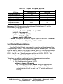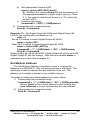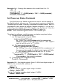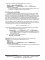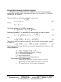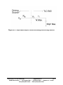
1
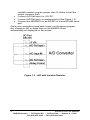
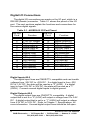
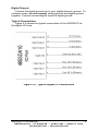
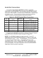
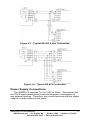
RS-485 Data Acquisition Module Model 485SDA10 Document No. 485SDA103798 This product Designed and Manufactured In Ottawa, Illinois USA of domestic and imported parts by B&B Electronics Mfg. Co. Inc. 707 Dayton Rd. -- P.O. Box 1040 -- Ottawa, IL 61350 PH (815) 433-5100 -- FAX (815) 434-7094 Internet: http://www.bb-elec.com [email protected] [email protected] 1995 B&B Electronics -- Revised September 1998 485SDA103798 Manual Cover Page B&B Electronics -- 707 Dayton Rd. -- PO Box 1040 -- Ottawa, IL 61350 PH (815) 433-5100 -- FAX (815) 434-7094 Table of Contents Chapter 1- Introduction ...........................................1 485SDA10 Features ...................................................... 1 Packing List ................................................................... 2 Software Installation ...................................................... 2 DOS ...................................................................................... 2 Windows 3.11 ....................................................................... 3 Windows 9x and Windows NT.............................................. 3 Uninstall......................................................................... 3 Windows 3.11 ....................................................................... 3 Windows 9x & Windows NT ................................................. 3 Getting Started .............................................................. 3 485SDA10 Specifications .............................................. 5 Analog to Digital Converter................................................... 5 5 Volt Reference ................................................................... 5 Digital Inputs ......................................................................... 5 Digital Outputs ...................................................................... 5 Power Supply........................................................................ 5 Communications................................................................... 5 Factory Default Settings ....................................................... 5 Chapter 2 - Connections..........................................6 A/D Connections............................................................ 6 A/D Inputs #0-10................................................................... 6 A/D Ref Input + ..................................................................... 6 A/D Ref Input - ...................................................................... 7 Analog Ground...................................................................... 7 Typical Connections ............................................................. 7 Digital I/O Connections .................................................. 8 Digital Inputs #0-2................................................................. 8 Digital Outputs #0-2 .............................................................. 8 Digital Ground....................................................................... 9 Typical Connections ............................................................. 9 Serial Port Connections ............................................... 10 Power Supply Connections.......................................... 11 Chapter 3 - Commands..........................................12 Syntax ......................................................................... 13 Reading A/D Channels Command............................... 13 Reading Digital I/O Command ..................................... 15 Set Digital Output Command ....................................... 16 Set Module Address Command ................................... 16 Set Power-up States Command .................................. 17 485SDA103798 Manual Table of Contents B&B Electronics -- 707 Dayton Rd. -- PO Box 1040 -- Ottawa, IL 61350 PH (815) 433-5100 -- FAX (815) 434-7094 i Set Turn-around Delay Command ............................... 17 Read Module Configuration Command........................ 17 Chapter 4 - A/D .......................................................19 Sampling Rate ............................................................. 19 A/D Input Range .......................................................... 19 Reference Inputs ......................................................... 19 Data Range ................................................................. 20 Converting Data........................................................... 20 Chapter 5 - Software ..............................................22 Read A/D Command ................................................... 22 Read Digital I/O Command.......................................... 23 Set Digital Output States ............................................. 24 Set Module Address .................................................... 25 Set Power-up States Command .................................. 26 Set Turn-around Delay ................................................ 27 Read Module Configuration ......................................... 28 Appendix A: Adding Data Field Confirmation.... A-1 Appendix B: Analog Input Impedance................ B-1 Appendix C: Decimal to HEX to ASCII Table .... C-1 Figures FIGURE 1.1 - 485SDA10 UNIT ...................................................................... 1 FIGURE 1.2 - GENERAL BLOCK DIAGRAM ............................................... 2 FIGURE 1.3 - A/D WITH VARIABLE RESISTOR ......................................... 4 FIGURE 2.1 - TYPICAL 0-5V A/D CONNECTION ....................................... 7 FIGURE 2.2 - TYPICAL DIGITAL I/O CONNECTIONS ............................... 9 FIGURE 4.1 - A/D CONVERTER DATA RANGE........................................ 20 FIGURE B-1 - EQUIVALENT INPUT CIRCUIT INCL/DRIVING SOURCEB-3 Tables TABLE 2.1 - 485SDA10 I/O PORT PINOUT ...................................... 8 TABLE 2.2 - RS-485 TERMINAL BLOCK CONNECTIONS .......... 10 TABLE 3.1 - 485SDA10 COMMANDS ............................................. 12 TABLE 3.2 - EQUIVALENT VALUES ............................................. 13 TABLE 3.3 - READ A/D RESPONSE................................................ 14 TABLE 3.4 - READ DIGITAL I/O RESPONSE FOR OUTPUTS..... 15 TABLE 3.5 - READ DIGITAL I/O RESPONSE FOR INPUTS......... 15 TABLE 3.6 - SET DIGITAL OUTPUT DATA BYTE VALUES ...... 16 ii Table of Contents 485SDA103798 Manual B&B Electronics -- 707 Dayton Rd. -- PO Box 1040 -- Ottawa, IL 61350 PH (815) 433-5100 -- FAX (815) 434-7094 TABLE 5.1 - DIGITAL I/O MASK VALUES.................................... 24 TABLE A-1 EXTENDED COMMANDS........................................ A-2 TABLE C-1: DECIMAL TO HEX TO ASCII TABLE.................... C-1 485SDA103798 Manual Table of Contents B&B Electronics -- 707 Dayton Rd. -- PO Box 1040 -- Ottawa, IL 61350 PH (815) 433-5100 -- FAX (815) 434-7094 iii Chapter 1- Introduction 485SDA10 Features The 485SDA10 is a general purpose control module which operates through an RS-485 interface. The 485SDA10 offers 11 channels of 10-bit A/D (analog to digital), 3 digital inputs and 3 digital outputs. With these features, the module can be used to sense a variety of external conditions and to control a variety of devices. The 11 A/D channels allow you to measure voltages from 0 to 5 Volts. The 3 digital inputs and 3 digital outputs are CMOS/TTL compatible. The A/D and digital I/O lines are available through a DB25S (female) connector. The 485SDA10 connects to the host computer’s RS-485 or RS-422 serial port using terminal blocks. The address and turnaround delays are software programmable to allow use of multiple devices or connection to existing systems. The unit automatically detects baud rates from 1200 to 9600. A data format of 8 data bits, 1 stop bit and no parity is used. Configuration parameters are stored in non-volatile memory. The configuration parameters consist of the module address, communication turn-around delay, and digital output power-up states. Figure 1.1 - 485SDA10 Unit 485SDA103798 Manual B&B Electronics -- 707 Dayton Rd. -- PO Box 1040 -- Ottawa, IL 61350 PH (815) 433-5100 -- FAX (815) 434-7094 1 Figure 1.2 - General Block Diagram Packing List Examine the shipping carton and contents for physical damage. The following items should be in the shipping carton: • 485SDA10 unit • One 485SDA10 3.5” disk • This instruction manual • RS-485/422 Application Note If any of these items are damaged or missing contact B&B Electronics immediately. Software Installation The 485SDA10 comes with several useful programs such as a data logging utility, a demonstration program, etc. The installation for the SDA Logger is different depending on the platform you install it to. Please use the one appropriate to your system. DOS 1. Place the disk in drive A. 2. Type A: and press the <ENTER> key. 3. Type INSTALL and press the <ENTER> key. 4. Follow the instructions given by the program. 2 485SDA103798 Manual B&B Electronics -- 707 Dayton Rd. -- PO Box 1040 -- Ottawa, IL 61350 PH (815) 433-5100 -- FAX (815) 434-7094 Windows 3.11 1. Insert SDA Logger installation disk in your floppy drive. 2. Click the File Manager button. 3. Select the floppy drive containing the SDA Logger installation disk. 4. Double click the Setup.exe icon when it appears. 5. Follow the installation instructions as prompted. Windows 9x and Windows NT 1. Insert the SDA Logger installation disk in your floppy drive. 2. Click Start | Run. 3. Click the Browse button and choose the floppy drive containing the SDA Logger installation disk. 4. Double click the Setup.exe icon when it appears. 5. Click the OK button to run the Setup.exe program. 6. Follow the installation instructions as prompted. Uninstall Uninstall for the SDA Logger version is different for each Windows operating system. Below are the methods for uninstalling the SDA Logger. Windows 3.11 1. Open the File Manager in the Control Panel. 2. Click the drive that SDA Logger was installed to. 3. Click the SDA16 directory. 4. Double click the UNWISE.EXE. 5. Follow the Uninstall Wizard. Windows 9x & Windows NT 1. Open Start | Settings | Control Panel. 2. Open ADD/REMOVE PROGRAMS. 3. Click SDA LOGGER. 4. Click the Add/Remove button. 5. Follow the Uninstall Wizard. Getting Started This section will provide a quick example using the 485SDA10 and the demonstration program. If you experience any problems, refer to Chapter 2 for more precise information on connections. The demo program continually reads the A/D inputs and the digital I/O. The states of the digital outputs can be toggled using F2, F3, and F4. The serial port is configured for 9600 baud, 8 data bits, no parity, and 1 stop bit. The program supports standard addresses and IRQ’s for COM1 and COM2. • Connect a 0 to 5V DC analog device to A/D input #0, or you can connect a variable resistor as shown in Figure 1.3. The 485SDA103798 Manual B&B Electronics -- 707 Dayton Rd. -- PO Box 1040 -- Ottawa, IL 61350 PH (815) 433-5100 -- FAX (815) 434-7094 3 variable resistor must be greater than 1k Ohms to limit the output current to 5mA. • Connect A/D Ref Input+ to +5V DC. • Connect A/D Ref Input- to analog ground (See Figure 1.3). • Connect the 485SDA10 to an RS-422 or 4-wire RS-485 serial port. Once your connections have been made, run the demo program. Any change in A/D or digital lines on the 485SDA10 will automatically be displayed on the screen. Figure 1.3 - A/D with Variable Resistor 4 485SDA103798 Manual B&B Electronics -- 707 Dayton Rd. -- PO Box 1040 -- Ottawa, IL 61350 PH (815) 433-5100 -- FAX (815) 434-7094 485SDA10 Specifications Analog to Digital Converter Resolution: 10 bit Channels: 11 Reference Range: 5.0V DC max. (4.888 mV per bit) 2.5V DC min. (2.444 mV per bit) A/D Ref. Input 0V DC to 2.5V DC A/D Ref. Input + 2.5V DC to 5.0V DC Input Voltage Range: -0.3V DC to 5.3V DC Total Unadjusted Error: +/- 1 LSB max. A/D input channels must be driven from a source impedance less than 1kΩ. 5 Volt Reference Output Voltage: 4.975 to 5.025V DC (5.0V DC typ.) Accuracy: +/- 0.5 % Output Current: 5mA max. Digital Inputs Channels: 3 Voltage Range: -30V DC to 30V DC Low Voltage: -30V DC to 1.0V DC High Voltage: 2.0V DC to 30V DC Leakage Current: 1 µA max. Digital Outputs Channels: 3 Low Voltage: 0.6V DC @ 8.7mA High Voltage: 4.3V DC @ -5.4mA Power Supply Input Voltage: 7V DC to 18V DC @ 30mA (Doesn’t include the power consumption of external devices.) Communications Standard: RS-422/485 Addresses: 256 Turn-around Delay: Software programmable from 0 to 255 character transmission times. (1 char. trans. time @ 9600 baud = 1ms) Baud Rate: 1200 to 9600 (automatic detection) Format: 8 data bits, 1 stop bit, no parity Connector: DB-25S (female) Factory Default Settings Address: ACSII “0” (48 decimal or 30h) Turn-around Delay: 1 Power-up States: 0 485SDA103798 Manual B&B Electronics -- 707 Dayton Rd. -- PO Box 1040 -- Ottawa, IL 61350 PH (815) 433-5100 -- FAX (815) 434-7094 5 Chapter 2 - Connections This chapter will cover the connections required for the 485SDA10. There are four sets of connections: • A/D converter • Digital I/O • Serial port • Power supply Do not make any connections to the 485SDA10 until you have read this chapter. CAUTION: When making electrical connections it is important to power down the devices being connected. If this is not possible, precautions must be taken to ensure electrical specifications are not exceeded. NOTE: If you do not intend to use a section (A/D or I/O), it is still important to read each one. A/D Connections The A/D connections are made on the I/O port, which is a DB25S (female) connector. Table 2.1 shows the pinout of the I/O port. The next sections explain the functions and connections for the various analog signals. A/D Inputs #0-10 These are the analog input channels. The analog data that is read from the 485SDA10 is related to the voltage on these pins. Connect your devices to the analog input channels. Voltages on these inputs must remain between 0 and 5.0V DC. Connect unused A/D inputs to analog ground. A/D Ref Input + The voltage connected to this pin determines the upper end of the input voltage range. For proper operation, this pin must be connected to a DC voltage between +2.5 and +5.0 Volts. The 485SDA10 provides a 5.0V +/-0.5% reference on pin 17. The 5V reference can be used if you require a 0 to 5V DC input range. If your application requires a better reference voltage or a different input range, you must supply the appropriate reference to the A/D Ref Input+ pin. This voltage must be at least 2.5V greater than A/D Ref Input-. Bypassing the A/D Ref Input+ pin with 0.01µF ceramic and 10µF tantalum capacitors to analog ground will decrease noise levels. 6 485SDA103798 Manual B&B Electronics -- 707 Dayton Rd. -- PO Box 1040 -- Ottawa, IL 61350 PH (815) 433-5100 -- FAX (815) 434-7094 A/D Ref Input The voltage connected to this pin determines the low end of the input voltage range. For proper operation, this pin must be connected to a DC voltage between 0 and +2.5 Volts. Typically, this is connected to your device’s ground and analog ground (0V). Analog Ground This pin should be connected to your analog device’s ground. If ground (0V) is the low end of your input voltage range, A/D Ref Input- should be connected to this pin. To minimize noise, do not connect analog ground and digital ground together. Connect unused A/D inputs to analog ground. Typical Connections Figure 2.1 shows the typical connections of the 485SDA10 for a 0 to 5V DC input range. Figure 2.1 - Typical 0-5V A/D Connection 485SDA103798 Manual B&B Electronics -- 707 Dayton Rd. -- PO Box 1040 -- Ottawa, IL 61350 PH (815) 433-5100 -- FAX (815) 434-7094 7 Digital I/O Connections The digital I/O connections are made on the I/O port, which is a DB-25S (female) connector. Table 2.1 shows the pinout of the I/O port. The next sections explain the functions and connections for the various digital signals. Table 2.1 - 485SDA10 I/O Port Pinout DB-25S DB-25S Pin # Function Pin # Function 1 GND 14 Digital Output #0 2 +12V DC Output* 15 Digital Output #1 3 Digital Input #0 16 Digital Output #2 4 Digital Input #1 17 +5V DC Output 5 Digital Input #2 18 A/D Ref. Input + 6 Digital GND 19 A/D Ref. Input 7 Analog GND 20 No connection 8 A/D Input #0 21 A/D Input #6 9 A/D Input #1 22 A/D Input #7 10 A/D Input #2 23 A/D Input #8 11 A/D Input #3 24 A/D Input #9 12 A/D Input #4 25 A/D Input #10 13 A/D Input #5 *Actual output is equal to power supply input minus 0.7V DC Digital Inputs #0-2 The digital input lines are CMOS/TTL compatible and can handle voltages from -30V DC to +30V DC. If a digital input is from -30V DC to 1.0V DC, the state will be read as a “0” (LOW). If a digital input is from 2.0V DC to 30V DC, the state will be read as a “1” (HIGH). Connect unused digital inputs to digital ground. Digital Outputs #0-2 The digital output lines are CMOS/TTL compatible. A digital output that is set to a “0” (LOW) will output a voltage from 0 to 0.6V DC. A digital output that is set to a “1” (HIGH) will output a voltage from 4.3V DC to 5.0V DC. Refer to Chapter 1, Specifications, for more information. Unused digital output lines should be left open. 8 485SDA103798 Manual B&B Electronics -- 707 Dayton Rd. -- PO Box 1040 -- Ottawa, IL 61350 PH (815) 433-5100 -- FAX (815) 434-7094 Digital Ground Connect the digital ground pin to your digital device's ground. To minimize noise, do not connect analog ground and digital ground together. Connect unused digital inputs to digital ground. Typical Connections Figure 2.2 shows the typical connections of the 485SDA10 for the digital I/O lines. Figure 2.2 - Typical Digital I/O Connections 485SDA103798 Manual B&B Electronics -- 707 Dayton Rd. -- PO Box 1040 -- Ottawa, IL 61350 PH (815) 433-5100 -- FAX (815) 434-7094 9 Serial Port Connections To communicate with the 485SDA10 module, it must be connected to an RS-422/RS-485 serial port. The 485SDA10 works with 2-wire or 4-wire RS-485. The unit automatically detects baud rates from 1200 to 9600. A data format of 8 data bits, 1 stop bit and no parity is used. Connections are made using terminal blocks. Table 2.2 shows the terminal blocks and their functions. Table 2.2 - RS-485 Terminal Block Connections TB Label Signal 485SDA1 0 Function TD(A) Transmit Data (A) Output TD(B) Transmit Data (B) Output RD(A) Receive Data (A) Input RD(B) Receive Data (B) Input GND Ground - +12V +12 V DC Power Input Notes Connection is required. [Loop to RD(A) for 2-wire hookup] Connection is required. [Loop to RD(B) for 2-wire hookup] Connection is required. [Loop to RD(A) for 2-wire hookup] Connection is required. [Loop to RD(B) for 2-wire hookup] Connection for Signal GND and Power Supply GND. Connection is required. A typical 2-wire RS-485 connection is shown in Figure 2.3 and a typical RS-422 (or RS-485) 4-wire is shown in Figure 2.4. NOTE: The 485SDA10 labels the data lines with “A” and “B” designators (per EIA RS-485 Specification). However, some RS485 equipment used “+” and “-“ as designators. In most cases the “A” line is the equivalent of the “-“ line and the “B” line is the equivalent of the “+” line. With an RS-485/422 system there are other factors that require consideration, such as termination and turn-around delay. For more information refer to the RS-485/422 Application Note (included in packing). 10 485SDA103798 Manual B&B Electronics -- 707 Dayton Rd. -- PO Box 1040 -- Ottawa, IL 61350 PH (815) 433-5100 -- FAX (815) 434-7094 Figure 2.3 - Typical RS-485 2-wire Connection Figure 2.4 - Typical RS-422 Connection Power Supply Connections The 485SDA10 requires 7 to 18 V DC at 30mA. Remember that the 30mA requirement doesn’t include the power consumption of any external devices. Therefore, any current sourced with the digital outputs must be added to this value. 485SDA103798 Manual B&B Electronics -- 707 Dayton Rd. -- PO Box 1040 -- Ottawa, IL 61350 PH (815) 433-5100 -- FAX (815) 434-7094 11 Chapter 3 - Commands There are only three commands required to control the 485SDA10: • Read A/D command • Read digital I/O command • Set output states command There are four commands used to configure the module: • Set power-up states command • Set turn-around delay command • Set module address command • Read module configuration command The command string consists of four bytes. Some commands require an additional data byte. For information on adding data field confirmation to the data fields refer to Appendix A. See Table 3.1. Table 3.1 - 485SDA10 Commands Function Command Response Read A/D Channels !{addr}RA{#} Read Digital I/O Set Output States Set Module Address Set Power-up States Set Turn-around Delay Read Configuration !{addr}RD !{addr}SO{#} !{addr}SA{new addr} !{addr}SS{#} !{addr}SC{#} !{addr}RC {ch#msb}{ch#lsb} {ch(#-1)msb}... {ch0msb}{ch0lsb} {I/O states} no response no response no response no response {addr}{powerup states}{turn-around delay} NOTE: Each {...} represents one byte. Before going into the specifics of each command, it is important to understand that a byte has a value from 0 to 255 and can be represented in decimal (0 to 255), hexadecimal (00 to FF), or by an ASCII character. The commands in Table 3.1 are shown in ASCII, for example: ASCII !0RD 12 Hex <21><30><52><44> Decimal (33)(48)(82)(68) 485SDA103798 Manual B&B Electronics -- 707 Dayton Rd. -- PO Box 1040 -- Ottawa, IL 61350 PH (815) 433-5100 -- FAX (815) 434-7094 The decimal and hexadecimal equivalents of some ASCII characters are shown in Table 3.2. Notice that the ASCII representation of the character “0” does not have a value of 0. Refer to Appendix C for more ASCII, decimal, and hexadecimal equivalents. Table 3.2 - Equivalent Values ASCII Decimal Hexadecimal ! 0 A D O R S NUL SOH STX ETX EOT ENQ ACK BEL 33 48 65 68 79 82 83 0 1 2 3 4 5 6 7 21h 30h 41h 44h 4Fh 52h 53h 0h 1h 2h 3h 4h 5h 6h 7h Syntax The command string consists of four bytes. The first byte is the start of message byte. The start of message byte is always the “!” character. The second byte is the address byte. This byte allows each unit to have a unique address. The factory default address is the ASCII “0” (zero) character. The next two bytes are the command characters. These bytes are used to specify which command the module will execute. The read A/D and digital I/O commands require an additional data byte. _ _ _ Command Syntax: ! | | | | | | | | | Data Byte | | | 2nd Command Byte | | 1st Command Byte | Address Byte Start of Message Byte Reading A/D Channels Command 485SDA103798 Manual B&B Electronics -- 707 Dayton Rd. -- PO Box 1040 -- Ottawa, IL 61350 PH (815) 433-5100 -- FAX (815) 434-7094 13 The Read A/D channels command returns two bytes for each channel read. The two bytes represent the most significant byte (MSB) and least significant byte (LSB) of the reading. The MSB is received first, followed by the LSB. This command requires a data byte. The data byte is used to specify the number of the highest channel to be read. All channels less than this channel will be read as well. For example, if the data byte has a value of 6, then channels 0 to 6 will be read. The highest channel is read first. Command Syntax !{addr}RA{#} Where “{#}” is a byte that specifies the number of the highest channel to be read. See Table 3.3 Response Syntax {ch(#)MSB}{ch(#)LSB}{ch(#-1)MSB}...{ch0MSB}{ch0LSB} The most significant byte of the channel specified is received first. The least significant byte and the lower channels will follow in descending order. “{chxMSB}” and “{chxLSB}” represent the most and least significant bytes of the A/D conversion result. Table 3.3 - Read A/D Response # of Channels Specified Response Channels Returned Bytes decimal Hex ASCII (order of response) Returned 0 1 2 3 4 5 6 7 8 9 10 0 1 2 3 4 5 6 7 8 9 A NUL SOH STX ETX EOT ENQ ACK BEL BS HT LF Channel 0 Channels 1,0 Channels 2,1,0 Channels 3,2,..,0 Channels 4,3,..,0 Channels 5,4,..,0 Channels 6,5,..,0 Channels 7,6,..,0 Channels 8,7,..,0 Channels 9,8,..,0 Channels 10,9,..,0 2 4 6 8 10 12 14 16 18 20 22 NOTE: There are three test channels that can be read: Ref+, Ref-, and Ref+/2. Specify 13 (0Dh) to read Ref+, 12 (0Ch) to read Ref-, and 11 (0Bh) to read Ref+/2. 14 485SDA103798 Manual B&B Electronics -- 707 Dayton Rd. -- PO Box 1040 -- Ottawa, IL 61350 PH (815) 433-5100 -- FAX (815) 434-7094 Reading Digital I/O Command The Read Digital I/O command returns a byte which represents the states of the 3 digital input and 3 digital output states. Bits 3-5 correspond to the states of digital inputs 0-2. Bits 0-2 correspond to the states of digital outputs 0-2. If a bit is a 0 then the digital state of that digital I/O is LOW. If a bit is a 1 then the digital state of the I/O is HIGH. Refer to Table 3.4 and 3.5. Command Syntax !{addr}RD Unit Response {states} Where {states} is a byte in which Bits 0-2 corresponds to the current states of Digital Outputs 0-2 and Bits 3-5 corresponds to the current states of Digital Inputs 0-2. Table 3.4 - Read Digital I/O Response for Outputs Response Byte Digital Outputs Bit 2 Bit 1 Bit 0 #2 #1 #0 0 0 0 0 1 1 1 1 0 0 1 1 0 0 1 1 0 1 0 1 0 1 0 1 LOW LOW LOW LOW HIGH HIGH HIGH HIGH LOW LOW HIGH HIGH LOW LOW HIGH HIGH LOW HIGH LOW HIGH LOW HIGH LOW HIGH Table 3.5 - Read Digital I/O Response for Inputs Response Byte Digital Inputs Bit 5 Bit 4 Bit 3 #2 #1 #0 0 0 0 0 1 1 1 1 0 0 1 1 0 0 1 1 0 1 0 1 0 1 0 1 LOW LOW LOW LOW HIGH HIGH HIGH HIGH LOW LOW HIGH HIGH LOW LOW HIGH HIGH LOW HIGH LOW HIGH LOW HIGH LOW HIGH 485SDA103798 Manual B&B Electronics -- 707 Dayton Rd. -- PO Box 1040 -- Ottawa, IL 61350 PH (815) 433-5100 -- FAX (815) 434-7094 15 Set Digital Output Command The Set Digital Output command is used to set the states of the 3 digital output lines. This command requires a data byte. The data byte is used to specify the output states. Bits 0-2 correspond to the states of digital outputs 0-2. If a bit is a 0 then the output will be set LOW. If a bit is a 1 then the output will be set HIGH. Refer to Table 3.6. NOTE: This command ignores Bits 3-7 of the data byte. Command Syntax !{addr}SO{states} Where {states} is a byte in which Bits 0-2 correspond to the outputs states of Digital Outputs 0-2 Unit Response no response Bit 2 0 0 0 0 1 1 1 1 Table 3.6 - Set Digital Output Data Byte Values Data Byte Digital Outputs Bit 1 Bit 0 #2 #1 #0 0 0 1 1 0 0 1 1 0 1 0 1 0 1 0 1 LOW LOW LOW LOW HIGH HIGH HIGH HIGH LOW LOW HIGH HIGH LOW LOW HIGH HIGH LOW HIGH LOW HIGH LOW HIGH LOW HIGH Set Module Address Command The Set Module Address command is used to change the address of a 485SDA10. This command requires a data byte. The data byte is used to specify the new address of the unit. The address of a module is stored in non-volatile memory. Command Syntax !{addr}SA{new address} Response Syntax no response Where {addr} is the current address of the module and {new address} is a byte representing the new address. 16 485SDA103798 Manual B&B Electronics -- 707 Dayton Rd. -- PO Box 1040 -- Ottawa, IL 61350 PH (815) 433-5100 -- FAX (815) 434-7094 Set Power-up States Command The Set Power-up States command is used to set the states of the digital outputs at power-up. This command requires a data byte. The data byte is used to specify the power-up output states. Bits 0-2 correspond to the power-up states of digital outputs 0-2. If a bit is a 0 then the output will be set LOW at power-up. If a bit is a 1 then the output will be set HIGH at power-up. Refer to Table 3.6. NOTE: This command ignores bits 3-7 of the data byte. Command Syntax !{addr}SS{states} Response Syntax no response Where {states} is a byte in which Bits 0-2 correspond to the power-up states of Digital Outputs 0-2 Set Turn-around Delay Command The Set Turn-around Delay command sets the amount of time the 485SDA10 waits to respond after executing a command. This delay is necessary when two RS-485 transmitters are sharing a pair of wires to ensure that two transmitters are not enabled at the same time. Refer to B&B Electronics’ free RS-422/RS-485 Application Note for more information on RS-422/485. The turn-around delay is stored in non-volatile memory. This command requires a data byte. The data byte is used to specify the turn-around delay. One unit of turn-around delay is equal to the transmission time of one character. The transmission time can be computed as follows: time = (1 / baud rate) * 10 Command Syntax !{addr}SC{delay} Response Syntax no response Where {delay} is a byte used to specify the turn-around delay. Read Module Configuration Command The Read Module Configuration command reads the 485SDA10’s address, power-up states, and turn-around delay (in that order). Command Syntax !{addr}RC Response Syntax 485SDA103798 Manual B&B Electronics -- 707 Dayton Rd. -- PO Box 1040 -- Ottawa, IL 61350 PH (815) 433-5100 -- FAX (815) 434-7094 17 {address}{states}{delay} Where {address} is a byte representing the module’s current address, {states} is a byte representing the module’s power-up states, and {delay} is a byte representing the module’s turn-around delay. 18 485SDA103798 Manual B&B Electronics -- 707 Dayton Rd. -- PO Box 1040 -- Ottawa, IL 61350 PH (815) 433-5100 -- FAX (815) 434-7094 Chapter 4 - A/D This chapter will deal with manipulating an A/D reading and cover some of the aspects that were not explained in the A/D Connections chapter. Sampling Rate The A/D converter has a conversion time of around 20 microseconds, however the sampling rate is limited by the serial communications. The maximum sampling rate for a single channel is around 120 samples per second (9600 baud). This rate drops to 25 samples per second when sampling all of the channels. When reading an A/D input, the 485SDA10 takes four readings and returns the average (0.5 and greater are rounded up) of these readings. This averaging filters out noise. A/D Input Range The A/D input range on the 485SDA10 is from 0 to +5V DC. If it is possible for your device to output a voltage that doesn’t fall in this range, steps must be taken to ensure that the voltage remains between 0 and +5V DC. Voltages outside this range will damage the unit. Reference Inputs The A/D reference inputs set the top and bottom of the data range. A/D Ref Input- sets the bottom of the data range. A/D Ref Input+ sets the top of the data range. Since these inputs are directly related to the data range, it is important that a precision reference is used. The 485SDA10 has a 5V DC +/- 0.5% reference available. The voltage on A/D Ref Input+ must be at least 2.5V DC greater than A/D Ref Input-. The voltage difference between A/D Ref Input+ and A/D Ref Input- is referred to as the Reference Range. Reference Range = (A/D Ref Input+) - (A/D Ref Input-) Typically A/D Ref Input- is connected to Analog ground and A/D Ref Input+ is connected to +5V DC. Figure 2.1 in Chapter 2 shows the typical connections for a reference range of 0 to 5V DC. 485SDA103798 Manual B&B Electronics -- 707 Dayton Rd. -- PO Box 1040 -- Ottawa, IL 61350 PH (815) 433-5100 -- FAX (815) 434-7094 19 Data Range The data range of the A/D converter is determined by A/D Ref Input+ and A/D Ref Input-. A/D Ref Input- sets the bottom of the data range. Any input voltage that is less than or equal to the A/D Ref Input- will be read as a zero. A/D Ref Input+ sets the top of the data range. Any input voltage that is greater than or equal to the A/D Ref Input+ will be read as a 1023 (3FFh). The data range is as follows: Data Range = (A/D Ref Input-) to (A/D Ref Input+) Data Range = 0 to 1023 Data Range = 0 to 3FFh Figure 4.1 shows the Data Range and A/D Ref Inputs relationship. Figure 4.1 - A/D Converter Data Range Converting Data The data read from the 485SDA10 A/D converter is directly related to the A/D input channel and the reference range (discussed in previous sections). The 485SDA10 has a 10-bit A/D converter. A 10-bit A/D has 1024 possible output values, 0 to 1023 (0 to 3FFh). These 1024 output values are divided into equal steps over the reference range. The size of each step can be computed as follows: Step size = (Reference Range) / 1023 20 485SDA103798 Manual B&B Electronics -- 707 Dayton Rd. -- PO Box 1040 -- Ottawa, IL 61350 PH (815) 433-5100 -- FAX (815) 434-7094 The step size is also referred to as the resolution. Once the step size is known, all that is needed to determine the voltage of an A/D input is the number of steps. The data returned from the 485SDA10 is the number of steps. The voltage at the A/D inputs can be calculated as follows: Voltage = (# of steps) * (Step size) Example 4.1 - Assume: A/D Ref. Input + = 5.0V DC and A/D Ref.Input - = 0V DC. Therefore: Reference Range = (A/D Ref. Input +) - (A/D Ref. Input -) Reference Range = (5.0V DC) - (0V DC) Reference Range = 5.0V DC Step size = (Reference Range) / 1023 Step size = (5.0V DC) / 1023 Step size = 4.8876 millivolts Example #1: A/D reading = 1023 (3FFH) A/D voltage = reading * step size A/D voltage = 1023 * 4.8876 millivolts A/D voltage = 5.0 Volts Example #2: A/D reading = 0 A/D voltage = 0 * 4.8876 millivolts A/D voltage = 0 Volts Example #3: A/D reading = 675 (2A3H) A/D voltage = 675 * 4.8876 millivolts A/D voltage = 3.2991 Volts 485SDA103798 Manual B&B Electronics -- 707 Dayton Rd. -- PO Box 1040 -- Ottawa, IL 61350 PH (815) 433-5100 -- FAX (815) 434-7094 21 Chapter 5 - Software This chapter covers programming techniques such as constructing a command string, receiving data and manipulating data. The various steps and examples are shown in QuickBasic. If you are programming in another language, these sections can be used as a guideline for programming the 485SDA10. Read A/D Command The Read A/D channels command returns two bytes for each channel read. The two bytes represent the most significant byte (MSB) and least significant byte (LSB) of the reading. The MSB is received first, followed by the LSB. This command requires a data byte. The data byte is used to specify the number of the highest channel to be read. All channels less than this channel will be read as well. The steps to reading an A/D command are given below: 1. Constructing the command string: Command$ = “!” + CHR$(addr) + “RA” + CHR$(channel) The value of channel is equal to the highest channel to be read. 2. Transmitting the command string: Print #1, Command$; 3. Receiving the data: MSB$ = INPUT$(1, #1) LSB$ = INPUT$(1, #1) 4. Manipulating the data: reading = (ASC(MSB$) * 256) + ASC(LSB$) The value of reading is the result of the A/D conversion. 5. Repeat Steps 3 & 4 until each channel has been completed. Example 5.1 - Read A/D channels 1 and 0 of the module with an address of 5. channel = 1 addr = 5 Command$ = “!” + CHR$(addr) + “RA” + CHR$(channel) Print #1, Command$; 22 485SDA103798 Manual B&B Electronics -- 707 Dayton Rd. -- PO Box 1040 -- Ottawa, IL 61350 PH (815) 433-5100 -- FAX (815) 434-7094 ‘Get the value of channel 1 MSB$ = INPUT$ (1, #1) LSB$ = INPUT$ (1, #1) reading1 = (ASC(MSB$) * 256) + ASC(LSB$) ‘Get the value of channel 0 MSB$ = INPUT$ (1, #1) LSB$ = INPUT$ (1, #1) reading0 = (ASC(MSB$) * 256) + ASC(LSB$) The value of reading1 is the result of the A/D conversion on channel 1. The value of reading0 is the result of the A/D conversion on channel 0. Read Digital I/O Command The Read Digital I/O command returns a byte which represents the states of the 3 digital input and 3 digital output states. Bits 3-5 correspond to the states of digital inputs 0-2, and bits 0-2 correspond to the states of digital outputs 0-2. If a bit is a 0 then the digital state of that digital I/O is LOW. If a bit is a 1 then the digital state of the I/O is HIGH. The steps to reading a digital I/O command are given below: 1. Constructing the command string: Command$ = “!” + CHR$(addr) + “RD” 2. Transmitting the command string: Print #1, Command$; 3. Receiving the data: Reply$ = INPUT$ (1, #1) 4. Manipulating the data: states = ASC(Reply$) 5. Determining an I/O’s status status = states AND mask 6. Repeat Step 5 until the status of each I/O has been determined. By “ANDing” the value of states with the appropriate mask of an I/O line, the status of can be determined. If status is equal to zero then the I/O line is LOW. If status is not equal to zero then the I/O line is HIGH. Table 5.1 shows the mask values for each I/O. 485SDA103798 Manual B&B Electronics -- 707 Dayton Rd. -- PO Box 1040 -- Ottawa, IL 61350 PH (815) 433-5100 -- FAX (815) 434-7094 23 Table 5.1 - Digital I/O Mask Values Mask Values I/O Line Hexadecimal Decimal Digital Output #0 Digital Output #1 Digital Output #2 Digital Input #0 Digital Input #1 Digital Input #2 1H 2H 4H 8H 10H 20H 1 2 4 8 16 32 Example 5.2 - Determining the status of Digital Input #1 of the module with and address of 10. mask = &H10 Command$ = “!” + CHR$(addr) + “RD” Print #1, Command$; Reply$ = INPUT$ (1, #1) states = ASC (Reply$) status = states AND mask If status is equal to zero then Digital Input #1 is LOW. If status is not equal to zero then Digital Input #1 is HIGH. Set Digital Output States The Set Digital Output command is used to set the states of the 3 digital output lines. This command requires a data byte. The data byte is used to specify the output states. Bits 0-2 correspond to the states of digital outputs 0-2. If a bit is a 0 then the output will be set LOW. If a bit is a 1 then the output will be set HIGH. NOTE: This command ignores Bits 3-7 of the data byte. The steps to setting the digital output states are given below: 1) Constructing the command string: a) Set Appropriate Outputs HIGH states = states OR mask By “ORing” the current states with the appropriate mask of a digital output (given in Table 5.1), the output’s data bit will be set to a “1” (which will be set HIGH). 24 485SDA103798 Manual B&B Electronics -- 707 Dayton Rd. -- PO Box 1040 -- Ottawa, IL 61350 PH (815) 433-5100 -- FAX (815) 434-7094 b) Set Appropriate Outputs LOW states = states AND (NOT(mask)) By “ANDing” the current states with the complement of the appropriate mask of a digital output (given in Table 5.1), the output’s data bit will be set to a “0” (which will be set LOW). c) Construct the string Command$ = “!0SO” + CHR$(states) 2) Transmitting the command string: Print #1, Command$; Example 5.3 - Set Digital Output #0 HIGH and Digital Output #2 LOW of the module with and address of 5. addr = 5 ‘ Set bit 0 of states to make Digital Output #0 HIGH states = states OR 1 ‘ Clear bit 2 of states to make Digital Output #2 LOW states = states AND (NOT(4)) Command$ = “!” + CHR$(addr) + “SO” + CHR$(states) Print #1, Command$; Digital Output #0 will be set HIGH. Digital Output #2 will be set LOW. Digital Output #1 will not change. Note that the variable states is assumed to be value from Example 5.2. Set Module Address The Set Module Address command is used to change the address of a 485SDA10. This command requires a data byte. The data byte is used to specify the new address of the unit. The address of a module is stored in non-volatile memory. The steps to setting a module address are given below: 1) Constructing the command string: Command$ = “!” + CHR$(addr) + “SO” + CHR$(newaddr) Where {addr} is the current address of the module and {new address} is a byte representing the new address. 2) Transmitting the command string: Print #1, Command$ 485SDA103798 Manual B&B Electronics -- 707 Dayton Rd. -- PO Box 1040 -- Ottawa, IL 61350 PH (815) 433-5100 -- FAX (815) 434-7094 25 Example 5.4 – Change the address of a model from 5 to 10. addr = 5 newaddr = 10 Command$ = “!” + CHR$(addr) + “SA” + CHR$(newaddr) Print #1, Command$ Set Power-up States Command The Set Power-up States command is used to set the states of the digital outputs at power-up. This command requires a data byte. The data byte is used to specify the power-up output states. Bits 0-2 correspond to the power-up states of digital outputs 0-2. If a bit is a 0 then the output will be set LOW at power-up. If a bit is a 1 then the output will be set HIGH at power-up. Refer to Table 3.6. NOTE: This command ignores bits 3-7 of the data byte. The steps to setting a module’s power up states are given below: 1) Construct the command string: a) Set appropriate outputs HIGH states = states OR mask By “ORing” the current states with the appropriate mask of a digital output given in Table 5.1, the output’s data bit will be set to a “1” (HIGH). b) Set appropriate outputs LOW states = states AND (NOT(mask)) By “ANDing” the current states with the complement of the appropriate mask of a digital output given in Table 5.1, the output’s data bit will be set to a “0” (LOW). c) Construct the string Command$ = “!” + CHR$(addr) + “SS” + CHR$(states) Where addr is the module’s address. 2) Transmitting the command string: Print #1, Command$ Example 5.5 – Set digital outputs 0 and 1 HIGH and digital output 2 LOW on the module with address 5. addr = 5 states = 0 ‘ Set bit 0 of states to make digital output 0 HIGH states = states OR 1 ‘ Set bit 1 of states to make digital output 1 HIGH states = states OR 2 26 485SDA103798 Manual B&B Electronics -- 707 Dayton Rd. -- PO Box 1040 -- Ottawa, IL 61350 PH (815) 433-5100 -- FAX (815) 434-7094 ‘ Clear bit 2 of states to make digital output 2 LOW states = states AND (NOT(4)) Command$ = “!” + CHR$(addr) + “SS” + CHR$(states) Print #1, Command$ At power-up digital output 0 will be HIGH, digital output 1 will be HIGH, and digital output 2 will be LOW. Set Turn-around Delay The Set Turn-around Delay command sets the amount of time the 485SDA10 waits to respond after executing a command. This delay is necessary when two RS-485 transmitters are sharing a pair of wires to ensure that two transmitters are not enabled at the same time. Refer to B&B Electronics’ free RS-422/RS-485 Application Note for more information on RS-422/485. The turn-around delay is stored in non-volatile memory. This command requires a data byte. The data byte is used to specify the turn-around delay. One unit of turn-around delay is equal to the transmission time of one character. This transmission time can be computed as follows: time = (1 / baud rate) * 10 The steps to setting a module’s turn-around delay are given below: 1) Constructing the command string: Command$ = “!” + CHR$(addr) + “SC” + CHR$(delay) Where addr is the module’s address and delay is the turnaround delay. Refer to Chapter 3 for more information on turn-around delay. 2) Transmitting the command string: Print #1, Command$ Example 5.6 – Set the turn-around delay on the module with address 5 to 100 character transmission times. addr = 5 delay = 100 Command$ = “!” + CHR$(addr) + “SC” + CHR$(delay) Print #1, Command$ The module at address 5 will now have a turn-around delay of 100 character transmission times. 485SDA103798 Manual B&B Electronics -- 707 Dayton Rd. -- PO Box 1040 -- Ottawa, IL 61350 PH (815) 433-5100 -- FAX (815) 434-7094 27 Read Module Configuration The Read Module Configuration command reads the 485SDA10’s address first, then the power-up states, and finally the turn-around delay. The steps to reading a module’s configuration are given below: 1) Constructing the command string: Command$ = “!” + CHR$(addr) + “RC” Where addr is the module’s address. 2) Transmitting the command string: Print #1, Command$ 3) Receiving the address data: Reply$ = INPUT$(1,#1) 4) Determining the address: address = ASC(Reply$) 5) Receiving the power-up states data: Reply$ = INPUT$(1,#1) 6) Determining the power-up states: states = ASC(Reply$) Refer to Read Digital I/O earlier in this chapter for the steps to determine the status of individual output states. 7) Receiving the turn-around delay data: Reply$ = INPUT$ (1,#1) 8) Determining the turn-around delay: delay = ASC(Reply$) Example 5.7 – Determining the configuration of the module with an address of 10. addr = 10 Command$ = “!” + CHR$(addr) + “RC” Print #1, Command$ ‘ Determine the module’s address Reply$ = INPUT$ (1,#1) address = ASC(Reply$) ‘ Determine the module’s power-up states Reply$ = INPUT$ (1,#1) states = ASC(Reply$) ‘ Determine the module’s turn-around delay Reply$ = INPUT$ (1,#1) delay = ASC(Reply$) 28 485SDA103798 Manual B&B Electronics -- 707 Dayton Rd. -- PO Box 1040 -- Ottawa, IL 61350 PH (815) 433-5100 -- FAX (815) 434-7094 Appendix A: Adding Data Field Confirmation With serial communications in a laboratory environment, the possibility of a communication error occurring is minimal. However, in a harsh or an industrial environment the possibility increases. A communication error occurs when a bit transmitted as a “1” is received as a “0” or vice versa. If the 485SDA10 receives an error in one or more of the first four command characters (“!0xx”), the unit will not execute the command. However, if the 485SDA10 receives a communication error on a data byte (channel byte for Read Analog command or state byte for Set Output State command), the command will be executed since the unit has no way of knowing that there was an error. To provide the 485SDA10 with a way of detecting errors in the data fields, an additional set of commands can be used. This set of commands begins with the “#” (23h) character, instead of the “!” (21h) character. Refer to Table A-1. With these commands every data byte that is transmitted or received is followed by its complement. Example A.1 - To read A/D channel zero: Command syntax: #{addr}RA{00}{FF} Response syntax: {ch0 msb}{~ ch0 msb}{ch0 lsb} {~ ch0 lsb} Where “~” is used to indicate the “complement of.” If A/D channel 0 has a reading of 1, the following would be received: {00}{FF}{01}{FE} Where FFh is the complement of 0 and FEh is the complement of 1. The complement of number “x” can be calculated in QuickBasic as follows: comp = (NOT x) AND &HFF 485SDA103798 Manual Appendix A A-1 B&B Electronics -- 707 Dayton Rd. -- PO Box 1040 -- Ottawa, IL 61350 PH (815) 433-5100 -- FAX (815) 434-7094 Table A-1 Extended Commands Function Command Response Read A/D Channels #{addr}RA{x}{~x} Read Digital I/O Set Output States Set Module Address Set Power-up States Set Turn-around Delay Read Configuration #{addr}RD #{addr}SO{x}{~x} #{addr}SA{new addr}{~new addr} #{addr}SS{x}{~x} {chxmsb}{~chxmsb}{chxlsb} {~chxlsb}{ch(x-1)msb}... {ch0msb} {~ch0msb}{ch0lsb}{~ch0lsb} {I/O states}{~I/O states} no response no response no response #{addr}SC{x}{~x} no response #{addr}RC {addr}{~addr}{powerup states}{~powerup states}{turn-around delay}{~turn-around delay} Where “x” is the required data byte and “~” signifies the complement of the specified byte. A-2 Appendix A 485SDA103798 Manual B&B Electronics -- 707 Dayton Rd. -- PO Box 1040 -- Ottawa, IL 61350 PH (815) 433-5100 -- FAX (815) 434-7094 Appendix B: Analog Input Impedance When interfacing with an A/D converter, it is important that the device you are connecting can drive the A/D input. To determine if your device can drive an A/D input, there are three factors you must consider: • Output impedance of the device • Input impedance of A/D • A/D sampling time The goal is to have the voltage at the A/D input settle to a voltage close to the output voltage of the device in a time frame that is less than the A/D sampling time. (Close to means a value significantly less than the resolution of the A/D). If the voltage does not settle fast enough, errors will occur in the reading, resulting in a loss of resolution. The next section, titled “Simplified Analog Input Analysis,” contains information from Texas Instruments data sheet on the TLC1543. The TLC1543 is the A/D converter that is used on the 485SDA10. This section provides a simplified calculation which can be used to determine the maximum output impedance the device can have to settle the A/D input to a voltage within one half LSB. For the 485SDA10: t c = 100us Using this information: Rs ≤ 170 kΩ If the output impedance of your device is 170kΩ, you should figure an additional error of ½ LSB. It should be pointed out that this is a simplified analysis and there other several other factors that must be considered (pin capacitance, noise immunity, etc.). The data sheet for the TLC1543 states that “The driving source impedance should be less than or equal to 1kΩ.” B&B Electronics recommends placing a voltage follower between the 485SDA10 and any device with output source impedance greater than 1kΩ. 485SDA103798 Manual Appendix B B-1 B&B Electronics -- 707 Dayton Rd. -- PO Box 1040 -- Ottawa, IL 61350 PH (815) 433-5100 -- FAX (815) 434-7094 Simplified Analog Input Analysis Using the equivalent circuit in Figure B-1, the time required to charge the analog input capacitance from 0 to Vs within ½ LSB can be derived as follows: The capacitance charging voltage is given by Vc = Vs (1 − e where − tc Rt Ci ) (1) Rt = Rs + ri The final voltage to ½ LSB is given by Vc (1 2 LSB ) = Vs − (Vs 2048) (2) Equating equation 1 to equation 2 and solving for time tc gives Vs − (Vs 2048 ) = Vs (1 − e − tc Rt Ci ) (3) and (4) t c (1 2 LSB ) = Rt × Ci × ln( 2048 ) Therefore, with the values given the time for the analog input signal to settle is (5) t c (1 2 LSB ) = ( Rs + 1kΩ ) × 60 pF × ln( 2048) This time must be less than the converter sample time shown in the timing diagrams. VI = Input Voltage at A0 - A10 VS = External Driving Source Voltage RS = Source Resistance ri = Input Resistance Ci = Equivalent Input Capacitance *Driving source requirements: • Noise and distortion for the source must be equivalent to the resolution of the converter. • RS must be real at the input frequency. B-2 Appendix B 485SDA103798 Manual B&B Electronics -- 707 Dayton Rd. -- PO Box 1040 -- Ottawa, IL 61350 PH (815) 433-5100 -- FAX (815) 434-7094 Figure B-1. Equivalent Input Circuit Including the Driving Source 485SDA103798 Manual Appendix B B-3 B&B Electronics -- 707 Dayton Rd. -- PO Box 1040 -- Ottawa, IL 61350 PH (815) 433-5100 -- FAX (815) 434-7094 Appendix C: Decimal to HEX to ASCII Table Table C-1: Decimal to HEX to ASCII Table DECIMAL to HEX to ASCII CONVERSION TABLE DEC HEX ASCII KEY DEC HEX ASCII DEC HEX ASCII DEC HEX ASCII 0 0 NUL ctrl @ 32 20 SP 64 40 @ 96 60 ` 1 1 SOH ctrl A 33 21 ! 65 41 A 97 61 a 2 2 STX ctrl B 34 22 “ 66 42 B 98 62 b 3 3 ETX ctrl C 35 23 # 67 43 C 99 63 c 4 4 EOT ctrl D 36 24 $ 68 44 D 100 64 d 5 5 ENQ ctrl E 37 25 % 69 45 E 101 65 e 6 6 ACK ctrl F 38 26 & 70 46 F 102 66 f 7 7 BEL ctrl G 39 27 ' 71 47 G 103 67 g 8 8 BS ctrl H 40 28 ( 72 48 H 104 68 h 9 9 HT ctrl I 41 29 ) 73 49 I 105 69 i 10 A LF ctrl J 42 2A * 74 4A J 106 6A j 11 B VT ctrl K 43 2B + 75 4B K 107 6B k 12 C FF ctrl L 44 2C , 76 4C L 108 6C l 13 D CR ctrl M 45 2D - 77 4D M 109 6D m 14 E SO ctrl N 46 2E . 78 4E N 110 6E n 15 F SI ctrl O 47 2F / 79 4F O 111 6F o 16 10 DLE ctrl P 48 30 0 80 50 P 112 70 p 17 11 DC1 ctrl Q 49 31 1 81 51 Q 113 71 q 18 12 DC2 ctrl R 50 32 2 82 52 R 114 72 r 19 13 DC3 ctrl S 51 33 3 83 53 S 115 73 s 20 14 DC4 ctrl T 52 34 4 84 54 T 116 74 t 21 15 NAK ctrl U 53 35 5 85 55 U 117 75 u 22 16 SYN ctrl V 54 36 6 86 56 V 118 76 v 23 17 ETB ctrl W 55 37 7 87 57 W 119 77 w 24 18 CAN ctrl X 56 38 8 88 58 X 120 78 x 25 19 EM ctrl Y 57 39 9 89 59 Y 121 79 y 26 1A SUB ctrl Z 58 3A : 90 5A Z 122 7A z 27 1B ESC ctrl [ 59 3B ; 91 5B [ 123 7B { 28 1C FS ctrl \ 60 3C < 92 5C \ 124 7C | 29 1D GS ctrl ] 61 3D = 93 5D ] 125 7D } 30 1E RS ctrl ^ 62 3E > 94 5E ^ 126 7E ~ 31 1F US ctrl _ 63 3F ? 95 5F _ 127 7F DEL 485SDA103798 Manual Appendix C B&B Electronics -- PO Box 1040 -- Ottawa, IL 61350 PH (815) 433-5100 -- FAX (815) 434-7094 C-1 FEDERAL COMMUNICATIONS COMMISSION RADIO FREQUENCY INTERFACE STATEMENT Class A Equipment This equipment has been tested and found to comply with the limits for Class A digital device, pursuant to Part 15 of the FCC Rules. These limits are designed to provide reasonable protection against harmful interference when the equipment is operated in a commercial environment. This equipment generates, uses, and can radiate radio frequency energy and, if not installed and used in accordance with the instructions, may cause harmful interference to radio communications. Operation of this equipment in a residential area is likely to cause harmful interference, in which case the user will be required to correct the interference at personal expense. FCC Class A Equipment Statement