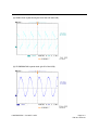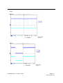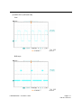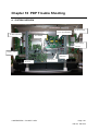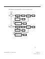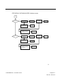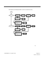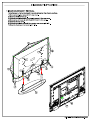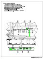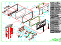
1
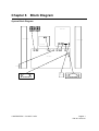
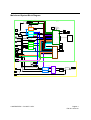
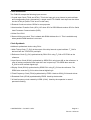
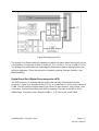
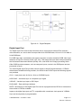
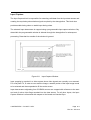
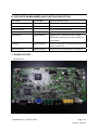
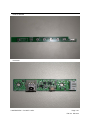
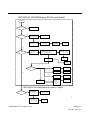
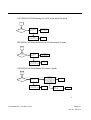
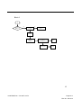
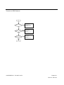
Service Manual Model #: VIZIO P50HDM V, Inc 320A Kalmus Drive Costa Mesa, CA 92626 TEL : +714-668-0588 FAX :+714-668-9099 -TOP Confidential - Table of Contents CONTENTS PAGE Sections 1. Features 1-1 2. Specifications 2-1 3. On Screen Display 3-1 4. Factory Preset Timings 4-1 5. Pin Assignment 5-1 6. BLOCK DIAGRAM 6-1 7. Main Board I/O Connections 7-1 8. Theory of Circuit Operation 8-1 9. Waveforms 9-1 10. Trouble Shooting 10-1 11. Spare Parts List 11-1 12. Complete Parts List 12-1 Appendix 1. Main Board Circuit Diagram 2. Main Board PCB Layout 3. Assembly Explosion Drawing Block Diagram VIZIO P50HDM Service Manual VINC Service Manual VIZIO P50HDM COPYRIGHT © 2000 V, INC. ALL RIGHTS RESERVED. IBM and IBM products are registered trademarks of International Business Machines Corporation. Macintosh and Power Macintosh are registered trademarks of Apple Computer, Inc. VINC and VINC products are registered trademarks of V, Inc. VESA, EDID, DPMS and DDC are registered trademarks of Video Electronics Standards Association (VESA). Energy Star is a registered trademark of the US Environmental Protection Agency (EPA). No part of this document may be copied, reproduced or transmitted by any means for any purpose without prior written permission from VINC. FCC INFORMATION This equipment has been tested and found to comply with the limits of a Class B digital device, pursuant to part 15 of the FCC Rules. These limits are designed to provide reasonable protection against harmful interference in a residential installation. This equipment generates, uses and can radiate radio frequency energy, and if not installed and used in accordance with the instructions, may cause harmful interference to radio communications. However, there is no guarantee that the interference will not occur in a particular installation. If this equipment does cause unacceptable interference to radio or television reception, which can be determined by turning the equipment off and on, the user is encouraged to try to correct the interference by one or more of the following measures -- reorient or relocate the receiving antenna; increase the separation between equipment and receiver; or connect the into an outlet on a circuit different from that to which the receiver is connected. FCC WARNING To assure continued FCC compliance, the user must use a grounded power supply cord and the provided shielded video interface cable with bonded ferrite cores. Also, any unauthorized changes or modifications to Amtrak products will void the user’s authority to operate this device. Thus VINC Will not be held responsible for the product and its safety. CE CERTIFICATION This device complies with the requirements of the EEC directive 89/336/EEC with regard to “Electromagnetic compatibility.” SAFETY CAUTION Use a power cable that is properly grounded. Always use the AC cords as follows – USA (UL); Canada (CSA); Germany (VDE); Switzerland (SEV); Britain (BASEC/BS); Japan (Electric Appliance Control Act); or an AC cord that meets the local safety standards. VIZIO P50HDM Service Manual Chapter 1 Features Wall-mountable New WIDE HD Plasma Panel:1366 x 768 (H x V) TruSurround XT sound system and DCDi by Faroujia video image High definition digital interface – HDMI HDCP supportive Multiple-screen display (picture-on-picture/picture-in-picture) Selectable picture mode 4-language On Screen Display 2 S-video and Composite video inputs 2 Component video inputs 2 HDMI inputs 6 audio stereos, 1 PC Mini-Jack Supporting DVI converted to HDMI Closed caption Gloss front bezel The thinnest model of this size: 99 mm CONFIDENTIAL – DO NOT COPY Page 1-1 File No. SG-0173 Chapter 2 Specification 1. OPTICAL CHARACTERISTICS Item Specification Display Pixels 1366 (H) x 768 (V) pixels Pixel Pitch 0.810 mm (H) X 0.810mm (V) Pixel Type Non-stripe Color Depth 1,024 (R) x 1,024 (G) x 1,024 (B) colors Active Display Area 1106.5 mm (H) x 622.1 mm(V) Brightness (panel spec) 1000 cd/m2 (Typical) (w/glass filter) Contrast ratio (panel spec) Min.300 cd/m 8000:1 (Typical, dark room) Color Coordinates (typical) White (Panel spec) x=0.300±0.02, y=0.300±0.02 White (w/glass filter) Warm (5400K) Standard (6500K) Cool (9300K): 2. INPUT SOURCE RGB Signal: H: support to 30-80KHz V: support to 60-85Hz Pixel Clock: support to 108MHz HDMI Signal: H: 15.734KHz V: 60Hz (480i) H: 31KHz V: 60Hz (480p) H: 45KHz V: 60Hz (720p) H: 33KHz V: 60Hz (1080i) S-Video: Video (Y): Analog 0.1Vp-p/75Ω Video (C): Analog 0.286p-p/75Ω CONFIDENTIAL – DO NOT COPY Page 2-1 File No. SG-0173 Composite Video signal: H: 15.734KHz Component signal: V: 60Hz (NTSC) YPbPr/YCbCr H: 15.734KHz V: 60Hz (NTSC-480i) H: 31KHz V: 60Hz(NTSC-480p) H: 45KHz V: 60Hz(NTSC-720p) H: 33KHz V: 60Hz(NTSC-1080i) 3. INPUT CONNECTORS Input Label SERVICE Connector Type RJ-11 x 1 Input Label ANALOG HD1 Connector Type YPb/Cb Pr/Cr RCA Jack x 3 Audio RCA Jack x 2 DIGITAL HD1 19 pin HDMI x 1 ANALOG HD2 Audio RCA Jack x 2 DIGITAL HD2 19 pin HDMI x 1 Audio RCA Jack x 2 AV1 Audio RCA Jack x 2 RGB D-sub 15 pin x 1 YPb/Cb Pr/Cr RCA Jackx 3 RCA Jack (CVBS) x 3 S-video 4 pin mini DIN x 1 AV2 Mini Jack x 1 (Audio RCA Jack (CVBS) x 3 S-video 4 pin mini DIN x 1 input) 4. OUTPUT CONNECTORS a. Audio RCA Jack x 2 b. 3.5mm Mini-jack earphone x 1 5. POWER SUPPLY Consumption: 550W MAXPower OFF: less than 3W 6. SPEAKER Output 8Ω/10W (max) X2 CONFIDENTIAL – DO NOT COPY Page 2-2 File No. SG-0173 7. ENVIRONMENT Operating a. Temperature: 0~40℃ b. c. Relative humidity: 20%~80% RH Altitude: 0~6,560 ft Non-operating a. Temperature: -20~60℃ b. c. Relative humidity: 10%~90% RH Altitude: 0~9,840 ft 8. DIMENSIONS a. Height: 871 mm b. Width: 1241mm c. Depth: 310 mm (with standard), 99 mm (without standard) 9. WEIGHT a. Net: 55.2 +/- 0.5 kgs b. Gross: 65.2 +/- 0.5 kgs CONFIDENTIAL – DO NOT COPY Page 2-3 File No. SG-0173 Chapter 3 On Screen Display Main unit button POWER MENU ▲ ▼ VOL-/W VOL+/X INPUT OSD Adjustment Mode Image Settings VIDEO Picture Mode(User, Vivid, Movie, Game, Sport) Brightness(0~100) Contrast(0~100) VIDEO Saturation(0~100) VIDEO Hue(-50~50) VIDEO Sharpness(0~24) Advanced VIDEO Noise Reduction VIDEO Motion(0~16) VIDEO Digital(0~64) VIDEO VIDEO Fleshtone Dynamic Off, High, Moderate, Low Contrast (0, 1, 2, 3) PC Auto Adjustment PC Image Position PC Phase PC Clocks / Line PC Color Temp PC CONFIDENTIAL – DO NOT COPY Warm(5400K) Page 3-1 File No. SG-0173 PC Standard(6500K) PC Cool(9300K) PC User PC Red(0~100) PC Green(0~100) PC Blue(0~100) Display Settings VIDEO Aspect Ratio PC Aspect Ratio Wide, Normal, Zoom, Panoramic* Wide, Normal PIP Off, Large PIP, Small PIP, PIP Mode POP Top-Left, PIP Position Top-Right, Bottom-Left, Bottom-Right PIP Input** Audio Settings Bass(0~20) Treble(0~20) Balance(-10~10) SRS TS XT(Off, On) Auto Volume(On, Off) Speakers(On, Off) Audio Out*** Fixed Volume, Variable Volume Parental Controls VIDEO Password VIDEO VIDEO CONFIDENTIAL – DO NOT COPY Settings TV Rating Page 3-2 File No. SG-0173 VIDEO TV Youth (Unblocked, Blocked) VIDEO TV Youth 7 (Unblocked, Blocked) VIDEO TV G (Unblocked, Blocked) VIDEO TV PG (Unblocked, Blocked) VIDEO TV 14 (Unblocked, Blocked) VIDEO TV MA (Unblocked, Blocked) VIDEO VIDEO Unblocked Movie Rating VIDEO Movie G (Unblocked, Blocked) VIDEO Movie PG (Unblocked, Blocked) VIDEO Movie PG-13 (Unblocked, Blocked) VIDEO Movie R (Unblocked, Blocked) VIDEO Movie NC-17 (Unblocked, Blocked) VIDEO Movie X (Unblocked, Blocked) VIDEO Unblocked Block Unrated (No, Yes) CONFIDENTIAL – DO NOT COPY Page 3-3 File No. SG-0173 VIDEO Change Password VIDEO Please enter new password VIDEO Please re-enter new password VIDEO Clear All (No, Yes) Setup Closed Caption Off, Display CC4, CC1, CC2, TEXT1, CC3, TEXT2, TEXT3, TEXT4 Captions on mute (On, Off) Language English, Français, Español, Italiano Factory Reset (Yes, No) Image Cleaner Firmware Version * HDMI and Component 720P/1080i inputs do not support Panoramic. ** See below for detailed information regarding the PiP sources. CONFIDENTIAL – DO NOT COPY Page 3-4 File No. SG-0173 Main \ Sub AV1 AV2 AV2 Analog Analog Digital Digital (S-VIDEO) (S-VIDEO) (VIDEO) (VIDEO) HD1 HD2 HD1 HD2 x x x x x x x x x x x x x x x x x x x x x x x x x x x x x x x x x x x AV1 (S-VIDEO) AV2 (S-VIDEO) AV1 (VIDEO) AV2 (VIDEO) Analog HD1 Analog HD2 Digital HD1 Digital HD2 RGB AV1 x x x x x x x x x x x x x x x x x x x x x x x x x RGB x x Remark: (1):“x” – Indicates which inputs are available for PIP and POP modes. (2):For AV1 and AV2, S-Video has priority. If a signal is connected to AV1 S-Video by itself or signals are connected to AV1 S-Video and AV1 Video simultaneously, then S-Video will be the only choice for AV1. If a signal is connected to AV1 Video only, then Video will be the only choice for AV1. The same input priority scheme applies to AV2. *** When Speakers off CONFIDENTIAL – DO NOT COPY Page 3-5 File No. SG-0173 Chapter 4 Factory preset timings This timing chart is already preset for this plasma monitor. 1. PC analog preset modes Mode No. Refresh Horizontal Resolution Rate Vertical Frequency Frequency (Hz) (KHz) (Hz) Horizontal Vertical Sync Sync Pixel Rate Polarity Polarity (MHz) (TTL) (TTL) Remark 1 640x480 60 31.5 59.94 N N 25.175 Windows 2 640x480 75 37.5 75.00 N N 31.500 Windows 3 800x600 60 37.9 60.317 P P 40.000 Windows 4 800x600 75 46.9 75 P P 49.500 Windows 5 800x600 85 53.7 85.06 P P 56.250 Windows 6 1024x768 60 48.4 60.01 N N 65.000 Windows 7 1024x768 70 56.5 70.07 N N 75.000 Windows 8 1024x768 75 60.0 75.03 P P 78.750 Windows 9 1366X768 60 47.7 60.00 P N 85.500 Windows 10 1280X1024 60 63.98 60.02 P P 108.000 Windows Remark: P:positive,N: negative CONFIDENTIAL – DO NOT COPY 1024x768 @60 Hz: Primary Page 4-1 File No. SG-0173 2. HD video digital preset modes at HDMI Mode No. Resolution 1 480i 2 480p 3 720p 4 1080i 3. HD digital preset modes at DVI Through HDMI interface by an optional interface cable 2.3.3.1 video input. 3. 1 Video input Mode No. Resolution 1 480i 2 480p 3 720p 4 1080i 3.2 PC input Mode No. 1 Refresh Horizontal Resolution 640x480 Vertical Rate Frequency Frequency (Hz) (KHz) (Hz) 60 31.5 59.94 CONFIDENTIAL – DO NOT COPY Horizontal Vertical Sync Sync Polarity Polarity (TTL) N (TTL) N Pixel Rate Remark (MHz) 25.175 Windows Page 4-2 File No. SG-0173 Chapter 5 Pin Assignment 1.Input There are analog and digital connectors as video input source in this model. 1.1 Analog 1.1.1 RGB Connector a. Type: Analog b. Frequency: H: 30-80KHz c. Signal level: 0.7Vp-p d. Impedance: 75Ω e. Synchronization H/V separate sync: TTL H/V composite sync: Sync on Green TTL f. Video bandwidth: 135MHz g. Connector type: 15-pin D-Sub, female V: 60-85Hz 1 5 5 10 15 Pin Number 1 10 15 Pin Assignment 6 6 11 11 Pin Number Pin Assignment 1 Red video input 9 +5V 2 Green video input 10 Ground 3 Blue video input 11 No connection 4 Ground 12 (SDA) 5 Ground 13 Horizontal sync (Composite sync) 6 Red video ground 14 Vertical sync 7 Green video ground 15 (SCL) CONFIDENTIAL – DO NOT COPY Page 5-1 File No. SG-0173 1.1.2 RCA-type (Yellow) Composite Video Connector a. Frequency: H: 15.734KHz V: 60Hz b. Signal level: 1Vp-p Sync (H+V): c. Impedance: 75Ω d. Connector type: RCA jack (NTSC) 0.3V below Video (Y+C) 1.1.3 S-Video Connector 4 3 2 1 1, 2 = GND 3 = Luminance (Y) 4 = Chrominance(C) a. Frequency: H: 15.734KHz V: 60Hz (NTSC) b. Signal level: Y: 1Vp-p C: 0.286Vp-p c. Impedance: 75Ω d. Connector type: 4-pin mini DIN 1.1.4 Y-Cb/Pb-Cr/Pr Component video signal a. Frequency: H: 15.734KHz V: 60Hz (NTSC-480i) H: 31KHz V: 60Hz (NTSC-480p) H: 45KHz V: 60Hz (NTSC-720p) H: 33KHz V: 60Hz (NTSC-1080i) b. Signal level: Y: 1Vp-p Pb: ±0.350Vp-p Pr: ±0.350Vp-p c. Impedance: 75Ω d. Connector type: RCA jack 1.1.5 PC audio in a. Signal level: 1Vrms b. Impedance: 47KΩ c. Connector type: 3.5 φ mini jack CONFIDENTIAL – DO NOT COPY Page 5-2 File No. SG-0173 1.1.6 Video audio in a. Signal level: 0.7Vrms b. Impedance: 47KΩ c. Frequency Response: 250Hz-20KHz d. Connector type: RCA L/R: 1.2 Digital - HDMI a. Frequency: H: 15.734KHz V: 60Hz H: 31KHz V: 60Hz H: 45KHz V: 60Hz H: 33KHz V: 60Hz b. Polarity: Positive or Negative c. Type: Type A d. Pin Assignment: Please see below Pin 19 Pin 1 Pin 2 CONFIDENTIAL – DO NOT COPY Page 5-3 File No. SG-0173 Pin Signal Assignment Pin Signal Assignment 1 TMDS Data2+ 2 TMDS Data2 Shield 3 TMDS Data2- 4 TMDS Data1+ 5 TMDS Data1 Shield 6 TMDS Data1- 7 TMDS Data0+ 8 TMDS Data0 Shield 9 TMDS Data0- 10 TMDS Clock+ 11 TMDS Clock Shield 12 TMDS Clock- 13 CEC 14 Reserved (N.C. on device) 15 SCL 16 SDA 17 DDC/CEC Ground 18 +5V Power 19 Hot Plug Detect 2. Output 2.1 Earphone a. Signal level: 1Vrms (max.) b. Impedance: 32Ω c. Output: 50 mW d. Connector type: Earphone mini jack 2.2 Audio output a. Signal level: 0.7Vrms b. Impedance: 47KΩ c. Frequency Response: 250Hz-20KHz d. Connector type: RCA L/R: CONFIDENTIAL – DO NOT COPY Page 5-4 File No. SG-0173 Chapter 6 Block Diagram System Block Diagram POWER BOARD Y DRIVER BOARD X DRIVER BOARD LVDS BOARD W1 CN12 CN5 CN13 CN3 CN1 MAIN BOARD CN2 J8 J7 IR BOARD EMI Fillter CONFIDENTIAL – DO NOT COPY Page 6-1 File No. SG-0173 Main board System Block Diagram U26 MAX232A ATXD_HUD J9 2 1 3 J10 2 1 3 ARXD ATXD_HUD VEDIO ATXD ARXD_HUD ARXD_HUD U40 24LC128 EEPROM(8051) UC_SCL/UC_SDA U20 4052 I/O SW U38 SST89C58 HY5DU56822CT-D4 U17 DDR RAM CTZ 51_RXD/51_TXD HY5DU56822CT-D4 U16 DDR RAM HUD FL8532_CTZ Frame Store DDR Interface ADATA[0:23] U42 Sil 9011 HDMI RS W8 51_RXD/51_TXD ARXD ATXD IPCLK0/AHS/AVS/AHREF_DE Frame Store DDR Interface UART 2 Wire Controller HDMI1 AUDIO CN17 BDATA[0:23] U35 Sil 9011 HDMI RS U37 24LC02 EEPROM HDMI1 IPCLK0/AHS/AVS/AHREF_DE IPCLK1/BHS/BVS/BDE MSTR2_SCL/MSTR2_SDA IPCLK1/BHS/BVS/BDE MSTR1_SCL/MSTR1_SDA HDMI2 AUDIO VGA_SCL / VGA_SDA VGA_SCL / VGA_SDA ADATA[0:23] BDATA[0:23] W13 ANLOG DDC U40 24LC02 EEPROM HDMI2 CN16 VS / HS R G B W6 U21 24LC02 EEPROM VGA AIR_RAW_HS_CS/AIR_RAW_VS SV4_CTZ SV2_CTZ SV3_CTZ/A1_CTZ B1_CTZ/C1_CTZ A4/B4/C4_CTZ A3/B3/C3_CTZ A2/B2/C2_CTZ U45 74HCT14 Inverting Schmitt Trgger U22 M61323FP VEDIO SW A4/B4/C4 U23 M61323FP VEDIO SW A3/B3/C3_CTZ U24 M61323FP VEDIO SW A3/B3/C3_HUD ATSC Y Pr Pb Y Pr Pb MSTR1_SCL/MSTR1_SDA ATXD_HUD ARXD_HUD Y Pr Pb COMP1_Audio_R/L AIR_RAW_HS_CS/AIR_RAW_VS A4/B4/C4_HUD A3/B3/C3_HUD A2/B2/C2_HUD SV4_HUD SV2_HUD SV3_HUD/A1_HUD B1_HUD/C1_HUD A2/B2/C2 COMP2_Audio_R/L W11 CN13 2 Wire Controller 2 Wire Controller Digital A Input Digital B Input LVDS Display Interface W1 Display Analog input OCM External SRAM 2 Wire Controller XU1 A29LV320D MEMERY_CTZ NC7SB3157 U18 BUS SW JTAG Boundary Scan JTAG_BS_TCK/TDO/TMS/TDI/TRST W7 CN12 GPIO JTAG Boundary Scan JTAG_BS_TCK/TDO/TMS/TDI/TRST KEY PAD CN5 SCL-33V / SDA-33V U25 F75373S MSTR0_SCL/MSTR0_SDA I2CCM UART Analog input Serial ROM Interface U11 24LC32 EEPROM HUD U12 SST25VF040 FLASH 512K HUD AudioAV1_R/L IPCLK1/BHS/BVS/BDE CVBS1 CVBS2 W14 BDATA[0:23] AudioAV2_R/L GPIO LVDS Display Interface FL8125_HUD W10 Y1/C1 Y2/C2 U37 CS3443 HDMI2 LR DAC AUDIO U36 CS3443 HDMI1 LR DAC U46 IDTQS3253 HDMI1 AUDIO SW U42 IDTQS3253 HDMI1 AUDIO SW VGA_AUDIO_L/R W5 W13 AUDIO L/R OUT MSTR2_SCL/MSTR2_SDA HDMI1_AUDIO_L/R HDMI2_AUDIO_L/R AudioAV1_R/L AudioAV1_R/L U28 MAX4550 AUDIO SW 4/2 I/O CH4_R/L CH3_R/L COMP1_Audio_R/L COMP2_Audio_R/L VGA_AUDIO_L/R U27 MAX4550 AUDIO SW 4/2 I/O CH2_R/L CH1_R/L U32 P4450G AUDIO PROCESS Lineout_R/L U33 PT2308 AUDIO DRIVER HLIN/HRIN U34 PT2308 AUDIO DRIVER TDA8946AD AUDIO_AMP J7 Speaker R J8 Speaker L W12 Headphone CONFIDENTIAL – DO NOT COPY Page 6-2 File No. SG-0173 Chapter 7 Main Board Internal I/O Connections CN1 CN2 CN3 “DC POWER INPUT’ PIN Description 1 PDP_+5Vsc 2 PDP_+5Vsc 3 PDP_+5Vsc 4 GND 5 GND 6 GND 7 PDP_+12V 8 PDP_+12V 9 GND 10 GND 11 PDP_+12V_FAN 12 PDP_FGND PIN Description 1 PDP_Audio 2 PDP_Audio 3 GND 4 GND “DC POWER INPUT’ “DC POWER INPUT/OUTPUT’ CONFIDENTIAL – DO NOT COPY PIN Description 1 GND 2 VS_ON 3 RLY_ON 4 PDP_+5Vsb Page 7-1 File No. SG-0173 CN5 CN6 CN7 CONNECTION “KEYPAD” PIN Description 1 LED2_KEYPAD 2 KEY_VCC 3 IR 4 ADC_IN2 5 NC 6 GND 7 +3.3V_LBADC 8 ADC_IN1 9 LED1_KEYPAD_BUF 10 GND P1 GND P2 GND CONNECTION “HDMI/ATSC_UP” PIN Description 1 +5V 2 51_TXD 3 51_RXD 4 GND CONNECTTION “ODC2BI” CONFIDENTIAL – DO NOT COPY PIN Description 1 VGA_SCL_CTZ 2 VGA_SDA_CTZ 3 GND Page 7-2 File No. SG-0173 CN12 CN13 J7 J8 FAN CONNECTION PIN Description 1 NC 2 FANIN1 3 +12V_FAN 4 FGND PIN Description 1 FANIN1 2 +12V_FAN 3 FGND FAN CONNECTION CONNECTION “SPEAKER R” PIN Description 1 RL- 2 RL+ 3 NC PIN Description 1 LL- 2 LL+ CONNECTION “SPEAKER L” CONFIDENTIAL – DO NOT COPY Page 7-3 File No. SG-0173 W1 J3 CONNECTION “LVDS” PIN Description PIN Description 1 GND 2 TXA3+ 3 TXA3- 4 TXAC+ 5 TXAC- 6 GND 7 TXA2+ 8 TXA2- 9 TXA1+ 10 TXA1- 11 TXA0+ 12 TXA0- 13 GND 14 GND 15 +5V_SW 16 +5V_SW 17 +5V_SW 18 GND 19 GND 20 NC 21 NC 22 NC 23 NC 24 TXB3+ 25 TXB3- 26 GND 27 VS_ON 28 SCL_33V 29 SDA_33V 30 NC 31 GND SELECT KEY POWER “ON” ADD JUMPER PIN Description Default 1-2 +3.3V_I/O ON 2-3 +5V OFF , “OFF” NO JUMPER CONFIDENTIAL – DO NOT COPY Page 7-4 File No. SG-0173 J9 CONNECTION “PROGRAMUPDATA” “ON” J10 ADD JUMPER PIN Description Default 1-2 ARXD ON 2-3 ARXD_HUD OFF , “OFF” NO JUMPER CONNECTION “PROGRAMUPDATA” “ON” ADD JUMPER PIN Description Default 1-2 ATXD ON 2-3 ATXD_HUD OFF , “OFF” NO JUMPER CONFIDENTIAL – DO NOT COPY Page 7-5 File No. SG-0173 Chapter 8 Theory of Circuit Operation The operation of User Interface The following diagram provides a brief overview of the user-interactive components of the firmware. Figure 8-1 User Interface Block Diagram The operation of keypad There are 8 keys to control and select the function of SHD-3010 and also have two LED to indicate the status of operation. They are “Power, Source, MENU, ▼▲, + -” keys and LED. 1.The power key controls video processor FLI8532, FLI8532 will receive a low signal to turn on or off system while press the power key. 2.The other seven keys are on high state because the pull up resistor but will transit to low state dependent on which key pressed, and the state will be reader by FLI8532 through internal ADC to act corresponding function. 3.The LED is constructed with two color LED which color is Yellow and Green. The FLI8532 direct control the LED’s when FLI8532 (VPCON) is low the LED is Yellow (Close power) when FLI8532 (VPCON) is high the LED is Green (Open power). CONFIDENTIAL – DO NOT COPY Page 8-1 File No. SG-0173 The operation of Video Processor FLI8532 The Genesis Microchip FLI8532 includes an integrated 3-D Digital Video Decoder with Faroudja DCDi CinemaTM video format conversion, video enhancement, and noise reduction. The auto-detection and Faroudja DCDi CinemaTM technology allow the FLI8532 to detect, process, and enhance any video or PC graphic format. The FLI8532 supports many worldwide VBI standards for applications of Teletext, Closed Captioning, V-Chip, and other VBI technologies. Figure 8-2 FLI8532 Block Diagram Clock Generation: The FLI8532 features six clock inputs. All additional clocks are internal clocks derived from one or more of these: 1.Crystal Input Clock (TCLK and XTAL). This is the input pair to an internal crystal oscillator and corresponding logic. A 19.6608 MHz TV crystal is recommended for best noise immunity with the 3D decoder. Alternatively, a single-ended TTL/CMOS clock oscillator can be driven into the TCLK pin (leave XTAL as N/C in this case). If an external crystal is being used, connect a 10K pull-up to OCMADDR_19. See Figure 9. 2.Digital Input Video/Graphics Clocks (IPCLK0, IPCLK1, IPCLK2 and IPCLK3) 3.Audio Delay Clock (AVS_CLK) The FLI8532 TCLK oscillator circuitry is a custom designed circuit to support the use of an external oscillator or a crystal resonator to generate a reference frequency source for the FLI8532device. CONFIDENTIAL – DO NOT COPY Page 8-2 File No. SG-0173 Analog Input Port (AFE): The FLI8532 chip has a sophisticated Analog Front End with 16 reconfigurable inputs through and analog multiplexer to anti-alias filters before the Analog to Digital Converters (ADCs). These integrated features eliminate the need for any devices between the input connector and the pin of the FLI8532. Figure 8-3 Analog Front End The figure above depicts the data-path for the AFE and Decoder blocks with connections to the input multiplexer that selects whether the data follows the Main Video Channel or PIP video channel. The analog front end of FLI8532 provides the capability to capture 16 analog video inputs which can be a combination of Composite (CVBS), S-Video (SY, SC), YPrPb (Y, Pr, Pb) or RGB (R,G, B). Digital Input Port (DFE): The Digital Input Port is a 48bit data input with flexible configuration to support a wide range of digital sources. It consists of two 24bit ports (PORTA and PORTB), two sets of control signals (VS, HS, ODD, etc.), and 4 input clocks. Up to 4 different inputs are supported as long as at least 2 of these inputs are 8bit CCIR656. CONFIDENTIAL – DO NOT COPY Page 8-3 File No. SG-0173 PORTA also includes optional signals (DIP_EXT_CLAMP, DIP_EXT_COAST, DIP_CLEAN_HS_OUT) for interfacing to external ADC/PLL devices. These signals are not present on PORTB. Bits 7 to 0 of PORTA can be configured as a bidirectional interface for media card applications. Inputs to the digital input port are TTL compatible with a maximum clock speed of 135MHz. Sync and clock polarity is programmable. Due to pin sharing, PORTB is not available when using 48bit double wide TTL output to the panel. The following digital video formats are supported by FLI8532 digital video graphic port: • ITU-BT-656 • 8-bit 4:2:2 YCbCr or YPbPr • 16-bit 4:2:2 YCbCr or YPbPr • 24-bit 4:4:4 YCbCr or YPbPr • 24-bit RGB Digital Input Port Configuration: The Digital Input Port offers flexible mapping of the input buses for PORTA and PORTB and allows individual Bus Flipping (MSB to LSB) for each group of 8bit inputs. The purpose of this flexible mapping is to ease the circuit board design when interfacing to other devices. This table below shows how the input DATA buses can be arbitrarily assigned through host registers. Figure 8-4 Digital Input DATA bus assignment CONFIDENTIAL – DO NOT COPY Page 8-4 File No. SG-0173 LVDS Transmitter: Two LVDS channels (A and B) are available on the output of the FLI8532 to transmit data and timing information to the display device. The following diagram shows the available LVDS mapping for 30-bit LVDS output which is applying to PDP panel spec: 30-bit LVDS Output Stream To Configure for 30-bit LVDS with this data mapping: LVDS_POWER (0x8726) = 0x3F LVDS_DIGITAL_CTRL (0x8728) = 0bUU00UU00, where U is user options. DISPLAY_CONTROL(0x862C)[11] = 1 For 30-bit LVDS, the following bus remappings are supported: Swap LVDS serial stream (6:0)、(0:6) with register 0x8728[7] Swap LVDS positive and negative differential outputs with register 0x8728[3] Swap LVDS bus data CH0_EVEN C3_ODD and CH1_EVEN 0x8728[2] C3_EVEN with register Note: OSD OVL data bit is enabled with register 0x8500[9] with polarity controlled by 0x8500[10]. If 0x8500[9] = 0, then OSD OVL LVDS bit is clamped to 0. CONFIDENTIAL – DO NOT COPY Page 8-5 File No. SG-0173 On Chip Microcontroller: The FLI8532 on-chip micro-controller (OCM) serves as the system micro-controller. It programs the FLI8532 and manages other devices in the system such as the keypad and non-volatile RAM (NVRAM) using general-purpose input/output (GPIO) pins. The OCM can address a 22-bit address space to utilize 4 MB external ROM Figure 8-5 FLI8532 OCM block diagram The OCM executes a firmware program running from external ROM, as well as driver-level (or Application Programming Interface – API) functions residing in internal ROM. This is illustrated above. A parallel port with separate address and data busses is available for this purpose. This port connects directly to standard, commercially available ROM or programmable Flash ROM devices in either 8 or 16-bit configurations. External Flash-ROM memory requirements range from 512Kbytes to 4Mbytes depending on the application. Both firmware and OSD content must be compiled into a HEX file and then loaded onto the external ROM. The OSD content is generated using Genesis Workbench. Genesis Workbench is a GUI based tool for defining OSD menus, navigation, and functionality. FLI8532 I2C Master Serial Protocol : The two-wire protocol consists of a serial clock MSTR_SCL and bi-directional serial data line MSTR_SDA. The FLI8532 acts as bus master and drives MSTR_SCL and either the master or slave can drive the MSTR_SDA line (open drain) depending on whether a read or write operation is being performed. There are three isolated Master Serial busses, all driven by a common Master Serial Controller. These busses can be independently taken “off-line” or pulled up to different voltages without affecting the other busses. CONFIDENTIAL – DO NOT COPY Page 8-6 File No. SG-0173 The two-wire protocol requires each slave device to be addressable by a 7-bit identification number. A two-wire data transfer consists of a stream of serially transmitted bytes formatted as shown in the figure below. A transfer is initiated (START) by a high-to-low transition on MSTR_SDA while MSTR_SCL is held high. A transfer is terminated by a STOP (a low-to-high transition on MSTR_SDA while MSTR_SCL is held high) or by a START (to begin another transfer). Figure 8-6 Two-Wire Protocol Data Transfer Each transaction on the MSTR_SDA is in integer multiples of 8 bits (i.e. bytes). The number of bytes that can be transmitted per transfer is unrestricted. Each byte is transmitted with the most significant bit (MSB) first. After the eight data bits, the master releases the MSTR_SDA line and the receiver asserts the MSTR_SDA line low to acknowledge receipt of the data. The master device generates the MSTR_SCL pulse during the acknowledge cycle. The addressed receiver is obliged to acknowledge each byte that has been received. The operation of Video Processor FLI8125 FLI8125 is another video processor designed by Genesis. In this product, we use FLI8125 to process most of PIP source input and then output digital video signal to FLI8532. Figure 8-7 FLI8125 System Block Diagram CONFIDENTIAL – DO NOT COPY Page 8-7 File No. SG-0173 Clock Generation The FLI8125 accepts the following input sources: 1.Crystal Input Clock (TCLK and XTAL). This is the input pair to an internal crystal oscillator and corresponding logic. Alternatively, a single ended TTL/CMOS clock input can be driven into the XTAL pin (leave TCLK as n/c in this case). 2.External Clocks on various GPIOs for test purposes 3.Host Interface Transfer Clock (SCL), I2C slave SCL for DDC2Bi and another SCL for Serial Inter-Processor Communication (SIPC) 4.Video Port VCLK 5.Second Video port clock. This is shared with ROM Address line 11. This is available only when parallel ROM interface is not used. Clock Synthesis Additional synthesized clocks using PLLs: 1.Main Timing Clock (T_CLK) is the output of the chip internal crystal oscillator. T_CLK is derived from the TCLK/XTAL pad input. 2.Reference Clock (R_CLK) synthesized by RCLK PLL using T_CLK or EXTCLK as the reference. 3.Input Source Clock (SCLK) synthesized by SDDS PLL using input HS as the reference. In case of analog composite video input this runs in open loop. The SDDS also uses the R_CLK to drive internal digital logic. 4.Display Clock (DCLK) synthesized by DDDS PLL using IP_CLK as the reference. The DDDS also uses the R_CLK to drive internal digital logic. 5.Fixed Frequency Clock (FCLK) synthesized by FDDS. Used as OCM_CLK domain driver. 6.Extended Clock (ECLK) synthesized by EDDS. Used by the decoder. 7.A fixed frequency clock created by LDDS (LCLK). Used by the expander in case of panoramic scaling. CONFIDENTIAL – DO NOT COPY Page 8-8 File No. SG-0173 Figure 8-8 FLI8125 Internally Synthesized Clocks Analog Front End The Analog Front End is responsible for selecting and capturing the desired analog input video stream. Overall application cost is reduced by providing analog switching capabilities for 16 separate analog signals. These signals are re-configurable as different combinations of composite, S-Video, YPrPb and RGB video streams depending upon the end application. The Analog Front End directs inputs through an analog multiplexer to anti-alias filters before the Analog to Digital Converters (ADCs). These integrated features eliminate the need for any devices between the input connector and the AFE pin connection. The following figure depicts the data-path for the AFE and Decoder blocks with connections to the input multiplexer . CONFIDENTIAL – DO NOT COPY Page 8-9 File No. SG-0173 Figure 8-9 Analog Input Port The Analog Front End provides the capability to capture 16 analog video inputs which can be a combination of Composite (CVBS), S-Video (SY, SC), YPrPb (Y, Pr, Pb) or RGB (R, G, B). The Analog Source Selectors are responsible for switching the desired analog inputs to the ADCs for digitization. There are two types of switching required: Channel Selection, Fast Blank Switching. Digital Front End (Digital Processing after AFE) The DFE consists of 3 channels that can support the following Fixed-position formats: Channels 1, 2 and 3 can be either R,G,B, or Y,U,V or 2 channels of Y and C or one channel of CVBS. The DFE performs Digital Clamp Loop Control for each channel, AGC Control, Color Conversion, Chroma Downscaling and 4fSC re-sampling. The Input to the DFE is 10 bit 40MHz Data. The Output is 4fsc Sampled CVBS, Y, C or YUV or just 10 bit CVBS. CONFIDENTIAL – DO NOT COPY Page 8-10 File No. SG-0173 Figure 8-10 Digital Datapath Digital Input Port The Digital Input Port is 24-bit input bus that can be connected to external DVI receivers, video decoders, etc. and is able to accept either 8-bit CCIR656 data, 16-bit 4:2:2 YUV data or 24-bit RGB data. For RGB input data, a selectable color space converter is used to transform RGB video input data from a DVI Rx to internal 16-bit 4:2:2 YUV. This allows the input data to be processed by the Horizontal Enhancment Module (HEM), ACC, and ACM in the image processing block. Other RGB input data streams, such as computer inputs, remain in the RGB space and are processed as such. The 24-bit Digital Input Port provides control signals to simplify signal detection. CCIR656 data streams embedd all timing markers, for the 24-bit and 16-bit inputs the following signals are provided: CLK1 – Input pixel clock for 24-bit, 16-bit or CCIR656 inputs HS/CSYNC – Horizontal sync or composite sync signal VS/SOG – Vertical sync input or SOG input DV/CLAMP – Data valid input indicator NOTE: Unused pins of the Digital Input Port can be reprogrammed as GPIOs to increase the total number of GPIOs available. Inputs to the digital input port are TTL compatible with a maximum clock speed of 135MHz. Sync and clock polarity is programmable. CONFIDENTIAL – DO NOT COPY Page 8-11 File No. SG-0173 Input Capture The Input Capture block is responsible for extracting valid data from the input data stream and creating the required synchronization signals required by the data pipeline. This block also provides stable timing when no stable input timing exists. The selected input data stream is cropped using a programmable input capture window. Only data within the programmable window is allowed through the data pipeline for subsequent processing. Data that lies outside of the window is ignored. Figure 8-11 Input Capture Window Input cropping is required in a video system since video signals are normally over scanned. For a flat panel TV, in order to over scan the image, a smaller portion of the input image needs to be selected and then expanded to fill the entire screen. Input data streams originating from CCIR656 sources are cropped with reference to the start and end of active video flags encoded into the data stream. For all other inputs, the Input Capture Window is referenced with respect to Horizontal and Vertical Sync. CONFIDENTIAL – DO NOT COPY Page 8-12 File No. SG-0173 Image Processing The following figure shows the various image processing blocks that operate on the captured video data stream. Each block is individually selectable and can be removed from the processing chain via a selectable bypass path. When a processing block is bypassed, it automatically enters a low power mode to help reduce overall power consumption. Figure 8-12 Imange Processing Block Diagram Faroudja DCDi Edge Processing Faroudja DCDi Edge processing is used to reduced/eliminate objectionable stair stepping that occurs on interlaced diagonal lines. DCDi Edge processing is optimized for a memory architecture that is unified with the memory used for scaling. This block can process 24-bit RGB, 16-bit 4:2:2 YUV or 16-bit 4:2:2 YPrPb data streams. Scaling Engine The Scaling Engine accepts both 16-bit 4:2:2 YUV and 24-bit RGB inputs. It is capable of scaling the input by a factor of 0.05 to 5.0. A flexible tap structure is used so that the number of taps can be increased based on the number of pixels per line and whether the input is 4:2:2 YUV or 4:4:4 RGB. To reduce the amount of memory required for the vertical scaling process, horizontal shrink is performed prior to vertical scaling and horizontal expansion happens after vertical scaling. The maximum number of pixels per line supported by the vertical scalar is 1366. CONFIDENTIAL – DO NOT COPY Page 8-13 File No. SG-0173 Display Output Interface The Display Output Port provides data and control signals that permit the connection to a variety of flat panel devices using a 24-bit TTL or LVDS interface. The output interface is configurable for single or dual wide LVDS in 18 or 24-bit RGB pixels format. All display data and timing signals are synchronous with the DCLK display clock. The integrated LVDS transmitter is programmable to allow the data and control signals to be mapped into any sequence depending on the specified receiver format. DC balanced operation is supported as described in the Open LDI standard. Output timing is fully programmable via the host interface register set enabling this device to be used as a display controller of a PIP processor for other Genesis Microchip devices. The following display synchronization modes are supported: Frame Sync Mode: The display frame rate is synchronized to the input frame or field rate. This mode is used for standard operation. Free Run Mode: No synchronization. This mode is used when there is no valid input timing (i.e. to display OSD messages or a splash screen) or for testing purposes. In free-run mode, the display timing is determined only by the values programmed into the display window and timing registers. Display Timing Programming Horizontal values are programmed in single-pixel increments relative to the leading edge of the horizontal sync signal. Vertical values are programmed in line increments relative to the leading edge of the vertical sync signal. CONFIDENTIAL – DO NOT COPY Page 8-14 File No. SG-0173 Figure 8-13 Display Windows and Timing Data captured by the Input Capture Window and processed by the various image manipulation blocks is output in the Display Active Window. This window is always in the foreground and lies on top of all other output windows, except OSD overlay windows. Typically the Display Active Window is set to the same size as the output of the Scaling Engine. If the Display Active Window is set too small, then the bottom and right hand edges of the image data are cropped. If the Display Active Window is set too large, then the extra space to the left and bottom of the Display Active Window is forced to the Background Window color. Output Dithering The CLUT outputs a 10-bit value for each color channel. This value is dithered down to either 8-bits for 24-bit per pixel panels, or 6-bits for 18-bit per pixel panels. In this way it is possible to display 16.7 million colors on a LCD panel with 6-bit column drivers. CONFIDENTIAL – DO NOT COPY Page 8-15 File No. SG-0173 The benefit of dithering is that the eye tends to average neighboring pixels and a smooth image free of contours is perceived. Dithering works by spreading the quantization error over neighboring pixels both spatially and temporally. Two dithering algorithms are available: random or ordered dithering. Ordered dithering is recommended when driving a 6-bit panel. All gray scales are available on the panel output whether using 8-bit panel (dithering from 10 to 8 bits per pixel) or using 6-bit panel (dithering from 10 down to 6 bits per pixel). Dual Channel LVDS Transmitter An integrated LVDS transmitter with programmable input to output configuration is provided to enable drive of all known panels. The LVDS transmitter can support the following: Single pixel mode 24-bit panel mapping to the LVDS channels 18-bit panel mapping to the LVDS channels Programmable channel swapping (the clocks are fixed) Programmable channel polarity swapping Supports up to SXGA 75Hz output On-Chip Microcontroller (OCM) The on-chip microcontroller (OCM) is a 16-bit x86 100MHz processor capable of acting as either the overall system controller or a slave controller, receiving commands from an external controller. The OCM executes firmware running from external ROM, as well as driver-level (or Application Programming Interface – API) functions residing in internal ROM. A parallel port with separate address and data busses is available for this purpose. This port connects directly to standard, commercially available ROM or programmable FLASH ROM devices. A serial FLASH ROM may be used with the serial peripheral interface (SPI) and cache controller inside the Genesis device. Both firmware and OSD content must be compiled into a HEX file and then loaded onto the external ROM. The OSD content is generated using Genesis Workbench. Genesis Workbench is a GUI based tool for defining OSD menus, navigation, and functionality. CONFIDENTIAL – DO NOT COPY Page 8-16 File No. SG-0173 Figure 8-14 FLI8125 OCM Programming The operation of HDMI Sil9011 The SiI 9011 provides one HDMI input port. The SiI 9011 video output goes to a video processor while the audio output goes to an audio DAC. CONFIDENTIAL – DO NOT COPY Page 8-17 File No. SG-0173 Figure 8-15 HDMI 9011 Block Diagram TMDS Digital Core The core performs 10-to-8-bit TMDS decoding on the audio and video data received from the three TMDS differential data lines along with a TMDS differential clock. The TMDS core supports link clock rates to 165MHz, including CE modes to 720p/1080i/1080p and PC modes to XGA, SXGA and UXGA. Active Port Detection The PanelLink core detects an active TMDS clock and detects an actively toggling DE signal. These states are accessible in register bits, useful for monitoring the status of the HDMI input or for automatically powering down the receiver. The +5V supply from the HDMI connector is used as a cable detect indicator. The SiI 9011 can monitor the presence of this +5V supply and, if and when necessary, provide a fast audio mute without pops when it senses the HDMI cable pulled. The microcontroller can also poll registers in the SiI9011 to check whether an HDMI cable is connected. CONFIDENTIAL – DO NOT COPY Page 8-18 File No. SG-0173 Data Input and Conversion Mode Control Logic The mode control logic determines if the decrypted data is video, audio or auxiliary information, and directs it to the appropriate logic block. Video Data Conversion and Video Output The SiI 9011 can output video in many different formats (see examples in Table 2). The receiver can also process the video data before it is output, as shown in Figure 5. Each of the processing blocks may be bypassed by setting the appropriate register bits. (See page 38 for a more detailed path diagram.) Figure 8-16 HDMI Video Processing Path Color Range Scaling The color range depends on the video format, according to the CEA-861B specification. In some applications the 8-bit input range uses the entire span of 0x00 (0) to 0xFF (255) values. In other applications the range is scaled narrower. The receiver cannot detect the incoming video data range, and there is no required range specification in the HDMI AVI packet. Therefore the receiver’s firmware will have to program the scaling depending on the detected video format. Refer to the SiI 9011 Programmer’s Reference (SiI-PR-0006) for more details. When the receiver outputs embedded syncs (SAV/EAV codes), it also limits the YCbCr output values to 1 to 254. Figure 8-17 CONFIDENTIAL – DO NOT COPY Digital Video Output Formats Page 8-19 File No. SG-0173 Chapter 9 Waveforms 1. Ripple Voltage (1) PDP_+5Vsc (CN1.1) (2) PDP_+12V (CN1.7) CONFIDENTIAL – DO NOT COPY Page 9-1 File No. SG-0173 (3) PDP_+5Vsb (CN3.4) (4) FLI8125 (U10) +3.3V_I/O_HUD CONFIDENTIAL – DO NOT COPY Page 9-2 File No. SG-0173 +3.3V_ADC_HUD +1.8V_ADC_HUD CONFIDENTIAL – DO NOT COPY Page 9-3 File No. SG-0173 (5) FLI8532 (U13) +3.3V_I/O +1.8V_ADC CONFIDENTIAL – DO NOT COPY Page 9-4 File No. SG-0173 +2.5V_DDR +1.8V_CORE CONFIDENTIAL – DO NOT COPY Page 9-5 File No. SG-0173 (6) NT5DS16M16CS-5T (U16, U17) (7) Am29LV320DT90-ED (XU1) CONFIDENTIAL – DO NOT COPY Page 9-6 File No. SG-0173 (8) LM2660 (-5V_N of the U29) CONFIDENTIAL – DO NOT COPY Page 9-7 File No. SG-0173 2. Clock Timing (1) NT5DS16M16CS-5T DDR clock (pin 45 of the U16 or U17) (2) FLI8125 Crystal clock (pin 15 of the U10) CONFIDENTIAL – DO NOT COPY Page 9-8 File No. SG-0173 Hudson output clock (3) FLI8532 Crystal clock (pin B26 of the U13 or pin 1 of the C155) CONFIDENTIAL – DO NOT COPY Cortze output clock Page 9-9 File No. SG-0173 (4) MSP4450G crystal clock (pin 55 of the U32) CONFIDENTIAL – DO NOT COPY Page 9-10 File No. SG-0173 (5) SiI9011CLU crystal clock (pin 84 of the U35 and U42) (6) IC SM5964C40J crystal clock (pin 20 of the U38) CONFIDENTIAL – DO NOT COPY Page 9-11 File No. SG-0173 3. Horizontal and Vertical sync. Timing (1) VGA input (1024x768x60Hz) H-sync CONFIDENTIAL – DO NOT COPY Page 9-12 File No. SG-0173 V-sync CONFIDENTIAL – DO NOT COPY Page 9-13 File No. SG-0173 (2) SiI9011CLU (U35 and U42) CLK BHS-sync CONFIDENTIAL – DO NOT COPY Page 9-14 File No. SG-0173 BVS-sync CONFIDENTIAL – DO NOT COPY Page 9-15 File No. SG-0173 CONFIDENTIAL – DO NOT COPY Page 9-16 File No. SG-0173 Chapter 10 PDP Trouble Shooting A. SYSTEM OVERVIEW Power supply board Y driver board X driver board Main board Audio Voltage selectior Display board EMI filter Audio power IR board CONFIDENTIAL – DO NOT COPY Page 10-1 File No. SG-0174 B. PCB PARTS NAME/NUMBER AND FUNCTION DESCRIPTION PART NAME PART NUMBER FUNCTION DESCRIPTION POWER SUPPLY BOARD PROVIDE ALL THE POWER FOR TV SET X DRIVER BOARD X ELECTRODE DRIVING BOARD Y DRIVER BOARD Y ELECTRODE DRIVING BOARD AUDIO POWER SELECTOR AUDIO POWER SUPPLY(+30V OR +24V) MAIN BOARD 385000120150 CONNECTING TO TRANSFER DISPLY SIGNAL TO PDP SET, AMPLIFIER THE AUDIO SIGNAL TO THE SPEAKER IR BOARD 385000120189 RECEIVE THE REMOTE CONTROLER AND DISPLAY SYSTEM STATUS LED DISPLAY BOARD 385000120156 KEYPAD FUNCTION FOR MANUAL OPERATE TV C. BOARD PICTURE MAIN BOARD CONFIDENTIAL – DO NOT COPY Page 10-2 File No. SG-0174 DISPLAY BOARD IR BOARD CONFIDENTIAL – DO NOT COPY Page 10-3 File No. SG-0174 PDP DISPLAY NOTHING 1. Main board block diagram J9 2 ARXD 3 J10 2 1 3 ATXD 1 U26 MAX232A ATXD_HUD ATXD_HUD ARXD_HUD ARXD_HUD U40 24LC128 EEPROM(8051) UC_SCL/UC_SDA HY5DU56822CT-D4 U17 DDR RAM CTZ U38 SM5964-C40J U42 Sil 9011 HDMI RS W8 CN17 51_RXD/51_TXD ADATA[0:23] U35 Sil 9011 HDMI RS U37 24LC02 EEPROM HDMI1 HY5DU56822CT-D4 U16 DDR RAM HUD U20 4052 4/1 x2 I/O KEY PAD CN5 ARXD ATXD SV4_CTZ SV2_CTZ SV3_CTZ A1_CTZ B1_CTZ C1_CTZ BDATA[0:23] SCL-33V / SDA-33V VGA_SCL / VGA_SDA ANLOG DDC VGA_SCL / VGA_SDA W13 U40 24LC02 EEPROM HDMI2 VS / HS CN16 R G B FL8532_CTZ U21 24LC02 EEPROM VGA W1 NC7SB3157 U18 BUS SW U22 M61323FP VEDIO SW XU1 A29LV320D MEMERY_CTZ U23 M61323FP VEDIO SW W6 W7 Component 2 Display U45 74HCT14 Inverting Schmitt Trgger VGA input Component 1 F75373S U25 風扇控制 ATXD_HUD ATSC Y Pr Pb Y Pr Pb ARXD_HUD U24 M61323FP VEDIO SW U11 24LC32 EEPROM HUD FL8125_HUD Y Pr Pb SV4_HUD SV2_HUD SV3_HUD A1_HUD B1_HUD C1_HUD U11 SST25VF040 FLASH 512K HUD W11 AudioAV1_R/L CVBS1 W14 CVBS2 AudioAV2_R/L Y1/C1 Y2/C2 W10 U37 CS3443 HDMI2 LR ADC U36 CS3443 HDMI1 LR ADC U46 IDTQS3253 HDMI1 AUDIO SW U42 IDTQS3253 HDMI1 AUDIO SW W5 HDMI1_AUDIO_L/R HDMI2_AUDIO_L/R AudioAV1_R/L AudioAV1_R/L COMP1_Audio_R/L COMP2_Audio_R/L VGA_AUDIO_L/R W13 U28 MAX4550 AUDIO SW 4/2 I/O CH4_R/L CH3_R/L U27 MAX4550 AUDIO SW 4/2 I/O CH2_R/L CH1_R/L U32 P4450G AUDIO PROCESS Lineout_R/L U33 PT2308 AUDIO DRIVER HLIN/HRIN U34 PT2308 AUDIO DRIVER TDA8946AJ AUDIO_AMP W12 CONFIDENTIAL – DO NOT COPY Page10-4 File No. SG-0174 PDP DISPLAY NOTHING(Analog HD1/AC on/off default) Start No Power LED is lighting? Check AC power cord Yes No Power LED is lighting? Yes Press Meun or Info. Is there any OSD’s logo Check input source No Check internal cable? 1.LVDS cable. No Check W1 pin 27 is high? (Display_ON) No No Remove R87. Check U13 pin AD14. Is AD14 high? U13 fail Yes No Power LED is lighting? No Check internal cable? 1.CN1’s cable 2.CN3’s cable Check main board CN3 pin 4Î studyby +5V Check CN3 pin 3Î RLY_ON(high) Check CN3 pin 2Î VS_ON(high) Yse Check CN1Îpin 1,2,3 = +5V pin 7,8 = +12V No No Yes Check Fuse open? (F2,F3,F4) Panel power fail Fuse fail No Yes D10,D11 LED is lighting? No Check U3.4Î3.3V Yes U3 fail No Check U8Î1.8V U8 fail Yes Yes No Check U9Î2.5V No Yes U13 fail U9 fail No If power_off Îhigh U2,U5Î ON Check +3.3V_SW ,+5V_SW,+12V_SW (pin 5,6 and pin 7,8) U2,U5 fail Block 1 PDP DISPLAY NOTHING(Analog HD1 without Y signal) No Is picture on screen? Check component 1 (Y signal) ÎC252 Is there sync? No Trace componect 1 from Input To U13 circuit Check R190,R191 Yes 1 No Use GProbe connect from main to PC. Does scaler detect the signal? CONFIDENTIAL – DO NOT COPY U13 fail Page10-5 File No. SG-0174 PDP DISPLAY NOTHING(Analog HD1 without Pb signal) BLOCK 1 No No Check component 1 (Pb signal) ÎC259 Is there sync? Is picture on screen? Trace componect 1 from Input To U13 circuit Check R196,R198 Yes No Use GProbe connect from main to PC. Does scaler detect the signal? U13 fail PDP DISPLAY NOTHING(Analog HD1 without Pr signal) BLOCK 1 No No Check component 1 (Pr signal) ÎC264 Is there sync? Is picture on screen? Trace componect 1 from Input To U13 circuit Check R204,R201 Yes No Use GProbe connect from main to PC. Does scaler detect the signal? U13 fail PDP DISPLAY NOTHING(Analog HD1 on PIP mode without Y signal) BLOCK 1 No Is picture on screen? Check component 1 (Y signal) =>C255 Is there sync? No Trace componect 1 from Input To U10 circuit Check R193,R191 Yes No Use GProbe connect from main to PC. Does scaler detect the signal? U10 fail 2 CONFIDENTIAL – DO NOT COPY Page10-6 File No. SG-0174 PDP DISPLAY NOTHING(Analog HD1 on PIP mode without Pb signal) BLOCK 1 No Is picture on screen? Check component 1 (Pb signal) ÎC255 Is there sync? No Trace componect 1 from Input To U10 circuit Check R200,R198 Yes No Use GProbe connect from main to PC. Does scaler detect the signal? U10 fail PDP DISPLAY NOTHING(Analog HD1 on PIP mode without Pr signal) BLOCK 1 No Is picture on screen? Check component 1 (Pr signal) ÎC255 Is there sync? No Trace componect 1 from Input To U10 circuit Check R205,R204 Yes No Use GProbe connect from main to PC. Does scaler detect the signal? U10 fail PDP DISPLAY NOTHING(Analog HD2 without Y signal) BLOCK 1 No Is picture on screen? Check component 2 (Y signal) ÎC258,R195 Is there sync? Yes No Use GProbe connect from main to PC. Does scaler detect the signal? No Check U23 outnputÎpin 31 InputÎ pin 13 Input clamp voltageÎpin 3(+5V) Output clamp voltageÎpin 32(+5V) VCC3Îpin 22,23(+5V) Input_switch_selectÎhigh(+5V) Yes U13 fail No U23 fail Check before U23’s circuit 1.C263,C265(AC coupled) 2.R209 3.R216(75ohm) No Input source fail 3 CONFIDENTIAL – DO NOT COPY Page10-7 File No. SG-0174 PDP DISPLAY NOTHING(Analog HD2 without Pb signal) BLOCK 1 No Is no blue color on screen? Check component 2 (Pb signal) ÎC260,R197 Is there sync? No Yes Check U23 outnputÎpin 28 InputÎ pin 15 Input clamp voltageÎpin 5(+5V) Output clamp voltageÎpin 29(+5V) VCC3Îpin 22,23(+5V) Input_switch_selectÎhigh(+5V) Yes No Use GProbe connect from main to PC. Does scaler detect the signal? U13 fail No U23 fail Check before U23’s circuit 1.C268,C269(AC coupled) 2.R211 3.R217(75ohm) No Input source fail PDP DISPLAY NOTHING(Analog HD2 without Pr signal) BLOCK 1 No Is no red color on screen? Check component 2 (Pr signal) ÎC254,R192 Is there signal? No Yes Check U23 outnputÎpin 34 InputÎ pin 11 Input clamp voltageÎpin 1(+5V) Output clamp voltageÎpin 35(+5V) VCC3Îpin 22,23(+5V) Input_switch_selectÎhigh(+5V) Yes No Use GProbe connect from main to PC. Does scaler detect the signal? U13 fail No U23 fail Check before U23’s circuit 1.C256,C261(AC coupled) 2.R215 3.R218(75ohm) No Input source fail PDP DISPLAY NOTHING(Analog HD2 on PIP mode without Y signal) BLOCK 1 No Is picture on screen? Check component 2 (Y signal) ÎC287,R212 Is there sync? Yes No Use GProbe connect from main to PC. Does scaler detect the signal? No Check U24 outnputÎpin 31 InputÎ pin 13 Input clamp voltageÎpin 3(+5V) Output clamp voltageÎpin 32(+5V) VCC3Îpin 22,23(+5V) Input_switch_selectÎhigh(+5V) Yes U10 fail No U24 fail Check before U24’s circuit 1.C282,C285(AC coupled) 2.R209 3.R216(75ohm) No Input source fail 4 CONFIDENTIAL – DO NOT COPY Page10-8 File No. SG-0174 PDP DISPLAY NOTHING(Analog HD2 on PIP mode without Pb signal) BLOCK 1 No Is no blue color on screen? Check U24 outnputÎpin 28 InputÎ pin 15 Input clamp voltageÎpin 5(+5V) Output clamp voltageÎpin 29(+5V) VCC3Îpin 22,23(+5V) Input_switch_selectÎhigh(+5V) No Check component 2 (Pb signal) ÎC288,R213 Is there sync? Yes Yes No Use GProbe connect from main to PC. Does scaler detect the signal? No U24 fail Check before U24’s circuit 1.C289,C290(AC coupled) 2.R211 3.R217(75ohm) U10 fail No Input source fail PDP DISPLAY NOTHING(Analog HD2 on PIP mode without Pr signal) BLOCK 1 No Is no red color on screen? Check U24 outnputÎpin 34 InputÎ pin 11 Input clamp voltageÎpin 1(+5V) Output clamp voltageÎpin 35(+5V) VCC3Îpin 22,23(+5V) Input_switch_selectÎhigh(+5V) No Check component 2 (Pr signal) ÎC284,R210 Is there signal? Yes No Use GProbe connect from main to PC. Does scaler detect the signal? Yes No U24 fail Check before U24’s circuit 1.C276,C281(AC coupled) 2.R215 3.R218(75ohm) U10 fail No Input source fail PDP DISPLAY NOTHING(RGB) BLOCK 1 No Is picture on screen? Check U45 H sync output Î U45 pin4,R181 V sync output Î U45 pin8,R184 Is there signal? No Check U45 H sync input Î U45 pin1,R185 V sync input Î U45 pin5,R187 Yes Check U45 pin 14Î +3.3V Yes U45 fail No Check input source Yes Check U22’s signal output R signal ÎC238,R180,R169,U22.34 G signal ÎC237,R177,R171,U22.31 B signal ÎC235,R174,R176,U22.28 No Check U22 input signal R Î pin 2, C239;C241(AC coupled),R186,R172(75ohm) G Î Pin 4,C234;C236(AC coupled),R166,R175(75ohm) B Î Pin 6,C221;C224(AC coupled),R164,R173(75ohm) Yes Check U22 Input clamp voltageÎpin 1(+5V_V1) Output clamp voltageÎpin 35(+5V) VCC3Îpin 22,23(+5V) Input_switch_selectÎlow (0V) CONFIDENTIAL – DO NOT COPY No U22 fail 5 Page10-9 File No. SG-0174 PDP DISPLAY NOTHING(RGB on PIP mode without screen) BLOCK 1 No Is picture on screen? Check U45 H sync output Î U45 pin4,R181 V sync output Î U45 pin8,R184 Is there signal? No Check U45 H sync input Î U45 pin1,R185 V sync input Î U45 pin5,R187 Yes Check U45 pin 14Î +3.3V Yes U45 fail No Check input source Yes Check U22’s signal output R signal ÎC233,R180,R169,U22.34 G signal ÎC232,R177,R171,U22.31 B signal ÎC231,R174,R176,U22.28 No Check U22 input signal R Î pin 2, C239;C241(AC coupled),R186,R172(75ohm) G Î Pin 4,C234;C236(AC coupled),R166,R175(75ohm) B Î Pin 6,C221;C224(AC coupled),R164,R173(75ohm) Yes Check U22 Input clamp voltageÎpin 1(+5V_V1) Output clamp voltageÎpin 35(+5V) VCC3Îpin 22,23(+5V) Input_switch_selectÎlow (0V) No U22 fail 6 CONFIDENTIAL – DO NOT COPY Page10-10 File No. SG-0174 PDP DISPLAY NOTHING(Composite 1 without screen) BLOCK 1 No Is picture on screen? No Check C310,R275,R274 Is there signal? Check Q28’s emitter. Is there signal? No Check Q28’s Base. Is there signal? Check collector voltage(+5V). No Q28 fail Yes No Use GProbe connect from main to PC. Does scaler detect the signal? Q13 fail Yes Check: 1.C309 (signal AC coupled) 2.R276 3.R279(75ohm impedance) Is there signal? No Check input source PDP DISPLAY NOTHING(Composite 1 on PIP without screen) BLOCK 1 No Is picture on screen? No Check C308,R273,R274 Is there signal? Check Q28’s emitter. Is there signal? No Check Q28’s Base. Is there signal? Check collector voltage(+5V). No Q28 fail Yes No Use GProbe connect from main to PC. Does scaler detect the signal? Q10 fail Yes Check: 1.C309 (signal AC coupled) 2.R276 3.R279(75ohm impedance) Is there signal? CONFIDENTIAL – DO NOT COPY No Check input source 7 Page10-11 File No. SG-0174 PDP DISPLAY NOTHING(Composite 2 without screen) BLOCK 1 No Is picture on screen? No Check C316,R286,R285 Is there signal? Check Q29’s emitter. Is there signal? No Check Q29’s Base. Is there signal? Check collector voltage(+5V). No Q29 fail Yes No Use GProbe connect from main to PC. Does scaler detect the signal? Q13 fail Yes Check: 1.C315 (signal AC coupled) 2.R282 3.R283(75ohm impedance) Is there signal? No Check input source PDP DISPLAY NOTHING(Composite 2 on PIP without screen) BLOCK 1 No Is picture on screen? No Check C316,R284,R285 Is there signal? Check Q29’s emitter. Is there signal? No Check Q29’s Base. Is there signal? Check collector voltage(+5V). No Q29 fail Yes No Use GProbe connect from main to PC. Does scaler detect the signal? Q10 fail Yes Check: 1.C315 (signal AC coupled) 2.R282 3.R283(75ohm impedance) Is there signal? No Check input source 8 CONFIDENTIAL – DO NOT COPY Page10-12 File No. SG-0174 PDP DISPLAY NOTHING(S-VIDEO 1 without screen) BLOCK 1 No Is picture on screen? No Check C320,R293,R292 Is there signal? Check Q30’s emitter. Is there signal? No Check Q30’s Base. Is there signal? Check collector voltage(+5V). No Check Q31’s Base. Is there signal? Check collector voltage(+5V). No Q30 fail Yes No Use GProbe connect from main to PC. Does scaler detect the signal? Q13 fail Yes Check: 1.C319 (signal AC coupled) 2.R297 3.R299(75ohm impedance) Is there signal? No Is picture color ok? No Check input source No Check C328,R308,R307 Is there signal? Check Q31’s emitter. Is there signal? No Q31 fail Yes No Use GProbe connect from main to PC. Does scaler detect the signal? Q13 fail Yes Check: 1.C327 (signal AC coupled) 2.R296 3.R298(75ohm impedance) Is there signal? No Check input source 9 CONFIDENTIAL – DO NOT COPY Page10-13 File No. SG-0174 PDP DISPLAY NOTHING(S-VIDEO 1 on PIP mode without screen) BLOCK 1 No Is picture on screen? No Check C318,R291,R292 Is there signal? Check Q30’s emitter. Is there signal? No Check Q30’s Base. Is there signal? Check collector voltage(+5V). No Check Q31’s Base. Is there signal? Check collector voltage(+5V). No Q30 fail Yes No Use GProbe connect from main to PC. Does scaler detect the signal? Q10 fail Yes Check: 1.C319 (signal AC coupled) 2.R297 3.R299(75ohm impedance) Is there signal? No Is picture color ok? No Check input source No Check C326,R306,R307 Is there signal? Check Q31’s emitter. Is there signal? No Q31 fail Yes No Use GProbe connect from main to PC. Does scaler detect the signal? Q10 fail Yes Check: 1.C327 (signal AC coupled) 2.R296 3.R298(75ohm impedance) Is there signal? No Check input source 10 CONFIDENTIAL – DO NOT COPY Page10-14 File No. SG-0174 PDP DISPLAY NOTHING(S-VIDEO 2 without screen) BLOCK 1 No Is picture on screen? No Check C332,R316,R320 Is there signal? Check Q33’s emitter. Is there signal? No Check Q33’s Base. Is there signal? Check collector voltage(+5V). No Check Q32’s Base. Is there signal? Check collector voltage(+5V). No Q33 fail Yes No Use GProbe connect from main to PC. Does scaler detect the signal? U13 fail Yes Check: 1.C335 (signal AC coupled) 2.R300 3.R302(75ohm impedance) Is there signal? No Is picture color ok? No Check input source No Check C336,R319,R318 Is there signal? Check Q32’s emitter. Is there signal? No Q32 fail Yes No Use GProbe connect from main to PC. Does scaler detect the signal? U13 fail Yes Check: 1.C333 (signal AC coupled) 2.R301 3.R303(75ohm impedance) Is there signal? No Check input source 11 CONFIDENTIAL – DO NOT COPY Page10-15 File No. SG-0174 PDP DISPLAY NOTHING(S-VIDEO 2 on PIP mode without screen) BLOCK 1 No Is picture on screen? No Check C331,R313,R320 Is there signal? Check Q33’s emitter. Is there signal? No Check Q33’s Base. Is there signal? Check collector voltage(+5V). No Check Q32’s Base. Is there signal? Check collector voltage(+5V). No Q33 fail Yes No Use GProbe connect from main to PC. Does scaler detect the signal? U10 fail Yes Check: 1.C335 (signal AC coupled) 2.R300 3.R302(75ohm impedance) Is there signal? No Is picture color ok? No Check input source No Check C334,R317,R318 Is there signal? Check Q32’s emitter. Is there signal? No Q32 fail Yes No Use GProbe connect from main to PC. Does scaler detect the signal? U10 fail Yes Check: 1.C333 (signal AC coupled) 2.R301 3.R303(75ohm impedance) Is there signal? No Check input source 12 CONFIDENTIAL – DO NOT COPY Page10-16 File No. SG-0174 PDP DISPLAY NOTHING(Digital 2 U35 with PORT B without screen) BLOCK 1 No Check input source? Is picture on screen? Yes Check U37 I2C bus SCLÎPin 6 SDAÎpin 5 No Is picture on screen? Check U35 pin 90 Î high V syncÎR419 H syncÎR420 clockÎR421 No No No Check U37 power 5VÎPin 8 Check +3.3V_SWÎ FB19,FB20,FB21,FB22 U41Î+1.8V_HDMI1 Check D66 and D65 Are there 5V output? Yes No D66 fail or D65 fail Check crystalÎ Y2=28.322MHz Yes Check Q44 sourceÎhigh(3.3V) No Check Q44 GataÎhigh(5V) No Q44 fail Yes Check U35 I2C busÎ CSDAÎpin 39 CSCLÎpin 40 No No I2C addr.ÎR424 Check Block 2 Yes Yes Check U35 all power No Is picture color ok? U35 fail Check U35’s RGB data bus BÎRP10,RP11 GÎRP12,RP14 RÎRP16,RP17 14 CONFIDENTIAL – DO NOT COPY Page10-17 File No. SG-0174 Block 2 start HDMI’s chip communicate with SM5964,is ok? No Check U38’s powerÎ Pin 44,35 No Check U2’s +5V_SW Îpin 7,8 Yes Check Y3Î 11.0592MHz Yes Check U38’s UART TxDÎpin 13 RxDÎpin 11 No Check U20Î pin 16Î+5V Pin 10Îoutput select=high No U20 fail Yes No Check R143,R144 U13 fail 15 CONFIDENTIAL – DO NOT COPY Page10-18 File No. SG-0174 TROUBLE OF DDC READING Start No Support DDC2B 1.Analog cable ok? 2.Voltage of +5V_BUF ok? 3.Check U21 4.Is compliant protocol? No Support DDC2B 1.HDMI cable ok? 2.Voltage of VCC5_E2P_2ok? 3.Check U44 4.Is compliant protocol? No Support DDC2B 1.HDMI cable ok? 2.Voltage of VCC5_E2P_1 ok? 3.Check U37 4.Is compliant protocol? Analog DDC OK? Yes Digital HDMI1 DDC OK? Yes Digital HDMI2 DDC OK? End CONFIDENTIAL – DO NOT COPY Page10-19 File No. SG-0174