1
MD-X5H/CP-X5H
SERVICE MANUAL
No. S0781MDX5H///
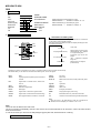
MD-X5H
CP-X5H
MD-X5H and CP-X5H constitute MD-X5H.
• In the interests of user-safety the set should be restored to its original
condition and only parts identical to those specified should be used.
US and foreign patents licensed from Dolby Laboratories Licensing
Corporation.
• Note for users in UK
Recording and playback of any material may require consent
which SHARP is unable to give. Please refer particularly to the
provisions of Copyright Act 1956, the Dramatic and Musical
Performers Protection Act 1956, the Perfmers Protection Acts
1963 and 1972 and to any subsequent statutory enactments and
orders.
CONTENTS
Page
SAFETY PRECAUTION FOR SERVICE MANUAL ........................................................................................................... 2
IMPOTANT SERVICE NOTES (FOR UK ONLY) ............................................................................................................... 3
SPECIFICATIONS ............................................................................................................................................................. 3
NAMES OF PARTS ........................................................................................................................................................... 4
OPERATION MANUAL ...................................................................................................................................................... 6
DISASSEMBLY .................................................................................................................................................................. 8
REMOVING AND REINSTALLING THE MAIN PARTS ................................................................................................... 11
ADJUSTMENT ................................................................................................................................................................. 14
NOTES ON SCHEMATIC DIAGRAM .............................................................................................................................. 35
TYPE OF TRANSISTOR AND LED ................................................................................................................................. 35
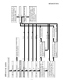
BLOCK DIAGRAM ........................................................................................................................................................... 36
SCHEMATIC DIAGRAM/WIRING SIDE OF P.W.BOARD ............................................................................................... 40
VOLTAGE ........................................................................................................................................................................ 65
WAVEFORMS OF CD CIRCUIT (CD SECTION) ............................................................................................................ 66
WAVEFORMS OF CD CIRCUIT (MD SECTION) ............................................................................................................ 67
TROUBLESHOOTING (CD SECTION) ........................................................................................................................... 69
TROUBLESHOOTING (MD SECTION) ........................................................................................................................... 73
FUNCTION TABLE OF IC ................................................................................................................................................ 78
REPLACEMENT PARTS LIST/EXPLODED VIEW/PACKING PARTS
SHARP CORPORATION
–1–
This document has been published to be used
for after sales service only.
The contents are subject to change without notice.
MD-X5H/CP-X5H
SAFETY PRECAUTION FOR SERVICE MANUAL
WARNINGS (CD)
WARNINGS (MD)
THE AEL (ACCESSIBLE EMISSION LEVEL) OF THE LASER
POWER OUTPUT IS LESS THAN CLASS 1 BUT THE LASER
COMPONENT IS CAPABLE OF EMITTING RADIATION
EXCEEDING THE LIMIT FOR CLASS 1. THEREFORE IT IS
IMPORTANT THAT THE FOLLOWING PRECAUTIONS ARE
OBSERVED DURING SERVICING TO PROTECT YOUR EYES
AGAINST EXPOSURE TO THE LASER BEAM.
1-WHEN THE CABINET IS REMOVED, THE POWER IS TURNED
ON WITDOUT A COMPACT DISC IN POSITION AND THE
PICK-UP IS ON THE OUTER EDGE THE LASER WILL LIGHT
FOR SEVERAL SECONDS TO DETECT A DISC. DO NOT
LOOK INTO THE PICK-UP LENS.
2-THE LASER POWER OUTPUT OF THE PICK-UP UNIT AND
REPLACEMENT SERVICE PARTS ARE ALL FACTORY PRESET BEFORE SHIPMENT.
DO NOT ATTEMPT TO RE-ADJUST THE LASER PICK-UP
UNIT DURING REPLACEMENT OR SERVICING.
3-UNDER NO CIRCUMSTANCES STARE INTO THE PICK-UP
LENS AT ANY TIME.
4-CAUTION-USE OF CONTROLS OR ADJUSTMENTS, OR
PERFORMANCE OF PROCEDURES OTHER THAN THOSE
SPECIFIED HEREIN MAY RESULT IN HAZARDOUS
RADIATION EXPOSURE.
The AEL (ACCESSIBLE EMMISSION LEVEL) of the laser power
output is less than class 1 but the laser component is capable
of emitting radiation exceeding the limit for class 1. Therefore it is
important that the following precautions are observer during
servicing to protect your eyes against exposure to the laser beam.
1) When the unit case cover is removed and LOADING SW (SW
1956) is turned on and then PLAY SW (SW 1954 mechanism
PWB) is turned on in a few second.
The laser will light for several second to detect a disk.
2) The laser power output of the pickup unit and replacement
service parts are all factory pre-set before shipment.
Do not attempt to re-adjust the laser pick-up unit during
replacement or servicing.
3) Under no circumstances stare into the pickup lens at any time.
4) If laser optical unit becomes faulty, replace the complete laser
optical unit.
5) CAUTION-USE of controls or adjustments, or performance of
procedures other than those specified herein may result in
hazardous radiation exposure.
CAUTION - INVISIBLE LASER RADIATION WHEN OPEN AND INTERLOCKS
DEFEATED . AVOID EXPOSURE TO BEAM .
VARNING - OSYNLIG LASERSTRALNING NAR DENNA DEL AR OPPNAD OCH
SPARRAR AR URKOPPLADE . STRALEN AR FARLIG.
ADVARSEL - USYNLIG LASERSTRALING NAR DEKSEL APNES OG SIKKERHEDSLAS
BRYTES . UNNGA EKSPONERING FOR STRALEN .
VARO! AVATTAESSA JA SUOJALUKITUS OHITETTAESSA OLET ALTTIINA
NAKYMATON LASERSATEILYLLE . ALA KATSO SATEESEN .
VARNING - OSYNLIG LASERSTRALING NAR DENNA DEL AR OPPNAD OCH SPARREN
AR URKOPPLAD . BETRAKTA EJ STRALEN .
ADVARSEL - USYNLIG LASERSTRALING VED ABNING . NAR SIKKERHEDSAFBRYDERE
ER UDE AF FUNKTION . UNDGA UDSETTELSE FOR STRALING .
LASER KLASSE 1
LUOKAN 1 LASERLAITE
KLASS 1 LASERAPPARAT
VAROITUS! LAITTEEN KÄYTTÄMINEN MUULLA KUIN TÄSSÄÅ
KÄYTTÖOHJEESSA MAINITULLA TAVALLA SAATTAA
ALTISTAA KÄYTTÄJÄN TURVALLISUUSLUOKAN 1 YLITTÄVÄLLE
NÄKYMÄTTÖMÄLLE LASERSÄTEILYLLE.
CAUTION-INVISIBLE LASER RADIATION WHEN OPEN. DO NOT STARE INTO
BEAM OR VIEW DIRECTLY WITH OPTICAL INSTRUMENTS.
VARNING-OSYNLIG LASERSTRALNING NAR DENNA DEL AR OPPNAD. STIRRA
EJ IN I STRALEN OCH BETRAKTA EJ STRALEN MED OPTISKA INSTRUMENT.
VARNING - OM APPARATEN ANVÄNDS PÅ ANNAT SÄTT ÄN
I DENNA BRUKSANVISNING SPECIFICERAS. KAN
ANVÄNDAREN UTSÄTTAS FÖR OSYNLIG LASERSTRÅLNING,
SOM ÖVERSKRIDER GRÄNSEN FÖR LASERKLASS 1.
ADVERSEL-USYNLIG LASERSTRALING VED ABNING. SE IKKE IND I
STRALEN-HELLER IKKE MED OPTISKE INSTRUMENTER.
VARO! AVATTAESSA OLET ALTTIINA NAKYMATON LASERSATEILYLLE.
ALA TUIJOTA SATEESEEN ALAKA KATSO SITA OPTISEN LAITTEEN LAPI.
VARNING-OSYNLIG LASERSTRALNING NAR DENNA DEL AR OPPNAD.
STIRRA EJ IN I STRALEN OCH BETRAKTA EJ STRALEN GENOM OPTISKT
INSTRUMENT.
ADVERSEL-USYNLIG LASERSTRALING NAR DEKSEL APNES. STIRR IKKE
INN I STRALEN ELLER SE DIREKTE MED OPTISKE INSTRUMENTER.
VARO !Avattaessa ja suojalukitus ohitettaessa olet alttiina näkymättömälle lasersäteilylle. Älä katso säteeseen.
VARNING!
Osynlig laserstralning när denna del är öppnad och spärren är urkopplad. Betrakta ej strälen.
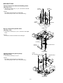
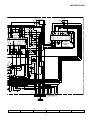
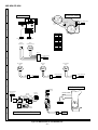
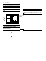
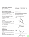
Magnetic Head
Precaution to be taken when replacing and servicing the laser
pickup.
The following precautions must be observed during servicing to
protect your eyesvagainst exposure to the laser.
Warning of possible eye damage when repairing:
If the AC power plug is connected when the inner cover of the unit
is removed, the laser will light up during focus
access (about 1 second) (Fig. 2-1).
During this operation, the laser will leak from the opening between
the magnetic head and cartridge holder (Fig. 2-2).
In order to protect your eyes, you must not look at the laser during
repair.
Before repairing, be sure to disconnect the AC power plug.
Optical pickup
Figure 2-1
Magnet Head
Laser Beam
Cartridge Holder
Mechanism
Chassis
Spindle Motor
Optical pickup
Figure 2-2
–2–
MD-X5H/CP-X5H
FOR A COMPLETE DESCRIPTION OF THE OPERATION OF THIS UNIT, PLEASE REFER
TO THE OPERATION MANUAL.
IMPORTANT SERVICE NOTES ( FOR UK ONLY)
Before returning the unit to the customer after completion of a
repair or adjustment it is necessary for the following withstand
voltage test to be applied to ensure the unit is safe for the
customer to use.
Setting of Withstanding Voltage Tester and set.
Set name
WITHSTANDING
VOLTAGE TESTER
PROBE
+
AC
OUT
set value
-
Withstanding Voltage Tester
Test voltage
4,240 VPEAK
3,000 VRMS
Set time
6 secs
Set current(Cutoff current)
4 mA
SHORT-CIRCUIT
AC POWER
SUPPLY CORD
UNIT
CONNECT THE PROBE
TO GND TERMINAL
OF CHASSIS
OF
PHONO TERMINAL
SCREW
Unit
Judgment
OK: The “GOOD” lamp lights.
NG: The “NG” lamp lights and the buzzor sounds.
SPECIFICATIONS
MD-X5H
Main unit section
(Tuner section)
Frequency range:
(MiniDisc recorder section)
Type:
Signal readout:
Audio channel:
Frequency response:
Rotational speed:
Quantization:
Filter:
Error correction:
Coding:
Recording Method:
D/A converter:
Sampling frequency:
Wow and flutter:
Signal/noise ratio:
Dynamic range:
T.H.D at 1 kHz:
Sensitivity:
MiniDisc recorder
Non-contact, 3-beam semi-conductor
laser pick-up
Stereo; 2 channel
Monaural; 1 channel (long-time
recording mode)
20 - 20,000 Hz
400 - 900 rpm CLV, Approx.
16-bit linear
8-times oversampling digital filter
ACIRC (Advanced Cross Interleave
Reed-solomon Code)
ATRAC (Adaptive Tranceformed
Acoustic Coding)
Magnetic modulation overwrite method
1-bit
44.1 kHz
Unmeasurable
(less than 0.001% W. peak)
95 dB (1kHz)
90 dB (1kHz)
0.1%
(General)
Power source:
Power consumption:
Output power:
Input terminals:
Output terminals:
Dimensions:
Weight:
Rotational speed:
Error correction:
Quantization:
D/A converter:
Filter:
Frequency response:
Signal/noise ratio:
Dynamic range:
Wow and flutter:
AC 230 V, 50 Hz
80 W
PMPO; 80 W (total)
MPO; 40 W (20 W+20 W) DIN 45 324
RMS; 25 W(12.5 W+ 12.5 W) DIN 45 324
Auxilialy (Analog); 2.0 V (30 kohms)
Auxilialy (Digital-1)
Auxilialy (Digital-2)
Phono; 2.5 mV (10 kohm)
Headphones; 16-50 ohms
(recommended; 32 ohms)
Speakers; 6 ohms
Line out (Analog); 2.0 V (47 kohm)
Width; 150 mm (5-15/16")
Height; 241 mm (9-1/2")
Depth; 307 mm (12-1/8")
4.3 kg (9.5 lbs.)
CP-X5H
(Compact disc player)
Type:
Signal readout:
FM; 87.5 - 108 MHz
AM; 522 - 1,620 kHz
FM; 8.0 µV (75 ohms, unbalanced)
AM; 650 µV/m
Speaker section
Compact disc player
Non-contact, 3-beam semi-conductor
laser pickup
200 - 500 rpm CLV, Approx.
CIRC (Cross Interleave ReedSolomon Code)
16-bit linear
1-bit
4-times oversampling digital filter
20 - 20,000 Hz
95 dB (1 kHz)
90 dB (1 kHz)
Unmeasurable
(less than 0.001% W. peak)
Type:
2-way 120 mm (4-3/4") woofer and
50 mm (2") tweeter type
Maximum input power: 25 W
Rated input power:
12.5 W
Impedance:
6 ohms
Dimensions:
Width; 146 mm (5-3/4")
Height; 241 mm (9-1/2")
Depth; 229 mm (9-1/8")
Weight:
2.2 kg (4.9 lbs. )/each
Specifications for this model are subject to change without
prior notice.
–3–
MD-X5H/CP-X5H
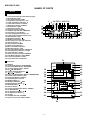
NAMES OF PARTS
MD-X5H
Display window
1. Level meter/Character Information Display
2. EON Indicator: EON
3. Disc Name Indicator: DISC
4. Programme Type Indicator: PTY
5. Traffic Information Indicator: TI
6. Track Name Indicator: TRACK
7. FM Stereo Indicator: STEREO
8. Data Indicator: DATE
9. FM Stereo Indicator: ST
10. Program Indicator: PRGM
11. Random Play Indicator: RANDOM
12. Recording Level Indicator
13. Traffic Programme Indicator: TP
14. Traffic Announcement Indicator: TA
15. RDS Indicator: RDS
16. MD Pause Indicator:
17. MD Record Indicator: REC
18. Recording Level Too High Indicator
19. Repeat Indicator:
20. Sleep Indicator: SLEEP
21. More Tracks Indicator: >
22. Music Schedule Indicators
23. MD TOC Indicator: TOC
24. Recording Mode Indicator: MONO LP
25. Sound Synchro Indicator: S. SYNC
26. Clock Indicator: CLOCK
27. Remaining Time Indicator: REMAIN
28. Auto Mark Indicator: AUTO MARK
29. Total Time Indicator: TOTAL
30. Timer/Timer Record Indicator
1 2 3 4 5 678 910 1112
13
14
15
18
19
16
17
20
21
22 23
24 252627 28 29 30
31
Front panel
MD/CD COMPONENT SYSTEM MD-X5
31. MD Slot
32. On/Stand-by Button: ON/STAND-BY
33. Recording Mode Button: REC MODE
34. CD Track Select Button: TRACK
35. CD MD Edit Button
36. Volume Up/Down Buttons:
37.
.-/+ Buttons
38. Tuner Call (Band Select) Button: TUNER(BAND)
39. Auxiliary Select Button: AUX
40. Extra Bass Button: X-BASS
41. Keyboard Input Terminal
42. MD Eject Button:
43. MD Record Button: REC
44. MD Play/Pause Button:
45. MD Stop Button:
46. Remote Sensor
47. Pre-program Equalizer Button: PRE-EQ
48. CD Stop Button:
49. CD Play/Pause Button:
50. CD Open/Close Button:
51. CD Tray
52. Headphoned Jack: PHONES
53. Input Level Control: INPUT LEVEL
REC
32
33
34
35
ON/STAND-BY
EDIT
REC MODE
TRACK
CD MD
REMOTE
SENSOR
42
43
44
45
46
SAMPLING RATE CONVERTER
36
37
EON
47
48
49
50
VOLUME
MD/CD/TUNER
PRE-EQ
38
39
40
TUNER(BAND)
AUX
51
KEYBOARD INPUTLEVEL
41
PHONES
52
5 V ... MAX 300 mA
53
–4–
X-BASS
MD-X5H/CP-X5H
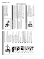
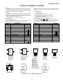
MD-X5H
Rear Panel
ANTENNA
1
2
1. AM Loop Aerial Input Socket
2. FM 75 ohms Aerial Socket
3. Phono Input Sockets
4. Auxiliary Analog Input Jacks
5. Auxiliary Analog Output Jacks
6. Auxiliary Digital Input Jack (Optical)
7. Auxiliary Digital Input Jack (Coaxial)
8. AC Power Cord
9. Reset Button
10. Speaker Terminals
AM
LOOP
FM
75 OHMS
PHONO
3
4
5
6
7
RIGHT
GND
LEFT
AUX ANALOG IN/OUT
AUX
IN
RESET
AUX
OUT
RIGHT
LEFT
9
RATED SPEAKER
IMPEDANCE ;
6 OHMS MIN.
DIGITAL1
OPTICAL
LEFT
DIGITAL2
COAXIAL
RIGHT
10
AUX
DIGITAL
IN
SPEAKERS
8
CP-X5H
1
Speaker section
1. Tweeter
2. Woofer
3. Speaker cord
2
MD-X5H
3
Remote Control
1. MD Track Up/Down, Cue/Review Buttons:
2. Tuner Preset CD/MDTack Number InputButtons
3. Program Button: PROGRAM
4. Clear Button: CLEAR
5. MD Record Button: REC
6. Play Mode Button: P-MODE
7. Time Display Select Button: TIME
8. Auxiliary Select Button: AUX
9. Cursor Buttons: CURSOR
10. Name/TOC Edit Button: NAME/TOC EDIT
11. Timer/Delete Button: TIMER/DELETE
12. On/Stand-by Button: ON/STAND-BY
13. Extra Bass Button: X-BASS
14. Tuning Up/Down Buttons:
15. Programme Type/Traffic Information Search Button:
PTY TI
16. EON Button: EON
17. ASPM Button: ASPM
18. FM Stereo Mode Button: ST-MODE
19. Tuner Call (Band Select) Button: TUNER/BAND
20. MD Stop Button:
21. MD Play/Pause Button:
22. Sound Synchro Button: S. SYNC
23. Recording Mode Button: REC MODE
24. Auto Mark Button: A.MARK
25. CD Play/Pause Button:
26. CD Stop Button:
27. CD Track Up/Down, Cue/Review Buttons:
28. Display Button: DISPLAY
29.
Buttons
30. Message Button: MESSAGE
31. Enter Button: ENTER
32. Volume Up/Down Buttons:
33. Pre-programme Equalizer Button: PRE-EQ
1
MD/CD/TUNER DIRECT KEY
2
3
4
5
6
1
2
3
4
5
6
7
8
9
10/0
PTY TI
EON
ASPM
ST-MODE
-TUNERBAND
>10
RDS
PROGRAM
TUNING
CLEAR
P-MODE
MD
REC S.SYNC REC MODE A.MARK
TIME
CD
7
8
9
-AUX-
<< CURSOR >>
DISPLAY
27
28
TIMER/
DELETE
MESSAGE
29
30
31
32
11
ON/STAND-BY X-BASS PRO-EQ
VOLUME
12
13
25
26
NAME
TOC EDIT
ENTER
10
14
15
16
17
18
19
20
21
22
23
24
REMOTE CONTROL
MD/CD COMPONENT SYSTEM
33
–5–
–6–
14
13
12
11
10
9
8
7
6
5
4
3
2
ON/STAND-BY
TIMER/
DELETE
ENTER
or
button to select "TIME ADJUST".
Within 10 seconds, press the ENTER button.
The unit will enter the date setting mode.
Within 10 seconds, press the
Press the TIMER/DELETE button.
Press the ON/STAND-BY button to turn the power on.
Press the TIMER/DELETE button, and press the or button until the
date and time appear.
I When about 10 seconds have elapsed, the original display will reappear.
To check the date and time:
If you don't need to change the settings, just press the ENTER button.
Once you have set the date and time, "TIME ADJUST" will not be
displayed in step 3. Press the or button to make the date and time
appear.
To change the setting:
Notes:
In the event of a power failure or when the AC power lead is disconnected, the clock display will go out.
When the AC power supply is restored, the clock display will flash on
and off to indicate the time when the power failure occurred or when the
AC power lead was disconnected.
Whilst recording an MD, you cannot set the date and clock. Be sure to
set the date and clock before recording.
The range of dates that can be entered is from January 1, 1997 to
December 31, 2049.
The clock will start operating.
When about 3 seconds have elapsed, the original display will reappear.
14 Press the ENTER button to set the minute.
button.
Press the button once to increase or decrease the minutes by one.
When the button is held down, the time will change in increments of 5
minutes.
12 Press the ENTER button to set the hour.
13 Adjust the minute by pressing the or
or
button.
Press the button once to increase or decrease the hour by one. Keep
pressing it to advance continuously.
11 Adjust the hour by pressing the
The unit will enter the time setting mode.
10 Press the ENTER button to set the year.
Press the button once to increase or decrease the year by one. Keep
pressing it to advance continuously.
For a year after 2000, set "00" for 2000, "01" for 2001 and so on.
5 Adjust the day by pressing the or button.
6 Press the ENTER button to set the date.
7 Adjust the month by pressing the or button.
8 Press the ENTER button to set the month.
9 Adjust the year by pressing the or button.
1
2
3
4
When you have set the date and time, this unit can be used as a clock. It
can be used for timer recording or for timer playback. It is also used to store
the MD recording date in memory.
15
(8" - 20')
0.2m - 6m
For MiniDiscs which repeated recording and editing operations were performed,
the COMBINE function may not work.
Two tracks may not be combined in editing.
TROUBLESHOOTING
RESET
1
2
3
When the RESET button is pressed, all of the settings in memory will be
erased.
If strange sounds, smells or smoke come out of the unit, or if a foreign
object falls into the unit, turn off the power, unplug the AC power lead
from the AC socket immediately. Contact the shop where you purchased the unit.
Plug the AC power lead back into the AC socket.
Press the RESET button on the back of the unit for at least 3 seconds.
Unplug the AC power lead from the AC socket.
If this product is subjected to strong external interference (mechanical
shock, excessive static electricity, abnormal supply voltage due to lightning, etc.) or if it is operated incorrectly, it may malfunction or the display
may not function correctly. If such a problem occurs, do the following:
If a problem occurs
A cluster (about 2 seconds) is normally the minimum unit of recording. So, even if a
track is less than 2 seconds long, it will use about 2 seconds of space on the disc.
Therefore, the time actually available for recording may be less than the remaining
time displayed.
If there are scratches on a disc, those sections will be automatically avoided (no
recording will be placed in those sections). Therefore, recording time will be
reduced.
When the remaining recording time of a disc is displayed, short tracks less than 15
seconds long may not be included in the total.
Even if several short tracks are erased, the remaining
recording time may not show an increase.
The total of the recorded time and time remaining on a disc
may not add up to the maximum possible recording time.
When emphasis information (equalizer treatment in the treble section) in a track
switches on/off many times, each change is assumed to be the beginning of a new
track, which will quickly use up all available track numbers, making further recording
impossible, regardless of the remaining time, recording time or the number of tracks
on the original.
When the number of tracks used reaches the limit, regardless of the remainder being
recording time, further recording will be impossible. (Maximum number of tracks: 255)
Replace the batteries if the control distance decreases or operation
becomes erratic.
Periodically clean the transmitter LED on the remote control and the
sensor on the main unit with a soft cloth.
Exposing the sensor on the main unit to strong light may interfere with
operation. Change the lighting or the direction of the unit.
Keep the remote control away from moisture, excessive heat, shock,
and vibrations.
Notes concerning use:
Even if the number of tracks and the recording time have
not reached the limit, “DISC FULL” may be displayed.
Even if the maximum recording time of a MiniDisc is not
reached, “DISC FULL” or “TOC FULL” may be displayed.
MINIDISC SYSTEM LIMITATIONS
Remote sensor
PREPARATION FOR USE
15
SETTING THE CLOCK
MD-X5H/CP-X5H
OPERATION MANUAL
BLANK MD
• Recording cannot be performed correctly due to vibration
Can't REC
• The disc is out of recording space.
• There is no space left for recording CD.
• The proper focus cannot be obtained.
• The unit has determined that it is out of order
DISC FULL
EDIT OVER
FOCUS ERROR
MD ERROR
–7–
• The unit has determined that it is out of order by performing a
PROTECT
• The temperature is too high.
• The disc has a large amount of damage.
TEMP OVER
TOC ERR*
specifications or it cannot be read.
• The TOC information on this disc does not meet the MD
• Music is not recorded.
0 00:00
*: Number or symbol
• The data contains an error.
? DISC
a mechanical shock or to scratches on the disc.
U TOC W ERROR • The TOC information could not be created properly due to
U TOC ERR*
by performing a self-diagnosis.
• The unit has determined that it is abnormal
(track names, disc names, etc.).
• There is no space left for recording character information
• The MD does not meet the specifications for MDs.
• TOC information cannot be read.
• The disc is write protected.
PROTECTED
self-diagnosis.
• You tried to record on a playback-only disc.
button.
• Replace the disc with a recorded disc.
• Replace the disc with another disc.
(Remove any source of shock or vibration whilst writing.)
• Turn off the power, and try to write the TOC again.
• Erase all the data, and try recording.
• Replace it with another disc.
• Ask the store where you purchased this unit, about repairs.
• Replace it with another recordable disc.
• Replace the disc with another disc.
• Turn off the power, and wait for a while.
• Move the write protection tab back to its original position.
ask the store where you purchased this unit, about repairs.
• Turn the power off and back on. If the problem is not resolved,
• Replace it with a recordable disc.
• Replace the disc.
• Select another track.
• Reload the disc.
• Shorten the disc or track name.
• Turn off the power, and press the
• Ask the store where you purchased this unit, about repairs.
• Reload the disc.
• Replace it with another recordable disc.
• Replace the disc with another recordable disc.
• Reload the disc or replace it.
• Use analogue inputs.
• Connect correct digital signals.
• Replace the disc with another recordable disc.
• Rerecord or replace it.
• Load a disc.
PLAYBACK MD
TOC W ERROR
• Replace it with another disc which you can copy from (regular CD).
• Change the stop position of the track and then try editing it.
• The disc data cannot be read.
• The data recorded on this disc is not audio data.
TOC FULL*
Remedy
• Replace the disc with a recorded disc.
• A disc has not been loaded.
exceeds 100.
• The number of characters for the disc name or track name
NOT AUDIO
NO DISC
NAME FULL
properly.
• There is a mechanical problem and the disc is not working
by performing a self-diagnosis.
• The disc is damaged or there is no TOC on the disc.
DISC ERR*
MECHA ERR*
• Incorrect digital signals are input.
was skipped.
• Since this disc has scratches on it, the recording operation
Din UNLOCK
DEFECT
• A track cannot be edited.
Can't EDIT
or shock in the unit.
• You tried to record from a disc which you are not allowed to copy.
Can't COPY
(Neither music nor a disc name have been recorded on this MD.)
Meaning
• Nothing is recorded.
Error messages
When an error message is displayed, proceed as follows:
(Continued)
MD-X5H/CP-X5H
MD-X5H/CP-X5H
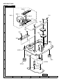
DISASSEMBLY
Caution on Disassembly
Whe disassembling the machine or assenbling it after
repair, observe the following instructions so as to ensure
safety and keep its performance.
1. Unload the compact disc, and mini-disc from machine.
2. Be sure to unplug the power cable before starting
disasembly of the machine.
3. When disassenbling each section, remove the nylon
band or wire arrangement.
If a screw of improper length is fit to the MD mechanism.
(a screw fit the part to the mechanism chassis of MD
section), it may cantact the optical pickup, impeding
normal operation. Hence, due care must be taken.
4. While repairing, pay utmost attention to static electricity
on ICs.
REMOVAL
(A1)x1
ø3x10mm
(B1)x1 Top Cabinet
ø3x10mm
(B1)x1
ø3x10mm
Side Panel
(Right)
(A1)x2
ø3x10mm
PROCEDURE
FIGURE
1
Top Cabinet
1. Screw ................ (A1) x4
8-1
2
Side Panel
(Left/Right)
1. Screw ................ (B1) x10
8-1
3
Rear Panel
1. Screw ................ (C1) x6
2. Socket ............... (C2) x1
8-1
8-2
4
Power Amp. PWB
1. Screw ................ (D1) x2
2. Socket ............... (D2) x4
8-2
5
Main PWB
1. Screw ................ (E1) x2
2. Socket ............... (E2) x4
3. Flat Wire ............ (E3) x1
8-2
8-3
6
MD Holder
(MD Unit)
1. Screw ................ (F1) x4
2. Socket ............... (F2) x1
3. Flat Cable .......... (F3) x1
8-3
7
Power Supply PWB 1. Screw ................ (G1) x4
8-3
8
CD Holder
(CD Mechanism/
CD Servo PWB)
9-1
(B1)x2
ø3x10mm
(B1)x2
ø3x10mm
(B1)x2
ø3x10mm
Rear Panel
Side Panel
(Left)
1. Screw ................ (H1) x4
2. Socket ............... (H2) x1
3. Flat Wire ............ (H3) x1
(E2)x1
(E1)x1
ø3x10mm
Main PWB
(D2)x1
(C2)x1
(D2)x1
(E3)x1
(E2)x2
9
Front Panel
1. Screw ................ (J1) x2
9-1
Display PWB
1. Screw ................ (K1) x10
9-1
11
Jack PWB
1. Screw ................ (L1) x2
9-2
12
CD Servo PWB
(Note 1)
1. Screw ................ (M1) x3
9-3
13
CD Mechanism
1. Screw ................ (N1) x3
9-4
14
MD Mecha Unit
1. Screw ................ (P1) x7
9-5
15
MD Main PWB
1. Screw ................ (Q1) x4
2. Socket ............... (Q2) x6
9-6
16
MD Mechanism
1. Screw ................ (R1) x4
10-1
(E2)x1
(E1)x1
ø3x10mm
(D1)x1
ø3x10mm
(D2)x1
Pull
Pull
Power Amp. PWB
(D1)x1
ø3x10mm
Figure 8-2
MD Mecha Unit
(F1)x2
ø2.6x10mm
CP-X5H
REMOVAL
(B1)x1
ø3x10mm
Figure 8-1
10
STEP
(A1)x1
ø3x10mm
(B1)x2
ø3x10mm
(C1)x6
ø3x8mm
MD-X5H
STEP
MD-X5H
PROCEDURE
FIGURE
1
Front Panel
1. Net ........................... (A1) x2 10-2~5
3. Screw ...................... (A2) x6
2
Speaker
1. Screw ...................... (B1) x4
10-6
3
Tweeter
1. Screw ...................... (C1) x2
10-6
MD Holder
(F1)x2
ø2.6x10mm
(D2)x1
(G1)x4
ø4x10mm
Note 1: After disconnecting the optical pickup connector wrap
the front end of connector in the conductive aluminium foil so
as to prevent electrostatic damage of optical pickup.
(F2)x1
(F3)x1
Power Supply PWB
Figure 8-3
–8–
MD-X5H/CP-X5H
Shield Case (Top Sode)
Front Panel
(P1) x 1
ø2 x 4mm
(K1)x10
ø2.6x10mm
(P1) x 1
ø2 x 4mm
Display PWB
(H1)x4
ø3x10mm
(H3)x1
MDMecha Unit
(H2)x1
(P1) x 1
ø2 x 4mm
CD Holder
(J1)x2
ø3x6mm
Figure 9-1
Shield Case
(Bottom Side)
(P1) x 1
ø2 x 4mm
(P 1) x 1
ø3 x 10mm
(P1) x2
ø3 x 10mm
Front Panel
Figure 9-5
Jack PWB
( Q2 ) x 1
(L1)x2
ø2.6x10mm
Pickup Flexible
PWB (*1)
Figure 9-2
MD Main PWB
( Q1 ) x 4
ø1.7 x 3mm
Pull
(M1)x3
ø2.6x10mm
(Q2)x1
(*1) After disconnecting the optical
pickup flex PWB from the
connector wrap the front end of
flex PWB in conductive aluminium
foil so as to prevent electrostatic
damage of optical pickup.
CD Servo PWB
( Q2 ) x 1
( Q2 ) x 3
Figure 9-3
(N1)x3
ø2.6x10mm
Frame
Figure 9-6
CD Mechanism
Figure 9-4
–9–
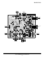
MD-X5H/CP-X5H
4
MD Mechanism
Push the vicinity of end
of center decoration notch.
Insert the head of screwdriver near 4 , push further the
screwdriver, pulling up the net. Thereby the lower pawl is
disengaged (at first disengage at one side and then at other
side).
6 After disengaging both pawls disengage the upper pawl by
the same procedure as stated in 3 above.
Figure 10-4
5
(R1)x4
ø1.7x8.9mm
Figure 10-1
CP-X5H
1
(A2)x4
ø4x16mm
Bottom Side
Insert the head of screwdriver
or metallic bar (2.5 or less) into
the panel notch hole.
(A1)x2
Figure 10-2
Front Pane
(A2)x2
ø4x16mm
2 Insert the head of screwdriver into the hole,
and push further the screwdriver, pulling up
the net. Thereby the lower pawl is disengaged
Figure 10-5
It is better to hold the
screwdriver aslant as
shown in the figure.
3 After disengaging the
1 lower pawl pull slightly
in the arrow direction 1 , and then pull in the
direction 2 . Thereby the net can be removed.
Tweeter
1
2
(C1)x2
ø4x16mm
(B1)x4
ø4x16mm
Speaker
Figure 10-3
Figure 10-6
– 10 –
MD-X5H/CP-X5H
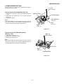
REMOVING AND REINSTALLING THE MAIN PARTS
(A1)x1
ø1.7x5mm
MD MECHANISM SECTION
Perform steps 1 to 3 of the disassembly method to remove the
MD mechanism.
How to remove the magnetic head
(See Fig. 11-1)
Magnetic Head
1. Remove the screws (A1) x 1 pc.
Caution:
Take utmost care so that the magnetic head is not damaged
when it is mounted.
MD Mechanism
Figure 11-1
Slider Lever
How to remove the cartridge holder
(See Fig. 11-2)
Cartridge Holder
Roller Arm Lever
1. Open the rpller arm lever in the arrow direction, and lower
the clamper lever to the rear side.
2. Apply +5V to the red line side of blue connector of loading
motor, push the rack gear in the arrow direction to move the
cam plate lever until tick is heard.
3. Remove the screw (B1) x1 pc., and the spring (B2) x1 pc.,
fitted to the holder arm, and shift the cartridge holder to the
left side to remove it.
Clampa Lever
(B1) x1
Ø1.7x5mm
Loading Motor
Lack Gear
Cam Plate Lever
(B2) x1
Figure 11-2
(C1)x1
Ø1.7x3mm
How to remove the mechanism switch PWB
(See Fig. 11-3)
1. Remove the screws (C1) x 2 pcs., and remove the mechanism
switch PWB.
(C1)x1
Ø1.7x9.5mm
MD Mechanism
Switch PWB
Figure 11-3
– 11 –
MD-X5H/CP-X5H
How to remove the sled motor/loading motor
(See Fig. 12-1)
1. Remove the screws (D1) x 1 pcs., and remove the sled
motor/loading motor.
(D1)x2
Ø1.7x2mm
(D1)x2
Ø1.7x2mm
Caution:
Be careful so that the gear is not damaged.
(The damaged gear emits noise during searching.)
Loading
Motor
Sled Motor
Figure 12-1
How to remove the spindle motor
(See Fig. 12-2)
1. Remove the screws (E1) x 3 pcs., and remove the spidle
motor.
Caution:
Be careful so that the turntable is not damaged.
Turntable
(E1)x3
Ø1.7x2.5mm
Spindle Motor
Figure 12-2
(F1)x3
Ø1.7x9.5mm
How to remove the optical pickup
(See Fig. 12-3)
Optical Pickup
1. Remove the screws (F1) x 3 pcs.
Caution:
Be careful so that the gear is not damaged.
(The damaged gear emits noise during searching.)
Figure 12-3
– 12 –
MD-X5H/CP-X5H
CD MECHANISM SECTION
Perform steps 1,to 7 and 12 of the disassembly method to
remove the CD mechanism.
( A1 ) x2
2.6 x 6 mm
How to remove the pickup (See Fig. 13-1)
Optical Pickup
1. Remove the screw (A1) x 2 pcs., to remove the shaft (A2)
x 1 pc.
2. Remove the stop washer (A3) x 1 pc., to remove the gear
(A4) x1 pc.
3. Remove the pickup.
CD Mechanism
Stop Wassher
( A3 ) x1
Note:
After disconnecting the optical pickup connector wrap the
front end of connector in the conductive aluminium foil so as
to prevent electrostatic damage of optical pickup.
Gear
( A4 ) x1
Shaft
( A2 ) x1
Figure 13-1
How to remove the CD loading motor
(See Fig. 13-2)
(B2) x 2
Ø 2 x 4mm
1. Remove the belt (B1) x 1 pc.
2. Remove the screw (B2) x 2 pcs.
3. Remove the loading motor.
Note:
After disconnecting the optical pickup connector wrap the
front end of connector in the conductive aluminium foil so as
to prevent electrostatic damage of optical pickup.
CD Unit
Belt
(B1) x 1
Loading Motor
Figure 13-2
– 13 –
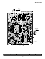
MD-X5H/CP-X5H
ADJUSTMENT
TUNER SECTION
• Setting the Test Mode
Holding down the PRE-EQ button and TUNER(BAND) button,
press the POWER button. Frequency is set in the memory as
shown in Table 19. Call it with the PRESET button for tuner
circuit adjustment and check.
fL: Low-range frequency
fH: High-renge frequency
• AM IF/RF
AM Signal oscillator Frequency 400 Hz, 30% modulation
Adjusting item
Adjusting object
Adjusting
method
IF
T351 Indication of
IF waveform 450
set must be 1,620 kHz. kHz is set to max.
Frequency cover
(Voltage of Pin 20
IC302 VT line)
fL: T302 (522 kHz)
Set Diplay of 522 kHz.
fL: 1.1 ± 0.1 V
fH: 5.1 ± 1.3 V of
(Only check)
Tracking
fL: T302 (990 kHz)
Set output of
speaker terminal
to maximum.
Frequency
Preset No.
P01
P02
P03
P04
P05
87.5 MHz
108.0 MHz
90.0 MHz
106.0 MHz
98.0 MHz
Preset No.
P06
P07
P08
P09
P10
Frequency
522 kHz
1,620 kHz
603 kHz
1,404 kHz
990 kHz
• FM Mute Level
FM Signal oscillator Frequency 400 Hz, 22.5 kHz
Adjusting
method
Adjusting
method
Adjusting
object
98.0 MHz
(30 dB)
98.0 MHz
VR351
Adjusting object
Input: SO301
Output: Speaker
Terminal
AM Loop Antenna
Electric
Voltmeter
IF: Speaker Terminal
Frequency cover: IC302 Pin20
Speaker
terminal
SO301
FM signal oscillator
AM signal oscillator
UNIT
UNIT
GND
Loop Antenna
Figure 14-2 FM Mute Level
Figure 14-1 AM IF
AM
TRACKING fL
ANTENNA
TERMINAL
AM BAND
COVERAGE fL
T302
VR351
FE301
20
13
IC302
1
T351
FM MUTE
LEVEL
12
MAIN PWB
Figure 14-3 ADJUSTMENT POINTS
– 14 –
AM IF
Electric
Voltmeter
MD-X5H/CP-X5H
CD TEST MODE
CD test mode setting
Any TEST mode can be set as shown below by pressing several buttons.
Holding down TACK UP/CUE and CD PLAY/PAUSE, turn on POWER.
Test Mode
Function - CD TEST mode
Test mode setting
Initialization is not executed.
CD TEST mode indication
button.
Open/Close operation is
The pickup can be moved with the (
) or (
) button.
<TRACK>
On-spot tracking
Servo OFF playback
<CD>MD EDIT>
On-spot tracking
Servo ON playback
<PLAY> button input - TOC. Initialization is executed, and normal PLAY is executed.
Press the <STOP> button.
Stop
If the following button is pressed during PLAY, any track No. can be specified directly.
<TUNER (BAND)> button: Track 4
<AUX> button: Track 9
<X-BASS> button: Track 15
Note:
) or (
) button only in STOP state.
The pickup can be moved with the (
Cancel method: POWER OFF
CD section
The CD system has the following automatic adjusting function. Therefore readjustment is not required when the pickup is
replaced. Since adjustment of this CD unit is not required, the combination of PWB and laser pickup unit is not restricted.
Automatic adjustment items
1. Focus Offset (Fig. 15-1)
2. Tracking Offset (Fig. 15-2)
3. E/F Balance (Tracking Error Balance) (Fig. 15-3)
4. R/F level AGC function (HF level: Constant)
5. Tracking gain RF level automatic follow-up
0.1s
This adjustment is executed whenever the disc is
0.50 V
changed. Therefore the optimum setting is used for
IC1 20 FE
playback of each disc.
Focus Offset
Adjustment
0.1s
0.50 V
IC1 7 TE
Tracking Offset
Adjustment
1
2
Figure 15-1
Tracking/
Error Balance
Adjustment
200 ms
1V/diV
IC 1 15
10ms
0.50 V
IC1 20 FE
1
TO
10ms
0.50 V
IC1 7 TE
Tracking
Offset
1 Adjustment
200 ms
1V/diV
IC 1 7
TE
2
2
Figure 15-2
Figure 15-3
– 15 –
MD-X5H/CP-X5H
RDS
1. RDS Function
Function
PI
PS
PTY
PTY(31)
EON TI (TA)
EON-PTY
EON-AF
TP
TA
ASPM
STATION NAME
PTY SEARCH
Select and search (18 kind items) by cyclic
NEWS-AFFAIRS ------ OTHER M - ALARM - TP - TA
STAND-BY MODE
EON-TI/PTY
With EON-AF
ind.
ind.
Select and stand-by (17 kind items) by cyclic
NEWS-AFFAIRS ------ OTHER M - ALARM - TI
2. DISPLAY
DISPLAYand
andcontrol
controlbuttons
buttos
Information Provided by RDS
EON
ASPM
PTY TI
With the MD-X5H, you can watch two types of RDS service. To show them
on the display, press the DISPLAY button.
Each time you press the DISPLAY button, the display will change to show
the following information.
Level meter:
DISPLAY
Level meter
PS (Programme Service):
Station names commonly known
will be displayed. "PS: " appears
if no signal is being sent.
PTY (Programme Type):
Programme type will be displayed.
"PTY: " appears if no signal is
being sent.
ENTER
Station name:
Station name you assigned.
(Preset station)
Descriptions of the PTY (Programme Type) codes, TP (Traffic Programme) and TA (Traffic Announcement)
With the MD-X5H, you can search for and receive the following PTY, TP and TA signals.
News:
News
Pop M:
Pop music
Affairs:
Topical programme expanding on the current news
Rock M:
Rock music
or affairs
M.o.R. M:
Middle-of-the-road music (usually called "easy listen-
Info:
Programmes on medical service, weather fore-
ing")
cast, etc.
Light M:
Light music
Sport:
Sports events
Classics:
Classics
Educate:
Educational programmes
Other M:
Other music
Drama:
Radio plays
Alarm:
Emergency broadcasts
Culture:
Programmes on national or regional culture
NONE:
No programme type (receive only)
Science:
Programmes on national sciences and technology
TP:
Broadcasts which carry traffic announcements
Varied:
Other programmes like comedies or ceremonies
TA:
Traffic announcements are being broadcast at present.
Note:
When the unit is in the EON stand-by mode and a programme is
selected, the unit will display "TI" instead of "TP" or "TA".
Note:
TP and TA ind. are different from CD-C75H.
TP, TA ind. can light up individually, when TP: OFF and TA: ON, it means that EON-TI can be used, in case of TP=OFF, TA=OFF,
EON-Ti can't be used.
In case of CD-C75H, (TP: OFF and TA: ON) disregard (ignore) this case, because EON-TI is nothing.
AF: Alternative
Alternative Frequencycies
AF:
Frequencycies
– 16 –
– 17 –
Yes
Yes
Compare the field strength of current
receiving signal. Is receiving signal
stronger than signal which has same PI
cord and is already memorized to
preset memory ahead of this receiving
time?
Yes
Comparing PI cord same or not?
between current receiving PI and
before PI which is already memorized
by ASPM on this time.
Yes
RDS signal or not? PI—identify
If count 2nd OK?
If count 1st OK?
Yes
SD (TUNE) DET out OK?
Begin to scan start 87.50 → 108.00 MHz
No
Preset CH memory full over?
“ASPM” blinks in the display.
Yes
No
No
No
No
No
No
Yes
Hold down the ASPM button for 3 more second.
ASPM, summary operation
Comparing freg. same or not?
Between current receiving frequency
and (already) previously memorized
frequency.
Yes
Comparing freg. same or not?
between current receiving frequency
and (already) previously memorized
frequency.
Yes
No
No
Effect
No effect
Memorized to the lowest
vacant preset channel.
No effect
No effect
Memorized to the lowest
vacant preset channel.
Pass
No effect
Pass
No effect
Pass
No effect
Pass
No effect
No operate. After displayed “0 MEMORY END”.
Return to previous station.
Repeat and continue with same format
ASPM operation untill 108 MHz.
After reached 108 MHz, displayed the
TTL quantity of memorized stations.
And return to the previous receiving
freq. automatically.
Begin to ASPM SCAN from the next
CH-SPAN again.
No
Preset CH memory become full over?
Yes
Displayed the TTL quantity of memorized stations by ASPM operation on
this time. And return to the previous
receiving freq. automatically.
MD-X5H/CP-X5H
MD-X5H/CP-X5H
• ASPM SCAN: 87.50MHz → 108.00 MHz.
• Only RDS signal is memorized by ASPM because RDS signal has PI code and is suitable and convenient for ASPM operation.
ASPM
Comparing field strength, only one strongest RDS station is memorized of all stations (repeater relay stations) that have same
PI code.
f3
P 1 (PI cord)
PS 1 (Station Name)
f5
P2
PS 2
f4
---
f1
f2
---
Each PI has AF’S list by individually.
Exa: P1 has f1, f2, f3 (same PTY).
Same PI code — freq: different
P2 has f4, f5 (same PTY).
(AF’S)
PS: same
PTY: same
[For example]
Pickup and memorized to preset CH.
f8
f9
f 10
f 11 f 12 f13
f6
f7
P3
PS 3
P4
PS 4
Select signals (f1, f5, f7, f10) are memorized in the preset memory by ASPM.
• If tentative - ASPM operation is repeated intententionally, never memorized (over write) at the same frequecy.
1st time ASPM → strongest stations of each pi are memorized.
ASPM is not only very usefull for PTY search, but also EON operation.
2nd time ASPM → 2nd strong stations of each pi are memorized and so on.
PTY search function is equal to FM band search function as a result.
1. Introduction of RDS for MD-X5H
MD-X5H RDS function is equal to adding EON feature to the current CD-C75H RDS.
EON feature is EON—PTY and EON—TI.
Although PTY and TI indicators are separated, PTY contains TI in the PTY items (software) like current PTY search items.
NEWS,
AFFAIRS,
INFO,
ALARM,
TI
(TTL 17 kinds)
↑
↑
EON—PTY
EON—TI
Can select and stand-by
Can select and stand-by
EON—PTY and EON—TI are basically stand-by → receive the desired program of ON station.
2.The difference point from current CD-C75H RDS. (CD-C75H — MD-X5H)
1. PTY item: added TA.TTL 18 kind.
2. Each “TP”, “TA” ind. light up or go out individually.
“TA” ind. doesn’t light up on current model, CD-C75H due to none EON—TI.
3. Added 3 indicators(in FL) due to adding EON feature.
EON: Lights up only during receiving EON data (14A).
TI:
During EON-TI stand-by → Light up
During receiving ON station. → blink.
PTY: During EON-PTY stanb-by → Light up
During receiving ON station. → blink.
4. No adjust type (None adjusting circuit.)
5. Added EON button.
6. Need to change RDS logo due to add EON feature.
7. Added EON—TI, EON—PTY function.
3. Summary of MD-X5H RDS—EON operation
EON—PTY: Select and set the desired “PTY” → stand-by → switch to ON(other network) Station at the start of desired
PTY automatically → stay and listen to PTY of ON station → switch back to TN(This net) station automati
cally at the end of PTY(ON) i.e. after changing to another PTY(except AFFAIRS) or cancelling to receive
PTY of ON station midway.
EON—TI:
Select and set the “TI” → stand-by → switch to ON station at the start of traffic announcement automati
cally → stay and listen to TA of ON station → switch back to TN station autmatically at the end of TA(ON).
ie after TA(ON) is over or cancelled to receive TA of ON station midway.
When switching TN → ON station.
In case of exist 2 more stations having the desired(specified) “PTY” or “TI”, the receiver will select and
switch to ON station comparing field strength at the same time. But when the frequency of ON station
exists in the preset-memory, then reciver switches straight to that ON station(CH), without comparing field
strength so can make a quick switching from TN—ON station. Preset memory takes priority of switching
TN—ON station.
therefore ASPM is usefull not only for PTY search but also for rapid EON switching. Anyway MD-X5H’s
EON is basically stand-by and receiving method, along with the Guidelines for EON implementation.
– 18 –
MD-X5H/CP-X5H
EON summary notice for reference
1. EON-TI/PTY
2. EON-TI/PTY
3. EON-TI
4. EON-TI/PTY
5. EON-TI/PTY
6. EON-TI/PTY
7. EON-TI/PTY
8. EON-TI/PTY
9. EON-TI
10. EON-PTY
11. EON-TI/PTY
12. EON-TI/PTY
13.
14. EON-TI/PTY
15.
16. EON-TI/PTY
EON stand-by can be set, only when EON ind. lights up.
While EON ind. goes out (NO EON STATION), EON stand-by can't be set.
If the EON button is pressed, then “NO EON” is indication the display.
Even if switch back ON→TN station continue to keep EON stand-by.
Don’t switch TN→ON during TN broadcast TA. (same item)
EON can be cancelled during receiving ON station by pressing EON button if necessary and
switch back ON→TN.
EON stand-by is perfectly cancelled (cleared) by pressing EON button 2 times during stand-by or
powerOFF or Tun Up/Down or change band or recall pre-set CH.
After setting EON stand-by, stand-by items can be confirmed by pressing EON button one time.
EON button function: • EON setting
• Confirm stand-by items
• Cancel (ON→TN)
• EON clear cancel (2 times)
After setting EON-TI and EON-PTY stand-by, if when EON data is not transmitted, EON ind goes out
and EON stand-by is automatically cancelled display “NO EON”.
EON-TI stand-by can't be set. When TP=0,TA=0(TN) even if EON ind. lights up and the EON button is
pressed then “NO TI” is indication the display.
Don’t switch TN→ON during TN broadcast same specified PTY. (same item of PTY)
Switch TN→ON→ TN station one cycle.
Never switch TN→ON1→ON2→ Other net to other net station.
After switch TN→ON station. When ON station is NO RDS, NO signal, TA=OFF or different PTY items.
The receiver switch back ON→TN displaying “NO READY”.
During receive ON station. when ON station become to be NO RDS, NO signal, TA=ON to OFF or
different PTY item, The receiver switch back ON→TN.
Switch TN→ON in case of 2 more stations exist, comparing field strength and switch to the strongest
station, if these signals are same strength, switch to the first previous station.
If same frequency as AF'Sexists in the preset memory, then switch TN→ON (preset memory station)
straight.
In case of exist 2 more preset memories of AF’S,then switch to the preset CH which taken in EON DATA
first, also in this case no concern to field strength.
Even if switch TN→ON preset memory straight, that ON station is very weak signal, then search another
AF'S (ON) station comparing field strength and switch to the strongest station as a result. Of all atations
of AF'S are very weak or no good condition, then, switch back ON→TN automatically display "NO
READY".
No linkage volume, power ON/OFF, and switch function.
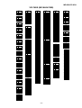
Traffic Programme code Traffic Announcement code
(TP)
(TA)
OFF
OFF
OFF
ON
ON
OFF
ON
ON
Applications
This programme does not carry traffic announcements nor does
it refer, via EON, to a programme that does.
This programme carries EON information about another
programme which gives traffic information.
This programme carries traffic announcements but none are
being broadcast at present and may also carry EON information
about other traffic announcements.
A traffic announcement is being broadcast on this programme at
present.
– 19 –
MD-X5H/CP-X5H
MD SECTION
• Note
Remove the MD unit for repeir, and after installing it in the set, be dure to reset it and ascertain that reset has been done.
Resetting procedure
(1) Unplug the AC cord from the socket, and hold down the RESET buttonm provided at the rear side
for more than 10 seconds.
(2) Once set the TEST MODE (holding down the TEST MODE (X-BASS botton) and
botton
together, press the POWER button), and then turn off power.
1. Preparation for adjustment
Test disc
Type
1
2
3
Test disc
Part No.
High reflection disc TGYS1 (SONY)
RRCDT0101AFZZ
Low reflection disc Recording minidisc
UDSKM0001AFZZ
Head Adjusting transparent RRCDT0103AFZZ
Extension Cable (See Fig. 30-4)
Type
1
2
3
4
3
Part No.
Extension PWB for servicing
Extension Connector (2 Pin)
Extension Connector (6 Pin)
Extension Cable (5 Pin)
Extension Cable (28 Pin)
RUNTK0457AFZZ
QCNWK0059AFZZ
QCNWK0107AFZZ
QCNWK0109AFZZ
QCNWK0108AFZZ
2. Test mode
Test mode setting method
1. Holding down the
+ button and MD
(PLAY/PAUSE) button, press the POWER button.
(State A is changed to state B .)
2. Insert the playback disc 1 (high reflection disc) or recording disc 2 (low reflection disc). (State C is set.)
Thus, the test mode state is set.
A tsm
TEST
e
: TEST MODE
STOP state
represents version of MD microcomputer.
(When the MD (STOP) button is ressed in the C state, the indication A
is restored. To restore C again, press the CD
(PLAY/ PAUSE)
button.)
B EJECT
TEST
C AUT YOBI
TEST
Entering the specific mode
Whenever the CD
(PLAY/PAUSE) button is pressed, the mode is changed.
AUTO pre-adjustment
AUTO adjustment
RESULT Pre-adjustment
EEPROM setting
MANUAL adjustment
MANUAL pre-adjustment
RESULT MANUAL pre-adjustment
• Canceling the test mode
When the POWER button is pressed, the test mode is canceled, and the POWER OFF state is set.
– 20 –
MD-X5H/CP-X5H
• Test Mode
1. AUTO pre-adjustment mode
• Automatic pre-adjustment is performed. (After adjustment the grating adjustment mode is set.)
• The adjustment value is output with the aid of system controller interface.
2. AUTO adjustment mode
• Automatic adjustment is performed.
• The adjustment value is output with the aid of system controller interface.
• Continuous playback is performed. (Error rate indication, jump test)
3. RESULT sub-mode
• The measurement value, set value and calculated value are indicated.
• The set value is changed manually (in servo OFF state).
4. RESULT mode (final adjustment)
• The set value (after calculation) is indicated.
• The set value is changed manually (in servo OFF state).
5. MANUAL pre-adjustment mode
• RF side manual adjustment is performed.
• Focus and tracking signal ATT manual adjustment is performed.
• Focus and tracking signal offset setting is performed.
6. MANUAL adjustment mode
• Focus and tracking signal ATT manual adjustment is performed.
7. EEPROM setting mode
• Various coefficients of digital servo are changed manually.
• Each servo is set to ON individually.
• Temperature detection terminal voltage is measured, and the reference value is determined.
8. TEST-PLAY mode
• Continuous playback from the specified address is performed.
• C1 error rate measurement, ADIP error rate measurement.
9. TEST-REC mode
• Continuous recording from the specified address is performed.
• Change of record laser output (servo gain is also changed according to laser output)
10. INNER mode
• The position where the INNER switch is turned on is measured.
11. EJECT mode
• TEMP setting (of EEPROM setting)
• CONTROL setting (of EEPROM setting)
• Setting of laser power (record/playback power)
1. AUTO pre-adjustment mode (Low reflection disc only)
Step No.
Step 1
•
Setting Method
Remarks
Testmode STOP state
Display
[tsm
e
]
Step 2
Press once the CD PLAY button. AUTO pre-adjustment menu
[_AUT_YOBI_]
Step 3
Press once the MD PLAY button. The slide moves to the innermost periphery, and automatic
pre-adjustment is started.
• During automatic adjustment
changes as follows.
HAo→RFg→SAg→SBg→PTG→PCH→GTG→GCH→RCG→
SEG→RFG→SAG→HAO→HEO→TCO→LAO
End of adjustment
If adjustment is OK, Step 4.
If adjustment is NG, Step 5.
[
Step 4
Grating adjustment,
adjustment value output
Press once the MD STOP button. STEP 2
[_COMPLETE_]
Step 5
Adjustment value output
Press once the MD STOP button. STEP 2 AUTO pre-adjustment menu
[ Can't _ ADJ. ]
: Adjustment name,
: Address
– 21 –
:______]
MD-X5H/CP-X5H
2. AUTO adjustment mode
Step No.
•
Setting Method
Remarks
Display
Step 1
Testmode STOP state
[tsm
Step 2
Press the CD PLAY button two times. AUTO adjustment menu
[AUTO_AJST_]
Step 3
Press once the MD PLAY button. The slide moves to the innermost periphery, and automatic
adjustment is started.
• In case of high reflection disc
changes as follows.
PEG→HAG
•In case of low reflection disc
changes as follows.
PEG→LAG→GCG→GEG→LAG
End of adjustment
If adjustment is OK, Step 4.
If adjustment is NG, Step 7.
[
Step 4
Adjustment value output
Press the MD PLAY button.
Press the MD STOP button.
[_COMPLETE_]
]
:______]
STEP 5
STEP 2
Step 5
Continuous playback (pit section)
Continuous playback (groove section)
Step 6
Press the CD STOP button.
Press the MD STOP button.
Continuous playback (groove section)
STEP 2 AUTO adjustment menu
Step 7
Adjustment value output
Press the MD STOP button.
STEP 2 AUTO adjustment menu
: Adjustment name,
e
[s
[a
c
c
]
]
[a
a
]
[ Can't _ ADJ. ]
: Measurement value,
: Address
3. RESULT sub-mode
Step No.
Step 1
Setting Method
Remarks
Display
Testmode STOP state
[tsm
Step 2
Press the CD PLAY button three times. RESULT sub-menu
[_RST_YOBI_]
Step 3
Press once the MD PLAY button. Indication of measurement value
[RFG:_
__
]
Step 4
Press once the CD PLAY button. Indication of measurement value
[RCG:_
__
]
Step 5
Press once the CD PLAY button. Indication of measurement value
[RTG:_____
Step 6
Press once the CD PLAY button. Indication of measurement value
[GTG:__ _ _ _
]
Step 7
Press once the CD PLAY button. Indication of measurement value
[PCH:____
]
Step 8
Press once the CD PLAY button. Indication of measurement value
[GCH:____
]
Step 9
Press once the CD PLAY button. Indication of measurement value
[SAG:___
]
Step 10
Press once the CD PLAY button. Indication of measurement value
[SBG:___
]
Step 11
Press once the CD PLAY button. Indication of measurement value
[SEG:___
]
Step 12
Press once the CD PLAY button. Indication of measurement value
[SFG:__ _
]
Step 13
Press once the CD PLAY button. Indication of measurement value
[HAO:
_ _ _]
Step 14
Press once the CD PLAY button. Indication of measurement value
[HBO:
_ _ _]
Step 15
Press once the CD PLAY button. Indication of measurement value
[HEO:
_ _ _]
Step 16
Press once the CD PLAY button. Indication of measurement value
[HFO:
_ _ _]
Step 17
Press once the CD PLAY button. Indication of measurement value
[LAO:
_ _ _]
Step 18
Press once the CD PLAY button. Indication of measurement value
[LBO:
_ _ _]
Step 19
Press once the CD PLAY button. Indication of measurement value
[LEO:
_ _ _]
Step 20
Press once the CD PLAY button. Indication of measurement value
[LFO:
_ _ _]
Step 21
Press once the CD PLAY button. Indication of measurement value
[TCO:_
_ _ _]
Step 22
Press once the CD PLAY button. Indication of adjustment error sequence No.
[YOB:_
_ _ _]
Step 23
Press once the CD PLAY button. Indication of adjustment status
[D I F:_
_ _ _]
Step 24
Press once the CD PLAY button. Indication of pre-adjustment not completed (00)/completed (4B)
[ADJ:_
_ _ _]
Step 25
Press once the MD PLAY button. RESULT sub-menu state
[_RST_YOBI_]
: Measurement value,
: Adjustment value,
: Other various informations
•
• ressing the REC button causes reversing.
• If the VOL UP button is pressed while the set value is indicated, the set value increases, and the new set value is stored in RAM.
• If the VOL DOWN button is pressed while the set value is indicated, the set value reduces, and the new set value is stored in RAM.
• If the VOL UP/VOL DOWN button is held down, the set value changes continuously with 100 ms cycle.
• The digit of increase/decrease by the VOL UP/VOL DOWN button can be shifted with the aid of CD STOP button.
– 22 –
e
]
]
MD-X5H/CP-X5H
3. RESULT mode (final adjustment)
Step No.
Step 1
Setting Method
Remarks
Testmode STOP state
Display
[tsm
RESULT menu
e
]
Step 2
Press the CD PLAY button four times.
Step 3
Press once the MD PLAY button. Indication of set value
[_RESULT___]
[HAG:__ _
]
Step 4
Press once the CD PLAY button. Indication of set value
[HBG:__ _
]
Step 5
Press once the CD PLAY button. Indication of set value
[LAG:__ _
]
Step 6
Press once the CD PLAY button. Indication of set value
[LBG:__ _
]
Step 7
Press once the CD PLAY button. Indication of set value
[PEG:__ _
]
Step 8
Press once the CD PLAY button. Indication of set value
[PFG:__ _
]
Step 9
Press once the CD PLAY button. Indication of set value
[GEG:__ _
]
Step 10
Press once the CD PLAY button. Indication of set value
[GFG:__ _
]
Step 11
Press once the CD PLAY button. Indication of set value
[GCG:__ _ _
]
Step 12
Press once the MD STOP button. RESULT menu state
[_RESULT___]
•
: Measurement value
• ressing the REC button causes reversing.
• If the VOL UP button is pressed while the set value is indicated, the set value increases, and the new set value is stored in RAM.
• If the VOL DOWN button is pressed while the set value is indicated, the set value reduces, and the new set value is stored in RAM.
• If the VOL UP/VOL DOWN button is held down, the set value changes continuously with 100 ms cycle.
• The digit of increase/decrease by the VOL UP/VOL DOWN button can be shifted with the aid of CD STOP button.
5. MANUAL auxiliary adjustment mode (only low reflection disc)
Step No.
•
Setting Method
Remarks
Display
Step 1
Testmode STOP state
[tsm
Step 2
Press the CD PLAY button five times. MANUAL auxiliary adjustment mode
[_MNU_YOBI_]
Step 3
Press once the MD PLAY button. Initial setting → Temperature measuring mode
[TMP:_
___]
Step 4
Press once the CD PLAY button. Offset "0" setting → A signal offset tentative measurement
[HAo:
___]
Step 5
Press once the CD PLAY button. B signal offset tentative measurement
[HBo:
___]
Step 6
Press once the CD PLAY button. E signal offset tentative measurement
[HEo:
___]
Step 7
Press once the CD PLAY button. F signal offset tentative measurement
[HFo:
___]
Step 8
Press once the CD PLAY button. Offset tentative measurement → Laser ON
[LON:______]
Step 9
Press once the CD PLAY button. Innermost periphery move → RF side FG rough adjustment
[RFg:
Step 10
Press once the CD PLAY button. Focus ATT (A signal) tentative setting
[SAg:
Step 11
Press once the CD PLAY button. Focus ATT (B signal) tentative setting
[SBg:
Step 12
Press once the CD PLAY button. RF side pit section TG adjustment
[PTG:
__
]
Step 13
Press once the CD PLAY button. Pit section COUT level setting
[PCH:
_
]
Step 14
Press once the CD PLAY button. Outer periphery move → RF side groove TG adjustment
[GTG:
__
]
Step 15
Press once the CD PLAY button. Groove section COUT level setting
[GCH:
_
]
Step 16
Press once the CD PLAY button. RF side TCRS adjustment
[RCG:
__
]
Step 17
Press once the CD PLAY button. Tracking ATT (E signal) setting
[SEG:
]
Step 18
Press once the CD PLAY button. Tracking ATT (F signal) setting
[SFG:
]
Step 19
Press once the CD PLAY button. Indication of tracking EFMIO measurement
[gMI:
___]
Step 20
Press once the CD PLAY button. RF side pit section FG adjustment
[R F G :
__
Step 21
Press once the CD PLAY button. Focus ATT (A signal) setting
[SAG:
]
Step 22
Press once the CD PLAY button. Focus ATT (B signal) setting
[SBG:
]
Step 23
Press once the CD PLAY button. Offset "0" setting → A signal offset measurement
[HAO:
___]
Step 24
Press once the CD PLAY button. B signal offset measurement
[HBO:
___]
Step 25
Press once the CD PLAY button. E signal offset measurement
[HEO:
___]
Step 26
Press once the CD PLAY button. F signal offset measurement
[HFO:
___]
Step 27
Press once the CD PLAY button. TCRS signal offset measurement
[TCO:
___]
Step 28
Press once the CD PLAY button. A signal offset measurement
[LAO:
___]
Step 29
Press once the CD PLAY button. B signal offset measurement
[LBO:
___]
Step 30
Press once the CD PLAY button. E signal offset measurement
[LEO:
___]
Step 31
Press once the CD PLAY button. F signal offset measurement
[LFO:
___]
: Measurement value,
: Set value,
: Account value
– 23 –
e
]
__
]
]
]
]
MD-X5H/CP-X5H
• If the VOL UP/VOL DOWN button is pressed during setting indication, the setting increases/decreases, and the new setting is stored in RAM.
• If the VOL UP/VOL DOWN button is held down, the setting changes continuously with 100 ms cycle.
• If the REC button is pressed, the setting returns step by step excepting the following case.
A signal offset (HAO) → Offset tentative setting → RF side FG adjustment (RFG)
RF side TCRS adjustment (RCG) → RF side groove TG adjustment (GTG)
RF side groove TG adjustment (GTG) → Innermost periphery move → RF side pit section adjustment (PTG)
RF side pit TG adjustment (PTG) → RF side FG rough adjustment (RFg) → Laser lighting (LON)
Laser lighting (LON) → Offset "0" setting → A signal offset tentative measurement (HAo)
If the measurement value is within the OK range, " " appears on the 8th character.
6. MANUAL adjustment mode
High reflection disc
Step No.
Setting Method
Remarks
Display
Step 1
Testmode STOP state
Step 2
Press the CD PLAY button six times.
[tsm
Step 3
Press once the MD PLAY button. Initial setting → Temperature measuring mode
[TMP:_
Step 4
Press once the CD PLAY button. Laser ON
[LON:______]
Step 5
Press once the CD PLAY button. Innermost periphery move → Tracking ATT (E signal) setting
[PEG:
]
Step 6
Press once the CD PLAY button. Tracking ATT (F signal) setting
[PFG:
]
Step 7
Press once the CD PLAY button. Indication of tracking EFMIO measurement
[PMI:
Step 8
Press once the CD PLAY button. Focus ATT (A signal) setting
[HAG:
]
Step 9
Press once the CD PLAY button. Focus ATT (B signal) setting
[HBG:
]
MANUAL adjustment menu
e
]
[_MNU_AJST_]
___]
___]
• If the MD STOP button is pressed while the MANUAL adjustment menu is displayed, the state is changed to the TEST mode STOP
state.
• If the REC button is pressed, the setting returns step.
Low reflection disc
Step No.
Step 1
Setting Method
Remarks
Testmode STOP state
Display
[tsm
MANUAL adjustment menu
e
]
Step 2
Press the CD PLAY button six times.
Step 3
Press once the MD PLAY button. Initial setting → Temperature measuring mode
[_MNU_AJST_]
[TMP:_
Step 4
Press once the CD PLAY button. Laser ON
[LON:______]
Step 5
Press once the CD PLAY button. Innermost periphery move → Tracking ATT (E signal) setting
[PEG:
]
Step 6
Press once the CD PLAY button. Tracking ATT (F signal) setting
[PFG:
]
Step 7
Press once the CD PLAY button. Indication of tracking EFMIO measurement (pit section)
[PMI:
___]
Step 8
Press once the CD PLAY button. Focus ATT (A signal) setting
[LAg:
]
Step 9
Press once the CD PLAY button. Focus ATT (B signal) setting
[LBg:
]
Step 10
Press once the CD PLAY button. Outside periphery move → Track closs setting
[GCG:
Step 11
Press once the CD PLAY button. Tracking ATT (E signal) setting
[GEG:
]
Step 12
Press once the CD PLAY button. Tracking ATT (F signal) setting
[PFG:
]
Step 13
Press once the CD PLAY button. Indication of tracking EFMIO measurement (groove section)
[GMI:
___]
Step 14
Press once the CD PLAY button. Focus ATT (A signal) setting
[LAG:
]
Step 15
Press once the CD PLAY button. Focus ATT (B signal) setting
[LBG:
]
___]
]
• If the MD STOP button is pressed while the MANUAL adjustment menu is displayed, the state is changed to the TEST mode STOP
state.
• If the REC button is pressed, the setting returns step by step excepting the following case.
Track closs ATT setting (GTG) → Innermost periphery move → Focus ATT (B signal) setting (LBg)
7. EEPROM setting mode
a) Focus setting
Step No.
Step 1
Setting Method
Remarks
Display
Testmode STOP state
[tsm
Step 2
Press the CD PLAY button seventimes. EEPROM setting menu
[E E P R O M _ S E T]
Step 3
Press once the MD PLAY button. Focus setting menu
[__Focus___]
Step 4
Press once the MD PLAY button. Focus system loop filter gain constant setting
[FG______
]
Step 5
Press once the CD PLAY button. Focus system loop filter f characteristic constant 1 setting
[FF1_____
]
Step 6
Press once the CD PLAY button. Focus system loop filter f characteristic constant 2 setting
[FF2_____
]
Step 7
Press once the CD PLAY button. FZC oscillation histerisis level setting a
[FZHLEV__
]
Step 8
Press once the CD PLAY button. Comparison level setting (normal) in case of FOK generation
[FOKLEVn_
]
– 24 –
e
]
MD-X5H/CP-X5H
Setting Method
Step No.
Remarks
Display
Step 9
Press once the CD PLAY button. Comparison level setting in case of FOK generation
(when focus is "ON")
[FOKLEV f_
]
Step 10
Press once the CD PLAY button. LPF coefficient setting (normal) in case of FOK generation
[FOKLPFn_
]
Step 11
Press once the CD PLAY button. LPF coefficient setting in case of FOK generation
(when focus is "ON")
[FOKLPFf_
]
Step 12
Press once the CD PLAY button. Waiting time setting in case of auto-focus retraction
[ W A I T f_ _ _
]
: Setting volue
•
• Pressing the REC button causes reversing.
• If the VOL UP button is pressed while the specific setting item is indicated, the setting increases, and the new setting is set in LSI.
• If the VOL DOWN button is pressed while the specific setting item is indicated, the setting decreases, and the new setting is set in LSI.
• If the VOL UP/VOL DOWN button is held down, the setting changes continuously with 100 ms cycle.
b) Spindle setting
Setting Method
Step No.
Remarks
Display
Step 1
Testmode STOP state
[tsm
Step 2
Press the CD PLAY button seven times. EEPROM setting menu
[E E P R O M _ S E T]
e
]
Step 3
Press once the MD PLAY button. Focus setting menu
[__Focus___]
Step 4
Press once the CD PLAY button. Spindle setting menu
[_Spindle__]
Step 5
Press once the MD PLAY button. Spindle system loop filter gain constant setting
(Until tracking servo ON)
[SPG_____
Step 6
Press once the CD PLAY button. Spindle system loop filter gain constant setting
(After tracking servo ON, inner periphery)
[SPG_in__
]
Step 7
Press once the CD PLAY button. Spindle system loop filter gain constant setting
(After tracking servo ON, center)
[SPG_mid_
]
Step 8
Press once the CD PLAY button. Spindle system loop filter gain constant setting
(After tracking servo ON, outside periphery)
[SPG_out_
]
Step 9
Press once the CD PLAY button. Spindle system loop filter f characteristic constant 1 setting
[SP1_____
]
Step 10
Press once the CD PLAY button. Spindle system loop filter f characteristic constant 2 setting
[SP2_____
]
Step 11
Press once the CD PLAY button. Spindle system loop filter f characteristic constant 3 setting
[SP3_____
]
Step 12
Press once the CD PLAY button. Spindle system loop filter f characteristic constant 4 setting
[SP4_____
]
Step 13
Press once the CD PLAY button. Spindle system loop filter f characteristic constant 5 setting
[SP5_____
]
Step 14
Press once the CD PLAY button. Spindle drive output limitter setting
[SPDLIM__
]
]
•
: Setting volue
• Pressing the REC button causes reversing.
• If the VOL UP button is pressed while the specific setting item is indicated, the setting increases, and the new setting is set in LSI.
• If the VOL DOWN button is pressed while the specific setting item is indicated, the setting decreases, and the new setting is set in LSI.
• If the VOL UP/VOL DOWN button is held down, the setting changes continuously with 100 ms cycle.
c) Tracking setting
Step No.
Setting Method
Remarks
Display
Step 1
Testmode STOP state
[tsm
Step 2
Press the CD PLAY button seven times. EEPROM setting menu
[E E P R O M _ S E T]
Step 3
Press once the MD PLAY button. Focus setting menu
[__Focus___]
Step 4
Press the CD PLAY button two times. Tracking setting menu
[_Tracking_]
Step 5
Press once the MD PLAY button. Tracking system loop filter gain constant setting
[TG______
]
Step 6
Press once the CD PLAY button. Spindle system loop filter f characteristic constant 1 setting
[TF1_____
]
Step 7
Press once the CD PLAY button. Spindle system loop filter f characteristic constant 2 setting
[TF2_____
]
Step 8
Press once the CD PLAY button. Setting of tracking system servo mode 4
[SVCNT4__
Step 9
Press once the CD PLAY button. Tracking deceleration pulse level setting (for one line jump)
[TRBLV0__
Step 10
Press once the CD PLAY button. Tracking deceleration pulse level setting (for 10 line jump)
[TRBLVt__
Step 11
Press once the CD PLAY button. Tracking kick pulse level setting (for one line jump)
[TRKLV0__
Step 12
Press once the CD PLAY button. Tracking kick pulse level setting (for 10 line jump)
[TRKLVt__
Step 13
Press once the CD PLAY button. Tracking drive pulse width setting (for one line jump)
[TDPWo___
Step 14
Press once the CD PLAY button. Tracking drive pulse width setting (for 10 line jump)
[TDPWt __
Step 15
Press once the CD PLAY button. Tracking slip stop time setting (for one line jump)
[SLCT0___
Step 16
Press once the CD PLAY button. Tracking slip stop time setting (for 10 line jump)
[SLCTt___
Step 17
Press once the CD PLAY button. Tracking slip stop time setting (move)
[SLCTm__
– 25 –
e
]
]
]
]
]
]
]
]
]
]
]
MD-X5H/CP-X5H
Setting Method
Step No.
Remarks
Display
Step 18
Press once the CD PLAY button. TCRS comparison level 1 for high reflection
[TCRSC1P_
]
Step 19
Press once the CD PLAY button. Comparison level in case of COUT generation (playback)
[COTLVp__
]
Step 20
Press once the CD PLAY button. Comparison level in case of COUT generation (pecord)
[COTLVr__
]
Step 21
Press once the CD PLAY button. Auto-move waiting time setting
[ W A I T m_ _ _
]
•
: Setting volue
• Pressing the REC button causes reversing.
• If the VOL UP button is pressed while the specific setting item is indicated, the setting increases, and the new setting is set in LSI.
• If the VOL DOWN button is pressed while the specific setting item is indicated, the setting decreases, and the new setting is set in LSI.
• If the VOL UP/VOL DOWN button is held down, the setting changes continuously with 100 ms cycle.
d) Slide setting
Step No.
Setting Method
Remarks
Display
Step 1
Testmode STOP state
[tsm
Step 2
Press the CD PLAY button seven times. EEPROM setting menu
[E E P R O M _ S E T]
e
]
Step 3
Press once the MD PLAY button. Focus setting menu
[__Focus___]
Step 4
Press the CD PLAY button three times. Slide setting menu
[___Sled___]
Step 5
Press once the MD PLAY button. Slide system loop filter gain constant setting
[SLG_____
]
Step 6
Press once the CD PLAY button. Slide system loop filter f characteristic constant 2 setting
[SL2_____
]
]
Step 7
Press once the CD PLAY button. Slide output limitter setting
[SLDLIM__
Step 8
Press once the CD PLAY button. Slide servo output dead zone level setting
[SLDLEV__
]
Step 9
Press once the CD PLAY button. Slide kick pulse level setting (forced move)
[SLKLVk__
]
Step 10
Press once the CD PLAY button. Slide kick pulse level setting (for 10 lines jump auxiliary use)
[SLKLVt__
]
Step 11
Press once the CD PLAY button. Slide kick pulse level setting (move)
[SLKLVm__
]
: Setting volue
•
• Pressing the REC button causes reversing.
• If the VOL UP button is pressed while the specific setting item is indicated, the setting increases, and the new setting is set in LSI.
• If the VOL DOWN button is pressed while the specific setting item is indicated, the setting decreases, and the new setting is set in LSI.
• If the VOL UP/VOL DOWN button is held down, the setting changes continuously with 100 ms cycle.
Temperature measurement value correction table
EEPROM record value = Microcomputer measurement value +
Correction
Ambient temperature
correction
12.2 °C ~ 15.8 °C
-0 3 H
15.9 °C ~ 19.6 °C
-0 2 H
* EEPROM record value
19.7 °C ~ 23.2 °C
-0 1 H
23.2 °C ~ 26.8 °C
±0H
26.9 °C ~ 30.7 °C
+0 1
H
30.8 °C ~ 34.3 °C
+0 2
H
34.4 °C ~ 37.9 °C
+0 3
H
Value to be measured by the microcomputer at +25°C
* Microcomputer measurement value
Value to be measured by the microcomputer at specific
temperature
* Correction value
Correction value for conversion to measurement value at
+25°C (see the table shown left)
• Temperature code check
The temperature code is read after automatic adjustment. If it is within the range shown below, the adjustment is OK.
Ambient temperature
temperature code
19.6 °C ~ 30.7 °C
06
8.7 °C ~ 19.6 °C
07
– 26 –
MD-X5H/CP-X5H
e) TEMP setting
Setting Method
Step No.
Remarks
Display
Step 1
Testmode STOP state
[tsm
Step 2
Press the CD PLAY button seven times. EEPROM setting menu
[E E P R O M _ S E T]
Step 3
Press once the MD PLAY button. Focus setting menu
[__Focus___]
Step 4
Press the CD PLAY button four times.
[___Temp___]
Step 5
Press once the MD PLAY button. TEMP reference value setting
TEMP setting menu
Setting Method
Step No.
e
[TEMP_
Remarks
]
_
]
Display
Step 1
EJECT state (or mechanism-less state)
[__EJECT___]
Step 2
Press the CD
[TEMP_
MD EDIT button. TEMP reference value setting
_
]
•
: Setting volue,
: Measurement value
• If the VOL UP button is pressed while the specific setting item is indicated, the setting increases, and the new setting is set in LSI.
• If the VOL DOWN button is pressed while the specific setting item is indicated, the setting decreases, and the new setting is set in LSI.
• If the VOL UP/VOL DOWN button is held down, the setting changes continuously with 100 ms cycle.
f) CONTROL setting
Step No.
Setting Method
Remarks
Display
Step 1
Testmode STOP state
[tsm
Step 2
Press the CD PLAY button seven times. EEPROM setting menu
[E E P R O M _ S E T]
Step 3
Press once the MD PLAY button. Focus setting menu
[__Focus___]
Step 4
Press the CD PLAY button five times.
[_Control__]
Step 5
Press once the MD PLAY button. CONTROL 1 setting
[ C O N T R L 1_
]
Step 6
Press once the CD PLAY button. CONTROL 2 setting
[ C O N T R L 2_
]
Step 7
Press once the CD PLAY button. Setting of spin kick level in MOVE state
[ S P K L E V m_
]
Step 8
Press once the CD PLAY button. Setting of readjustment interval time (minutes)
[ A D J T T M_ _
]
Step 9
Press once the CD PLAY button. Setting of equalizer coefficients A and D (high reflection)
[ H D E Q A D_ _
]
Step 10
Press once the CD PLAY button. Setting of equalizer coefficients A and D (low reflection pit)
[ L D E Q A D_ _
]
Step 11
Press once the CD PLAY button. Setting of equalizer coefficients A and D (low reflection groove) [ G D E Q A D_ _
]
Step 12
Press once the CD PLAY button. Setting of equalizer coefficients B and C (high reflection)
[ H D E Q B C_ _
]
Step 13
Press once the CD PLAY button. Setting of equalizer coefficients B and C (low reflection pit)
[ L D E Q B C_ _
]
Step 14
Press once the CD PLAY button. Setting of equalizer coefficients B and C (low reflection groove) [ G D E Q B C_ _
Step 15
Press once the CD PLAY button. Setting of autolevel slicer gain (high reflection)
[ H A L S G_ _ _
Step 16
Press once the CD PLAY button. Setting of autolevel slicer gain (low reflection pit)
[ L A L S G_ _ _
Step 17
Press once the CD PLAY button. Setting of autolevel slicer gain (low reflection groove)
[GALSG__
Step 18
Press once the CD PLAY button. Setting of autolevel slicer offset (high reflection)
[ H A L S O F_ _
Step 19
Press once the CD PLAY button. Setting of autolevel slicer offset (low reflection pit)
[LALSOFS__
]
Step 20
Press once the CD PLAY button. Setting of autolevel slicer offset (low reflection groove)
[GALSOFS__
]
Step No.
CONTROL setting menu
Setting Method
Remarks
e
]
]
]
]
]
]
Display
Step 1
EJECT state (or mechanism-less state)
[__EJECT___]
Step 2
Press the TRACK EDIT button.
CONTROL 1 setting
[ C O N T R L 1_
]
Step 3
Press once the CD PLAY button. CONTROL 2 setting
[ C O N T R L 2_
]
•
: Setting volue
• If the VOL UP button is pressed while the specific setting item is indicated, the setting increases, and the new setting is set in LSI.
• If the VOL DOWN button is pressed while the specific setting item is indicated, the setting decreases, and the new setting is set in LSI.
• If the VOL UP/VOL DOWN button is held down, the setting changes continuously with 100 ms cycle.
• CONTROL 1
Pit 7
: High frequency superposition ON/OFF in record mode (0:OFF, 1:ON)
Pit 6~4
: Play start SD number (30 to 100 sector, 10 sector step)
Pit 2~0
: High speed jump over-run (384 to 830 lines, 64 lines step)
• CONTROL 2
Pit 4~0
: EEPROM version (a~)
– 27 –
MD-X5H/CP-X5H
8. TEST-PLAY mode
Setting Method
Step No.
Remarks
Display
Step 1
Testmode STOP state
[tsm
Step 2
Press the CD
[TEST_PLAY_]
Step 3
Press once the CD STOP button. ADRES setting (Target address initial value is indicated)
Press once the MD PLAY button. While searching, set the search output to "H". To start continuous play,
return it to "L".
[ADRES_0050]
Step 4
Continuous playback (pit section) (Address + C1 error indication)
Continuous playback (groove section) (Address + C1 error indication)
[s
[a
c
c
]
]
Step 5
Press once the CD STOP button. (Address + ADIP error indication)
Continuous playback (groove section)
[a
a
]
Step 6
Press once the MD STOP button. TEST-PLAY menu
[TEST_PLAY_]
MD EDIT button. TEST-PLAY menu
e
]
………
• If the MD STOP button is pressed while the TEST-PLAY menu is displayed, TEST mode STOP state is set.
• If the MD PLAY button is pressed while the TEST-PLAY menu is displayed, continuous playback is started from the current pickup position.
• Whenever the CD MD EDIT button is pressed in the address setting mode, the address changes as follows.
0 0 5 0 → 0 3 C 0 → 0 7 0 0 → 0 8 A 0 → 0 0 5 0 → …………
/
+ changes as follows.
• Whenever the CD STOP button is pressed in the address setting mode, the digit which is changed with 0 0 5 0 → 0 0 5 0 → 0 0 5 0 → 0 0 5 0 → …………
• The digit of address which has been specified with /
+ and CD STOP button in the address setting mode is set to +01H/-01H.(0~F)
* If the /
+ button is held down, the setting changes continuously with 100 ms cycle.
• If the TRACK EDIT button is pressed in the continuous playback mode, the number of jump lines changes as follows.
1 line → 10 line → 400 line → 1 line → …………
* After the number of jump lines is indicated for one second, the address indication is restored.
[
TR_JUMP]
/
+ button is pressed in the continuous playback mode, the specified number of lines is jumped in the FWD/REV
• If the direction.
* If the /
+ button is held down, the setting changes with 100 ms cycle.
• Whenever the CD STOP button is pressed in the continuous playback mode, the indication changes as follows.
* Pit section Continuous playback (SUBQ address indication + C1 error indication) remains.
[s
c
]
c
]
* Groove section
Continuous playback (ADIP address indication + C1 error indication) remains.
[a
↓
Continuous playback (ADIP address indication + ADIP error indication) remains.
[a
a
]
↓
c
]
Continuous playback (ADIP address indication + C1 error indication) remains.
[a
↓
: Adress,
•
: Error late,
: Jump lines
9. TEST-REC mode
Step No.
Setting Method
Remarks
Display
Step 1
Testmode STOP state
[tsm
Step 2
Press the CD
[TEST_REC__]
Step 3
Press once CD STOP button.
Step 4
Step 5
MD EDIT button. TEST-REC menu
ADRES setting (indication of address initial value)
e
]
[a0050_pw
]
Press once the MD PLAY button. While searching, set the search output to "H". To start continuous play,
return it to "L".
Continuous recording
[a
]
Press once the MD STOP button. TEST-REC menu
[TEST_REC__]
pw
• If the MD STOP button is pressed while the TEST-PLAY menu is displayed, TEST mode STOP state is set.
• If the MD PLAY button is pressed while the TEST-REC menu is displayed, continuous record is started from the current pickup position.
• Whenever the CD MD EDIT button is pressed in the address setting mode, the address changes as follows.
0 0 5 0 → 0 3 C 0 → 0 7 0 0 → 0 8 A 0 → 0 0 5 0 → …………
/
+ changes as follows.
• Whenever the CD STOP button is pressed in the address setting mode, the digit which is changed with 0 0 5 0 → 0 0 5 0 → 0 0 5 0 → 0 0 5 0 → …………
• The digit of address which has been specified with /
+ and CD STOP button in the address setting mode is set to +01H/-01H.(0~F)
* If the /
+ button is held down, the setting changes continuously with 100 ms cycle.
• If the VOL UP/VOL DOWN button is pressed in TEST-REC mode and continuous record mode, the laser record power changes.
(Servo gain changes also according to the record power.)
•
: Adress,
: Laser power cord
– 28 –
MD-X5H/CP-X5H
10. INNER mode
Setting Method
Step No.
Remarks
Display
Step 1
Testmode STOP state
Step 2
Press the TRACK EDIT button.
[tsm
Step 3
Press once the MD PLAY button. INNER switch position measurement
(SUBQ address and C1 error are also indicated.)
[s
Step 4
Press once the MD STOP button. INNER menu
[__INNER__]
INNER menu
e
]
[__INNER__]
c
]
: Adress
•
• Press the MD STOP button while the INNER menu is displayed, to shift to the TEST mode STOP state.
11. EJECT mode
Step No.
Setting Method
Remarks
Display
Step 1
Testmode EJECT state
[__EJECT___]
Step 2
Press oncethe CD STOP button.
Step 3
Press once the CD STOP button. Record power output state
[rpw_______]
Step 4
Press once the CD STOP button. Playback power output state
[ppw_______]
Step 5
Press the CD
Step 6
Press the TRACK EDIT button.
Max. power output state
[xpw_______]
MD EDIT button. TEMP setting of EEPROM setting
(Refer to TEMP setting of EEPROM)
CONTROL setting of EEPROM setting
(Refer to CONTROL setting of EEPROM)
Lead-in switch position measurement mode
Note: Adjust the lead-in switch position to 5FF85 to FFD2.
1. Loosen the screw (A) x 3 pcs. which fix the mechanism switch PWB.
2. Retighten the screw, pressing the mechanism switch PWB in the arrow direction, and then measure the lead-in switch position again.
After position adjustment fix with the three screws (A). (See Fig. 29.)
Note: After tightening the two screws on the PWB apply Screw Lock.
Loosen the
three screws (A).
Lead-In Switch
Mechanism Switch PWB
Figure 29
Forced rotation of loading motor
While the display indication is test mode STOP state or EJECT state,
the loading motor can be forcibly rotated by press theVOL UP/DOWN
button.
– 29 –
MD-X5H/CP-X5H
Mechanism Adjustment
1. Optical pickup grating inspecting method
1
3
2
42 pin of IC 1101
GND (TP1131)
26 pin of IC 1101
EOUT (TP1133)
OSILLOSCOPE
470p
GND CH1
CH2
470p
25 pin of IC 1101
FOUT (TP1132)
a
100K
X
100K
b
Y
Spindle Motor
LISSAJOUS'S WAVEFORM
Less thana:b = 3:1
Figure 30-1 Optical Pickup Grating Deviation
Measuring Method
After the automatic adjustment is performed in the AUTO mode (test
mode) with the aid of high refection MD disc ("COMPLATE" is
displayed), the Lissajous's waveform (x-y) is adjusted.
1. Slightly loosen the 3 screws of spindle moto, and maken an
adjustment, observing the Lissajous's waveform.
2. After adjustment tighten the screw in arder of 1 , 2 , 3 .
Adjusting hole
3
Spindle motor
1
adjusting
hole
Check the Lissajou's waveform,
shifting the mounting position with
a screwdriver (to be fitted into the
disc motor adjusting hole).
2
2. Jitter adjustment and checking method
Figure 30-2
jitter Meter
1pin of IC 1201 (TP1274)
EFMMON
88 pin of IC 1201 (TP1275)
GND
Figure 30-3 Jitter connection diagram
After performing automatic adjustment in AUTO mode of TEST mode
using the low reflection MD disc, check this jitter in pit continuous
playback and groove continuous playback mode.
2P extension connector
QCNWK0059AFZZ
5P extension flat cable
QCNWK0109AFZZ
From Magnetic Head
CNP1252
From
motor
From mechanism switch
PWB
CNP1601(Bottom side)
From Optical
Pickup Unit
CNP1602
CNP1603
CNP1604(Bottom side)
CNP1101
MD Main PWB
6P-2P extension connector
QCNWK0107AFZZ
28Pextension flat cable
QCNWK0108AFZZ
Figure 30-4
– 30 –
Extension PWB for service
(RUNTK0457AFZZ)
Fit the extension PWB for service to the mechanism
MD-X5H/CP-X5H
EXPLANATION OF ERROR DISPLAY
Error display
Corrective action
Errors
Can't REC
• Defect occurred successively 10 times during REC-PLAY.
• Check that the disc is free from flaw, dust
• As a result of occurrence of defect during REC-PLAY the
and fingerprint.
recordable cluster became zero.
Check whether there is any black spot.
• Adress is unreadable. REC state connot be set for 20 seconds
Check for disc disalignment and run-out.
although retry is repeated.
Can't COPY
• The following judgement is made according to the channel
status of digital signal which was input from D-IN during RECPAUSE or REC-PLAY.
(1) Other than audio signal
(2) Other than signals of home-use appliances
(3) Copy NG due to inversion of copy bit in CD.
• Check whether CD is copy-inhibited one.
(An exabple: CD-R)
Din UNLOCK
• The digital signal which was input from D-IN during RECPAUSE, REC-PLAY or CD FUNC playback caused the
following.
(1) PLL of digital IN was unlocked.
(2) Locking occurred in condition other than FS = 44.1 kHz
• Check whether there is any abnormality
in the D-IN signal line.
TOC FULL
• There were no areas to record music or character
infomation.(music name, disc name, etc.) during REC-PLAY.
• When an attempt to start is made, recordable area does not
remain.
• Replace the disc with a recording/
playback disc in which an area to register
UTOC remains.
UTOC ERR R
• ETNO > LTNO
• FTNO ≠ 0 or 1
• UTOC recorded on disc could not be read.
• UTOC data is not normal. Replace the
disc with other disc.
UTOC ERR A
• Start address > End address
• UTOC data is not normal. Replace the
disc with other disc.
UTOC ERR L0~4
• Any data of UTOC 0 to 4 looped.
• UTOC data is not normal. Replace the
disc with other disc.
NOT AUDIO
• Nonaudio data was recorded in the track mode of currently
selected TNO.
• Select other TNO or replace the disc with
other disc.
? DISC
• Data "MINI" of system ID which has been written in TOC with
ASCII code is not correct.
• The disc type written i TOC does not correcpond to pre/
mastered MD, recording MD and hybrid MD.
• The loaded disc is not applicable.
Replace the disc, and check.
DISC FULL
• When an attempt to set REC-PAUSE was made, there were no • Replace the disc with other recording disc
recordable areas.
in which recording area remains.
PLAYBACK MD
• An attempt to set REC-PAUSE or to start editing was made on • The loaded disc is a Playback-only disc.
the playback-only disc.
Replace the disc with a recording disc.
PROTECTED
• An attempt to record or edit was made on the record/playback
disc with its careless rease preventing tab being in rease
preventing state.
• An attempt was made t oedit the track which was writeprotected by information written in UTOC.
• Return the careless erase preventing tab
to its initial position, and redo.
• The track on which an attempt to edit was
made is a write-protected track. Redo on
another track.
Can't EDIT
• Specific editing conditions were not satisfied.
• The applied operation procedure is not
proper. Redo, applying the ocrrect
procedure.
TEMP OVER
• Owing to occurrence of some trouble internal temperature of
set (MD unit) rose excessively.
• Check by troubleshooting.
• Check whether the ambient temperature
is too high.
DISC ERR RD
PA
WR
• Read data was not correct or data could not be read correctly.
• Trouble occurred during recording if music data, resulting in
record failure.
• Data of TOC or UTOC is not normal or
disc las flaw. Replace the disc with other
disc.
TOC ERR S
TOC ERR R
TOC ERR T
• TOC was read but data was not correct.
• TOC could not be rad.
• The TOC information recorded on disc
does not conform to the MD standard.
Replace the disc with other disc.
• The disc has flaw. Replace the disc with
other disc.
UTOC W ERR
• Trouble occurred during rewriting of UTOC, resulting in UTOC
rewriting failure.
• The disc has flaw. Replace the disc with
other disc.
FOCUS ERROR
• After the disc was loaded, focusing failure occurred.
• Check that the disc is free from flaw,dust,
fingerprint and black spot. Check for disc
disalignment and run-out.
– 31 –
MD-X5H/CP-X5H
Error display
Corrective action
Errors
BLANK MD
• UTOC was read but total TNO and the number of characters of • Perform recording to check that the disc
is recordable disc.
NAME was 0?
DEFECT
• Focusing error was caused by shock during REC-PLAY.
• Check that the disc is free from flaw,dust,
fingerprint and black spot. Check for disc
disalignment and run-out.
TOC W ERROR
• Although UTOC can be read but UTOC cannot be rewritten.
• Check that the record head contact is
normal. Check that there is no broken
wire between PWB and the recording
head.
MD ERROR
• Data of EEPROOM is not correct.
• Once reset, and redo. If error occurs
persistently, replace EEPROM.
EXPLANATION OF MECHANISM ERROR
Errors
Error display
MECHA_ERR1_*
MECHA_ERR2_*
MECHA_ERR3_*
Ejection failure
Head-up failure
Head-down failure
* = E Ejection completion position
* = MHorizontal midway position
* = L Load completed position
* = D Head-down position
HINF (IC1401 97 PIN)
< 1.3 V
> 3.06 V
1.853~2.48 V
1.3~1.853 V
E2-PROM (IC402) writing procedure
1. Procedure to replace E2-PROM and to write the initial
value of microcomputer in E2-PROM
2. Temperature reference value setting procedure
(to be executed at room temperature within 21 to 29°C)
(1) Replace E2-PROM.
(2) Refer to the latest E2-PROM data list.
(3) Hold down the
button and MD PLAY button, and press the
POWER button to enter the test mode.
(4) Indication of version.
[tsm
e
]
E2-PROM version (c to z)
Microcomputer ROM version
Model code
(5) Press the CD PLAY key 7 times.
[EEPROM SET]
(6) Perform the operation shown in the "E2-PROM setting mode
chart", compare the indication with the E2-PROM data list, and
make a setting according to the E2-PROM data list, using VOL
UP botton or VOL DOWN button.
(7) Set the temperature reference value.
(Refer to "Temperature reference setting procedure".)
(8) The setting must conform to the E2-PROM data list.
(9) Turn off power supply to write in E2-PROM.
– 32 –
(1) Test mode stop state.
e
]
[tsm
(2) Crrect temperature depending on ambient temperature according
to the following table.
Ambient temperature
correction
12.2 °C ~ 15.8 °C
-0 3 H
15.9 °C ~ 19.6 °C
-0 2 H
19.7 °C ~ 23.2 °C
-0 1 H
23.2 °C ~ 26.8 °C
±0H
26.9 °C ~ 30.7 °C
+0 1
H
30.8 °C ~ 34.3 °C
+0 2
H
34.4 °C ~ 37.9 °C
+0 3
H
An example: When ambient temperature is 22°C and meadured
temperature is 73H
Temperature setting = 73 H - 01 H
= 72 H
* When the measured temperature fluctuates between
two values, take lower one (if temperature fluctuates
between 73H and 72H, take 72H).
(3) Press the CD PLAY button 7 times.
[EEPROM SET]
(4) Press the MD PLAY button 1 times.
[
FOCUS
]
(5) Press the CD PLAY button 4 times.
[
Temp
]
(6) Press once the MD PLAY button.
[TEMP
]
: Measured temperature,
: Temperature setting
(7) Set temperature to the value determined above, using the
VOL UP or VOL DOWN button.
(8) Press the MD STOP button.
[
Temp
]
MD-X5H/CP-X5H
E2-PROM Data List
Slide setting
Focus setting
Item indication
Item indication
Setting
Setting
FG
97
H
SLG
35
H
FF1
9E
H
SL2
27
H
FF2
E0
H
SLDLIM
65
H
FZHLEV
ED
H
SLDLEV
16
H
FOKLEVn
08
H
SLKLVk
55
H
FOKLEVf
88
H
SLKLVt
3A
H
FOKLPFn
00
H
SLKLVm
55
H
FOKLPFf
88
H
WAITf
90
H
Control setting
Item indication
Spin setting
Item indication
SPG
Setting
20
SPG—in
B8
H
H
SPG—mid
76
H
SPG—out
50
H
SP1
10
H
SP2
87
H
SP3
E3
H
SP4
E3
H
SP5
10
H
SPDLIM
78
H
Tracking setting
Item indication
TG
Setting
45
H
TF1
70
H
TF2
E0
H
SVCNT4
01
H
TRBLVo
53
H
TRBLVt
60
H
TRKLVo
4C
H
TRKLVt
38
H
TDPWo
89
H
TDPWt
1A
H
SLCTo
00
H
SLCTt
40
H
SLCTm
53
H
TCRSCIP
16
H
COTLVP
14
H
COTLVr
28
H
WAITm
FF
H
– 33 –
Setting
CONTRL1
80
H
CONTRL2
01
H
SPKLEVm
26
H
ADJTTM
14
H
HDEQAD
90
H
LDEQAD
8F
H
GDEQAD
91
H
MDEQBC
90
H
LDEQBC
8F
H
GDEQBC
8A
H
HALSG
21
H
LALSG
21
H
GALSG
21
H
HALSOFS
FE
H
LALSOFS
00
H
GALSOFS
00
H
REC
REC
REC
– 34 –
Figure 34
REC
REC
WAITf___
CD PLAY
FOKLPFf_
CD PLAY
REC
REC
FOKLPFn_
CD PLAY
FOKLEVf_
CD PLAY
FOKLEVn_
CD PLAY
FZCLEV__
CD PLAY
FF2_____
CD PLAY
CD PLAY
CD PLAY
CD PLAY
CD PLAY
CD PLAY
SPDLIM__
WAITm___
CD PLAY
COTLVr__
CD PLAY
COTLVp__
CD PLAY
SLCTm___
CD PLAY
SLCTt___
CD PLAY
SLCTo___
CD PLAY
TDPWt___
CD PLAY
CD PLAY
REC
TDPWo___
SP5_____
REC
TRKLVt__
CD PLAY
CD PLAY
SP4_____
TRKLVo__
SP3_____
REC
REC
CD PLAY
CD PLAY
TRBLVt__
REC
TRBLVo__
SP2_____
CD PLAY
SP1_____
CD PLAY
CD PLAY
REC
SVCNY4__
SPG_out_
REC
TF2_____
SPG_mid _
CD PLAY
CD PLAY
REC
TF1_____
CD PLAY
REC
SPG_in__
CD PLAY
CD PLAY
MD PLAY
TG _ _ _ _ _ _
FF1_____
Test mode STOP state
REC
REC
REC
REC
REC
REC
REC
REC
REC
REC
REC
REC
REC
REC
REC
_T r a c k i n g _
CD PLAY X2
SPG_____
MD PLAY
_Spindle__
CD PLAY
MD PLAY
FG______
REC
_ _ Focus_ _ _
MD PLAY
e
CD PLAY X7
REC
REC
REC
REC
REC
REC
SLKLVm__
CD PLAY
SLKLVt__
CD PLAY
SLKLVk__
CD PLAY
SLDLEV__
CD PLAY
SLDLIM__
CD PLAY
SL2_____
CD PLAY
SLG_____
MD PLAY
___S l e d___
CD PLAY X3
E E P R O M _ S E T EEPROM setting menu
tms
T E M P_
MD PLAY
_
_ _ _ Temp _ _ _
CD PLAY X4
CD MD
EDIT
GALSOFS_
CD PLAY
LALSOFS_
CD PLAY
HALSOFS_
CD PLAY
GALSG___
CD PLAY
LALSEG__
CD PLAY
HALSEG__
CD PLAY
GDEQBC__
CD PLAY
LDEQBC__
CD PLAY
HDEQBC__
CD PLAY
GDEQAD__
CD PLAY
LDEQAD__
CD PLAY
HDEQAD__
CD PLAY
ADJTTM__
CD PLAY
SPKLEVm_
CD PLAY
CONTRL2_
CD PLAY
CONTRL1_
MD PLAY
REC
REC
REC
REC
REC
REC
REC
REC
REC
REC
REC
REC
REC
REC
REC
_C o n t r o l _ _
TRACK
EJECT state
CD PLAY X5
_ _ EJECT _ _ _
MD-X5H/CP-X5H
E2-PROM Setting Mode Chart
MD-X5H/CP-X5H
NOTES ON SCHEMATIC DIAGRAM
• Resistor:
To differentiate the units of resistors, such symbol as K and M are
used: the symbol K means 1000 ohm and the symbol M means 1000
kohm and the resistor without any symbol is ohm-type resistor.
Besides, the one with “Fusible” is a fuse type.
• Capacitor:
To indicate the unit of capacitor, a symbol P is used: this symbol P
means micro-micro-farad and the unit of the capacitor without such
a symbol is microfarad. As to electrolytic capacitor, the expression
“capacitance/withstand voltage” is used.
(CH), (TH), (RH), (UJ): Temperature compensation
(ML): Mylar type
(P.P.): Polypropylene type
• Schematic diagram and Wiring Side of P.W.Board for this model are
subject to change for improvement without prior notice.
REF. NO
DESCRIPTION
• The indicated voltage in each section is the one measured by Digital
Multimeter between such a section and the chassis with no signal
given.
1. In the tuner section,
( ) indicates AM
< > indicates FM stereo
2. In the main section, a tape is being played back.
3. In the deck section, a tape is being played back.
( ) indicates the record state.
4. In the power section, a tape is being played back.
5. In the CD section, the CD is stopped.
• Parts marked with “ ” (
) are important for maintaining
the safety of the set. Be sure to replace these parts with specified
ones for maintaining the safety and performance of the set.
POSITION
REF. NO
SW701
OPEN/CLOSE
ON—OFF
SW732
MD-MD EDIT
ON—OFF
SW702
PICKUP IN
ON—OFF
SW733
TRACK
ON—OFF
SW705
PRE-EQ
ON—OFF
SW734
CD-MD EDIT
ON—OFF
SW706
X-BASS
ON—OFF
SW735
MD-REC
ON—OFF
SW708
MD-STOP
ON—OFF
SW736
MD-EJECT
ON—OFF
SW709
MD-PLAY/PAUSE
ON—OFF
SW738
VOLUME UP
ON—OFF
SW712
CD-PLAY/PAUSE
ON—OFF
SW739
VOLUME DOWN
ON—OFF
SW713
CD-STOP
ON—OFF
SW901
RESET
ON—OFF
SW717
CD-OPEN/CLOSE
ON—OFF
SW1952
DIRECT
ON—OFF
SW727
AUX
ON—OFF
SW1953
LEAD IN
ON—OFF
SW728
TUNER (BAND)
ON—OFF
SW1954
PLAY
ON—OFF
SW729
TRACK UP/TUNING UP
ON—OFF
SW1955
RECORD
ON—OFF
SW730
TRACK DOWN/TUNING DOWN
ON—OFF
SW1956
LOAD
ON—OFF
SW731
POWER
ON—OFF
B
(G)
3
TOP
VIEW
1
RN2404
RNC1407
RNC1404
RN1406
TOP
VIEW
2
FRONT
VIEW
C
(D)
FRONT
VIEW
POSITION
FRONT
VIEW
E
(S)
2SA1162 G
2SC2412 KR
2SK2909
KRC107 S
TOP VIEW
FRONT
VIEW
SB0209CP
DESCRIPTION
E C B
(S) (G) (D)
(1) (2) (3)
2SB562 C
2SC380 O
2SD467 D
2SD468 C
DTC363 TS
KRA107 M
KRC107 M
KTA1266 GR
KTC3199 GR
B C E
2SA1314 C
B C E
(D) (G) (S)
(3) (2) (1)
2SD2012
FRONT
VIEW
G D S
2SK1473
Figure 35 TYPES OF TRANSISTOR AND LED
– 35 –
E C B
2SB1238 R
Figure 36 BLOCK DIAGRAM (1/4)
– 36 –
M
M903
LOADING MOTOR
HEAD UP/DOWN
M
M902
SLED MOTOR
M
DIRECT SWITCH
SW1952
LEAD INSWITCH
SW1953
PLAYSWITCH
SW1954
RECSWITCH
SW1955
LOADING SWITCH
SW1956
WRITE PRO
LIGHT
RECEIVING
SECTION
RF
LIGHT
RECEIVING
SECTION
ERROR
SIGNAL
MD
Q1251~Q1254
D4.3V
MOTOR
DRIVER
IC1601
MONITOR DIODE
LASER DIODE
D3.2V
D6.5/4.75 ~ 5.25V
D3.2V
RF
SERVO/SIGNAL
CONTROL
IC1101
D4.3V
TRACKING
F
E–FSIGNAL A–BSIGNAL
A
B
E
RF1
RF1 ~ RF4SIGNAL
RF2
RF3
RF4
FOCUS
PICK UP UNIT
M901
SPINDLE MOTOR
RECORDING HEAD
HEAD DRIVE
SIGNAL
IC1251
D3.2V
D3.2V
PLL
D/A
CONVERTOR
A/D
CONVERTOR
A3.2V
DIGITAL
3.2V
4M
DRAM
ENDEC
ATRAC
IC1201
OSCILLATOR
XL1201
(33.8688MHz)
VOLTAGE
REGULATOR
POWER
D4.3V
VOLTAGE
REGULATOR
POWER
E2PROM
D3.2V
GND
DIGIN(EIAJ)
DIGOUT(EIAJ)
GND
AUDIO OUTPUT
AUDIO INPUT
MECHAN1SM
6.5/4.75~5.25V
BACKUP
MD
CONTROL
MICRO
COMPUTER
MD MICRO COMPUTER
3
4
1
2
1
2
3
4
5
6
7
8
9
10
11
12
13
14
15
16
17
18
19
20
21
22
23
24
L.OUT
AA.GND
R.OUT
KDATA
MDDATA
DSTB
D.GND
D.GND
D.GND
D.GND
DVDD
DVDD
AVCC
L.IN
AA.GND
R.IN
AD.GND
PDOWN
BACKUP
LOAD IN
RESET
MD-ST
DSCK
SERCH
MD-X5H/CP-X5H
– 37 –
Figure 37 BLOCK DIAGRAM (2/4)
M
M
PICK UP IN
SW702
M701
SPINDLE MOTOR
M702
SLED MOTOR
TRACKING COIL
FOCUS COIL
24
25
30
31
12
13
6
7
1
2
3
4
14 22 32
8 9
10 11
IC5
M56748FP
FOCUS/
TRACKING/
SPIN/
SLIDE/
DRIVER
1 5
+B1
PU-IN SW
SL+. SL–. DRF
PICK UP
IC1
IC2
CL, DAT, SELIAL CONTROL/CE
+5V
53 ~ 58 61
20 JP–
50 51 52 53
44
43
40
41
RES. CQCK. COIN
SQOUT. RWC. WRQ.4M
CV+
RFSM
SLC
SL
JP– 32
OPEN
SW701
CLOSE
26
27
28
29
34
35
36
20
30 31 54
15 16 27 23 29
FIN2
FIN1
E
F
IC2
LC78623D
9 EFMO SERVO/SIGNAL
10 EFMIN
CONTROL
12 CLV+
27 28
37
38
39
40
Q81
VOLTAGE
REGULATOR
LCHO
LVSS
RVSS
RCHO
23 36 41 43
6
44
45
+5V
CLK
CL
DAT
CE
IC1
LA9241M
SERVO AMP.
64
VCC1
62
LD0
XL1
16.934MHz
XIN
Q1
TO
FD
SPO
SP
SLD
XOUT
LASER DRIVER +5V
SL–
SL+
DRF
~
~
VVDD
VDD
LVDD
RVDD
XVDD
CONT4
CONT5
OPTICAL PICK UP UNIT
7
3
+7.3V (B2)
1 9
IC91
TA7291S
LOADING
MOTOR
DRIVER
6 5
M
M703
LOADING
MOTOR
TO MAIN SECTION
(TO µ-CON)
MD-X5H/CP-X5H
CNP301
AM LOOP
ANTENNA
2
1
3
9
12 13
AM
ANT.
COIL
T302
2
6
7
5V
8
7
2
4
2
4
X OUT
12
RDS
3
13
14
7
15
FM
20
20
ICT21
LC72720
Q360
+B4
1
24
22
23
AM IF
T351
4
8
9
5
IN GND
VCC
+B4
22
21
11
13
10
6
10
1
21
MPX
PHASE
11
FW303
17
7
VOLTAGE
REGULATOR
+B4
OUT
TO CD SERVO SECTION
8
3 4 5 6
IC302
TC72131
PLL
16
7
12
17
X351
IC303 FM IF DET./FM MPX./AM IF
IF
LA1832
2
OUT
AM OSC
1
OSC.
X352
4.5MHz
21
AM RF
FMOSC
VR351
FM MUTE
LEVEL
22
23
AM OSC.
AM RF
OSC. OUT
+B4
AM
OSC.
COIL
1
3
FM IF IN
MPX
IN CE
VSSA
DI
FM
OSC.
FM IF
AMP.
IN
CF302
VDDA
AFC
AM IN
5
CL
AM RF IN
FM IN
Q301
SD
1
DO
CF352
MONO/ST
FM MONO/ST
FM FRONT END
FE301
VSSD
8
VT
VDDD
IF IN
SO301
ANTENNA
TERMINAL
FM +B
X IN
STEREO
CE
DI
CL
Figure 38 BLOCK DIAGRAM (3/4)
DO
OUT
CF351
+5V
– 38 –
XT52
4.332MHz
+B4
MPX
VCO
CUT
FM IF
Q353
Q354
MUTING
16
MPX
IN
18
FM/AM
OUT
TUNER MUTE
L R
14 15
20
L354
SM
SD
AMP.
QT21
MD-X5H/CP-X5H
SO801
SPEAKER
– –
+
JK603
HEADPHONES
L–CH
JK652
DIGITAL2
COAXIAL
+
UNA651
DIGITAL 1
OPTICAL
R–CH
MD-X5H/CP-X5H
AC POWER SUPPLY CORD
AC230V
50Hz
C
1
3
1
IC554
NJM4558MF
OPE AMP.
5
M
IC652
74HCU04
INVERTER
31 32 33 34
T801
POWER TRANSFORMER
FAN MOTOR
M800
OM–OFF
FAN MOTOR
SW
Q895
Q801
F802
T2.5A
L250V
8
F803
T2A L
250V
–35V
12
IC904
INVERTER
74HC153P
13
16
–10V
IC712
FL Driver
IX0069AW
13 14
Q860
Q861
5/6.5V
Q851
Q850
+B 3
IC903
PST9140
RESET
–B
8 14
1
5 6 9 10 53
~
57
88 89
Q862
65 66
52
Q501
Q502
S-MUTE
84
43
27 29 32
+B1B
~
47
7V
9
X901
8MHz
IC901
SYSTEM MICROCOMPUTER
IX2718AF
IC501
LC75396E
AUDIO
PROCESSOR
25
27
29
36
72
81
~
49
63
52 60
54 58
L
L
R
5
14
2 14
R L
R L
Q421
Q423
Q424
R
AUX
OUT
MD
REC
Q541
Q542
D
1 15
JK650
AUX IN
Figure 39 BLOCK DIAGRAM (4/4)
– 39 –
B
L-MUTE
TO MD SECTION
1 7
IC651
MIC AMP.
NJM4558MF
3 5
J651
PHONO
MUTE
55 57
CD-MUTE
IC511
BU4052BC
FUNCTION
SELECTOR
53 59
FROM CD SECTION
23
FROM TUNER SECTION
4
FROM MD SECTION
1
3 13
SO601
Key Board
AUX
OUT
JK501B
23
TO TUNER SECTION
100
10V
64
48
GE
99
FROM MD SECTION
19
20
FROM CD
SECTION
46
FROM CD
SERVO SECTION
86
NAME IN
DISPLAY
RLY-OUT
E
~
C
6.0V
56
95
94
92
85
5.6V 9.6V
16 19 21
26
83
~
A MIC MUTE
L-MUTE
B
62
61
40
42
22
82
~
CD MUTE
+B4
~
D
+B1A
AUX IN
38
1
17 31
1 7
CD
MUTE
51
37
39
Q853
Q871
Q870
~
2
IC801
POWER AMP.
LA4451
1 6
3 4
18 16
RESET 3
+B1B
Q880
Q881
IC802
L-OUT
R-OUT
24
23
25
SW705,SW706,SW708
KEY SW709,SW712,SW713
SW717,SW727~736
SW738,SW739
FLDriver
Q891
8
2 14
7
Q891
Q802
DISPLY
SECTION
9
FROM MD SECTION
9
11
F806
T630mA L 250V
27
12
10
+B1B
2
F805
T630mA
L 250V
DISPLAY
FL711
D805~D808
~
D801~D804
5
+B4
8
IC552
NJM4565D
4
2 6
–B1
MD-X5H/CP-X5H
A
C342
0.022
0.022
C366 0.001
C367
1/16 R350 2.7K
0.022
C365
STEREO
VSM
AM IF IN
AM LOW CUT
GND
FM/AM OUT
SD
0.022
7
C354
CF352
1 3
AM IF
6
5
C353
33P
0.022
C344
C350
2
C364
4
L341
BALUN
D303
1SS133
D304
1SS133
IC
LA
FM I
/FM MP
3
3
C351 0.022
C352 10/16
D
1
2
1
2
18
20 19
21
AM RF IN
5.6K
R351
1
CF302
CNP301
AM LOOP
ANTENNA
22
FM IF IN
AM OSC OUT
AM MIX OUT
AM OSC IN
REG FM AFC
D302
1SS133
23
LO
F
R352
1K
0.022
24
R324
10K
D301
1SS133
C
C334
10/16
C333
0.022
C331
0.047
C332
0.022
C330
6.8P
(UJ)
C359
150P
L353
1mH
C363
R319 10K
R358
8.2K
10/16
VR351
10K(B)
FM MUTE
LEVEL
T302
0.022
AM ANT.
C362
3.3/50
C361
B
C343
33P
2
T351
R393
1K
C301
0.001
1K
1K
1K
R372
3
C387
0.022
6
FM VDD
FM IN
MW
AM IN
FM NC
MO/ST
IF IN
ST IND
5
IC302
LC72131
PLL
C380
10/16
R379
2.2K
CL
4
2
C385
0.01
AIN
DO PD
DI
1
R374
IF OUT
C382
15P
(CH)
R377
47K
L351
100µH
19 18 17 16 15 14 13 12
22 21 20
R373
F OUT
GND
VT
1
C393
1/50
X OUT
X IN
VSS
AOUT
CE
R349
33
C381
12P
(CH)
R347
6.8K
4 3 2
C397
C394 C392
0.022
47/16 0.001
R382
150
R380
R381
1.5K
10K
X352
4.5MHz
C347
0.022
+B
C341
0.022
VCC
ANT
3
R399
33
C348
0.01
FM IF AMP
Q301
2SC380 O
+B
FE 301
FM FRONT END
F
1
L342
2.2mmH
8 7 6 5
GND
GND
R301
120
R346
330
2
R348
680
R345
4.7K
C340
100/16
C345
0.022
C346
0.022
R369
82
E
R344
470
CF301
FM 75 ohms
SO301
ANTENNA
TERMINAL
7
8
9 10 11
C386
330P
R376
1K
R378
82K
+B
FM SIGNAL
AM SIGNAL
+B
R371
1K
Q371
KTA1266GR
MAIN PWB–A1(1/3)
G
H
• NOTES ON SCHEMATIC DIAGRAM can be found on page 35.
1
2
3
4
Figure 40 SCHEMATIC DIAGRAM (1/16)
– 40 –
5
6
Q
KRC
RT36
220K
RT35
220K
MD-X5H/CP-X5H
CT36
0.022
C370
1/50
R354
3.9K
CT28
47/10
CT29
0.022
19
18 17 16
CT25
560P
NC
9
VSSD
T3
T4
T5
8
NC
T2
7
SYNC
T1 RDS-ID
DO
FLOUT
6
RT21
100K
CT21
47/10
LT21
2.2µH
5
4
CT24
0.022
CT23
10/16
15 14 13
CIN
1 2 3
20
VDDD
XIN
TP
XOUT
TP
CT27
22P
(CH)
XT21
4.332MHz
R30 1K
R29 1K
R28 1K
VREF SYR
MPXIN CE
VDDA DI
CL
VSSA
24 23 22 21
D353
1SS133
R355
3.3K
C356
0.001
C355
22P
R393
1K
Q354
KTC3199GR
MUTING
C358
1/50
C357
2.2/50
0.022
C354
12
10 11 12
ICT21
LC72720
RDS
DECORDER
CT26
22P
(CH)
CT22
0.022
RT48
390
RT49
390
C399
0.022
C398
100/10
R352
1K
0.022
R353
270
C353
C374
0.039
10 11
LT22
2.2µH
CT43
10/16
VCC
MPX VCO
IF OUT MPX IN
PHASE
9
RT55
22K
RT26
1K
R367 C375
1K 3.3/50
R368
33K
R366
10K
R-CH OUT
L-CH OUT
PHASE
MO/ST
(FM/AM)
STEREO
FM DET
7 8
CF351
456kHz
AM LOW CUT
GND
FM/AM OUT
SD
6
5
C372 R362
1/50 470
R363
3.9K
MUTING
Q353
KTC3199GR
R365
10K
15 14 13
17 16
FM IF DET
/FM MPX/AM IF
C371R361
1/50 470
C369
27P
R356
1K
X351
IC303
LA1832
C368
1/50
C365
0.022
C366 0.001
C367
1/16 R350 2.7K
18
19
L354
LOW PASS
FILTER
R364
3.9K
C373
0.039
R357
470K
RT33
56K RT32
10K
TP
RT37
220K
QT21
RT34
56K KTC3199GR
CT37
0.022
ZDT21
L352 MTZJ5.1B
100µH ZD351
MTZJ5.1B
C396
100/16
C395
0.022
R377
47K
L351
00µH
+B R392
390
R391
Q360
390
KTA1266GR
C385
0.01
9 10 11
C386
330P
R395
47K
R385 R383
5.6K 5.6K
C391
47/16
R384
5.6K
D352
1SS133
R359
1.8K
FM NC
MO/ST
IF IN
ST IND
14 13 12
R376
1K
R360
4.7K
78
K
R370
1K
+B
+B
Q361
KRC107M
+B
+B
R387
22K
SD
D351
1SS133
TUN_RCH
TUN_GND
TUN_LCH
A_10V
Q371
1266GR
3
TUN MUTE
DI
CE
DO
CL
D GND
2
ZD352
MTZJ3.9B
SM
1
G G G
FW303
8
1
22 23 24 25
26 27 28
TO AUDIO SECTION
P42 4 - A, P43 7 - A
CNP303
TO CD SERVO PWB
P50 6 - H
7
8
9
10
Figure 41 SCHEMATIC DIAGRAM (2/16)
– 41 –
11
12
MD-X5H/CP-X5H
TO CD SERVO PWB
CNP904
P51 10 - H
TO TUNER SECTION
P40 10 - H
A
CNS904
1 2 3 4 5 6 7 8 9
CL
DI
CE
25
10 11 12
S_MUTE
AUX_A
AUX_B
L_MUTE
REC_RCH
REC_LCH
MD_LCH
MD_GND
MD_RCH
CD_RCH
CD_A_GND
CD_LCH
28 26 27
TO TUN
P41
J737
0.23µH
R692
22K
+B
R691 R693
22K 6.8K
R694
6.8K
R698
1.8K
A_10V
R697
1.8K
B
C573
82P
R569
18K
0V
0V
0V
R565
8.2K
0V
2
3
5
6
0V
–
+
1
0V
+
–
C576
C574 22/50
82P
10/50
C593
0.022
C591
R566
8.2K
C575
22/50
7
4 8
C
OPE AMP.
IC552
NJM4565M
R570
18K
C594
10/50
R505
47K
R461
3.9K
-9.5V
C592
0.022
+B
+B +B C549
0.022
9.5V
R462
3.9K
R463
1.2K
R464
1.2K
–B
C550
330/16
D557
1SS133
–B
D
R506 2
47K
C518
1/50
R696
1K
C52
0.22
C528
0.22/50
C530
0.027(ML)
C532
0.015(ML)
C534
0.0022(ML)
C536
0.0047
(ML)
E
C524
0.15/
C52
0.1/5
C538
1/50(N
C540
10/16
K820B
CNS820B
TO POWER AMP. PWB
CNS820A
P44 1 - C
C522
0.15/50
F
+B
1
2
3
4
5
6
7
+B
L_CH_OUT
A_GND
R_CH_OUT
A_10V
A_GND_OUT
A_-10V
HP_SW
+B
–B
–B
+B
+B
–B
D558
1SS133
A_GND
R523
15K
BI810
R525
22K
1
2
TO POWER AMP. PWB 3
CNP810
4
P44 1 - B
5
6
7
CNS810
G
FM SIGNAL
CD SIGNAL
MD PLAYBACK SIGNAL
MD RECORD SIGNAL
C555
0.001
C554
22/25
R597
2.2K
C821
0.0015
C822
0.0015
MAIN PWB - A1 (2/3)
H
• NOTES ON SCHEMATIC DIAGRAM can be found on page 35.
1
2
3
4
Figure 42 SCHEMATIC DIAGRAM (3/16)
– 42 –
5
6
R598
2.2K
MD-X5H/CP-X5H
TO TUNER SECTION
P41 10 - D
25 24 23 22
Q423
KTC3199GR
R431
5.6K
R427
100K
TUN_LCH
TUN_GND
TUN_RCH
LINE_R_IN
R432
5.6K
R428
100K
LINE_L_IN
LINE_GND
0V
0.7V
0V
R430
2.2K
3.4V
0V
AUX_IN-R
1/50
1/50
1/50
1/50
C501
C503
C505
C507
1K
1K
1K
1K
C407
10/50
4.8V
C521
0.15/50
C523
0.15/50
4.8V
4.7V
C525
0.1/50
C527
0.22/50
42 4.6V
41 4.5V
40
0V
4.8V
C529
0.027(ML)
C531
0.015 –B
(ML)
C533
0.0022(M L)
39 4.7V
38 4.5V
37 4.8V
36 4.6V
35 4.5V
C535
0.0047
(ML)
34 4.8V
33
C537
1/50(NP)
4.7V
C539
10/16
Y0
Y2
X2
X1
X
X0
X3
A
Y
Y3
Y1
INH
7 8
15
0V
14
0V
13
0V
12
0V
11
0V
10
Q403
KRC107M
2
3
7.3V
0V
–B
1
C403 C404
0.022 0.022
C401
47/25
R404
47K
R403
47K
C402
47/25
R402
560(1/2)
ZD402
MTZJ7.5B
+B
R553
68K
C583
1
C569
100/25
–B
7
D561
1SS133
8
9
+B
0V
0V
0V
0V
–
+
1
+
–
7
4 8
-9.5V
R554 68K-9.5V
C559
R558
0.022
2.7K
R559
220
R561
10K
R562
4.7K
R510
R598 47K
2.2K
C567 R557
22/50 2.7K
+B
R597
2.2K
OPE AMP.
IC554
NJM4565M
C565
R555 47P
2
1K
3
R566
5
1K
6
–B
R509
47K
TO JACK PWB
CNS420
P53 7 - F
1
C541
2.2/50
R533
1K
C584
1
21
015
TO JACK PWB
CNS410
P53 7 - D
0V
7.3V
7.3V
16
–7.3V
Q401
KRC107M
3
B 9
B
2
015
2
C568
22/50
C557
47/50
44
43
1
2
0V 3
0V 4
0V 5
6
0V
0V
HP_OUT-L
HP_GND
HP_OUT-R
HP_SW
4.7V
45 4.6V
R409
47K
C558
0.022
C519
0.22/50
4.7V
4.8V
47
46
4.7V
–B
C551
47/16
+B
48
ZD401
MTZJ7.5B
LTIN
LF1C1
LF1C2
LF1C3
LF2C1
LF2C2
LF2C3
LF3C1
LF3C2
LF3C3
LF4C1
LF4C2
LF4C3
LFS
LTOUT
LFIN
C543
1/50
4.7V
4.8V
C545
1/50
4.7V
0V
4.8V
0V
R530
1K R529
1K R528
1K
C552
47/16
0V
6
5
4
3
2
1
4
3
2
1
R410
47K
R401
560(1/2)
17 18
0V
AP_AUX_VOL-L
FUNCTION
SELECTOR
IC511
BU4052BC
Vee
Vss
Vdd
RINVIN1
R5
R4
R3
R2
R1
VDD
L1
L2
L3
LINVIN1
L4
LSELO
L5
AUDIO PROCESSOR
IC501
LC75396E
C546
1/50 4.8V
C553 4.8V
47/16 4.8V
4.8V
R407
100K
C517
1/50
50 49
4.9V
4.7V
C544
1/50
R532
1K
C408
10/50
62 61 60 59 58 57 56 55 54 53 52 51 50 49
17 18 19 20 21 22 23 24 25 26 27 28 29 30 31 32
C542
2.2/50
R408
100K
4.7V
4.7V
4.7V
4.7V
4.7V
4.7V
9.6V
4.7V
4.7V
4.7V
4.7V
4.7V
R503
10K
RFOUT
RRIN
4.7V
RTIN
4.7V
+B
4.8V
C518
1/50 R695
1K
64 63
R696
1K
C520
C550
0.22/50
330/16
4.5V 1 RF1C1
D557
C522
1SS133
0.15/504.8V 2 RF1C2
4.6V
3 RF1C3
C5244.8V 4
RF2C1
0.15/50
4.8V
5
C5264.6V RF2C2
C528
0.1/50 6 RF2C3
4.5V
0.22/50
7 RF3C1
4.8V
C530
8 RF3C2
0.027(ML)
4.6V
9 RF3C3
C532
4.5V
10 RF4C1
0.015(ML)
4.8V
11 RF4C2
C534
4.6V
0.0022(ML)
12 RF4C3
C536
4.5V
13 RF5
0.0047
C538 4.8V14
(ML)
RTOUT
1/50(NP)
4.7V
15 RFIN
4.7V
16 RFCOM
C540
10/16
AUX_IN-L
AUX_VOL-R
R511
R513
R515
R517
1/50
1/50
1/50
1/50
C508
C506
C504
C502
C515 C516
R506 2.2/50 2.2/50
47K
C511
47/16
R501
2.2K
RRCOM
RROUT
RVREF
VREF
CL
DI
CE
VSS
LVREF
LROUT
LRCOM
LRIN
LFOUT
LFCOM
+B C549
0.022
R504
10K
4.7V
R505
47K
R518 1K
R516 1K
R514 1K
R512 1K
C512
47/16
R502
2.2K
29
36
3.7V
Q421
C435 KRA107M
22/25
R433
47K
31
30
J_PHONO_L_IN
35
J_A_–12V
39
J_PHONO_R_IN
37
J_A_10V
38
J_PHONO_GND
0.7V
Q424
KTC3199GR
33
32
CNP410
R694
6.8K
+B
34
CNP420
V
91 R693
K 6.8K
AUX_L_OUT
AUX_GND
AUX_R_OUT
R429
2.2K
TO JACK SECTION
P52 1 - C, 1 - B
R692
22K
0V
C561
47/16
0V
C562
47/16
R551
47K
C571
0.001
C560
47/50
R552
47K
C572
0.001
–B
R560
220
+B
D562
1SS133
10
Figure 43 SCHEMATIC DIAGRAM (4/16)
– 43 –
11
12
MD-X5H/CP-X5H
A
–
R831
10K
+B
F805
Q880
T630mA
2SD2012 –17.5V
L 250V
+5V(+6.5V WHILE DISC LOADING)
+B
5V
R880
C880
R884 10K
C882
1/50
68K
C884
0.01
5.5V
220/16 R887 2.5V
1
3
150K
R881
R883
470
22K R886 2
R889
(1/2W)
R888
10K
220K
2.2M
C881
0.1
Q871
2SD2012
IC802
NJM431L
VOLTAGE REGULATOR
C867
0.022
+B
+B
AUDIO
C856
47/25
R866
100
C868
0.022
Q853
2SD468C
6V
10V
MD_A
C857
0.022
8.5V
6.7V
C855
100/16
+B
C863 10.5V
47/25 C862
100/16
Q851
2SD2012
F806
T630mA
L 250V
R862
R861
220
2.2K
ZD860
MTZJ11A
C853
47/25
11.4V
C852
100/16
R851
220
R850
2.2K
R816
220
Q802
FR
2SB562C R815 56(
3.3K
Fu
–16V
–B
C861
0.022
Q850
11V KTC3199GR
C806
47/25
C808
0.022
!
Q860
KTC3199GR
10V
+10V
FR851 R852
2.2(1/4w) 470
Fusible
R853
220
C858
0.022
!
G
C896
6800/25
Q861
2SD2012
R865 +B
150
!
+B
R804
12K
SW901
RESET
Q862
2SD2012Y RP881 2.2
ZD880
MTZJ6.2B
+9.6V
C810 R819
0.1/50 5.6K
+B2
ZD871
MTZJ8.2B
C873
0.022
RP881 2.2
+B +5.6V
µ-COM
D871
RL104A
R872
220
R873
220
C870
100/10
+B
Q863
KRC107M D823
1SS13
2
R814
3
100 1
L:STOP
POWER
+B
Q870
KTC3199GR
7.5V
+B
+B1
GND1
+B
9.3V
C872
0.022
C871
47/25
+B
C891
220/16
R891
560
FR850 +B
2.2
(1/4W)
Fusible
ZD803
MTZJ4.3B
–B
!
ZD850
MTZJ12A
C851
0.022
3
2
1
–35V
–B
• NOTES ON SCHEMATIC DIAGRAM can be found on page 35.
2
3
4
Figure 44 SCHEMATIC DIAGRAM (5/16)
– 44 –
5
R802
1K
R803
10K
–49V
–35V Q801
2SB1238R
H
1
C809
0.022
7V
+B
+B
P_P_IN
Q881
KTC3199GR
+B +B
P_MD_D_+B
P_MD_D_GND
P_CD_7V
P_CD_GND
P_CD_9V
P_CD_M_GND
VLOAD
F
C883
1/50
C864
0.022
+B
R863
4.7K
P_POWER
P_MD_D5.6V
P_MD_A_7.5V
C892
47/16
Q891
2SB562C
C807
47/25
C885
0.022
1
R832
680
–B
–10.3V
+B
10
C897
0.022
!
13
CNS903
+B
C828
0.001
5
6
C832
7 47/50
+
9
8
–B
14
CNP801
R824
330
C826
100/50
ZD851
MTZJ6.8B
C854
0.022
12
G
1
+B
R897
100K
C8
100
3
4
C814
47/50
9.3V
C875
220/10
4V
10
H:ON
12 L:OFF
C813 C812
47/50 47/50
K820A
R895
270
Q865
KRC107M
3
2
11
+
13
C895
2200/50
R896
6.8K
1
2
3
4
5
6
7
TO CD SERVO PWB 8
CNP903
9
1
2
C876
220/16
D
TO DISPLAY PWB
CNS801
P47 12 - B
R826
1K
C555
0.001
1
2
C831
47/50
–
14
11
C824
1/50
2
Q502
DTC363TS
–B
IC801
LA4451
10
+B
0.7V
P51 12 - F
C829
330/ 35
R822
33K
3
C827
0.001
R825 R827
1K
10K
R821
33K
P_L_IN
P_A_GND_IN
P_R_IN
P_P_A_10V
S-MUTE
P_A_–10V
P_PA_MUTE
R823
330
C823
1/50
1
Q895
2SD467C
E
C825
100/50
1
C866
100/10
C865
100/10
M
1
2
POWER AMP.
ZD801
MTZJ12C
CNP810
M800
FAN MOTOR
CNS870
C
TO MAIN PWB
CNS820B
P42 1 - E
CNS820B
TO MAIN PWB
CNS810
P42 1 - G
3
Q501
DTC363TS
3
2
27V
Q821
H:ON
KRC107M L:OFF
2 17.5V
1
D822
1SS133
1
2
3
4
5
6
7
CNP870
B
R828
470
2
ZD802
3
D821
1SS133
C815
0.022
Q822
KRC107M
6
P_VF1
3
P_VF2
3
MD-X5H/CP-X5H
POWER AMP PWB-B3
ER AMP.
C801
4451
C831
47/50
–
FR834
4.7
(1/4W)
Fusible
!
C834
1000/25
FR833
4.7
(1/4W)
Fusible
!
C897
0.022
+B
R832
680
C895
2200/50
L801
0.29µH
L802
0.29µH
R837
6.8
R830
270
(1/2W)
5
6
C832
7 47/50
+
C837
0.1
(ML)
C838
0.1
(ML)
3
4
R838
6.8
C833
1000/25 R829
270
(1/2W)
C842
0.022
C846
0.022
C845
0.022
+
C844
0.022
C848
0.022
C847
0.022
1
2
R836 6.8
–
R839
10
R835
6.8
C841
0.022
R839
0.001
R840
0.001
SPEAKER
SO801
C843
0.022
+
–
–
+
C849
0.01
SP_L-CH
SP_L-CH_GND
SP_R-CH_GND
SP_R-CH
C850
0.01
92
16
91
B562C
C891
220/16
91
0
+B
+B1
GND1
!
C810 R819
0.1/50 5.6K
ZD802
MTZJ39A
C815
0.022
R802
1K
R803
10K
C811
47/63
D818
RL104A
–49V
–35V Q801
2SB1238R
D816
RL104A
3.3V AC
P_VF2
3.3V AC
C817
220/50
D815
RL104A
D817
RL104A
P_VF1
F802
T 2.5A L
250V
7
6
5
4
3
2
1
F803
T 2A L
250V
CNP820
BI820
+B
CNS820
C809
0.022
C806
47/25
C813 C812
47/50 47/50
0.022
C807
47/25
D808
RL204F
C819
220/63
D803
RL204F
C801
0.22
(ML)
C802
0.22
(ML)
–B
D807
D806
R816
RL204F
RL204F
220
!
C898
Q802
FR805
220/35
R815
C805
2SB562C
3.3K 56(1/4W)
1000/25
Fusible
–B
–16V
D809
D810
RL104A RL104A
C814
47/50
12K
ZD801
MTZJ12C
+B
D805
GND2
RL204F
D804
RL204F
D802
RL204F
C803
0.22(ML)
!
+B
ZD803
TZJ4.3B
!
D801
RL204F
+B
C816
10/25
+B2
–B
D812
RL104A
POWER
TRANSFORMER
T801
C804
0.22(ML)
B
D811 R818
RL104A 1.2K
C899
3.3/50
Q863
KRC107M D823
TOP
1SS133
WER
2
R814
3
100 1
7
6
5
4
3
2
1
7
6
5
4
3
2
1
K801
K802
T.F
+B
AC POWER
SUPPLY CORD
AC 230V
50Hz
–B
C818
220/50
–35V
–B
POWER SUPPLY PWB-B1
When Servicing pay attention as the area enclosed by this
(
) is directly connected with AC main voltage.
7
8
9
10
Figure 45 SCHEMATIC DIAGRAM (6/16)
– 45 –
11
12
RS
CS
CLK
DATA
F
DIG11
DIG10
DIG09
DIG08
DIG07
DIG06
DIG05
DIG04
DIG03
DIG02
DIG01
DIG00
1
2
C711
390P
3
C712
390P
2.2V
2.2V
4.7V
C713
390P
C730
1/50
Figure 46 SCHEMATIC DIAGRAM (7/16)
– 46 –
4
5
-35V
-33V
SEG35 0V
SEG34-33V
SEG33-33V
SEG32-33V
SEG31-33V
SEG30-33V
SEG29-33V
SEG28-33V
SEG27-33V
C732
27P
(CH)
C731
10/16
1 2 3 4 5 6 7 8 9 10 11 12 13 14 15 16 17 18 19 20 21 22 23 24 25 26 27 28 29 30 31 32
R776
68K
3.0V
–33V
4.6V
DIG14
DIG15
SEG29
SEG28
SEG27
DIG00
DIG01
DIG02
DIG03
DIG04
DIG05
DIG11
DIG10
DIG09
DIG08
DIG07
DIG06
DIG15
DIG14
DIG13
DIG12
R757
100K
4.0V
3
1
-33V
–33V
4.7V
5.0V
2
-33V
–33V
4.7V
-33V
3
-33V
1
-33V
SEG00
SEG01
-33V SEG02
-33V SEG03
-33V SEG04
-33V SEG05
-33V SEG06
-33V SEG07
-33V SEG08
-33V SEG09
-33V SEG10
-33V SEG11
-33V SEG12
-33V SEG13
-33V SEG14
-33V SEG15
-33V SEG16
-33V SEG17
-33V SEG18
-33V SEG19
-33V SEG20
-33V SEG21
-33V SEG22
-33V SEG23
-33V SEG24
-33V SEG25
-33V SEG26
–33V
-33V
4.7V
3
R755
100K
-33V
1
-33V
1
2
–33V
4.7V
-33V
E
DIG12
DIG13
DIG14
DIG15
VCC2
SEG00
SEG01
SEG02
SEG03
SEG04
SEG05
SEG06
SEG07
SEG08
SEG09
SEG10
SEG11
SEG12
SEG13
SEG14
SEG15
SEG16
SEG17
SEG18
SEG19
SEG20
SEG21
SEG22
SEG23
SEG24
SEG25
SEG26
Q706
Q705
KRC107M KRC107M
-33V
DIG11
DIG10
DIG09
DIG08
DIG07
DIG06
DIG05
DIG04
DIG03
DIG02
DIG01
DIG00
RESET
CS
SCK
SDATA
P1
P0
VCC1
XOUT
XIN
VSS
SEG35
SEG34
SEG33
SEG32
SEG31
SEG30
SEG29
SEG28
SEG27
VP
–33V
2
R753
100K
-33V
4.7V
DIG13
R751
100K
–33V
DIG12
FILMNT2
FILMNT2
FILMNT2
SEG35
SEG34
SEG33
SEG32
SEG31
SEG30
SEG29
SEG28
SEG27
DIG01
DIG02
DIG03
DIG04
DIG05
DIG06
DIG12
DIG11
DIG10
DIG09
DIG08
DIG07
DIG16
DIG15
DIG14
DIG13
FILMNT1
FILMNT1
FILMNT1
C
-33V
-33V
D
–33V
FILMNT2
FILMNT2
FILMNT2
SEG26
SEG25
SEG24
SEG23
SEG22
SEG21
SEG20
SEG19
SEG18
SEG17
SEG16
SEG15
SEG14
SEG13
SEG12
SEG11
SEG10
SEG09
SEG08
SEG07
SEG06
SEG05
SEG04
SEG03
SEG02
SEG01
SEG00
FILMNT1
FILMNT1
FILMNT1
SEG26
SEG25
SEG24
SEG23
SEG22
SEG21
SEG20
SEG19
SEG18
SEG17
SEG16
SEG15
SEG14
SEG13
SEG12
SEG11
SEG10
SEG09
SEG08
SEG07
SEG06
SEG05
SEG04
SEG03
SEG02
SEG01
SEG00
MD-X5H/CP-X5H
A
B
94 93 92 91 90 89 88 87 86 85 84 83 82 81 80 79 78 77 76 75 74 73 72 71 70 69 68 67 66 65 64 63 62 61 60 59 58 57 56 55 54 53 52 51 50 49 48
FL711
R701
1.2K
1 2 3 4 5 6 7 8 9 10 11 12 13 14 15 16 17 18 19 20 21 22 23 24 25 26 27 28 29 30 31 32 33 34 35 36 37 38 39 40 41 42 43 44 45 46 47
R703
3.3K
R704
2.2K
Q707
KRC107M
R705
3.3K
2
R706
4.7K
Q708
KRC107M
R707
8.2K
3
R708
18K
64 63 62 61 60 59 58 57 56 55 54 53 52 51 50 49 48 47 46 45 44 43 42 41 40 39 38 37 36 35 34 33
IC712
IX0069AW
FL DRIVER
L731
47µH
L732
47µH
C714
390P
G
H
• NOTES ON SCHEMATIC DIAGRAM can be found on page 35.
6
M
M
MD-X5H/CP-X5H
VF1
C744
1/50
BI801
VF2
C745
1/50
C746
1/50
C743
1/50
FILMNT2
FILMNT2
FILMNT2
FILMNT2
49 48
3 TO POWER AMP. PWB
2
CNP801
1
P44 1 - G
CNS801
3
2
1
-35V
AC3.30V
46 47
R711
1.2K
R701
1.2K
R703
3.3K
R704
2.2K
SW705
PRE-EQ
R705
3.3K
SW706
R706
4.7K
R707
8.2K
R708
18K
SW712
CD
PLAY/PAUSE
SW731
POWER
R731
1.2K
R712
1.5K
SW713
R732
1.5K
R713
12K
CD-STOP
R733
1.8K
SW733
TRACK
SW734
CD>MD
EDIT
SW735
MD-REC
R734
2.2K
R735
3.3K
R725
10K
X-BASS
SW717
SW708
CD OPEN/
CLOSE
SW727
AUX
R726
4.7K
SW728
R727 TUN/BAND
8.2K
R737
8.2K
MD-STOP
R728
18K
SW729
R738
18K
SW709
MD PLAY/
PAUSE
R729
47K
SW730
3
1
REC MODE
SW738
VOLUMEUP
SW739
VOLUMEDOWN
TRACK UP/
TUNING UP
TRACK DOWN/
TUNING DOWN
C706
100P
0V
SW736
MD-EJECT
R736
4.7K
R743
1K
3.9V
2
RX701
21043TH2
R744
100
4.4V
C707
1/50
C708
100P
RX_IN
KEY3
KEY2
KEY1
KEY0
+5V
D_GND
11 FW902
TO CD SERVO PWB
CNP902
P51 12 - E
RS
CS
CLK
DATA
1
DISPLAY PWB-B2
7
8
9
10
Figure 47 SCHEMATIC DIAGRAM (8/16)
– 47 –
11
12
MD-X5H/CP-X5H
+B
+B
+
-
+
-
REF
REF
TH
C33
0.001
+
-
40
CV-
39
SLOF
-
SLOF
38
HFL
37
+
REF
-
FE1
REF
-
5
OR
TES
36
TOFF
35
-
R16
1.5K
R22
R19 R23 6.8K
39K 1.2K
VREF
SL+
31
2.2V
SL-
30
2.2V
29
2.5V
SLD
REF
SLEO
28
TGL
34
JP+
33
0V
R33 C32 R34
5.6K 27P 1K
R32
56K
TP1
HF R35 C31
470 0.0027
0V
4.9V
0V
0V
4.9V
4.9V
0V
C53
220P
C18
1/50
C16
0.001
R21
56K
2.5V
SPO
2.5V
27
SP-
26
2.5V
25
2.5V
24
SPI
SPG
REF
-
2.5V
SP
23
22 AGND
+
R15
47K
1
10
C19
47/10
R17
82K
C14
0.01
0V
FE-
20 FE
21
FA
18
17
2.5V
2.5V
R12
15K
R14
10K
2.5V
FD
+
REF
REF
2.5V
16
+
-
FOSTA
GEN
+ REF
-
GEN
REF +-
+
FA-
15
TO
19
JP
REF
TD
14
REF
TO
+
-
C12
330P
GEN
C30
2P
41 1.6V
CV+
SLOF
SLOF
JPCLO
FSC
TD-
C45
4.7/25
4.7V
2.4V
DEF
49
50
51
52
CL
CLK
CE
DAT
0V
4.6V
53
4.9V
0V
54
DRF
FSS
4.9V
56
55
VCC2
0V
RFSM
RF
R25 R24
1.2K 10K
C20 R27
0.0033 220K
R30 R26
22K 220K
6
7
C11
0.1
GND
R10
82K
C21
1/50
D2
1SS133
F
C
LD
1
2
3
4
5
6
7
8
CNS2
1
2
3
4
5
6
7
8
MON
GND
TR+
FO+
FO–
TR–
ACTUATOR
1
2
3
4
5
6
7
8
M
6
5
4
3
2
1
6
5
4
3
2
1
36
35
0V
34
2.5V
2.5V
33
2.5V
2.5V
32
2.6V
2.6V
31
2.6V
2.6V
30
0V
29
0V
28
0V
27
0V
26
25
16
FOCUS/ 2.6V
2.6V TRACKING/ 2.6V
SPIN/
2.5V
2.7V
SLIDE/ 2.5V
2.5V
DRIVER 2.5V
0V
17
5.9V
5.9V
20
18
0V
0.6V
19
0V
0V
11
0V
12
2.6V
15
C44
100/10
0V
10
14
LD
IC5
M56748FP
24
23
+B
D3
RL104A
R31
10K
22
21
C46
0.022
+B
+B
+B
MO_GND
BI3
CNS3
6
5
4
3
2
1
0V
0V
0.2V
SP+
SP–
SL+
SL–
PU-IN
PU_IN
M
+
–
+
–
2.5V
2.5V
13
CD_GND
CNP3
G
TR–
TR+
FO+
FO–
PD
PICK UP UNIT
M701
SPINDLE
MOTOR
M702
SLED
MOTOR
SW702
PICK UP IN
1
2
3
4
5
6
7
8
9
R49
10K
B
7
6
5
4
3
2
1
D4
RL104A
A
7
6
5
4
3
2
1
D5
RL104A
E
7
6
5
4
3
2
1
BI2
VCC
1/2
VCC
CD_GND
CNS1
LTOH41M1
F
BI1
+B
E
R38
33K
C34
0.033
R36 R37
47K 47K
43
42
JP-
+
JP
C17
0.47/50
R39
22K
R40
22K
REF
THD
+
R20
10K
R28
1K
4
JP+
C13
0.1
R29
1K
D
CV-
+
CV+
FSTA
JP
R13
33K
8
REF
GL
2.5V
2.4V
+
TGL1
THDL
S.Q.R
+
-
0V
2.5V
RFS-
REF
REF
SCI
FD-
2.5V
SLC
3
+
+
13
2.5V
2.5V
8/12CM
SLOF
VCC
TESI
-
12
FSTA
44
2.5V
CD_GND
REF
+
R9 R8
27K 12K
R11 C10
3.3K 180P
C35
0.1/50
+
+
TE
11
2.5V
IC1
LA9241M
SERVO AMP.
VCR
-
REF
SLI
JP-
TE-
CL
LASER
VCR
REF
CE
2FREQ
45
32
6
7
-
DGND
TOSTA
C50
0.1
2.5V
0V
TB
-
9
2.5V
DRF
5
C7
R6
100 0.1/50 2.6V 10
C8
R7 C9
1K 0.047 0.068 2.6V
57
+
-
46
FSC
FOSTA
2
-
2.5V
2.6V
REF1
HFL
2.5V
C
2.5V
+
VCR VCR
-
REF
R4 C5
2.2K 0.033 2.5V
8
R5 C6
6.8K 0.033
9
58
DEF
REF
F
C15
0.0047
2.5V
VR
LF2
PHI
59
60
0.9V
0.1V
4.2V
2.2V
61
62
+
-
E
+
2.6V
EFBAL
FE1
-
47
+
-
3
4
0.2V
TBC
+
2.5V
48
REF
LATOH
FIN1
BHI
64
63
VCC1
2
R41
4.7K
+
-
RF
+
REF
REF
2.5V
R67
68K
R3
R2 15K
100K
TE
C4
0.001
-
FIN2
1
2.5V
+ LDS
2.5V
+
R64
B 82K
R66
E 68K
F
C3
0.1/50
-
A
B
R65
82K
R63
82K
R62
82K
LDO
C
0V
4.9V
R42
560
C24
1/50
-
4.2V
-
C25
0.01
C39
0.47/50
C40
0.33/50
C38
0.01
C37
220/6.3
LASER DRIVER
Q1
KTA1266GR
R43
1.5V
4.9V 22
-
C2
47/10
SL–
SL+
DRF
WRQ
RES
CQCK
COIN
SQOUT
RWC
OPEN_SW
CLOSE_SW
A
1 2 3 4 5 6 7 8 9
CD MOTOR PWB - E
10 11 12
TO SYSTEM CONTROL SECTION
P50 1 - D
H
• NOTES ON SCHEMATIC DIAGRAM can be found on page 35.
1
2
3
4
Figure 48 SCHEMATIC DIAGRAM (9/16)
– 48 –
5
6
MD-X5H/CP-X5H
+B
R77 1K
R46 1K
R47 1K
C56
100P
+B
XOUT
ERROR
COERECT
FLAG
CONTROL
RVDD 41
RCHO
40
VVDD
FR
VSS
EFMO
RVSS 39
EFMIN
11 TEST2
CLV+
CLV
12
0V
CLV_ DIGITAL
SERVO
13
V/P
14
0V
HLF
15
SERVO
TES COMMAND
0V
16
LVDD 36
MUTEL
35
3.4V
Q73
KRA107M
+B
CD_MUTE
0V
4.8V
32 TEST3
2.4V
0V
C2F
DOUT
31
29
3.7V
C43
100/10
0V
CD_5V
+B
CD_D_OUT
CD_D_GND
3.7V
R97
5.6K
0.5V
9.3V
0V
C93
47/16
R93
2.2
(1/2W)C94
0.022
2
1
TO SYSTEM
CONTROL SECTION
BI936A
P51 12 - B
VOLTAGE
REGULATOR
Q81
2SD468C
+B
+B
4.9V
8.0V
+B
+5V
R82
100
L1
0.82µH
R98
4.7K
+B
C59
0.022
C67
10/16
4.9V
DIGITAL
OUT
0.5V
0V
9.3V
+B
C91
47/16
3
2
1
Q71
R73 C69
8.2K 220P DTC363TS
R75
2.7K
R70
330
R87
1K
IC91
TA7291S
LOADING MOTOR DRIVER
1 2 3 4 5 6 7 8 9 4.6V
4.6V
+B
30
CONT5
CONT4
EMPH
28
CONT3
CONT2
CONT1
R86
1K
33
4.7V
0.2V
27
0.2V
26
0.2V
25
24
4.9V
0.2V
0.2V
FSEQ
23 VDD
22
0V
JP_
PCK
2.4V
C70
Q72
220P DTC363TS
1
2
3
R76
2.7K
2V
0V
TEST4 33
EXTERNAL
OUTPUT
+B C68 R74
10/16 8.2K
0V
NC 34
21
20
0V
JP+
19
18
4.9V
0V
TGL
TOFF
4.9V
17
11
4.7V
2V
D9
1SS133
0V
LVSS 38
LCHO
37
SYNC-DETECT
EFM DEMODULATE
SLICE
LEVEL
CONTROL
R61
220
D8
1SS133
BI936B
VCO CLOCK
OSC
CONTROL
0V
C53
220P
2.1V
4.9V
XVDD 43
MUTER
42
4.9V
VVSS
ISET
0V
4.9V
44
2.1V
CD_R_OUT
X-TAL
GENERATOR
2KX8
RAM
XL1
16.934MHz
C62
15P(CH)
46
45
C61
12P(CH)
0V
C51
0.022
CD_GND
R81
220
5.6V
C81
100/10
C52
100/10
R84
22
ZD81
MTZJ5.6B
10
PDO
47
C92
0.022
R58
680 4
0V
5
C42 2V
0.047
R57
4.9V
27K
6
0V
7
R56
0V
8
1.2K
2.5V
9
XIN
48
CD_L_OUT
CD_A_GND
0VXVSS
2.2V
C71
47/10
49
PW
TEST11 59
/RES
58
/CQCK
57
COIN
56
SQOUT
55
RWC
54
WRQ
53
FSX
52
SBCK
51
SFSY
50
/CS 63
EFLG
SBSY
SUB-CODE
DEF1
3
2.5V
µ-COM
INTERFACE
+B
0V
1
2 TA1
0V
C41
0.047
2.4V
0V
1BIT
DAC
0V
2.4V
0V
4FS
DIGITAL
FILTER
0V
R18
3.3M
8
K
0V 2.4V 2.5V 0V 4.8V 4.7V 4.7V 0V 0V
TEST5 62
4M
61
16M
60
0V
TEST1 64
0V
IC2
SERVO/SIGNAL CONTROL
LC78623D
R71
47K
C57
100P
C58
100P
C54
100P
R60
1K
C22
0.01
C55
100P
R45 1K
R78 1K
R48 1K
CD_7V
+7.3V
+B
+B
C95
0.1
CNP10
M+
M–
GND(D)
OPEN SW
CLOSE SW
+
5
4
3
2
1
–
M
M703
LOADING MOTOR
OPEN
SW701
CD OPEN/CLOSE
CLOSE
R49
10K
GND(D)
OPEN_SW
CLOSE_SW
CNS10
5
4
3
2
1
CD SIGNAL
GND(D)
CD_MUTE
CD_L_OUT
CD_A_GND
CD_R_OUT
CD_7V
CD_GND
MO_9V
MO_GND
SL+
DRF
WRQ
RES
CQCK
COIN
SQOUT
RWC
OPEN_SW
CLOSE_SW
6
22
3 4 5 6 7 8 9 10 11 12
13 14 15 16 17 18 19 20 21
STEM CONTROL SECTION
P50 1 - D
TO SYSTEM CONTROL SECTION
P50 1 - D
CD SERVO PWB-C (1/2)
• The numbers 1 to 11 are waveform numbers shown in page 66.
7
8
9
10
Figure 49 SCHEMATIC DIAGRAM (10/16)
– 49 –
11
12
MD-X5H/CP-X5H
CD SERVO PWB-C (2/2)
A
MD PLAYBACK SIGNAL
MD RECORD SIGNAL
B
C920
100P
C919
100P
4.8V
24
4.8V
25
C901
0.047
0V
CLK
1K
1K DATA
1K SERCH
R991
R993
R995
4.7V
4.7V
R984
1K
4.8V
4.7V
4.5V
0.2V
RS
CS
R982
1K
R933 1K
4.5V
4.7V
4.7V
0V
4.7V
0V
0V
0V
0V
0V
0V
0V
0V
CLK
RS
CS
VDD
MD-IN
WRQ
DRF
DATA
SYN
0V
RWC R986 1K
0V
SQOUT R988 1K
4.8V
R990
1K
COIN
4.8V
CQCK R992 1K
4.8V
RES R994 1K
0V
WRQ R996 1K
0V
R999 1K
DRF
0V
1K
PC_IN R976 4.7V
PC_OUTR977 100
4.8V
VLOADR978 1K
0V
1K
MDDATA1R979 4.8V
R981
1K
KDATA
4.8V
1K
DSCK R983 4.8V
4.8V
0V
R1001
1K
R1046
10K
+B
R956
10K
R958
10K
+B
KB_DATA_IN/OUT
1 KB_CLK_IN/OUT
2 KB+5V
3 D_GND
4
CNP907
TO JACK PWB
CNS907
P53 7 - C
R967
1K
R966
3.3K
51
R953
10K
TACK SOLDER
F
0V
SL+
26 27 28 29 30 31 32 33 34 35 36 37 38 39 40 41 42 43 44 45 46 47 48 49 50
0V
R950
1K
R962
R1047
1K
47K
VSM
0V
R964
3.8V
SD 47K
R951
10K
4.8V
23
0V
KEY0
21
22
SL+
SL–
4.2V
R923
22K
20
4.8V
0V
20
21
4.8V
R946 4.8V
1K
0V
19
R945
100
4.8V
18
0.1V 19
1K
17
17
0V 18
1K
16
16
4.8V
1K
15
4.8V
R944
100
R961
P_IN
R922
22K
CD_MUTE
CD_L_OUT
CD_A_GND
CD_R_OUT
CD_7V
CD_GND
MO_9V
MO_GND
GND(D)
13
R998
LOAD 75 4.8V
R1000
S-ID 74 0V
R1002
RESET 73 0V
77 76
VSS 72 0V
R1004
TUNER MUTE 71 4.7V
F-SELECT 70 0V
R1006
P-DOWN 69 4.8V
FAN MOTOR 68 0V
R1008
CCB-CL 67 0V
CCB-DI 66 0VR1009
R1010
IC901
CCB-DO 65 0.3V
IX2718AF
CCB-CE 64 0VR1011
MICROCOMPUTER
JOG_A 63 4.8V
JOG_B 62 4.8V
R1014
DIG_IN_A 61 0V
R1015
DIG_IN_B 60 0V
POWER 59 0VR1016
RLY 58 0V
R1018
L-MUTE 57 4.7V
R1019
S-MUTE 56 4.7V
MIC_MUTE 55 4.7V
R1020
CD-MUTE 54 4.7V
49 50
R1021
PU IN 53 4.8V
SL– 52 R1003
AVREF1
232C IN
232C OUT
VLOAD
MD-DATA
K-DATA
DSCK
MIC_SW
RWC
SQOUT
COIN
CQCK
RES
0V 12
4.8V
R940
14
1K 0V
RST R941
15
4.8V
RX_IN 1K
R91
33K
13
SKIP +10
PLAY NORMAL
PLAY 1TRACK
TEST/VPP
NEXT
DATA SEL
NAME SEL
SRS_PASS/ON
AUX_A
AUX_B
CD_CLOSE_SW
CD_OPEN_SW
MODEL SELECT
10
C912 2.7V
15P(CH) 2.4V 11
C908
10P(CH)
KEY1
KEY2
KEY3
0.2V
DUBB MODE
STOP
SKIP +1
0.2V
0.2V
X901 R929
8MHz 4.7M R939
1.8K4.8V
KEY4
INITIAL AREA
SPAN SELECT
VSM
AVSS
SD
0.2V
R921
22K
14
E
0.2V
2
1
4.8V
12
3
4.8V
11
C96
0.1/50
C-SW1
C-SW2
C-SW3
C-SW4
TRY_SW1
TRY_SW2
100 99 98
TRY_SW3
TRY_SW4
VDD
MAIN CLK OUT
MAIN CLK IN
VSS
SYSTEM
SUB CLK OUT
SUB CLK IN
RESET
RX IN
P-IN
NAME IN
KB DATA IN/OUT
26 27 28
KB CLK IN/OUT
PROTECT
DSTB
AVDD
AVREF0
KEY0
KEY1 R952
KEY2 R955
KEY3 R957
D
10
0.2V
Q91
KR C107M
DSTB1
TO CD SERVO SECTION
P49 8 - H, P48 6 - H
1
2
3
4
5
6
7
8
9
0.2V
PU_IN
SL–
SL+
DRF
WRQ
RES
CQCK
COIN
SQOUT
RWC
OPEN_SW
CLOSE_SW
1
2
3
4
5
6
7
8
9
1K
C
0V
99 98 97 96 95 94 93 92 91 90 89 88 87 86 85 84 83 82 81 80 79 78 77 76
100
0.2V
0V
0V
R914
5.6K
0V
OPEN_SW
CLOSE_SW
R948 1K
R949 1K
0V
R934 1K
R1100A
47K
C914
100P
C913
100P
R913
5.6K
+B
AUX_A
AUX_B
+B
R954
220K
RESET
IC903
PST9140
G
C915
0.1
4.8V
D_GND
CCB_CL
CCB_DO
CCB_CE
CCB_DI
TUNER_MUTE
SD
VSM
CD SIGNAL
4.8V
1
2
3
0V
C916
0.1
RESET
1 2 3 4 5 6 7 8
FW303
TO MAIN PWB
P41 9 - H
H
• NOTES ON SCHEMATIC DIAGRAM can be found on page 35.
1
2
3
4
Figure 50 SCHEMATIC DIAGRAM (11/16)
– 50 –
5
6
CN
DIG_IN_B
+B
C937
1/50
C933
0.022
DIGIIN
DIG_GND
4.8V
SWITCHING
Q910
2SC2412KR
1K
DATA
SYN
WRQ
DRF
0V
4.8V
R1033
10K
R1022
22K
TUNER_MUTE
4.8V
+B
Q902
2SC2412KR
DSTB1
0V
R1034
10K
CCB_CL
CCB_DI
CCB_DO
CCB_CE
C930
0.1
+B
LOAD_SW
R1062
10K
MDDATA1
R1036
0V10K
R1037
0V10K
0V
D905
1SS133
R1038
470K
Q903
2SC2412KR
P-DOWN
R1027 330K
C921 0.022
R1028 22K
R1029 22K
L_MUTE
S_MUTE
RX_IN
KEY3
KEY2
KEY1
KEY0
+B
R1030 22K
R1031 22K
D904
1SS133
0V
SL+
SL–
PU_IN
CD_MUTE
+B
+B
KB_+5V
+B
+B
D902
1SS133
+B
+B
+B
L906
2.2mmH
CNP303
TO MAIN PWB
CNP906
P52 1 - G
P49 12 - D
TO CD SERVO SECTION
BI936B
2
1
TO MD MAIN PWB
2
CNS1904
1
CNP908 P55 11 -
24
23
22
21
20
19
18
17
16
15
14
13
12
11
10
C
TO MD MAIN PWB
CN1902
P55 12 - G
9
8
7
6
5
4
3
2
1
+5V
D_GND
RS
CS
CLK
DATA
RESET_SW
P_IN
VLOAD
MO_GND
MO_9V
CD_GND
CD_7V
MD_D_GND
MD_D_7.5/5V
MD_AD_GND
MD_A_7.5V
D_+5.6V
D_GND
POWER
CNP902
11
10
9
8
7
6
5
4
3
2
1
14
13
12
11
10
9
8
7
6
5
4
3
2
1
TO DISPLAY PWB
FW902
P47 12 - F
TO POWER AMP. PWB
CNS903
P44 1 -E
D91
1SS133
C928
1000/6.3
1 2 3 4 5 6 7 8 9
FW303
TO MAIN PWB
P41 9 - H
7
3
2
1
S_MUTE
AUX_A
AUX_B
L_MUTE
REC_RCH
REC_LCH
MD_LCH
MD_A_GND
MD_RCH
CD_R_OUT
CD_A_GND
CD_L_OUT
D_GND
CCB_CL
CCB_DO
CCB_CE
CCB_DI
TUNER_MUTE
SD
VSM
D_GND
D903 +B
1SS133
R1040
100
L901
2.2mmH
C925
1
C926
470/6.3
C927
220/10
R1058
680
C924
1
+B
C923
1
L905
C922 +5V(BACK_UP) 2.2mmH
0.1
1 2 3 4 5 6 7 8
3
2
1
R1025 22K
R1026 22K
R1001
1K
RWC R986 1K
0V
SQOUT R988 1K
4.8V
R990
1K
COIN
4.8V
CQCK R992 1K
4.8V
RES R994 1K
0V
WRQ R996 1K
0V
R999 1K
DRF
0V
43 44 45 46 47 48 49 50
51
5
4
CNP901
DIG_IN_A
DIG_IN_B
POWER
0V
SL+
MD_RCH
MD_A-GND
MD_LCH
AD_GND
REC_RCH
MD_A-GND
REC_LCH
MD_A_7.5V
MD_D_7.5/5V
MD_D_7.5/5V
MD_D_GND
MD_D_GND
MD_D_GND
MD_D_GND
DSTB
MDDATA
KDATA
SERCH
DSCK
MD_ST
RESET
LOAD_SW
5
4
CNS903
CLK
0V
R998
R1063
470K
R1061
10K
R1039
470K
LOAD_SW1
0V
MD_ST
RESET
CLK
1K
1K DATA
1K SERCH
R991
R993
R995
4.7V
4.7V
4.7V
0.2V
CS
R984
1K
4.8V
4.5V
RS
CS
VDD
MD-IN
DIG_GND
DIG_GND
DIG_IN_OPT
DIG_+5V
L904
2.2mmH
LOAD 75 4.8V
R1000 1K
S-ID 74 0V
RESET 73 0VR1002 1K
77 76
VSS 72 0V
R1004 1K
TUNER MUTE 71 4.7V
F-SELECT 70 0V
R1006 1K
P-DOWN 69 4.8V
FAN MOTOR 68 0V
R1008 1K
CCB-CL 67 0V
CCB-DI 66 0VR1009 1K
R1010 1K
CCB-DO 65 0.3V
CCB-CE 64 0VR1011 1K
UTER
JOG_A 63 4.8V
JOG_B 62 4.8V
R1014 1K
DIG_IN_A 61 0V
R1015 1K
DIG_IN_B 60 0V
POWER 59 0VR1016 1K
RLY 58 0V
R1018 1K
L-MUTE 57 4.7V
R1019 1K
S-MUTE 56 4.7V
MIC_MUTE 55 4.7V
R1020 1K
CD-MUTE 54 4.7V
49 50
R1021 1K
PU IN 53 4.8V
SL– 52 R1003 1K
MIC_SW
RWC
SQOUT
COIN
CQCK
RES
DIG_IN_COAX
R1044
82
IC904
74HC153F
INVERTER
83 82 81 80 79 78 77 76
0V
+B
Vcc 16 4.7V
2G 15 0V
A 14 0.2V
2C3 13 0V
2C2 12 4.3V
2C1 11 4.8V
2C0 10 2.4V
2Y 9 2.4V
DIG_IN_A
C920
100P
C919
100P
4.5V
C936
0.1
1G
B
1C3
1C2
1C1
1C0
1Y
GND
BI906
1
2
3
0V
4
0V
5
0V
6
0V 7
0V
8
0V
BI936A
4.7V
0.2V
CNS906
MD-X5H/CP-X5H
10 11 12
CNP904
CNS904
TO POWER AMP. PWB
P42 5 - A
8
9
10
Figure 51 SCHEMATIC DIAGRAM (12/16)
– 51 –
11
12
MD-X5H/CP-X5H
A
MAIN PWB-A1 (3/3)
D651
1SS133
34
B
TO MAIN SECTION
P43 12 - B
33
32
D652
1SS133
J_AUX_L_OUT
J_AUX_GND
J_AUX_R_OUT
L655
2.2mmH
R653
3.9K
R654
3.9K
R655
27K
30
29
TO MAIN SECTION
P43 12 - B
35
36
37
38
39
J_LINE_L_IN
J_LINE_GND
J_LINE_R_IN
J_PHONO_L_IN
J_PHONO_GND
J_PHONO_R_IN
J_A_10V
J_A_–12V
PHONO AMP.
IC651
NJM4558MF
R661
1K
C661
2.2/50
R662 C662
1K 2.2/50
1
–
+
2
3
7
+
–
5
6
8
C663
0.0022
C667
470P
C665
0.0082
L661
2.2mmH
JK651
C668
470P
C671
R671 0.0012
10K
R668
1K
R672
10K
C676
47/16
R670
3.3K
C670
22/50
4
R683
330
3
2
1
IC652
74HCU04
INVERTER
C681
0.1
8
F
9
10
11
12
13
14
ZD681
MTZJ5.1B
JK652
DIGITAL 2
COAXIAL
R684
82
L681
2.2µH
+B
+B
J_DIG_CO_IN
5
4
3
2
1
DIGI IN
C683
0.1
J_MD_D_GND
J_MD_D_GND
C684
1/50
C685
0.1
J_DIG_OP_IN
J_+5V
1
2
3
UNA650
DIGITAL 1
OPTICAL
+B
CNP906
P51 12 - B
CNS906
TO CD SERVO PWB
R674
3.3K
C682
0.01
R680
56K
5
PHONO IN
R-CH
R682
220K
R681
2.7K
6
L-CH
C669 R669
22/50 3.3K
R666
390K
C675
0.022
R676
330
R675
330
C674
0.022
C673
47/16
R664
33K
R673
3.3K
C672
0.0012
C662
0.022µH
7
L-CH
R-CH
R667
1K
D
E
R-CH
R656
27K
R665
390K
C664
C666
0.0022 0.0082
4
AUX OUT
AUX IN
R663
33K
31
L-CH
C653
390P
C654
390P
L657
2.2mmH
L656
2.2mmH
C
JK650
R651
L651
1K
2.2mmH
C651
330P
C652
L653
330P
2.2mmH
R652
L652
2.2mmH
1K
G
H
• NOTES ON SCHEMATIC DIAGRAM can be found on page 35.
1
2
3
4
Figure 52 SCHEMATIC DIAGRAM (13/16)
– 52 –
5
6
MD-X5H/CP-X5H
JACK PWB - A2
FM SIGNAL
CNS907
4
3
2
1
SO601
KEY BOARD
BI907
4
3
2
1
P50 1 - F
CNP907
TO CD SERVO PWB
1
2
3
4
5
6
D_GND
KB_+5V
KB_CLK_IN/OUT
KB_DATA_IN/OUT
D632
ISS133
D631
ISS133
C634
0.022
INPUT LEVEL
VR602
6
5
4
3
2
1
J_AUX_IN-L
J_AUX_VOL-R
J-AUX_VOL-L
7
4
3
2
1
R625
56
J_HP_OUT_L
J_HP_GND
J_HP_OUT_R
J_HP_SW
L621
2.2mmH
R626
56
C628
0.022
JK603
HEADPHONES
BI420
4
3
2
1
CNS420
P43 12 - D
CNP420
TO MAIN PWB
C625 0.01
C626 0.01
BI410
6
5
4
3
2
1
CNS410
P43 12 - C
CNP401
TO MAIN PWB
J_AUX_IN-R
8
9
10
Figure 53 SCHEMATIC DIAGRAM (14/16)
– 53 –
11
12
MD-X5H/CP-X5H
A
SYRS
SYRD
SYWR
SYD7
SYD6
SYD5
SYD4
1
R1102 TP1137
560
AIN
29
AOUT
BIN
BOUT
EIN
EOUT
LOGIC
CLOCK
DATA
DVCC
17
18
19
20
21
22
23
24
25
10
WBO-I
TP1136 R1154
22K
TP1135 R1153
22K
TP1134 R1152
22K
TP1133 R1151
22K
TP1132 R1150
22K
11
C1211
1
12
13
14
15
16
TP1220
FODRF
FODRR
TRDRF
TRDRR
SLDRF
SLDRR
SPDRF
SPDRR
R1653
100K
R1651
R1657
R1655
R1661
R1659
R1665
17
100K
120K
120K
82K
82K
62K
18
19
20
21
22
23
24
25
R1663
62K
SYD7
SYD6
SYD5
SYD4
99 98
SYRS
SYRDX
SYWRX
100
X176KO
FODRF
FODRR
TRDRF
TRDRR
SLDRF
SLDRR
SPDRF
SPDRR
26 27 28
26 27 28 29 30 31 3
11
10
TP1129
TP1130
A4
C1210
1
LATCH
C1105
1
C
CLOCK
16
26
TCG
BOUT-IN
FOUT-IN
DATA
15
LATCH
14
DTEMP
13
27
FOUT
DTEMP
FIN
28
TCG
BOUT-IN
FOUT-IN
WBO-I
30
TCGO
C1202
1
AOUT-IN
EOUT-IN
5
31
HPF
EFMO-I
EFMO-I
AOUT-IN
EOUT-IN
99 98 97 96 95 9
EFMMON
AVCC
EFMI
AGND
AIN
EIN
TCG
BIN
FIN
VBAT
WBI
VDD1
DGND
TEST0
TEST1
TEST2
RAA3
RAA2
RAA1
4
1
2
3
4
5
6
7
8
9
RAA0
RAA10
VDD2
RAA4
TP1274
A3
A2
A1
A0
RF2-1
ADAGI
ADAGC
EFMO
C1119
330P
32
22KI
LPF
BIAS
TCGI
RF2
AIN
RF1
FIN
EIN
RF3
RF4
12
ADIPO
TP1140
R1155
56K
TP1139
WBO
RFADD
DGND
11
ADIPI
33
22KO
ADIP
AGC
SGAIN
10
REFO
DISC
9
100
36
TP1138
IC1101
IR3R55
RF SIGNAL
PROCESSOR
STBY
R1105
390K
AVCC
DIFF
REFI
TP1275
TP1142
37
ADLPFO
AVCC
8
38
34
BIAS
C1104
0.027
7
39
35
C1103
1
6
40
AGND
5
EFMAGC
EFM
AGC
41
DIFF
4
C1102
1
42
&
SW
3
RF3
43
C1106
0.47
C1116
C1115270P(CH)
C1114 270P(CH)
C1113 270P(CH)
C1112 270P(CH)
270P(CH)
2
44
EFMAGI
R
RF1
BIN
45
AGND
1
RF4
B
46
ATTR
RF2
47
GOUT
48
TP1131
C1107
0.0047
C1109
1
C1110
0.47
EFMI
POUT
TP1141
C1117
3300P
C1118
0.033
TP1150
TP
L1101
10µH
L1102
0.47µH
C1121
1
C1
R/P
R/P
R1166
1.2K
C1145
0.033
R1100
27
FN
TP
FP
TN
9 8 7 6 5 4 3 2 1
DTEMP
R1415
1K
16
19
C1401
0.047
20
SERCH
C1412
680P
21
22
C1605
100/10
C1610
10
R1609
1.5K
R1617
47K
R1610
30K
C1604
56P(CH)
R1613
27K
R1614
18K
24
25
R1407
3.3K
LD+
LD–
R1611
12K
26
27
28
CIN
29
INNSW
2
M902
MD SLED
+
M
1
–
+
M903
MD LOADING
M
–
CN1603
SP+
SP–
TP1607
TP1606
2
1
2
1
2
TP1610
CN1604
TRY+
1
TRY–
2
TP1608
TP1609
R1652
10K
FODRR
FODRF
33
31
13
30
VM2–
14
OUT2
IN2–
15
18 MUTE2
19 SS.GND
VREF
20
21
VREFO
29
VM3+
C1424
0.022
R1422
10K
TP1455
TP1456
TP1457
R1430
10K
TP1404
TP1458
AVCC
VREF
HINF
GND
TESTK2
TESTK1
MINF
DTEMP
AVCK1
AVCK2
AVCK3
TEST0
TEST1
TEST2
DOUTMT
MUTE
DAMUT
EMPH
ADMUT
32
49 50
DATA
LATCH
CLOCK
R/P
VM4–
SLP
SLN
1
2
3
Q1403
RN2404
SLDRR
2
3
1
Q1401
RN2404
Q1402
RNC1404
3
2
Q1404
RNC1404
1
R1416
10K
3
61
60
58
56
55
SYSD0
SYSD1
SYSD2
SYSD3
R1667
22K R1666
22K
R1669
6.8K
4
Figure 54 SCHEMATIC DIAGRAM (15/16)
– 54 –
IC1402
S29294A
5
6
7
8
DI
SK
DATA CS
GND VCC
PRTCT
4
3
2
1
E2-PROM
SLDRF
23
22
IC1601
M56758FP
5ch MOTOR DRIVER
3
1
2
TP1612
C1661
100/10
L1601
1µH
• NOTES ON SCHEMATIC DIAGRAM can be found on page 35.
2
62
59
57
H
1
64
54
53
52
51
STID
C1657
0.0056
SPN
SPP
IN5+ 25
IN4+ 24
IN4–
J1405
10K
R1664
10K
C1602
4.7
VM4+
VM5+
28
OUT5 27 VM5–
IN5–
26
OUT4
65
63
VCC
EEPK
EEPD
EPCS
EEPRO
SPDRF
32
12
IN2+
17 MUTE1
C1631
1
VM3–
34
16
R1650
10K
36
35
GND
VM2+
R1662
10K
R/P
C1651
820P
1
–
TP1611
C1609
1
SPN
SPP
SLP
SLN
M
CN1602
SLD+
1
2 SLD–
C1650
820P
+
M901
MD SPINDLE
OUT1
72
70
39
38
37 IN3+
VM1+
73
71
31 32 33 34 35 36 37 38 39 40 41 42 43 44 45 46 47 48 49 50
SPDRR
R1412
100K
11
VBS2
Vm2
C1656
0.0056
R1658 15K
C1655 0.015
R1660 15K
LD+
LD–
10
FP F+
FN F–
VBS1
42
OUT3
41
IN3–
40
L3DATA
GND
DINT
DSENSE
ST-ID
SERCH
MDRSW
FSW
VARI-P SW
P-DOWN
HDON
LD+
LD–
31
CIN
INNER
VREF
15
+
–
1.25V
C1654
0.015
C1652
820P
IN1+
VREF
TN T–
TP T+
G
C1601
4.7
CH3IN
REG+
REGB
R1668
6.8K
TRDRF
TRDRR
1
2
3
4
Vm1
5
IN1–
6
7
VM1–
8
9
GND
16
R1654
6.8K
MD SWITCH PWB-G
C1653
820P
R1656
6.8K
LOADING
SW1956
R1409
1K
R1612
56K
MD RECORD
SW1955
30
74
5
6
EEPK
R1904
820
23
78
75
69
SYSD5
SYSD4
18
79
77
76
68
IC1401
L3CLK 67
IX0227AW
MD SYSTEM MICROCOMPUTER L3MODE 66
VSS
MCCK
VCC
17
DINT
DSENSE
LOADIN
TP1616
Q1601
2SA1314C
R1429
10K
R1428
1K
MINF
HINF
15
S2
S1
SYRS
SYRD
SYWR
SYSD7
SYSD6
MD PLAY BACK
SW1954
14
80
SYRS
SYRD
SYWR
SYD7
SYD6
SYD5
SYD4
C1422
0.022
LOAD IN
ERROR
BYTE
CNVSS
STID OUT
SEACH OUT
RESET
13
MCCK
C1403
680P
LOADING
MINF
R1903
820
READ IN
SW1953
LEAD IN
HINF
TP1602
TP1601
R1425
2.7K
12
XRST
DIGCD
DIGEX
DFS1
DFS0
DAPON
ADPON
A/B
LDON
PCNT1
PCNT0
82 81
R1414 PRO
10K EEPD
F
TP1605
TP1604
C1421
0.022
CNS1901
SW1952
11
RESET
LDVAR
ADJS
R1471
FOK 10K
R1901
470
LEAD IN
HINF
GND
LOADING
MINF
1
2
3
4
5
10
R1413
3.3K
R1902
1.8K
DIRECT
R1420
1K
HDON
CNP1601
FW1901
WRITE
PRO
LDVAR
R1406
3.3K
99 98 97 96 95 94 93 92 91 90 89 88 87 86 85 84 83 82 81
C1407
0.022
1 2 3 4 5 6 7
S
S Q1253
2SK1473
LEAD IN
1
HINF
2
GND
3
LOADING
4
MINF
5
9 8
R1423
10K
R1424
10K
DATA
LATCH
14 13 12 11 10
1
2
3
4
5
6
7
8
9
VREF3.2V
CLOCK
DSTB
MDDATA
KDATA
DSCK
4M/16M
R/P
FOK
Q1254
D 2SK1473
G
R1472
47K
C1423
0.022
Q1252
2SK2909
D1252
SB0209CP
R1408
100K
D
S
G
LOADING
G
PICKUP UNIT
S
D
R1404
1K
C1402
0.047
HDON
D
GND
L.DVAR
Q1251
2SK2909
G
IC1251
74ACT02F TP1255
HEAD DRIVER
LVV
MAGNETIC
HEAD
8
7
6
5
R1427
4.7K
L.DON
VCC
VCC
GND
APC
TP1405
100
EFMO TP1260
C1254
10
C1255
4.7
EXT.C
R1223
680
C1251
0.027
D1251
SB0209CP
LDOUT
C1252
120P
(CH)
R1251
10
CNP1252
TP1251
1
2
3
4
1
2
CNS1252
1
2
R1426
1K
L1251
47uH
TP1252
E
R1401
1K
MINF
HINF
DSTB
MDDATA
KDATA
DSCK
F.COOL
2 12
I/V
I/V
I/V
I/V
3
9 8 7 6 5 4 3 2 1
T.COOL
28 27 26 25 24 23 22 21 20 19 18 17 16 15 14 13 12 11 10
LDVAR
LDON
28 27 26 25 24 23 22 21 20 19 18 17 16 15 14 13 12 11 10
TP1109
TP1108
TP1107
TP1106
TP1105
TP1104
TP1103
TP1102
TP1101
TP1116
TP1115
TP1114
TP1113
TP1112
TP1111
R1106
10K
A4
A5
A6
A7
A8
SW
+2.8V
B
LVVOUT
APCOUT
LDVCC
DGNG
DGND
LDON
LDVAR
A
COM
RF1
F
E
RF3
RF4
VCC
AGND
MP/R
RF2
APCIN
DGND
LVVIN
FT+
F+
T-
CNP1101
TP1120
TP1119
TP1118
TP1128
TP1127
TP1126
D
TP1123
C1101 R1107
1
4.7
C
0.
MD-X5H/CP-X5H
MD MAIN PWB-D
6
R1211
220
2
3
4
5
R1202
1M
R1201
150
XL1201
33.8688MH z
C1204
12P(CH)
C1205
12P
(CH)
61
60
59
58
57
56
TP1273
55
54
53
R1263
10K
R1261
10K
52
8
1
2
3
4
5
6
7
8
R1962
220K
SBCK
TEMON
TOTMON
C1953
0.47
A9
A3
A2
A1
A0
11
12
14
R1969
C1958 56
0.047
CLOCK GENERATOR
C1954
15P
(CH) R1963
1.5K
R1221
220
10
VDD 16 C1957
REF
100/6.3
LOCK 15
PD
S2 14
VDDA
S1 13
AMPI
M2 12
AMPO
M1 11
VSSA
CKO 10
XI
R1968
NC
VSS 9
220
Vcc
R1927
22 DOUTO TP1901
GND 7
6
5
4
3
2
1
1
2
3
4
TP1902
TP1904
R1974
220
CNP1904
DIGOUT
GND
GND
DIGIN
1
2
3
4
1
2
CNS1904
TO CD SERVO
PWB
CNP908
P51 12 - B
R1973
6.8K
C1927
0.047
IC1907
TC9246F
OE
CAS
I/O3
I/O4
GND
11 12 13 14 15
16 17 18 19 20
A4
A5
A6
A7
A8
L1203
4.7µH
C1992
0.1
Vcc
1
2
3
4
5
6
7 GND
14
13
12
D1990
1SS372
11
10
9
8
C1991
10
C1990
1
IC1990
74AC04FS
INVERTER
L1201
0.47µH
A4
A5
A6
A7
A8
IC1202
IX2474AF
4M BIT D-RAM
A9
RAS
WE
I/O2
I/O1
5 4 3 2 1
VCC
A3
A2
A1
A0
9 8 7 6
C1951
0.047
R1967
47
C1952
0.01
10
8
9
13
R1266
10K
51
AND GATE
IC1916
74VHC08FT
TP1911
Vcc 5
1
2
3 GND
4
TP1279
TP1215
C1206
1
AND GATE
IC1906
TC7ST08F
(CH)
62
R1961
100
TP1214
63
A9
A4
A5
A6
A7
A8
A3
A2
A1
A0
C1210
1
TP1212
TP1213
26 27 28 29 30 31 32 33 34 35 36 37 38 39 40 41 42 43 44 45 46 47 48 49 50
C1203
1
64
C1913
22P
SYD7
SYD6
SYD5
SYD4
SYD3
SYD2
SYD1
SYD0
RSTX
DGND
VDD1
DINTX
MCCK
COUT
SENSE
FOK
SFSY
SBSY
SBO
SYRS
SYRDX
SYWRX
48 49 50
26 27 28
65
C1711
0.01
24
DFCK
1
67
66
DADATA
ADDATA
LRCK
BCLK
0
X176KO
FODRF
FODRR
TRDRF
TRDRR
SLDRF
SLDRR
SPDRF
SPDRR
23 22
R1254
220
TP1713
TP1712
9
C1207
1
69
68
R1964
6.8K
8
71
70
R1965
10K
7
RC120
220
72
C1964
0.001
6
IC1201
LR37648
ENDEC
73
TP1278
5
18
19
21
20
17
DADATA
ADDATA
DFCK
BCLK
LRCK
74
C1955
0.047
C1956
47/6.3
4
13 14
75
R1262
10K
3
9
TP1216
FEMON
DADATA
ADDATA
DFCK
BCLK
LRCK
DGND
VDD3
DOUT
DIN
XO
XI
DGND
VDD1
VPD
VXI
CDBCLK
CDLRCK
CDDATA
TEST4
TEST3
TESO1
EXPORT1
EXPORT0
X700KO
R1281
47
2
78 77 76
99 98
100
ACRCER
PLCK
EFMO
1
EFMMON
AVCC
EFMI
AGND
AIN
EIN
TCG
BIN
FIN
VBAT
WBI
VDD1
DGND
TEST0
TEST1
TEST2
RAA3
RAA2
RAA1
0
TP1210
99 98 97 96 95 94 93 92 91 90 89 88 87 86 85 84 83 82 81 80 79 78 77 76
RAA0
RAA10
VDD2
RAA4
RAA5
RAA6
RAA7
RAA8
RAOEX
DGND
RACASX
RAD2
RAD3
RAA9
RARASX
RAWEX
RAD1
RAD0
TCRS
2
3
4
5
6
7
8
9
TP1218
TP1217
XRST
C1209 DINT
1
MCCK
CIN
R1210
100 DSENSE
FOK
SYRS
SYRD
SYWR
SYD7
SYD6
SYD5
SYD4
SYD3
SYD2
SYD1
SYD0
TP1204
P1275
100
7
C1208
0.047
R1712
100K
C1716
0.01
L3DATA
VREFD
VSSO
VOUTL
VDDO
VOUTR
AVDD
AVSS
TEST2
TEST3
DATAI
DATAO
WS
BCK
L3DATA
28 27 26 25 24 23 22 21 20 19 18 17 16 15
C1710
47/4
IC1701
UDA1340
AD/DA CONVERTER
C1709
0.047
R1424
10K
1 2 3 4 5 6 7 8 9
R1418
47K
64
R1476
1K EEPK
62
61
EEPD
EPCS
R1474 PRO
1K
60
59
58
R1475
1K
REGULATOR
SYSD5
SYSD4
SYD0
54
SYD1
SYD2
SYD3
53
52
Q1821
RNC1407
3
2
TP1454
51
45 46 47 48 49 50
C1707
10/16
R1717
IC1802 820
NJM431U
AA.GND
BACKUP
BACKUP
Q1820
2SA1162G
55
SYRD
SYWR
SYSD7
SYSD6
AA.GND
µCON 3.2V
3
2
MD PLAYBACK SIGNAL
MD RECORD SIGNAL
C1712
47/4
VREF3.2V
TP1802
C1807
220/4
R1947
47
JC121
0.047
Q1807
2SA1314C
R1821
1
R1827
270
R1820
1
R1808
27K
R1809
390
PDOWN
4
1
R1939
1K
R1456
1K
3
LOADIN
RESET Q1451
RNC1407
2
R1452
3
3.3K
1
TP1505
STID
DSCK
TP1506
SERCH
TP1507
KDATA
TP1508
MDDATA
TP1509
DSTB
TP1510
SYRD
SYWR
SYD7
SYD6
SYD5
SYD4
DATA CS
GND VCC
PRTCT
4
3
2
1
PCNT0
EEPK
EPCS
EEPD
C1704
1
2
R1463
10K
R1804
220K
R1473
100K
C1405
0.1
E -PROM
R1807
12
R1811
27K
C1904
0.33
Q1801
2SA1314C
TP1801
2
R1810
1K
R1806
12
1
R1805
100K
R1801
1.8K
SK
Q1806
RNC1404
3
C1802
100/10
DI
TP1803
Q1804
2SA1162G
IC1801
XC62EP32
REGULATOR
C1803
10
5
6
7
8
1
5
3
IC1402
S29294A
C1805
1
2
Q1822
RNC1407 2
1
R1802
270
Q1803
RN1406
2
1
2
1
C1425
0.047
TP1502
TP1503
TP1504
R1454 1K
R1458 6.8K
R1460 6.8K
R1462 6.8K
R1464 220
R1466 220
TP1511
TP1512
TP1515
C1460
1
LR190
4.7µH
L1950
1µH
TP1518
R1995
2.2K
3
Q1802
RN1406
R1731
47
R1707
4.3K
R1708
4.3K
R1735
47K
R1733
47
TP1519
TP1521
10
11
12
14
15
16
17
18
19
20
21
TP1522
TP1523
TP1524
C1729
220P
(CH)
CJ172 C1722
220P 100P
(CH) (CH)
TP1516
TP1517
TP1520
R1994
2.2K
R1734
47K
CN1902
1
2
3
4
5
6
7
8
9
13
D.GND
C1801
2.2
P.GND
PCNT0
3
TP1501
65
R1715
1K
1
R1716
3.3K
TP1412
66
R1711 C1720
39K
0.01
L3CLK
L3MODE
L3DATA
R1702
680K
Q1701
2SC2412KR
R1461 10K
R1459 10K
TP1413
TP1414
TP1415
C1406
1
67
56
49 50
R1714
39K
BACKUP
TP1416
70
L1701
10µH
TP1702
C1706
10/16
R1478
10K
LDON
R1701
1M
C1810
1
72
71
57
SYSD0
SYSD1
SYSD2
SYSD3
C1703
47/4
AA.GND
R1710
30K
73
63
VCC
EEPK
EEPD
EPCS
EEPRO
L1702
10µH
74
69
MPUTER
L3CLK
L3MODE
75
68
L3CLK
L3MODE
L3DATA
GND
R1713
39K
C1700
0.01
C1743
47/4
TP1711
78
10 11 12 13 14
C1715
22/4
C1701
0.01
TP1710
79
77
76
C1806
10
EMPH
ADMUT
82 81
80
VREF3.2V
XRST
DIGCD
DIGEX
DFS1
DFS0
DAPON
ADPON
A/B
LDON
PCNT1
PCNT0
C1702
0.047
PCNT0
TEST2
DOUTMT
MUTE
DAMUT
TP1701
XRST
C1714
47/4
86 85 84 83 82 81
C1717
0.01
R1423
10K
VSSA
VDDA
VINL
VREFA
VINR
VADCN
VADCP
TEST1
OVERFL
VDDD
VSSD
SYSCLK
L3MODE
L3CLK
TP1457
F3.2V
C1724
100P
(CH)
AA.GND
22
23
24
MD FLEXIBLE PWB
(42)
PDOWN 1
BACKUP
LOAD SW
RESET
MD-ST
DSCK
SERCH
KDATA
MDDATA
DSTB
D.GND
D.GND
D.GND
D.GND
DVDD
DVDD
AVCC
L IN
AA.GND
R IN
AD.GND
L OUT
AA.GND
R OUT
24
• The numbers 1 to 24 are waveform numbers shown in page 67 and 68.
7
8
9
10
Figure 55 SCHEMATIC DIAGRAM (16/16)
– 55 –
11
12
CNS901
TO CD SERVO
PWB
P51 12 - D
LT21
RT48
RT49
RT21
QT21
C368
C374
B
C
R365
E
CT23
Q353
R393
ZDT21
C369
R362
C373
C371
C372
E
E
CT24
1
B
C
B
C
X351
CT21
CT22
R361
XT21
ICT21
LT22
12 10
CT43
RT34
RT52
Q354
RT33
R366
24
CT37
RT51
CT36
20
13
15
CT25
CT29
5
CT26
RT53
RT32
CT27
CNW401
RT54
RT29
RT36
RT37
RT35
A
RT30
CT28
RT28
RT26
MD-X5H/CP-X5H
R364
C357
R363
C358
R368
D353
R354
7
C375
R377
B
R367
TO CD SERVO PWB
CNP303
P61 7 - D
1
TO POWER AMP PWB
R370
P58 3 - A
R528
R529
R530
CNS820A
CNS820B
1
8
FW303
C
R532
C542
C546
C538
C552
C553
GREEN
BL
BLUE
VL
VIOLET
6 5 4 3 2 1
GRAY
BK
BLACK
PK
PINK
C503
R
R
CNS90
12 1110
CNS410
C
BI410
R626
D631
D632
1
WH
GY
WH
RD
C634
4
C626
L621
R625
R6
TO CD S
P6
6
C625
C504
R695
L727
F
1
G
C628
4
1
2
3
4
TO CD SERVO PWB
CNP907
P61 9 - B
CNS907
BI907
4
1
BI420
6
1 3 2 5
JACK PWB-A2
SO601
KEY BOARD
JK603
HEADPHONES
VR602
INPUT LEVEL
H
1
C505
C502
C501
C523
R517
R515
C511
D558
C524
R513
C550
C519
C525
C527
C522
C515
C521
C529
D561
R562
D562
C557
C558
C569
R523
C549
C555
R558
R556
R554
48 49
R503
R501
C543
R533
YELLOW
WHITE
C531
55
50
R504
C51
C520
R518
C518
C508
R512
R514
R516
D557
R511
1
64
R694
YL
GY
60
45
C568
C
C526
5
IC501
35
C571
GR
WH(W)
10
30
C517
CNS420
32
33
40
C533
C567
ORANGE
R551
R557
RED
OR
4
C565
RD(R)
C572
CNP420
C560 1
R552
PK
BK
WH
PK
BK
WH
E
BROWN
C539
25
C535
R525
C554
8
5
IC554
R553
BR
C559
C562
COLOR TABLE
1
2
3
4
1
2
3
4
C566
R509
R559
RD
WH
GY
WH
R560
C822
6
R555
C
C534
20 15
C545
C537
C561
P58 4 - A
C821
BI810
CNP810
R597
R561
1
2
3
4
5
6
7
TO POWER AMP PWB
D
1
WH
BK
PK
WH
GY
WH
GY
R510
R598
CNS810
C536
C528
C551
C541
C540
C544
17 16
2
3
4
Figure 56 WIRING SIDE OF P.W.BOARD (1/9)
– 56 –
5
6
C375
C370
R367
VR351
2
4
3
6
5
FE301
FM MUTE
LEVEL
R380
R385
R383
3
2
1
ZD352
R384
L351
B
C
E
C385
12 13 14 15 16 17 18 19 20 21 22
R376
R387
C391
D351
D352
R360
C387
IC302
11 10 9 8 7 6 5 4 3 2 1
Q371
E C B
SO301
ANTENNA
TERMINAL
C394
C392
C386
CNP301
AM 200P
AMTENNA
8
C380
C393
R378
R395
L352
R391
Q361
C395
C396
R392
8
Q360
7
R381
R379
ZD351
R370
D303
D301
R358
L353
C344 C343
C332
C362
1
2
C345
1
C355
RT55
L341
C340
C347 R369
R344
T351
C398 3 C342
2
1
CF352
C348
C346
R371
R373
R372
R382
C301
R354
R346
C397
C356
C354
Q301
B C E
C381
R359
C352
D304
R349
L342
X352
R353
R368
D353
CF351
R347
C382
R355
C358
R348
CF301
1 2 3
R301
R345
C351
C334
R324
C399
C357
D302
R399
C341
C330
R364
C331
T302
R319
C363
C364
C361
CF302
3 2 1
12 11 10 9 8 7 6 5 4 3 2 1
R363
R377
C350
C353 C366
IC303
C333
Q353
R393
13 14 15 16 17 18 19 20 21 22 23 24
R351
E
C367
R352
B
C
R365
R361
R366
R362
C373
E
C359
L354
R350
C371
C372
X351
B
C
C369
Q354
C365
C374
CNW401
7
R357
R356
C368
MD-X5H/CP-X5H
R374
C576
R403
ZD401
R429
Q401
C504
R693
R672
C672
L662
C671
L661
C669
C667
R667
L653
Q423
C654
R656
L-CH
R-CH
L-CH
JK650
ANALOG
IN/OUTPUT
L652
L651
AUX OUT
D652
D651
B C E Q424
R427
R428
R697
R-CH
AUX IN
L655
R432
R698
R671
C666
R666
C668
R668
C670
L657
R410
R431
R692
C680
R430
B C E Q421
R433
C435
C683
CNP904
CNS906
R682
UNA650
DIGTAL1
OPTICAL
ZD681
R684
P61 9 - G
C684
C682
CNP906
5
4
3
2
1
TO CD SERVO PWB
P61 12 - E
1
2
3
L681
C685
R691
CNS904
12 1110 9 8 7 6 5 4 3 2 1
R680
L727
R673
B C E
R461
R463
R694
R669
L656
R681
R695
3
2
Q403
1
11
10
9
L-CH
R655
R462
R464
1
2
3
R402
R404
JK651
PHONO
R652
C505
C594
C593
R-CH
R651
R570
1
2
3
4
5
6
7
8
C653
8
5
C574
C503
C501
C515
R501
R515
C511
R696
R517
15
14
13
12
R683
C550
ZD402 16
4
C652
R565
C507
R513
R407
1
4
IC552
R506
R566
C506
R505
C549
R514
C573
R569
1
R674
C651
C520
C518
C508
R512
R516
D557
R511
R518
C661
R661
C408
5
8
IC651
R409
C407
C575
R670
C663
R401
R654 R663
C665
R665
R653
C591
C592
R504
C516
C662
R662
C403
C401
C512
C502
0
C522
CNP410
1 2 3 4 5 6
C402
C524
C526
1
64
C674
R676
R502
C528
5
C673
C664
R664
R675
C676
C530
R408
C532
C534
IC511
C536
C404
C538
C540
C675
46
JK652
DIGITAL2
COAXIAL
1 2 3 4 5 6 7
TO CD SERVO PWB
IC652
14 13 12 11 10 9 8
O CD SERVO PWB
C681
CNP907
C687
P61 9 - B
K PWB-A2
MAIN PWB-A1
7
8
9
10
Figure 57 WIRING SIDE OF P.W.BOARD (2/9)
– 57 –
11
12
MD-X5H/CP-X5H
A
TO MAIN PWB
P56 2 - C
TO MAIN PWB
P56 2 - D
CNS820B
CNS810
CNK820A
C866
ZD880
D821
C867
Q821
C868
B
Q862
3 2 1
R865
Q822
3 2 1
R828
RP881
E
C
C865
R866
F806
T630mA L 250V
C873
R863
R821
3
2
1
C823
CNS870
3
2
1
Q501
B C E
Q502
C875
CNP870
C824
R822
2 1
Q895
R896
1
2
B
3
2
1
C870
D822
ZD871
CNP810
C555
Q870
C872
Q871
E
C
B
C
E
D871
K820A
Q865
R895
C876
R872
1 2 3 4 5 6 7
FAN MOTOR
M800
R873
POWER AMP PWB - B3
C871
B
C862
R832
F805
T630mA L 250V
C832
C897
C853
R889
C858
B C E
C814
R802
C817
1
2
3
ZD802
Q863
R803
C819
D815
D823
C818
C811
C815
C812
CNS903
R814
R835
CNP801
R804
Q801
B C E
C856
C855 Q853
C857
C813
FR851
141312 1110 9 8 7 6 5 4 3 2 1
C803
C804
C810
CNP903
D806
D805
D807
R818
R819
COLOR TABLE
C899
L802
D811
R836
D812
C842
C844
C848
D808
C843
TO CD SERVO PWB
P61 8 - F
C846
R838
C885
E
C
R853
ZD803
D809
C809
C841
R837
C845
C839
C849
C847
D817
R816
D818
SW901
R815
C840
CNP90
P61 9
B
ZD851
C807
B C E
D816
Q802
R839
C850
TO CD SERV
C884
R852
C898
C808
C816
R-CH
B
C
E
R850
ZD850
1
D810
B C E Q891
C838
L801
SO801
SPEAKER
R861
Q850 Q851
BI820
7
C805
3 2 1
F
B
C880
C881
3 2 1 IC802
R883
C851
C892
ZD801
C806
L-CH
R880
C882
R851
FR805
SW901
RESET
R886
R884
C852
FR833
E
C864
E
C
FR850
R891
FR834
R829
B
C891
C833
R830
C863
C854
C827
R823
R887
R825
C829
R827
E
C
B
Q881
R826
C826
R824
D
C837
E
C
Q880
R881
C883
R888
C895
C828
C896
C834
B
C
E
Q860
C825
IC801
C
Q861
C861
ZD860
1
2
3
4
5
6
7
8
9
10
11
12
13
14
R862
R831
C831
BR
G
BROWN
RD(R)
RED
OR
ORANGE
YL
YELLOW
GR
GREEN
BL
BLUE
VL
VIOLET
GY
GRAY
WH(W)
WHITE
BK
BLACK
PK
PINK
H
1
2
3
4
Figure 58 WIRING SIDE OF P.W.BOARD (3/9)
– 58 –
5
6
MD-X5H/CP-X5H
SW736
MD-EJECT
DISPLAY PWB - B2
R735
SW735
MD-REC
R707
R708
R734
R736
R733
R732
SW733
TRACK
SW732
MD-MD EDIT
R731
SW731
POWER
SW734
CD-MD EDIT
SW708
MD-STOP
SW709
MD-PLAY/
PAUSE
94
48
70
65
75
85
80
FL711
C743
R743
C706
33
64
RX701
60 55
3
35
10
15
20
25
30
32
1
Q706
Q705
3
2
1
3
2
1
3
2
1
C731
Q707
3
2
1
1
15
20
L731
Q708
25
C732
30
C730
FW902
C714 C713
35
R751
R711
40
R753
R755
R757
47
11
CNP902
40
R776
5
C707
P61 9 - B
45
IC712
C708
R744
TO CD SERVO PWB
50
C746
L732
1
C744
C745
C712C711
CNS801
1
1
2
3
BI801
1
2
3
VOLUME DOWN
VOLUME UP
R701
SW738
R703
R712
SW712
CD-PLAY/
PAUSE
R738
SW739
R737
R728
SW705
PRE-EQ
SW713
CD-STOP
R729
SW730
TRACK DOWN/
TUNING DOWN
SW729
TRACK UP/
TUNING UP
R704
R706
R726
SW706
X-BASS
SW717
CD-OPEN/
CLOSE
POWER SUPPLY
PWB - B1
F803
T2A L 250V
T801
POWER TRANSFORMER
D803
D804
D802
F802
T2.5A L 250V
D801
7
6
5
4
3
2
1
CNP820
7
6
5
4
3
2
1
SW728
TUNER
(BAND)
SW727
AUX
CNS820
GY
WH
GY
WH
GY
WH
RD
R727
R725
R705
R713
C802
C801
T.F
K801
K802
When Servicing pay attention as the area enclosed by this
(
) is directly connected with AC main voltage.
AC POWER
SUPPLY CORD
AC 230 V
50Hz
7
8
9
10
Figure 59 WIRING SIDE OF P.W.BOARD (4/9)
– 59 –
11
12
MD-X5H/CP-X5H
A
B
R67
R66
R64
R65
R62
R63
40
45
R933
R949
R948
76
75
R991
R995
R1000
R998
R1002
Q910
R1061
55 60 65 70
R993
R941
R940
R1003
49
48
50
51
R934
R982
R984
80
R1062
85
R1004
R921
R996
R999
R78
50
90
R1063
R45
55
95
IC901
1
16
IC904
C936
R61
30
35
32
33
R988
R1001
IC2
5
C924
R87
R70
R86
25
64
60
20 15 10
100
C923
5
CNW93
1
R1020
R1021
R1019
R1016
R1018
R1014
R1011
R1015
R1010
R1009
R1008
R1006
10
R978
R981
R986
R990
R929
R939
45
R994
15
20
R979
C912
C908
40
R976
R983
R77
1
R962
R1033
R60
R47
R46
D
R1036
R58
R18
R56
R957
R1034 R1039
C916
R950
25
R955 26
R961 30
R964
35
R952
R977
C50
C41
18
R954
C915
R1037
R41
16
17
R945 R922
C922
R946
49
48
Q903
45 50
40
R923
Q902
R967
3035
32
33
55
R992
R21
C16
C20 R15
IC1
25
15
1
64
60
R944
5
R1038
R8
R28
R13
C9
C10
C8
10
R57
10
1
15
20
R14
CD SERVO PWB-C (TOP)
R2
20
IC5
1
R3
R37
C34
25
C5 R4
C6
2
C42 R38
30
R5
16
17
19
36
35
5
4
3
11
8 9
R27
7
6
R30
R22 C11
C
R31
C13
R12
R29
10 1
E
8
C925
9
C930
Q91
CNW91
C95
F
COLOR TABLE
BR
GY
BROWN RD(R)
GRAY
WH(W)
RED
OR
ORANGE
YL
YELLOW
WHITE
BK
BLACK
PK
PINK
GR
GREEN
BL
BLUE
VL
VIOLET
G
H
• The numbers 1 to 11 are waveform numbers shown in page 66.
1
2
3
4
Figure 60 WIRING SIDE OF P.W.BOARD (5/9)
– 60 –
5
6
MD-X5H/CP-X5H
P59 7 - D
TO DISPLAY PWB
P64 2 - C
TO PICKUP UNIT
FW902
P56 6 - F
TO JACK PWB
CNS907
CNS1
RD
WH
GY
WH
GY
WH
GY
7 6 5 4 3 2 1
CD SERVO PWB-C (BOTTOM)
BI1
R9
7
1 2 3 4 5 6 7 8 9 10 11
CNP902
1
C3
R6
R7
R23
R24
C17
C18
CNS1904
TO MD MAIN
PWB
P63 8 - A
R25
R26
R34
C19
C44
BI2
L1
Q81
D4
D3
B C E
Q73
12
11
10
9
8
7
6
5
4
3
2
1
TO POWER AMP PWB
CNS904
P57 7 - F
CNP904
C71
R71
TO PICKUP UNIT
P64 2 - C
C81
Q71
C70
R74
R76
R75
1
2
3
1
2
3
4
5
6
7
8
CNS2
R42
1 2 3 Q72
C91
D5
R43
Q1
C52
D9
C92
D8
C67
XL1
C68
L904
C94
C93
R73
IC91
CNP10
C24
E
C
B
R81
9 8 7 6 5 4 3 2 1
5 4 3 2 1
1
R10
C25
C62
C61
C43
1
BI936B
C69
D91
E
C
B
R84
ZD81
R97
C933
D905
BI936A
R98
1
C21
C53
R48
C926
C937
2
4
3
2
1
1
C59
8
2
R93
24
C12
R11
R16
C14
R17
R20
R19
C15
R32
C32
R35
R33
R36
C33
C46
R49
C57
C58
R1026
L901 C927
D903
C31
C30
C45
R1047
R1046
R966
R1031
R1030
R1029
R1028
C921
R1027
R1022
R1025
L905
C928
R1044
C96
R91
R82
C51
1
5
6
5
TO CD MOTOR PWB
4
CNP3
3
P60 6-B
2
1
CNS3
CNS906
WH
BK
BK
WH
GY
P58 5 - F
C55
C54
BI906
CNP901
2422 201816 1412 10 8 6 4 2
23 2119 1715 13 11 9 7 5 3 1
D2
C22
C56
CNP908
CNS903
R1040
CNP903
TO POWER AMP PWB
1
2
3
4
5
6
7
8
9
10
11
12
13
14
D902
R1058
L906
P56 2 - B
C39 C38
X901
R1100A
C901
WH
GY
WH
GY
WH
RD
1
C35
R956
C913
R913
R914
R958
C919
C920
C914
CFW303
C37
R953
R951
CNP303
TO MAIN PWB
3 2 1
C4
C2
C40
CNP907
1 2 3 4
R39
6
IC903
1
2
3
4
5
6
7
8
R40
C7
BI3
D904
5 4 3 2 1
CN1902
CNS10
TO MD MAIN PWB
P62 3 - A
CNP906
P64 3 - D
TO MAIN PWB
P57 9 - F
7
8
9
10
Figure 61 WIRING SIDE OF P.W.BOARD (6/9)
– 61 –
11
12
MD-X5H/CP-X5H
A
P61 8 - G
TO CD SERVO PWB
CNP901
MD FLEXIBLE PWB (42)
L1251
CNP 1902
Q1820
R1456
R1452
R1454
R1458
R1460
R1462
R1464
R1466
L1950
LR190
C1722
C1724
CJ172
C1729
CNP1252
2 1
TO MAGNETIC HEAD
C1251
D1251
1
24
Q1251
B
D1252
MD MAIN PWB - D (TOP)
1
Q1252
24
C1252
CNS1252
P64 5 - H
R1251
1
Q1822
C1425
C1904
C1927
C1958
9
3
C1206
4
10
R1471
50
26
51
45
40
30
35
R1962
8
1
25
R1106
10
70
85
90
1
100
C1202
C1208
C1209
R1210
R1211
RC120
2
95
76
R1107
75
C1101
5
80
10
11
3
12
2
TO MD PICKUP UNIT
FLEXIBLE
PWB
P64 4 - G
CNP1101
65
R1201
C1204
CN1603
17
IC1201
R1202
R1612
R1609
C1207
XL1201
R1617
R1669
TO MD SLED MOTOR
P64 4 - E
15
C1205
R1611
1
20
60
C1211
R1614
R1610
Q1601
55
R1261
C1203
C1604
R1613
22
C1145 R1166
C1610
R1262
14 C1992
D1990
7
C1424
R1221
L1203 C1210
R1266
R1263
R1963
IC1990
6
5
2
R1409
1
1
1
8
C1952
C1955
C1953
IC1202
C1720
1
R1961
L1701
C1702 R1702
5
1
R1715
IC1907
C1990
C1717
R1714 C1700
CN1602
16
C1954 C1951 C1964
11
15
16
20
R1965
Q1701
14
R1713
7
10
16
F
R1967
R1711
R1712
R1710
1
L1702
23
R1968
R1964
IC1906
C1711
5
E
C1254
8
R1717
1
C1701
14
8
IC1916
20
IC1701
D
TO MD SPINDLE
MOTOR
P64 3 - E
R1223
15
25
R1701
IC1251
14
28
15
1
R1969
C1810
Q1806
R1810
R1811
C1716
C1709
24
C1704
7
C1255
R1806
Q1804
Q1254
Q1821
Q1404 Q1451
C1460
R1807
C
Q1253
R1461
Q1403
R1708 R1995
R1994
R1734
R1707
R1731
R1735 R1733
R1827
R1939
R1459
R1463
28
L1102
R1668
70pin
L1601
R1100
L1201
20 21 19
18 14 13
G
H
• The numbers 1 to 24 are waveform numbers shown in page 67 and 68.
1
2
3
4
Figure 62 WIRING SIDE OF P.W.BOARD (7/9)
– 62 –
5
6
MD-X5H/CP-X5H
1
2
3
4
P61 9 - F
TO CD SERVO PWB
1
CNP908
2
CNS1904A
MD MAIN PWB - D (BOTTOM)
TP1516
TP1504
TP1502
Q1807
5
R1808
TP1901
C1913
4
TP1505
TP1904
TP1902
TP1515
Q1803
TP1507
TP1255
TP1509
R1422
C1957
R1401
R1404
R1429
C1402
TP1455
R1423
TP1508
TP1456
R1424
TP1911
TP1510
TP1713
TP1278
5
C1423
75
C1401
50
TP1273
24
C1105
TP1114
8
R1426
R1662
C1653
R1656
TP1609
C1650
15
R1658
30
TP1610
C1655
25
R1650
TP1220
C1651
TP1275
8
C1605
C1601
TP1608
TP1216
R1652
R1654
C1652
R1254
22
TP1104
TP1611
R1660
20
21
TP1102
2
1
TO MD LOADING
MOTOR
P64 6 - E
C1631
TP1218
TP1133
5
4
TP1605
TP1616
R1664
C1657
C1602
35
10
C1661
TP1130 TP1127
TP1131
C1112 TP1132
C1656
5 TP1602
4
3
2
1
TP1604
5
R1153
R1151
42
40
C1609
20
C1113
10
TP1118
TP1140
TP1123
TP1138
C1115 TP1204
R1102
TP1137
TP1274
R1154
TP1136
TP1106
TP1135C1114
TP1111
25 R1152
TP1134
R1150
5
C1116
36
35
R1155
C1119
37
40
TP1120
TP1139
TP1142
R1281
R1651
R1655
R1657
TP1210
C1106
C1107
C1118
C1102
R1665
TP1109
IC1101 30
7
R1653
C1109
TP1113 48
R1425
1
R1661
TP1105
TP1141
TP1116
TP1606
R1666
R1667
TP1607
R1663
TP1150
C1110
TP1126
TP1213
TP1280
C1654
C1121
L1101
TP1458
R1659
TP1107
TP1212
R1414 R1416TP1279
TP1214
FW1901
TP1603
CN1604
31
8
CNP1601
51
TP1215
R1427
TP1601
TP1454
5
TP1990
C1421 C1422
45
30
TP1122
C1405
R1475
R1474
R1428
C1406
R1415
25
40
C1743
IC1402
TO MECHANISM
SWITCH PWB
P64 1 -G
CNS1901
TP1711
TP1414
1
4
R1476
60
35
15
12
TP1115
13
R1105
C1714
TP1702
TP1415
65
IC1601
R1406
C1991
IC1401
15
R1407
C1104
C1712
IC1802
R1716
R1473
C1403
C1103
TP1710
TP1413
55
45
TP1701
TP1712
C1703
R1478
70
20
1
C1707
85
90
R1418
R1420
95
C1412
R1408 J1405
Q1401
TP1108
TP1112 C1117
C1710
C1706
80
R1413
C1407
TP1416
81
10
R1412
TP1803
TP1506
TP1457
R1472
100
TP1412
1
TP1119
C1715
TP1404
R1430
TP1405
Q1402
C1802
C1801
TP1260
R1974
C1956
TP1511
C1807
1
R1973
R1802
R1820
R1927
CNP1904
TP1251
TP1801
R1801
TP1802
Q1802
TP1909
R1821
C1806 R1809
TP1906
TP1523
TP1521
Q1801
C1805
TP1910
3
IC1801
TP1905
R1804
4
TP1522
TP1520
TP1512
TP1503
C1803
TP1501
R1805
TP1907
TP1519
TP1518
TP1517
TP1524
JC121
R1947
TP1908
TP1252
TP1103
TP1612
TP1129TP1217
TP1101
TP1128
1
9
6 7 9
10
Figure 63 WIRING SIDE OF P.W.BOARD (8/9)
– 63 –
11
12
MD-X5H/CP-X5H
CD MOTOR PWB-E
PICKUP UNIT
A
+
SW702
CNP3
PICKUP IN
M702
SLED
6
5
4
3
2
1
TO CD SERVO PWB
CNS3
P61 12 - C
B
+
COLOR TABLE
BR
CNS1
CNS2
RD(R)
RED
OR
ORANGE
YL
YELLOW
GR
GREEN
TO CD SERVO PWB TO CD SERVO PWB
P61 10 - B
P61 12 - E
SW701
OPEN/CLOSE
C
M703
LOADING MOTOR
M701
SPINDLE
BROWN
BL
BLUE
VL
VIOLET
GY
GRAY
WH(W)
WHITE
BK
BLACK
PK
PINK
CNS10
BR
RD
OR
YL
GR
D
1
2
3
4
5
TO CD SERVO PWB
CNP10
P61 10 - F
MD SLED
M902
MD SPINDLE
M901
MD LOADING
M903
E
RD 1
BK 2
TO MD MAIN PWB
RD 1
BK 2
CN1602
TO MD MAIN PWB
RD 1
BK 2
CN1603
P62 1 - G
P62 1 - E
TO MD MAIN PWB
CN1604
P63 12 - G
F
MD PICKUP UNIT
MAGNETIC
HEAD (40)
TO MD MAIN PWB
P63 12 - E
SW1955
RECORD
SW1954
PLAY
R1904
CN1601
2
4
G
1
3
5
CNS1901
FW1901
SW1953
LEAD IN
FLEXIBLE PWB
R1903
CNP1101
TO MD MAIN PWB
P62 6 - F
R1902
R1901
SW1956
LOADING
SW1952
DIRECT
VL
VL
MD MECHANISM SWITCH PWB-F
H
TO MD MAIN PWB
1
2
CNP1252
P62 6 - C
CNS1252
1
2
3
4
Figure 64 WIRING SIDE OF P.W.BOARD (9/9)
– 64 –
5
6
MD-X5H/CP-X5H
VOLTAGE (MD MAIN PWB)
Q1801
PIN VOLTAGE
NO.
E 5V
C 5V
B 43V
Q1802
PIN VOLTAGE
NO.
E 0V
C 0V
B 0.15V
Q1803
PIN VOLTAGE
NO.
E 0V
C 0V
B 3.1V
Q1807
PIN VOLTAGE
NO.
E 3.95V
C 3.2V
B 3.3V
Q1820
PIN VOLTAGE
NO.
E 3.2V
C 3.18V
B 2.4V
Q1821
PIN VOLTAGE
NO.
E 0V
C 0V
B 3.08V
Q1822
PIN VOLTAGE
NO.
E 0V
C 0V
B 0.1V
Q1451
PIN VOLTAGE
NO.
E 0V
C 3.18V
B 0.1V
Q1401
PIN VOLTAGE
NO.
E 3.2V
C 3.2V
B 0V
Q1402
PIN VOLTAGE
NO.
E 0V
C 0V
B 2.3V
Q1403
PIN VOLTAGE
NO.
E 3.18V
C 0V
B 3.15V
Q1404
PIN VOLTAGE
NO.
E 0V
C 3.15V
B 2.1V
Q1601
PIN VOLTAGE
NO.
E 5.45V
C 4.4V
B 4.8V
IC1801
PIN VOLTAGE
NO.
1 0V
2 44V
3 3.2V
4 3.1V
5 0V
IC1907
PIN VOLTAGE
NO.
2.8V
1
2.6V
2
4.9V
3
2.6V
4
1.6V
5
0V
6
0V
7
4.9V
8
0V
9
10 2.2V
11 5V
12 5V
13 0V
14 3.2V
15 3.1V
16 5V
IC1990
PIN VOLTAGE
NO.
1.45V
1
1.7V
2
1.45V
3
1.7V
4
1.45V
5
1.7V
6
0V
7
1.7V
8
1.45V
9
10 1.37V
11 1.7V
12 1.37V
13 1.7V
14 3.17V
IC1101
PIN VOLTAGE
NO.
1 0.7V
2 0.7V
3 0.7V
4 0.7V
5 1.6V
6 1.6V
7 0.7V
8 1.6V
9 1.6V
10 1.6V
11 1.6V
12 1.6V
13 3.2V
14 3.2V
15 0V
16 Groove:3.2V
17
18
19
20
21
22
23
24
25
26
27
28
29
30
31
32
33
34
35
36
37
38
39
40
41
42
43
44
45
46
47
48
Pit:0V
Low reflection:0V
High reflection:3.2V
0V
0V
1.45V
3.2V
0V
0V
3.2V
1.78V
1.78V
1.35V
1.36V
1.6V
1.6V
1.6V
1.6V
1.6V
0V
1.6V
1.6V
0.3V
1.6V
1.6V
1.6V
1.6V
3.2V
0V
1V
1.6V
1.6V
0.7V
0.7V
IC1202
PIN VOLTAGE
NO.
1.1V
1
1.1V
2
3V
3
2V
4
1.5V
5
1.8V
6
0.8V
7
2.4V
8
1.2V
9
10 3.2V
11 1.2V
12 2.5V
13 1.3V
14 1.7V
15 1.3V
16 2.2V
17 2.4V
18 1.2V
19 1.1V
20 0V
IC1201
PIN VOLTAGE
NO.
1 1.48V
2 0V
3 1.6V
4 0V
5 1.36V
6 1.77V
7 1.6V
8 1.36V
9 1.77V
10 1.25V
11 1.6V
12 3.17V
13 0V
14 0V
15 0V
16 0V
17 1.45V
18 1.56V
19 1.62V
20 1.7V
21 1.5V
22 1.63V
23 1.53V
24 1.8V
25 1.4V
26 1.2V
27 2.5V
28 0.8V
29 1.8V
30 1.4V
31 3.2V
32 1.2V
33 2.5V
34 1.3V
35 1.7V
36 1.3V
37 2.2V
38 0V
39 2.4V
40 1.2V
41 1.1V
42 1.5V
43 2V
44 3V
45 1.1V
46 1.1V
47 0V
48 3V
49 1.56V
50 PLAY:0V
51
52
53
54
55
56
57
58
59
60
61
62
63
64
65
66
67
68
69
70
71
72
73
74
75
76
77
78
79
80
81
82
83
84
85
86
87
88
89
90
91
92
93
94
95
96
97
98
99
100
REC:1.5V
58V
0V
0V
58V
0V
0V
3.2V
3.2V
3.2V
3.17V
0V
3.17V
0V
1.3V
1.3V
DIC input:1.58V
Other:0V
1.58V
3.17V
0V
1.5V
1.55V
1.5V
0V
1V
1.55V
1.8V
1.56V
0V
0V
3.16V
0V
0V
0V
1.5V
1.5V
3.1V
3.17V
0V
3.17V
0.5V
0.6V
0.4V
0.4V
0.4V
0.9V
0.7V
0.8V
3.16V
3.15V
0V
IC1401
PIN
NO.
1
2
3
4
5
6
7
8
9
10
11
12
13
14
15
16
17
18
19
20
21
22
23
24
25
26
27
28
29
30
31
32
33
34
35
36
37
38
39
40
41
42
43
44
45
46
47
48
49
50
51
52
53
54
55
56
57
58
59
60
61
62
63
64
65
66
67
68
69
70
71
72
73
74
75
76
77
78
79
80
81
82
83
84
85
86
87
88
89
90
91
92
93
94
95
96
97
98
99
100
IC1901
PIN VOLTAGE
NO.
1 5.5V
2 1.6V
3 0V
4 2.8V
5 5.5V
– 65 –
VOLTAGE
0V
0V
0.2V
3.2V
0V
0V
3.1V
0V
0V
0V
0V
3.18V
144V
0V
1.5V
3.2V
3.2V
3.1V
0V
0V
0V
3.15V
3.2V
0V
3.2V
3.2V
0V
0V
2V
3.2V
0V
3.2V
0V
0.8V
2.2V
0.2V
2.3V
0V
PLAY:3.15V
REC:0V
0V
0V
0V
3.2V
0V
0V
3.15V
0V
0V
0V
0V
0V
0V
0V
0V
0V
0V
0V
0V
3.2V
0V
3.2V
3.2V
0V
0V
3.2V
3.2V
3.2V
0V
0V
3.1V
0V
3.1V
97A:0V
97B:3.2V
0V
3.2V
3.2V
0V
0V
0V
3.15V
0V
0V
3.2V
3.2V
3.2V
3.2V
3.2V
3.2V
1.7V
1.8V
1.8V
1.4V
Low reflectio:2.2V
High reflection:0.1V
3.2V
3.2V
0V
2V
3.2V
3.2V
0V
IC1601
PIN VOLTAGE
NO.
1 1.25V
2 4V
3 1.5V
4 5.5V
5 5.5V
6 1.5V
7 5V
8 2.7V
9 2.8V
10 0V
11 0V
12 2.7V
13 2.76V
14 1.6V
15 1.6V
16 1.6V
17 3.15V
18 3.15V
19 0V
20 1.6V
21 1.6V
22 1.6V
23 1.23V
24 1.23V
25 1.6V
26 1.6V
27 1.62V
28 2.7V
29 2.8V
30 2.7V
31 2.7V
32 0V
33 0V
34 3.0V
35 2.4V
36 0V
37 1.64V
38 5.5V
39 5.5V
40 1.64V
41 1.68V
42 1.68V
IC1251
PIN VOLTAGE
NO.
2.6V
1
2.6V
2
0.1V
3
2.6V
4
2.6V
5
0.1V
6
0V
7
1.56V
8
0.1V
9
10 2.6V
11 1.56V
12 0.1V
13 2.6V
14 5.2V
Q1251
PIN VOLTAGE
NO.
D 4.4V
S 1.4V
G 2.6V
Q1252
PIN VOLTAGE
NO.
D 4.4V
S 1.4V
G 2.6V
Q1253
PIN VOLTAGE
NO.
D 15V
S 0V
G 2.6V
Q1254
PIN VOLTAGE
NO.
D 15V
S 0V
G 2.6V
IC1916
PIN VOLTAGE
NO.
1.58V
1
3.2V
2
1.58V
3
3.2V
4
DIC input:2.2V
5
6
7
8
9
10
11
12
Other:0V
DIC input:1.58V
Other:0V
1.55V
2.2V
3.2V
3.2V
97A:3.2V
97B:1V
97A:3.2V
97A:0.9V
Q1804
PIN VOLTAGE
NO.
E 5.4V
C 5.4V
B 4.8V
Q1805
PIN VOLTAGE
NO.
E 0V
C 0.7V
B 3.1V
Q1701
PIN VOLTAGE
NO.
E 3.2V
C 5.4V
B 3.85V
IC1802
PIN VOLTAGE
NO.
1 2.46V
2 0V
3 3.85V
IC1701
PIN VOLTAGE
NO.
1 0V
2 3.2V
3 1.4V
4 1.5V
5 1.4V
6 0V
7 3.2V
8 0V
9 0V
10 3.2V
11 0V
12 1.5V
13 3.17V
14 3.17V
15 3.17V
16 1.55V
17 3.17V
18 0V
19 1V
20 0V
21 0V
22 0V
23 3.2V
24 1.57V
25 3.2V
26 1.57V
27 0V
28 1.6V
IC1402
PIN VOLTAGE
NO.
1 0V
2 3.2V
3 3.2V
4 3.2V
5 0V
6 0V
7 0V
8 0V
MD-X5H/CP-X5H
WAVEFORMS OF CD CIRCUIT (CD SECTION)
STOP
FOCUS
1
2
PLAY
SERCH
5ms
0.50 V
IC1 20 F.E
5ms
5.0 V
IC1 54 DRF
7
0.5ms
10.0 V
JP-
8
0.5ms
0.50 V
JP
9
0.5ms
1.00 V
TE
CUE
0.5ms
1.00 V
HF
NORMAL DISC
TN0=01
4
0.5ms
5.0 V
HFL
1
3
5
0.5ms
5.0 V
TES
3
0.5ms
10.0 V
JP+
3
1
3
6
10
20ms
1.00 V
SPO
11
20ms
2.00 V
CLV+
PLAY
2
REVIEW
0.5ms
1.00 V
HF
TCD-712 (140mm)
TN0=01
4
0.5ms
5.0 V
HFL
1
5
0.5ms
5.0 V
TES
3
6
50ms
10.0 V
JP+
7
50ms
10.0 V
JP-
8
50ms
0.50 V
JP
9
50ms
1.00 V
TE
6
50ms
1.00 V
SPO
11
50ms
2.00 V
CLV+
PLAY
CUE
TCD-712
PLAY
12
5s
100mV
SLD
0.5ms
10.0 V
JP+
7
0.5ms
10.0 V
JP-
8
0.5ms
0.50 V
JP
9
0.5ms
1.00 V
TE
6
2
10
50ms
10.0 V
JP+
7
50ms
10.0 V
JP-
8
50ms
0.50 V
JP
9
50ms
1.00 V
TE
1
12
0.5s
100mV
SLD
REVIEW
1
– 66 –
MD-X5H/CP-X5H
WAVEFORMS OF MD CIRCUIT (MD SECTION)
PLAY STATE
Stopped
NORM: 100M S/s
CH1 2V
DC 10:1
500ns/div
Filter
SMOOTH OFF
BW FULL
1
Offset
TP1274
(EFMMON)
1997 / 08 / 04 13:35:24
T
CH1 500mV
AC 10:1
1
PIT PLAY
Stopped
NORM: 1M S/s
1997 / 08 / 04 09:30:15
T
CH1
CH2
CH3
CH4
T
--0.000V
0.000V
0.000V
6
Record Len
Main
500
Zoom
10
1
CH2 2V
DC 10:1
CH3 200mV
AC 10:1
CH4 5V
DC 10:1
1ms/div
Filter
SMOOTH OFF
BW FULL
TP1274
1
TP1218
(TEMON)
T
Record Len
Main
10K
Zoom
100
2
Detay
0.000 000 000s
Detay
0.000 00s
Hold Off
7
MIN
Trigger
NORMAL
EDGE
CH1
Stopped
NORM: 2M S/s
CH1 500mV
AC 10:1
8
CH2 500mV
AC 10:1
TP1212
(TCRS)
4
Stopped
NORM: 1M S/s
CH1 2V
DC 10:1
CH1
CH2
CH3
CH4
1
GROOVE PLAY
1994 / 08 / 04 13:37:11
T
1
Offset
2
Trigger
AUTO
EDGE
CH2
500us/div
T
MIN
3
1997 / 08 / 04 11:43:05
Filter
SMOOTH OFF
BW FULL
TP1103
(T+)
Hold Off
TP1217
(TOTMON)
GROOVE PLAY
T
----0.000V
0.000V
6
CH2 2V
DC 10:1
CH3 200mV
AC 10:1
CH4 5V
DC 10:1
1ms/div
Filter
SMOOTH OFF
BW FULL
TP1274
1
TP1218
Record Len
Main
10K
Zoom
100
3
T
Record Len
Main
10K
Zoom
100
2
Detay
0.000 00s
7
Hold Off
MIN
2
Offset
0.000V
0.000V
--0.000V
CH1
CH2
CH3
CH4
Detay
0.000 000s
TP1101
(T-)
Offset
0.000V
0.000V
--0.000V
CH1
CH2
CH3
CH4
Trigger
NORMAL
EDGE
CH1
8
Hold Off
TP1217
MIN
3
Trigger
AUTO
EDGE
CH2
TP1212
4
PIT PLAY
Stopped
NORM: 50M S/s
CH1 1V
DC 10:1
4
TP1138
(ADLPFO)
Stopped
NORM: 500 S/s
1997 / 08 / 04 11:56:15
T
POWER OFF→STAND-BY
1997 / 08 / 04 12:58:01
T
CH2 2V
DC 10:1
20us/div
CH1 2V
DC 10:1
CH2 2V
DC 10:1
CH3 2V
DC 10:1
CH4 2V
DC 10:1
2s/div
Filter
SMOOTH OFF
BW FULL
T
CH1
CH2
CH3
CH4
9
Offset
0.000V
0.000V
0.000V
0.000V
6
Record Len
Main
10K
Zoom
100
1
TP1216
(FEMON)
Filter
SMOOTH OFF
BW FULL
T
1
TP1218
Record Len
Main
10K
Zoom
100
2
Detay
0.000 000 0s
5
Hold Off
TP1137
(WBO)
MIN
2
Trigger
NORMAL
EDGE
CH1
Offset
0.000V
0.000V
0.000V
0.000V
CH1
CH2
CH3
CH4
Detay
0.00s
10
11
Hold Off
SPDRR
MIN
3
Trigger
AUTO
EDGE
CH1
SPDRF
4
POWER ON
Stopped
NORM: 50M S/s
GROOVE PLAY
1997 / 08 / 04 11:55:38
T
CH1 1V
DC 10:1
4
TP1138
T
CH2 2V
DC 10:1
Stopped
NORM: 1k S/s
20us/div
CH1 2V
AC 10:1
Filter
SMOOTH OFF
BW FULL
CH1
CH2
CH3
CH4
1
Offset
0.000V
0.000V
0.000V
0.000V
Record Len
Main
10K
Zoom
100
9
12
MIN
Trigger
NORMAL
EDGE
CH1
CH4 5V
DC 10:1
1s/div
TP1102
(F+)
Offset
CH1
CH2
CH3
CH4
T
------0.000V
Record Len
Main
10K
Zoom
100
Detay
Hold Off
TP1137
CH3 5V
AC 10:1
1
2
2
1997 / 08 / 04 13:57:22
CH2 2V
AC 10:1
Filter
SMOOTH OFF
BW FULL
TP1216
Detay
0.000 000 0s
5
POWER OFF→STAND-BY
T
0.00s
13
14
Hold Off
DSENSE
MIN
3
Trigger
AUTO
EDGE
CH2
FOK
4
POWER ON
– 67 –
MD-X5H/CP-X5H
Stopped
NORM: 1k S/s
CH1 2V
DC 10:1
9
CH2 2V
DC 10:1
CH3 5V
DC 10:1
CH4 5V
DC 10:1
1997 / 08 / 04 11:23:12
T
CH1 5V
DC 10:1
1s/div
CH2 5V
DC 10:1
CH3 52V
DC 10:1
2us/div
Filter
SMOOTH OFF
BW FULL
Filter
SMOOTH OFF
BW FULL
TP1216
1
6
PLAY
Stopped
NORM: 100M S/s
1997 / 08 / 04 14:19:52
T
Offset
0.000V
0.000V
0.000V
0.000V
CH1
CH2
CH3
CH4
TP1218
T
T
18
Record Len
Main
10K
Zoom
100
2
Detay
CH1
CH2
CH3
CH4
DADATA
1
20
BCLK
17
LRCK
Record Len
Main
2K
Zoom
20
Detay
0.000 000 00s
2
0.00s
15
16
TP1607
(SLD+)
TP1606
(SLD-)
MIN
MIN
Trigger
AUTO
EDGE
CH2
Trigger
NORMAL
EDGE
CH1
3
4
1997 / 08 / 04 14:44:01
T
CH2 1V
DC 10:1
T
PLAY
Stopped
NORM: 100M S/s
Stopped
NORM: 200 S/s
6
Hold Off
Hold Off
3
CH3 200mV
AC 10:1
CH4 200mV
DC 10:1
CH1 2V
DC 10:1
500ns/div
T
Offset
0.000V
0.000V
--25.000V
CH1
CH2
CH3
CH4
CH2 2V
DC 10:1
Filter
SMOOTH OFF
BW FULL
Filter
SMOOTH ON
BW FULL
TP1218
1997 / 08 / 04 10:35:14
T
5s/div
2
21 DFCK
TP1607
1
Record Len
Main
500
Zoom
10
Detay
0.000 000 000s
Detay
3
0.00s
Hold Off
Hold Off
20
MIN
16
MIN
BCLK
Trigger
AUTO
EDGE
CH2
TP1606
Offset
0.000V
0.000V
0.000V
0.000V
CH1
CH2
CH3
CH4
Record Len
Main
10K
Zoom
20
15
Offset
0.000V
0.000V
0.000V
0.000V
Trigger
NORMAL
EDGE
CH1
2
4
Stopped
NORM: 100M S/s
D/A CONVERSION
PLAY
DIGITAL REC
Stopped
NORM: 100M S/s
1997 / 08 / 04 10:03:45
T
1997 / 08 / 04 16:59:39
T
CH1 2V
DC 10:1
CH2 2V
DC 10:1
5us/div
CH1 2V
DC 10:1
CH2 2V
DC 10:1
500ns/div
Filter
SMOOTH OFF
BW FULL
17
LRCK
T
Offset
0.000V
0.000V
0.000V
0.000V
CH1
CH2
CH3
CH4
1
Filter
SMOOTH OFF
BW FULL
22
Record Len
Main
5K
Zoom
50
DiN
T
Record Len
Main
500
Zoom
50
1
Detay
0.000 000 00s
18
Detay
0.000 000 000s
Hold Off
DADATA
Hold Off
MIN
A/DCONVERSION
Stopped
NORM: 100M S/s
CH2 2V
DC 10:1
ANALOG REC (NO SIGNAL)
1 kHz 0dB PLAY
Stopped
NORM: 5M S/s
T
CH1 500mV
DC 10:1
5us/div
Filter
SMOOTH OFF
BW FULL
17
LRCK
T
1
CH1
CH2
CH3
CH4
1997 / 08 / 04 09:47:21
200us/div
Filter
SMOOTH OFF
BW FULL
Offset
0.000V
0.000V
0.000V
0.000V
T
VOUTL
24 VOUTR
Record Len
Main
5K
Zoom
50
CH1
CH2
CH3
CH4
Detay
0.000 000 s
Hold Off
ADDATA
Hold Off
MIN
2
Offset
0.0000V
0.000V
0.000V
0.000V
Record Len
Main
10k
Zoom
100
Detay
0.000 000 00s
19
Trigger
NORMAL
EDGE
CH1
2
1997 / 08 / 04 10:12:30
T
CH1 2V
DC 10:1
MIN
23 DOUT
Trigger
NORMAL
EDGE
CH1
2
Offset
0.000V
0.000V
0.000V
0.000V
CH1
CH2
CH3
CH4
MIN
Trigger
NORMAL
EDGE
CH1
1
– 68 –
Trigger
NORMAL
EDGE
CH1
MD-X5H/CP-X5H
TROUBLESHOOTING (CD SECTION)
When the CD does not function
When the CD section does not operate When the objective lens of the optical pickup is dirty,this section may not operate.Clean
the objective lens,and check the playback operation.When this section does not operate even after the above step is taken,check
the following items.
Remove the cabinet and follow the troubleshooting instructions.
"Track skipping and/or no TOC(Table Of Contents) may be caused by build up of dust other foreign matter on the laser pickup lens.
Before attempting any adjustment make certain that the lens is clean. If not, clean it as mentioned below."
Turn the power off.
Gently clean the lens with a lens cleaning tissue and a small amount of isopropyl alcohol.
Do not touch the lens with the bare hand.
• The CD tray cannot be opened or closed.
Is the following voltage input in the specific IC901 pins 86 and
87 state?
Open state: 86=0V, 87=5V
Close state: 86=5V, 87=0V
No
Check the OPEN CLOSE switch and the wiring from the IC901
pins 86 and 87 to the OPEN CLOSE switch.
Yes
Is H output to the IC2 pin 27 or pin 28 for 7 seconds when
the OPEN/CLOSE button is pressed? IC91 is defective.
Check the wiring of IC2 pin 27, pin 28, IC91 pin 1 and pin 9.
No
Yes
Yes
Is 4V output between IC91 pin 3 and pin 7 during operation
above?
IC2 is defective.
Check the periphery of IC91.
No
Yes
Yes
IC91 is defective.
Check the loading motor and loading mechanism.
• The CD function does not operate.
The CD operation button fails to operate.
Yes
Check CD, DSP, power supply, 16.93 MHz clock and reset
terminal.
Yes
Check SCK, SO (DATA) and SI (COMM) waveform.
Yes
Check whether the pickup is in the PICKUP IN switch
position.
Yes
If OK, check the main microcomputer IC901.
– 69 –
MD-X5H/CP-X5H
• The CD operation button operates.
Check the FOCUS-HF system.
Playback is enabled without disc.
Yes
Focus search OK
Does the pickup move up and down two times?
Yes
Is the output waveform of IC1 pin 16 (FD) identical with that
shown in Figure 70-1?
No
Check the IC5 to CNP2 and periphery.
No
Yes
0.5s
0.50 V
IC1 16 FD
Check the IC1 pin 50 (CLK) line, 4 MHz, and check
microcomputer dataon pin 51 (CL), pin 52 (DAT) and pin 53
(CE).
0.5s
0.50 V
IC1 7 TE
1
2
Figure 70-1
• Playback is enabled only when disc is loaded.
Does the focus servo operate? (Is operation audible?)
No
Check the laser diode driver.
Check the periphery from IC1 pin 16 to pin 21 (focus servo circuit).
No
If disc is not rotating, DRF
must not change to "H".
Yes
Does DRF signal change from "L" to "H"?
Yes
Is HF waveform normal? (See Figure 70-2 and Figure 70-3.)
No
Check the spindle system.
Yes
Level error
Yes
Check the periphery of
IC1 pin 41 and pin 42.
Yes
Check the tracking system.
Check the spindle system.
Waveform is unstable.
Yes
HF
1.0V/DIV
0.5µsec/DIV(DC)
(When playing
back the disc)
Waveform in case of
normal play-back
0.5s
1.00 V
IC1 16 FD
0.5s
10.0 V
IC2 13 CLV+
2
1
3
0.5s
10.0 V
IC1 54 DRF
4
0.5s
2.00 V
IC1 7 TE
Figure 70-2
Figure 70-3
– 70 –
MD-X5H/CP-X5H
• Check the tracking system.
Check the waveform of IC1 pin 7 (TE).
The waveform shown in Figure 71 appears.
The discless state appears soon.
Yes
The tracking servo does not
operate.
Playback is enabled in the TEST mode.
Although IL is
Yes
possible, playback is
impossible.
Yes
Data cannot be read.
No
Check the periphery from the IC1 pin 8
to pin 15, from IC5 to CNP2.
Yes
Normal jump is
impeded, and top Yes
of music number is
not found.
Check the periphery
of IC1 pin 14.
Check the VCO-PLL system.
5ms
1.00 V
IC1 7 TE
4
5 ms
5.0 V
IC1 54 DRF
3
Figure 71
• Check the spindle system
Playback operation is done without disc.
Yes
The turntable rotates insignificantly.
No
The spindle driver is normal.
Yes
The turntable does not rotate or rotates with high speed.
No
– 71 –
Check the periphery from IC1 pin 23 to pin 27, pin 39, pin 40, IC2
pin 12, pin 13, from IC5 to CNP3.
MD-X5H/CP-X5H
• Check the VCO-PLL system.
Playback operation is performed when disc exists.
Yes
Although the HF waveform is normal, the TOC data cannot
be read.
Check the PDD waveform. (Figure 72)
No
Abnormal
Check the IC1 pin 43, pin 44, IC2 pin 3, pin 5, pin 7, pin 10, and
pin 11.
Stop → Play
As VCO frequency
is locked at 4.32 MHz,
voltage of PDO rises
and stabili-zes.
0.5s
1.00 V
IC2 3 PDO
2
0.5s
1.00 V
IC2 16 FD
3
Figure 72
• The HF waveform is normal and time indication is
also normal, but sound is not output.
Check the IC2 pin 48 (EFLG).
No
Yes
Check the IC2 pin 37 and pin 40.
Yes
Check IC401 and power amplifier IC801.
– 72 –
Usually, the number of pulses of normal disc is 100 pulses/sec or less.
MD-X5H/CP-X5H
TROUBLE SHOOTING (MD SECTION)
When MD fails to operate
If the objective lens of optical pickup is contaminated, MD may fail to operate. At first, clean the objective lens to check playback
operation. If MD fails persistently to operate, perform checks as follows.
If dust or foreign substance is accumulated on the pickup lens, playback is disturbed and indication of TOC (content of tracks) may
be disabled. Before adjusting check that the lens is clean. If the lens is contaminated, treat it as follows.
Turn off power supply, impregnate the lens cleaning paper with a small quantity of isopropyl alcohol, and gently wipe the lens with
it with due care so that the lens is not damaged. At this time do not touch the lens directly with your finger.
Is power turned on in the MD position when the remote
controller or main unit MD STOP button is pressed?
Check as stated in item "MD power cannot be turned on".
No
Yes
Is disc loading normal?
No
Check as stated in "Disc Loading is nor normal".
Yes
Is playback state set when the MD PLAY/PAUSE button is
pressed?
No
Check as stated in item "Playback state cannot be set".
Yes
Is audio output normal?
No
Check as stated in item "Audion playback circuit".
Yes
Is record and playback operations normal?
No
Check as stated in item "Record playback operations".
• MD power cannot be turned on.
Is normal operation performed when the main unit MD STOP
is pressed?
Yes
Check the remote controller, main unit and display PWB.
No
Is +5V to +6V applied to the pins 15 and 16 of CNS1902?
No
Check the power PWB, system PWB and CNS1902.
Yes
Is pulse given to the pin 5 of CNS1902?
Check the system PWB, CNS1902.
No
Yes
Is +3.2V applied to the pin 62 of IC1401?
Check the periphery of IC1401.
No
Yes
Is 8.4672 MHz pulse applied to the pin 15 of IC1401?
No
Check IC1201.
Yes
Is pulse output from the pin 34 of IC1401?
No
Yes
Check CNS1902 and system PWB.
– 73 –
Check IC1401.
MD-X5H/CP-X5H
• Disc loading is not normal.
Yes
Is disc loaded when it is inserted?
No
Check CNP1601 and SW1956.
Is the pin 4 of CNP1601 set to L state?
No
Yes
Is change observed on the pin 23 or 24 of IC1601?
Check IC1401.
No
No
Yes
Is change observed on the pin 30 or 31 of IC1601?
Check CNP1604 and IC1601.
No
Yes
Check CNP1604 and CN1604
Yes
Is ejection performed when the MD taking-out button is
pressed?
No
Yes
Disc retracts soon after completion of disc ejection.
Yes
Check CNP1601 and SW1956.
• Playback state cannot be set.
Is it impossible to set both high reflection disc and low
reflection disc to playback state?
Check as stated in item "TEST mode check".
No
No
Yes
Only the high reflection disc cannot be played back.
Only the low reflection disc cannot be played back.
Yes
Yes
Is 1.02V±0.3V (high reflection disc) applied to the pin 93 of
IC1401 in the TEST mode where the high reflection disc has been
inserted?
Yes
Is 3.2V±0.3V(record enabied) or 2.06V± 0.3V (record disabled)
applied to the IC1401 pin 93 after the low reflection disc has been
set?
No
Yes
No
Check SW1951A/B, mechanism switch PWB, and CNP1601.
After adjustment check as stated in item "Normal playback".
– 74 –
MD-X5H/CP-X5H
• Normal playback
When it has been confirmed that EEPROM value is normal in the TEST mode
Is initialization performed normally when high reflection disc is
played back?
Does the playback time display advance?
No
No
Check IC1201
Does disc rotate normally?
No
Is lead-in switch turned on in the TEST mode when the pickup is on
the innermost periphery (Is the pin 6 of OC1401 on L level?)
No
Yes
Is an attempt to read repeatedly the TOC section of low reflection
disc made?
Check SW1953, mechanism switch PWB soldering joint, and
CNP1601 pin 1 periphery.
No
Since the TOC section has not been recorded on the new disc,
replace it with recorded low reflection disc.
Yes
Check the position as stated in item "lead-in switch position
measurement mode" (high reflection disc adjustment).
• Audio playback circuit
When sound is not output although the playback time display advances during playback in the normal mode.
Is audio output waveform observed on the pins 24 to 26 of
IC1701?
No
Check the pins 70, 71, 72 and 74 of IC1201, and the pins
12, 16, 17, and 19 of IC1701.
Yes
Is audio output waveform observed on the pins 22 and 24 of
CNS1901?
Check connection between IC1701 and CNS1901.
No
Yes
Check the system PWB and power PWB.
– 75 –
MD-X5H/CP-X5H
• Record and playback operation
Insert the low reflection disc, and after verifying the audio output in the normal mode playback set the record/playback TEST mode
Recording from start address cannot be performed.
Yes
Is RF waveform output to the pin 1 IC1201 or TP1274 when
playback is performed after recording?
Check whether the disc is record-prohibited.
No
Yes
No
Does the level of pins 3 and 26,39 of IC1401 and the pins 9
and 19 of CNS1101 in record state differ from that in
playback state?
Check periphery of IC1401 and CNS1101.
No
Yes
Check for IC1201 soldering failure.
Does RF pattern appear on the pin 50 of IC1201?
Yes
No
Check the IC1251, Q1251 to 1254 and CNS1252.
Is input waveform given to the pins 18 and 20 of CNS1902 in
AUX input record in the NORMAl mode?
Check the system PWB.
No
No
Check connection between IC1701 and CNS1902.
Is input waveform given to the pins 3 to 5 of IC1701?
No
Yes
Check the periphery of IC1701, check the pins 70, 71, 72,
and 73 of IC1201.
• Focus servo failure
Is waveform on the pins 27 and 28 of IC1101 normal in the TEST
mode focus gain coarse adjustment step?
No
Check waveform on the pins 9 and 10 of IC1101 and soldering joint.
Yes
Is level of pin 81 of IC1201 changed from H to L?
Is pulse waveform output to the pin 82 of IC1201?
No
Check waveform on the pins 8 and 9 of IC1201 and soldering joint.
Yes
Does the pulse waveform duty of pins 18 and 19 of IC1201
change? Does waveform of pin 7 of IC1602 change?
No
Check soldering joint and part of IC1201.
Yes
Does waveform change on the pins 12 to 15 of IC1601?
No
Check soldering joint and part of IC1601.
Yes
Does waveform change on the pins 2 and 4 of CNS1101?
No
Yes
OK
– 76 –
Check CNS1101 and pickup.
MD-X5H/CP-X5H
• Disc motor fails to run
Does waveform appear on the pins 24 and 25 of IC1201 in the
TEST mode focus gain coarse adjustment step?
No
Check soldering joint and parts of pins 24 and 25 of IC1201, and
peripheral circuit.
No
Check soldering joint of PWB of completed IC1601 and CNP1601
disc motor.
No
Check the soldering joint of pins 20 and 21 of IC1201, IC1601,
IC1601, CNS1101.
Yes
Check the waveform on the pins 22 and 23 of IC1201, check the
peripheral parts and soldering joint.
No
Check the waveform on the pins 22 and 23 of IC1201, check the
peripheral parts and soldering joint.
Yes
Does waveform appear on the pins 34 and 35 of IC1601, pins
1 and 2 of CNP1603?
Yes
Replace the completed disc motor.
• Tracking servo failure
Does waveform appear on the pins 8 and 9 of IC1601, and pins
1 and 3 of CNS1101 in the TEST mode focus gain adjustment
step?
Yes
Replace the optical pickup.
• Slide servo failure
Does the pickup move to external and internal periphery when
the
or
button is pressed in the TEST mode?
No
Is there any change on the pins 22 and 23 of IC1201 when the
or
button is pressed?
Yes
Is there any change on the pins 28 and 29 of IC1601, and the
pins 1 and 2 of CNP1602 when the
or
button is
pressed?
No
Check the soldering joint of IC1601 and CNP1602.
Yes
Does voltage on the positive and negative terminals of slide
motor change when the
or
button is pressed?
No
Yes
Replace the slide motor.
– 77 –
Check the soldering joint connected to the slide motor to see whether
there is wire breakage.
MD-X5H/CP-X5H
FUNCTION TABLE OF IC
IC901 RH-iX2718AFZZ:System Control Microcomputer(iX2718AF) (1/2)
Pin No.
Terminal Name
Port Name
Input/Output
1*-4*
C-SW1-C-SW4
P120/RTP0-P123/RTP3
In/Output
Real time output port to output data synchronizing with trigger
5*-8*
TRY_SW1-TRY_SW4 P124/RTP4-P127/RTP7
In/Output
Real time output port to output data synchronizing with trigger
9
VDD
VDD
—
Power terminal
10
MAIN CLK OUT
X2
—
Connection of crystal for main system clock oscillation
11
MAIN CLK IN
X1
Input
Connection of crystal for main system clock oscillation
12
Vss
Vss
—
GND
13*
SUB CLK OUT
XT2
—
Connection of subsystem clock oscillation
14
SUB CLK IN
XT1
Input
Connection of subsystem clock oscillation
15
RESET
RESET
Input
System reset input
16
RX IN
P00/INTP0
17
P-IN
P01/INTP1
In/Output
External interruption request input
18
NAME IN
P02/INTP2/NMI
In/Output
External interruption request input
19*
KB DATA IN/OUT P03/INTP3
In/Output
External interruption request input
20*
KB CLK IN/OUT P04/INTP4
In/Output
External interruption request input
21*
PROTECT
P05/INTP5
In/Output
External interruption request input
22
DSTB
P06/INTP6
In/Output
External interruption request input
23
AVDD
AVDD
24
ANREF0
AVREF0
25-29
KEY0-KEY4
P10/ANI0-P14/ANI4
Input
Analog voltage input for A/D converter
30
INTIAL AREA
P15/ANI5
Input
Analog voltage input for A/D converter
31*
SPAN SELECT
P16/ANI6
Input
Analog voltage input for A/D converter
32*
VSM
P17/ANI7
Input
33
AVSS
AVSS
34
SD
35*
In/Output
Function
External interruption request input
—
Positive power for A/D converter. Connection to VDD
—
Application of reference voltage for A/D converter
Analog voltage input for A/D converter
—
GND for A/D converter, D/A converter. Connection to VSS
P130/ANO0
In/Output
GND for A/D converter, D/A converter. Connection to VSS
P131/ANO1
In/Output
GND for A/D converter, D/A converter. Connection to VSS
36
AVREF1
AVREF1
—
Application of reference voltage for A/D converter
37
PC_IN
P70/RxD2/SI2
In/Output
Serial data input (UART2)
38
PC_OUT
P71/TxD2/SO2
In/Output
Serial data output (UART2)
39
VLOAD
P72/ASCK2/SCK2
In/Output
Baud rate clock input (UAET2)
40
MD-DATA
P20/RxD1/SI1
In/Output
Serial data input (UART1)
41
K-DATA
P21/TxD1/SO1
In/Output
Serial data output (UART1)
42
DSCK
P22/ASCK1/SCK1
In/Output
Baud rate clock input (UAET1)
43
MIC_SW
P23/PCL
In/Output
Clock output (For trimming of main system clock and subsystem clock)
44
RWC
P24/BUZ
In/Output
Buzzer output
45
SQOUT
P25/SI0/SDA0
In/Output
Serial data input (3-line type serial I/O0)
46
COIN
P26/SO0
In/Output
Serial data input (3-line type serial I/O0)
47
CQCK
P27/SCK0/SCL0
In/Output
Serial clock input/output (3-line type serial I/O0)
48
RES
P80/A0
In/Output
Low-order address bus in case of external memory expansion
49
WRQ
P81/A1
In/Output
Low-order address bus in case of external memory expansion
50
DRF
P82/A2
In/Output
Low-order address bus in case of external memory expansion
51
SL+
P83/A3
In/Output
Low-order address bus in case of external memory expansion
52
SL-
P84/A4
In/Output
Low-order address bus in case of external memory expansion
53
PU IN
P85/A5
In/Output
Low-order address bus in case of external memory expansion
54
CD-MUTE
P86/A6
In/Output
Low-order address bus in case of external memory expansion
55
MIC_MUTE
P87/A7
In/Output
Low-order address bus in case of external memory expansion
56
S-MUTE
P40/AD0
In/Output
Low-order address/data bus in case of external memory expansion
57
L-MUTE
P41/AD1
In/Output
Low-order address/data bus in case of external memory expansion
58
RLY
P42/AD2
In/Output
Low-order address/data bus in case of external memory expansion
59
POWER
P43/AD3
In/Output
Low-order address/data bus in case of external memory expansion
60
DIN_IN_B
P44/AD4
In/Output
Low-order address/data bus in case of external memory expansion
61
DIN_IN_A
P45/AD5
In/Output
Low-order address/data bus in case of external memory expansion
In this unit, the terminal with asterisk mark (*) is (open) terminal which is not connected to the outside.
– 78 –
MD-X5H/CP-X5H
IC901 RH-iX2718AFZZ:System Control Microcomputer(iX2718AF) (2/2)
Port Name
Input/Output
Pin No.
Terminal Name
62*
JOG_B
P46/AD6
In/Output
Low-order address/data bus in case of external memory expansion
Function
63*
JOG_A
P47/AD7
In/Output
Low-order address/data bus in case of external memory expansion
64
CCB-CE
P50/A8
In/Output
Medium-order address bus in case of external memory expansion
65
CCB-DO
P51/A9
In/Output
Medium-order address bus in case of external memory expansion
66
CCB-DI
P52/A10
In/Output
Medium-order address bus in case of external memory expansion
67
CCB-CL
P53/A11
In/Output
Medium-order address bus in case of external memory expansion
68*
FAN MOTOR
P54/A12
In/Output
Medium-order address bus in case of external memory expansion
69
P-DOWN
P55/A13
In/Output
Medium-order address bus in case of external memory expansion
70*
F-SELECT
P56/A14
In/Output
Medium-order address bus in case of external memory expansion
71
TUNER MUTE
P57/A15
In/Output
Medium-order address bus in case of external memory expansion
72
VSS
VSS
73
RESET
P60/A16
In/Output
74
S-ID
P61/A17
In/Output
High-order address bus in case of external memory expansion
75
LOAD
P62/A18
In/Output
High-order address bus in case of external memory expansion
76
SYN
P63/A19
In/Output
High-order address bus in case of external memory expansion
77
DATA
P64/RD
In/Output
Strobe signal output for external memory read operation
78
CLK
P65/WR
In/Output
Strobe signal output for external memory read operation
P66/WAIT
In/Output
Weight insertion in case of external memory access
P67/ASTB
In/Output
Strobe output to latch externally the address information to be output to port
4 to port 6, port 8 for external memory access
79*
—
GND
High-order address bus in case of external memory expansion
80*
MD-IN
81
VDD
VDD
In/Output
Power terminal
82
CS
P100/TI5/TO5
In/Output
External count clock input into 8-bit timer register 5
83
RS
P101/TI6/TO7
In/Output
External count clock input into 8-bit timer register 6
P102/TI7/TO8
In/Output
External count clock input into 8-bit timer register 7
84*
85
MODEL SELECT P103/TI8/TO9
In/Output
External count clock input into 8-bit timer register 8
86
CD_OPEN_SW
P30/TO0
In/Output
16-bit timer output (to be used also for 14-bit PWM output)
87
CD_CLOSE_SW P31/TO1
In/Output
8-bit timer output (to be used also for 8-bit PWM output)
88
AUX_B
P32/TO2
In/Output
8-bit timer output (to be used also for 8-bit PWM output)
89
AUX_A
P33/TI1
In/Output
External count clock input into 8-bit timer register 1
90
SRS_PASS/ON
P34/TI4
In/Output
External count clock input into 8-bit timer register 2
91
NAME SEL
P35/TI00
In/Output
External count clock input into 16-bit timer register
92
DATA SEL
P36/TI01
In/Output
Capture trigger signal input into capture/compare register 00
93
NEXT
P37
In/Output
A/D SW Selector signal
94
TEST/VPP
TECT/VPP
95
PLAY1 TRACK
P90
96
PLAY NORMAL
P91
In/Output
A/D SW Selector signal
97
SKIP+10
P92
In/Output
A/D SW Selector signal
98
SKIP+1
P93
In/Output
A/D SW Selector signal
—
In/Output
Flash memory programming mode setting
High voltage application terminal to be used for program writing/verifying
A/D SW Selector signal
99
STOP
P94
In/Output
A/D SW Selector signal
100
DUBB MODE
P95
In/Output
A/D SW Selector signal
In this unit, the terminal with asterisk mark (*) is (open) terminal which is not connected to the outside.
– 79 –
MD-X5H/CP-X5H
IC712 RH-iX0069AWZZ:FL Driver (IX0069AW)
Pin No.
Terminal Name
Function
1-12
DIG11-DIG00
Digit output
13
RESET
Reset input
14
CS
Chip selection input
15
SCK
Shift clock input
16
SDATA
Serial data input
17*,18*
P1,P0
Output port (static operation)
19
Vcc1
Positive power terminal for internal logic
20
Xout
Clock output
21
Xin
Clock input
22
Vss
GND terminal
23-31
SEG35-SEG27
Segment output
32
Vp
Negative power terminal for VFD drive
33-59
SEG26-SEG00
Segment output
60
Vcc2
Positive power terminal for digit output and segment output
61-64
DIG15-DIG12
Digit output
In this unit, the terminal with asterisk mark (*) is (open) terminal which is not connected to the outside.
P95
P94
P93
P92
P91
P90
TEST/VPP
P37
P36/TI01
P35/TI00
P34/TI2
P33/TI1
P32/TO2
P31/TO1
P30/TO0
P103/TI8/TO8
P102/TI7/TO7
P101/TI6/TO6
P100/TI5/TO5
VDD
P67/ASTB
P66/WAIT
P65/WR
P64/RD
P63/A19
IC901 RH-iX2718AFZZ: System Control Microcomputer (iX2718AF)
100 99 98 97 96 95 94 93 92 91 90 89 88 87 86 85 84 83 82 81 80 79 78 77 76
P120/RTP0
P121/RTP1
P122/RTP2
P123/RTP3
P124/RTP4
P125/RTP5
P126/RTP6
P127/RTP7
VDD
X2
X1
VSS
XT2
XT1
RESET
P00/INTP0
P01/INTP1
P02/INTP2/NMI
P03/INTP3
P04/INTP4
P05/INTP5
P06/INTP6
AVDD
AVREF0
P10/ANI0
1
2
3
4
5
6
7
8
9
10
11
12
13
14
15
16
17
18
19
20
21
22
23
24
25
P62/A18
P61/A17
P60/A16
VSS
P57/A15
P56/A14
P55/A13
P54/A12
P53/A11
P52/A10
P51/A9
P50/A8
P47/AD7
P46/AD6
P45/AD5
P44/AD4
P43/AD3
P42/AD2
P41/AD1
P40/AD0
P87/A7
P86/A6
P85/A5
P84/A4
P83/A3
75
74
73
72
71
70
69
68
67
66
65
64
63
62
61
60
59
58
57
56
55
54
53
52
51
IC901
IX2718AF
P11/ANI1
P12/ANI2
P13/ANI3
P14/ANI4
P15/ANI5
P16/ANI6
P17/ANI7
AVSS
P130/ANO0
P131/ANO1
AVREF1
P70/RxD2/SI2
P71/TxD2/SO2
P72/ASCK2/SCK2
P20/RxD1/SI1
P21/TxD1/SO1
P22/ASCK1/SCK1
P23/PCL
P24/BUZ
P25/SI0/SDA0
P26/SO0
P27/SCK0/SCL0
P80/A0
P81/A1
A82/A2
26 27 28 29 30 31 32 33 34 35 36 37 38 39 40 41 42 43 44 45 46 47 48 49 50
Figure 80-1 BLOCK DIAGRAM OF IC
48
47
46
45
44
43
42
41
40
39
38
37
36
35
34
33
18
19
20
21
22
23
24
25
26
27
28
29
30
31
32
51
14
49
52
13
17
53
12
50
54
11
16
55
10
15
56
59
6
57
60
5
9
61
4
58
62
3
8
63
7
64
2
DIG 11
DIG 10
DIG 09
DIG 08
DIG 07
DIG 06
DIG 05
DIG 04
DIG 03
DIG 02
DIG 01
DIG 00
RESET
CS
SCK
SDATA
P1
P0
Vcc1
Xout
Xin
Vss
SEG 35
SEG 34
SEG 33
SEG 32
SEG 31
SEG 30
SEG 29
SEG 28
SEG 27
Vp
1
DIG 12
DIG 13
DIG 14
DIG 15
Vcc2
SEG 00
SEG 01
SEG 02
SEG 03
SEG 04
SEG 05
SEG 06
SEG 07
SEG 08
SEG 09
SEG 10
SEG 11
SEG 12
SEG 13
SEG 14
SEG 15
SEG 16
SEG 17
SEG 18
SEG 19
SEG 20
SEG 21
SEG 22
SEG 23
SEG 24
SEG 25
SEG 26
IC712 RH-iX0069AWZZ: FL Driver (IX0069AW)
Figure 80-2 BLOCK DIAGRAM OF IC
– 80 –
MD-X5H/CP-X5H
IC1101 VHiiR3R55//-1:RF Signal Control (IR3R55)
Pin No.
Function
Terminal Name
1
RF1
RF signal input terminal 1 Input of RF signal output of pickup
2
RF2
RF signal input terminal 2 Input of RF signal output of pickup
3
RF3
RF signal input terminal 3 Input of RF signal output of pickup
4
RF4
RF signal input terminal 4 Input of RF signal output of pickup
5
REFI
Reference voltage amp. input terminal
6
REFO
Reference voltage amp. output terminal
7
RFADD
RF1 to 4 resistance addition output terminal
8
TCGI
Track cross detection signal amp. input terminal for groove
9
AIN
Servo signal amp. (focus servo system) inversion input terminal
10
BIN
Servo signal amp. (focus servo system) inversion input terminal
11
EIN
Servo signal amp. (tracking servo system) inversion input terminal
12
FIN
Servo signal amp. (tracking servo system) inversion input terminal
13
BIAS
Bias input terminal
14
AVCC
Analog section power terminal
15*
VSTBY
Logic signal output terminal (STBY signal inversion signal is output.)
16*
XDISC
Logic signal output terminal (DISC signal inversion signal is output.)
17*
XSGAIN
Logic signal output terminal (SGAIN signal inversion signal is output.)
18
AGND
Analog section GND terminal
19
DGND
Digital section GND terminal
20
DTEMP
Chip temperature detection terminal
21
LATCH
Latch signal input terminal
22
CLOCK
Clock signal input terminal
23
DATA
Serial data input terminal
24
DVCC
Digital section power terminal
25
FOUT
Servo signal amp. (tracking servo system) output terminal
26
EOUT
Servo signal amp. (tracking servo system) output terminal
27
BOUT
Servo signal amp. (focus servo system) output terminal
28
AOUT
Servo signal amp. (focus servo system) output terminal
29
TCGO
Track cross detection signal amp. output terminal for groove
30
WBO
Comparator output terminal for ADIP signal binary-coding
31
22KI
Comparator input terminal for ADIP signal binary-coding
32
22KO
ADIP signal HPF amp. output terminal
33
ADLPFO
ADIP signal LPF amp. output terminal
34*
NC
NC
35
ADIPO
ADIP signal preamp. output terminal
36
ADIPI
ADIP signal AGC amp. output terminal
37
ADAGC
ADIP signal AGC smoothing capacitor connection terminal
38
ADAGI
ADIP signal AGC amp. input terminal
39
RF2-1
RF1 and RF2 difference signal
40
EFMO
RF signal preamp. output terminal
41*
WFMI
RF signal AGC amp. output terminal
42
AVCC
Analog section power terminal
43
AGND
Analog section GND terminal
44
EFMAGC
EFM signal AGC smoothing capacitor connection terminal
45
EFMAGI
EFM signal AGC amp. output terminal
46*
ATTR
Pins 47 and 48 output signal attenuation terminal
47
GOUT
Output of signal of RF1+RF2-RF3-RF4 for groove
48
POUT
Rf1 to 4 resistance addition output for pit
In this unit, the terminal with asterisk mark (*) is (open) terminal which is not connected to the outside.
– 81 –
MD-X5H/CP-X5H
IC1201 VHiLR37648/-1:ENDEC/ATRAC (LR37648) (1/2)
Pin No.
Function
Terminal Name Input/Output
1*
EFMMON
2
AVCC
Output
—
3
EFMI
Input
4
AGND
5
AIN
Input
Focus error signal A
6
EIN
Input
Tracking error signal E
7
TCG
Input
Track cross signal
8
BIN
Input
Focus error signal B
9
FIN
Input
Tracking error signal F
—
EFM monitor output
Analog power
EFM signal input from RF amp.
Analog GND
10*
VBAT
Input
Power voltage detection signal for constant voltage servo
11
WBI
Input
ADIP wobble signal
12
VDD1
13
DGND
14,15
TEST0,TEST1
Input
Input for test. Connection to GND in case of normal use
16
TEST2
Input
Input for test. Endecode/servo mode and ATRAC mode selection
17
X176KO
Output
18
FODRF
Output
Focus servo forward output. PWM
19
FODRR
Output
Focus servo reverse output. PWM
20
TRDRF
Output
Tracking servo forward output. PWM
21
LATCH
Output
Tracking servo reverse output. PWM
22
CLOCK
Output
Slide servo forward output. PWM
23
DATA
Output
Slide servo reverse output. PWM
24
DVCC
Output
Spindle servo forward output or spindle servo output. PWM
25
FOUT
Output
Spindle servo reverse output or spindle rotation (forward/reverse)selection
26
EOUT
Output
Address output to external D-RAM. ADR3
27
BOUT
Output
Address output to external D-RAM. ADR2
28
AOUT
Output
Address output to external D-RAM. ADR1
29
TCGO
Output
Address output to external D-RAM. ADR0 (LSB)
30*
WBO
Output
31
22KI
—
32
22KO
Output
33
ADLPFO
Output
Address output to external D-RAM. ADR5
34
NC
Output
Address output to external D-RAM. ADR6
35
ADIPO
Output
Address output to external D-RAM. ADR7
36
ADIPI
Output
Address output to external D-RAM. ADR8
37
ADAGC
Output
38
ADAGI
—
39
RF2-1
Output
40
EFMO
In/Output
Data input/output from and to external D-RAM. D2
41
WFMI
In/Output
Data input/output from and to external D-RAM. D3 (MSB)
42
AVCC
Output
Data input/output from and to external D-RAM. ADR9
43
AGND
Output
Low address strobe signal output to external D-RAM
44
EFMAGC
Output
Data write enable signal output to external D-RAM
45
EFMAGI
In/Output
Data input/output from and to external D-RAM. D1
46
ATTR
In/Output
Data input/output from and to external D-RAM. D0 (LSB)
47*
GOUT
Output
Track cross signal
48*
POUT
Output
ADIP CRC error flag monitor output
—
Digital power
—
Digital GND
Clock output. f=176.4 kHz (4fs)
Address output to external D-RAM. ADR10 (MSB)
Power supply for DRAM interface
Address output to external D-RAM. ADR4
Data output enable signal output to external D-RAM
Digital GND
Column address strobe signal output to external D-RAM
49*
PLCK
Output
EFM PLL clock output in playback mode
50
EFM0
Output
EFM signal output in record mode. C1F (C1 error flag) monitor output in playback mode
51*
X700KO
Output
Clock output. f = 705.6 kHz. Clock output is not performed when RSTX = 0.
52*
EXPORT0
Output
Microcomputer extension output port 0
53*
EXPORT1
Output
Microcomputer extension output port 1
In this unit, the terminal with asterisk mark (*) is (open) terminal which is not connected to the outside.
– 82 –
MD-X5H/CP-X5H
IC1201 VHiLR37648/-1:ENDEC/ATRAC (LR37648) (2/2)
Pin No.
Function
Terminal Name Input/Output
54
TESO1
Output
55
TESO3
In/Output
PLLOSC. Microcomputer extension output port 3 in case of selection
56
TEST4
In/Output
EXTCLK. Microcomputer extension output port 4 in case of selection
57
CDDATA
In/Output
High speed dubbing CD data input. Microcomputer extension output port 5 in case of selection
58
CDLRCK
In/Output
High speed dubbing CD LR data input. Microcomputer extension output port 6 in case of selection
59
CDBCLK
In/Output
High speed dubbing CD bit data input. Microcomputer extension output port 7 in case of selection
60
VXI
Input
61
VPO
Output
62
VDD1
—
Digital power
63
DGND
—
Digital GND
64
XI
Input
Oscillation circuit input. 33.8688 MHz
65
XO
Output
Oscillation circuit input. 33.8688 MHz
66
DIN
67
DOUT
Output
68
VDD3
—
69
DGND
—
70
LRCK
Output
Music data Lch/Rch selection output
71
BLCK
Output
Music data shift clock
72
DFCK
Output
73
ADDATA
Input
74
DADATA
Output
Audio data output
75*
FEMON
Output
Focus error signal monitor output
76*
TOTMON
Output
Total signal monitor output
77*
TEMON
Output
78*
SBCK
79*
SBO
Output
DIN subcode serial data. EIAJ CP-309 Format
80*
SBSY
Output
DIN subcode block sync signal. EIAJ CP-309 Format
81
SFSY
Output
DIN subcode frame sync signal. EIAJ CP-309 Format
82
FOK
Output
Focus OK detection signal. "0" : Focus OK
83
SENSE
Output
Servo status detection signal. "1": Auto-move, auto-jump, auto-focus retraction
84
COUT
Output
Track cross signal output
85
MCCK
Output
Microcomputer clock output. Clock output is performed also when RSTX = 0.
86
DINTX
Output
87
VDD1
—
Digital power
88
DGND
—
Digital GND
89
RSTX
Input
90
SYD0
In/Output
System controller interface data bus terminal (LSB)
91~96
SYD1~SYD6
In/Output
System controller interface data bus terminal
97
SYD7
In/Output
System controller interface data bus terminal (MSB)
98
SYWRX
Input
System controller interface register writing pulse input
99
SYRDX
Input
System controller register read pulse input
100
SYRS
Input
System controller interface register selection input
Input
Input
PLLLR. Microcomputer extension output port 2 in case of selection
Vari-pitch PLL clock input
Vari-pitch PLL phase error output
Digital input signal
Digital output signal
Power for internal PLL
Digital GND
AD/DA converter digital filter clock. 256 Fs
Audio data input
Tracking error signal monitor output
DIN subcode read clock. EIAJ CP-309 Format
System controller interface interruption request output terminal
Chip reset input. "L": Reset
In this unit, the terminal with asterisk mark (*) is (open) terminal which is not connected to the outside.
– 83 –
MD-X5H/CP-X5H
IC1401 RX-iX0227AWZZ:MD System Microcomputer (IX0227AW) (1/2)
Pin No.
Function
Terminal Name Input/Output
1*
P96/ANEX1
Output
2*
P95/ANEX0
Output
Input/Output it port P96
3
P94/DA1
Output
LDVAR (laser power adjustment output)
4*
P93/DA0
Output
ADJS (for automatic adjustment step check)
5*
P92/TB2IN
Output
6
P91/TB1IN
Input
LD SW CK input (interruption input only in single state)
7
P90/TB0IN
Input
ERR input (monitor PLL UNLOCK)
8
BYTE
Input
GND
9
CNVss
Input
GND
10*
P87/XCIN
Output
11*
P86/XOUT
Output
12
RESET
Input
Input/Output it port P96
Input/Output it port P92
ST-ID Output
MD search output
RESETInput
13*
XOUT
—
Clock output
14
Vss
—
GND
15
XIN
Input
16
Vcc
17
P85/NMI
Input
Input/Output it port P85
18
P84/INT2
Input
DINT (interruption input from MD LSI)
19
P83/INT1
Input
DSENSE (servo sense input from MD LSI)
20
P82/INT0
Input
ST-ID Input (MD-ON)
21
P81/TA4IN
Input
CD search input (syncro REC suspension input from MD LSI)
22
P80/TA4OUT
—
Output
Input
EXTAL (8.4672 MHz)
+ 3.15V
MD RSW Output
23*
P77/TA3IN
24
P76/TA3OUT
25
P75/TA2IN
26
P74/TA2OUT
Output
HDON (magnetic head current ON/OFF output)
27
P73/TA1IN
Output
LD+ (loading motor + control output)
28
P72/TA1OUT
Output
LD- (loading motor + control output)
29
P71/TA0IN
Input
CIN (track count signal input)
30*
P70/TA0OUT
Input
INN SW (inner SW detection input)
31
P67/TXD1
32
P66/RXD1
Output
R-LATCH
33
P65/CLK1
Output
R-CLK
34
P64/CTS1/RTS1/
CTS0/CLKS1
Output
DSTB (system controller communication enable and communication beingexecuted)
35
P63/TXD0
Output
36
P62/RXD0
Input
K DATA (system controller data input)
37
P61/CLK0
Input
DSCK (system controller communication clock input)
38
P60/CTS0/RTS0
Input
4M/16M DRAM selection input
39
P57/RDY/CLKOUT
Output
40
P56/ALE
41*
WFMI
In/Output
42
AVCC
Output
S2 Ouput
43
AGND
Output
S1 Output
44
EFMAGC
Output
SYRS (MD-LSI register selection signal output)
45
EFMAGI
Output
SYRD (MD-LSI read signal output)
46
ATTR
Output
SYWR (MD-LSI right signal output)
47
GOUT
In/Output
48
POUT
In/Output
SYS D6 (data bus 6)
49
PLCK
In/Output
SYS D5 (data bus 5)
50
EFM0
In/Output
SYS D4 (data bus 4)
51
X700KO
In/Output
SYS D3 (data bus 3)
Output
Input
Output
Input
FSW1 (SW power frequency selection)
Vari-pitch correspondence given (H)/not given (L)
P-DOWN (power failure detection)
R-DATA
MD DATA (MD Data Output)
R/P output (REC/PLAY selection)
FOK (focus servo status monitor input)
Input/Output it port P55
SYS D7 (data bus 7)
In this unit, the terminal with asterisk mark (*) is (open) terminal which is not connected to the outside.
– 84 –
MD-X5H/CP-X5H
IC1401 RX-iX0227AWZZ:MD System Microcomputer (IX0227AW) (2/2)
Pin No.
Function
Terminal Name Input/Output
52
P42/A18
In/Output
SYS D2 (data bus 2)
53
P41/A17
In/Output
SYS D1 (data bus 1)
54
P40/A16
In/Output
SYS D0 (data bus 0)
55*
P37/A15
Output
Input/Output it port P37
56*
P36/A14
Output
Input/Output it port P36
57*
P35/A13
Output
Input/Output it port P35
58
P34/A12
Output
EEPRO (EEPROM protection cancel)
59
P33/A11
Output
60
P32/A10
In/Output
EEPD (EEPROM sirial data output)
61
P31A9
Output
EEPK (EEPROM sirial colck output)
62
Vcc
63*
P30/A8
Input
Output
+ 3.15V
Input/Output it port P30
64
Vss
65
P27/A7
Output
L3 DATA (soft serial communication, 2 modes provided, LSB fast)
66
P26/A6
Output
L3 MODE (soft serial communication, 2 modes provided, LSB fast)
67
P25/A5
Output
L3 CLK (soft serial communication, 2 modes provided, LSB fast)
68*
P24/A4
Output
Input/Output it port P24
69*
P23/A3
Output
Input/Output it port P23
70
P22/A2
Output
PCNT0 output
71*
P21/A1
Output
Input/Output it port
72
P20/A0
Output
LDON output (H: ON)
73
P17/D15
Output
ANLPTR output
74*
P16/D14
Output
ADPON output (for CK)
75*
P15/D13
Output
DAPON output (for CK)
76*
P14/D12
Output
DFS0 output
77*
P13/D11
Output
DFS1 output
78*
P12/D10
Output
DIG EX output (for CK)
79*
P11/D9
Output
DIG CD output (for CK)
80
P10/D8
Output
XRST (system reset output)
81*
P07/D7
Output
AD MUTE output (for CK)
82*
P06/D6
Output
EMPHA output (for CK)
83*
P05/D5
Output
DA MUTE output (for CK)
84*
P04/D4
Output
MUTE output
85*
P03/D3
Output
86
P02/D2
Input
TEST2 (special mode selection 2)
87
P01/D1
Input
TEST1 (special mode selection 1)
88
P00/D0
Input
TEST0 (special mode selection 0)
89
P107/AN7/KI3
Input
AVCK3 (special mode monitor input)
90
P106/AN6/KI2
Input
AVCK2 (AD/DA section 3.1V monitor input)
91
P105/AN5/KI1
Input
AVCK1 (DOUT section 5V monitor input)
92
P104/AN4/KI0
Input
DTEMP (temperature detection input)
93
P103/AN3
Input
MINF (disc type/REC input)
94
P102/AN2
Input
TEST K1 (test key input 1)
95
P101/AN1
Input
TEST K2 (test key input 2)
96
AVss
97
P100/AN0
98
VREF
99
AVcc
100
P97/ADTRG
—
EPCS (EEPROM chip selector output)
—
Input
—
—
Input
GND
DOUTM output (for CK)
GND
HINF (mechanism position/HEAD position)
+ 3.15V
+ 3.15V
Input/Output it port
In this unit, the terminal with asterisk mark (*) is (open) terminal which is not connected to the outside.
– 85 –
MD-X5H/CP-X5H
1
RF2
2
RF3
3
GOUT
ATTR
EFMAGI
EFMAGC
AGND
AVCC
EFMI
EFMO
RF2-1
ADAGI
ADAGC
48
47
46
45
44
43
42
41
40
39
38
37
EFM
AGC
RESISTOR & SW
RF1
POUT
IC1101 VHiiR3R55//-1: RF Signal Control (IR3R55)
36 ADIPI
35 ADIPO
DIFF
34 NC
DIFF
RF4
4
REFI
5
REFO
6
RFADD
7
TCGI
8
29 TCGO
AIN
9
28 AOUT
BIN 10
27 BOUT
33 ADLPFO
ADIP
AGC
32 22KO
31 22KI
BIAS
EIN 11
30 WBO
HPF
LPF
26 EOUT
LOGIC
13
14
15
16
17
18
19
20
21
22
23
24
AVCC
XSTBY
XDISC
XSGAIN
AGND
DGND
DTEMP
LATCH
CLOCK
DATA
DVCC
25 FOUT
BAIS
FIN 12
Figure 86-1 BLOCK DIAGRAM OF IC
FEMON
DADATA
ADDATA
DFCK
BCLK
LRCK
DGND
VDD3
DOUT
DIN
XO
XI
DGND
VDD1
VPO
VXI
CDBCLK
CDLRCK
CDDATA
TEST4
TEST3
TESO1
EXPORT1
EXPORT0
X700KO
IC1201 VHiLR37648/-1: ENDEC/ATRAC (LR37648)
75 74 73 72 71 70 69 68 67 66 65 64 63 62 61 60 59 58 57 56 55 54 53 52 51
76
77
78
79
80
81
82
83
84
85
86
87
88
89
90
91
92
93
94
95
96
97
98
99
100
LR37648
1 2 3 4 5 6 7 8 9 10 11 12 13 14 15 16 17 18 19 20 21 22 23 24 25
EFMMON
AVCC
EFMI
AGND
AIN
EIN
TCG
BIN
FIN
VBAT
WBI
VDD1
DGND
TEST0
TEST1
TEST2
X176KO
FODRF
FODRR
TRDRF
TRDRR
SLDRF
SLDRR
SPDRF
SPDRR
TOTMON
TEMON
SBCK
SBO
SBSY
SFSY
FOK
SENSE
COUT
MCCK
DINTX
VDD1
DGND
RSTX
SYD0
SYD1
SYD2
SYD3
SYD4
SYD5
SYD6
SYD7
SYWRX
SYRDX
SYRS
Figure 86-2 BLOCK DIAGRAM OF IC
– 86 –
50
49
48
47
46
45
44
43
42
41
40
39
38
37
36
35
34
33
32
31
30
29
28
27
26
EFMO
PLCK
ACRCER
TCRS
RAD0
RAD1
RAWEX
RARASX
RAA9
RAD3
RAD2
RACASX
DGND
RAOEX
RAA8
RAA7
RAA6
RAA5
RAA4
VDD2
RAA10
RAA0
RAA1
RAA2
RAA3
MD-X5H/CP-X5H
PARTS GUIDE
MODEL
MD-X5H
CP-X5H
“HOW TO ORDER REPLACEMENT PARTS”
To have your order filled promptly and correctly, please furnish the
following information.
1. MODEL NUMBER
2. REF. No.
3. PART NO.
4. DESCRIPTION
For U.S.A. only
Contact your nearest SHARP Parts Distributor to order.
For location of SHARP Parts Distributor,
Please call Toll-Free;
1-800-BE-SHARP
MARK: SPARE PARTS-DELIVERY SECTION
Explanation of capacitors/resistors parts codes
Capacitors
Resistors
VCC ....................... Ceramic type
VCK ........................ Ceramic type
VCT ........................ Semiconductor type
VC • • MF ............... Cylindrical type (without lead wire)
VC • • MN ............... Cylindrical type (without lead wire)
VC • • TV ................ Square type (without lead wire)
VC • • TQ ............... Square type (without lead wire)
VC • • CY ............... Square type (without lead wire)
VC • • CZ ............... Square type (without lead wire)
VC • • • • • • • • • J .. The 13th character represents capacity difference.
("J" ±5%, "K" ±10%, "M" ±20%, "N" ±30%,
"C" ±0.25 pF, "D" ±0.5 pF, "Z" +80-20%.)
VRD ....................... Carbon-film type
VRS ........................ Carbon-film type
VRN ....................... Metal-film type
VR • • MF ............... Cylindrical type (without lead wire)
VR • • MN ............... Cylindrical type (without lead wire)
VR • • TV ................ Square type (without lead wire)
VR • • TQ ............... Square type (without lead wire)
VR • • CY ............... Square type (without lead wire)
VR • • CZ ............... Square type (without lead wire)
VR • • • • • • • • • J .. The 13th character represents error.
("J" ±5%, "F" ±1%, "D" ±0.5%.)
If there are no indications for the electrolytic capacitors, error is ±20%.
If there are no indications for other parts, the resistors are ±5%
carbon-film type.
NOTE:
Parts marked with “
” are important for maintaining the safety of the set.
Be sure to replace parts with specified ones for maintaining the safety and performance of the set.
– 87 –
MD-X5H/CP-X5H
NO.
PRICE
RANK
PART CODE
DESCRIPTION
MD-X5H
INTEGRATED CIRCUITS
IC1
IC2
IC5
VHILA9241M/-1
VHILC78623D-1
VHIM56748FP-1
J
J
J
IC91
IC302
IC303
VHITA7291S/-1
VHILC72131/-1
VHILA1832//-1
J
J
J
IC501
IC511
IC552
IC554
IC651
IC652
IC712
IC801
IC802
IC901
VHILC75396E-1
VHIBU4052BC-1
VHINJM4565M-1
VHINJM4565M-1
VHINJM4558MFVHI74HCU04/-1
RH-IX0069AWZZ
VHILA4451//-1
VHINJM431L/-1
RH-IX2718AFZZ
J
J
J
J
J
J
J
J
J
J
IC903
IC904
IC1101
IC1201
IC1202
IC1251
IC1401
VHIPST9140/-1
VHI74HC153F-1
VHIIR3R55//-1
VHILR37648/-1
RH-IX2474AFZZ
VHI74ACT02F-1
RH-IX0227AWZZ
J
J
J
J
J
J
J
IC1402
IC1601
IC1701
IC1801
IC1802
IC1906
IC1907
IC1916
IC1990
ICT21
VHIS29294A/-1
VHIM56758FP-1
VHIUDA1340/-1
VHIXC62EP32-1
VHINJM431U/-1
VHITC7ST08F-1
VHITC9246F/-1
VHI74VHC08FT1
VHI74AC04FS-1
VHILC72720/-1
J
J
J
J
J
J
J
J
J
J
AS Servo Amp.,LA9241M
AY Servo/Signal Control,LC78623D
AR Focus/Tracking/Spin/Slide
Driver,M56748FP
AH Loading Motor Driver,TA7291S
AP PLL (Tuner),LC72131
AR FM IF Det./FM Mpx./AM IF,
LA1832
AT Audio Processor,LC75396E
AH Function Selector,BU4052BC
AC Ope Amp.,NJM4565M
AC Ope Amp.,NJM4565M
AE Mic Amp.,NJM4558MF
AF Inverter,74HCU04
BA FL Driver,IX0069AW
AN Power Amp.,LA4451
AE Voltage Regulator,NJM431L
System Microcomputer,
IX2718AF
AG Reset,PST9140
AH Inverter,74HC153F
AQ RF Signal,Processor,IR3R55
BD ENDEC,LR37648
BF 4Mbit D-RAM,IX2474AF
AF Head Driver,74ACT02F
BF MD System Microcomputer,
IX0227AW
2
AH E -PROM,S29294A
AM 5-CH Motor Driver,M56758FP
BA AD/DA Converter,UDA1340
AE Regulator,XC62EP32
AE Regulator,NJM431U
AE AND Gate,TC7ST08F
AM Clock Generator,TC9246F
AF AND Gate,74VHC08FT
AF Inverter,74AC04FS
AW RDS Decorder,LC72720
J
J
J
J
J
J
J
J
J
J
J
J
J
J
J
J
J
J
J
J
J
J
J
J
J
J
J
J
J
J
J
J
J
J
J
J
J
AB
AC
AE
AD
AB
AC
AB
AB
AC
AB
AC
AC
AE
AB
AC
AC
AD
AD
AC
AB
AD
AD
AB
AD
AF
AC
AC
AB
AD
AD
AB
AD
AC
AB
AB
AE
AF
VSKTA1266GR-1
VSDTC363TS/-1
VSKRA107M//-1
VS2SD468-C/-1
VSKRC107S//-1
VS2SC380-O/-1
VSKTC3199GR-1
VSKTA1266GR-1
VSKRC107M//-1
VSKTA1266GR-1
VSKRC107M//-1
VSKRC107M//-1
VSKRA107M//-1
VSKTC3199GR-1
VSDTC363TS/-1
VSKRC107M//-1
VS2SB1238R/-1
VS2SB562-C/-1
VSKRC107M//-1
VSKTC3199GR-1
VS2SD2012//-1
VS2SD468-C/-1
VSKTC3199GR-1
VS2SD2012//-1
VS2SD2012Y/-1
VSKRC107M//-1
VSKRC107M//-1
VSKTC3199GR-1
VS2SD2012//-1
VS2SD2012//-1
VSKTC3199GR-1
VS2SB562-C/-1
VS2SD467-C/-1
VS2SC2412KR-1
VS2SC2412KR-1
VS2SK2909//-1
VS2SK1473//-1
Silicon,PNP,KTA1266 GR
Digital,NPN,DTC363 TS
Digital,PNP,KRA107 M
Silicon,NPN,2SD468 C
Digital,NPN,KRC107 S
Silicon,NPN,2SC380 O
Silicon,NPN,KTC3199 GR
Silicon,PNP,KTA1266 GR
Digital,NPN,KRC107 M
Silicon,PNP,KTA1266 GR
Digital,NPN,KRC107 M
Digital,NPN,KRC107 M
Digital,PNP,KRA107 M
Silicon,NPN,KTC3199 GR
Digital,NPN,DTC363 TS
Digital,NPN,KRC107 M
Silicon,PNP,2SB1238 R
Silicon,PNP,2SB562 C
Digital,NPN,KRC107 M
Silicon,NPN,KTC3199 GR
Silicon,NPN,2SD2012
Silicon,NPN,2SD468 C
Silicon,NPN,KTC3199 GR
Silicon,NPN,2SD2012
Silicon,NPN,2SD2012 Y
Digital,NPN,KRC107 M
Digital,NPN,KRC107 M
Silicon,NPN,KTC3199 GR
Silicon,NPN,2SD2012
Silicon,NPN,2SD2012
Silicon,NPN,KTC3199 GR
Silicon,PNP,2SB562 C
Silicon,PNP,2SD467 C
Silicon,NPN,2SC2412 KR
Silicon,NPN,2SC2412 KR
FET,2SK2909
FET,2SK1473
DESCRIPTION
PARTS CODE
Q1401
Q1402
Q1403
Q1404
Q1451
Q1601
Q1701
Q1801
Q1802,1803
Q1804
Q1806
Q1807
Q1820
Q1821,1822
QT21
VSRN2404///-1
VSRNC1404//-1
VSRN2404///-1
VSRNC1404//-1
VSRNC1407//-1
VS2SA1314C/-1
VS2SC2412KR-1
VS2SA1314C/-1
VSRN1406///-1
VS2SA1162G/-1
VSRNC1404//-1
VS2SA1314C/-1
VS2SA1162G/-1
VSRNC1407//-1
VSKTC3199GR-1
J
J
J
J
J
J
J
J
J
J
J
J
J
J
J
AC
AB
AC
AB
AC
AD
AB
AD
AB
AB
AB
AD
AB
AC
AB
Digital,PNP,RN2404
Digital,NPN,RNC1404
Digital,PNP,RN2404
Digital,NPN,RNC1404
Digital,NPN,RNC1407
Silicon,PNP,2SA1314 C
Silicon,NPN,2SC2412 KR
Silicon,PNP,2SA1314 C
Digital,NPN,RN1406
Silicon,PNP,2SA1162 G
Digital,NPN,RNC1404
Silicon,PNP,2SA1314 C
Silicon,PNP,2SA1162 G
Digital,NPN,RNC1407
Silicon,NPN,KTC3199 GR
VHD1SS133//-1
VHDRL104A//-1
VHD1SS133//-1
VHD1SS133//-1
VHD1SS133//-1
VHD1SS133//-1
VHD1SS133//-1
VHD1SS133//-1
VHD1SS133//-1
VHD1SS133//-1
VHDRL204F//-1
VHDRL104A//-1
VHDRL104A//-1
VHD1SS133//-1
VHDRL104A//-1
VHD1SS133//-1
VHDSB0209CP-1
VHD1SS372//-1
VHEMTZJ5R6B-1
VHEMTZJ5R1B-1
VHEMTZJ3R9B-1
VHEMTZJ7R5B-1
VHEMTZJ5R1B-1
VHEMTZJ120C-1
VHEMTZJ390A-1
VHEMTZJ4R3B-1
VHEMTZJ120A-1
VHEMTZJ6R8B-1
VHEMTZJ110A-1
VHEMTZJ8R2B-1
VHEMTZJ6R2B-1
VHEMTZJ5R1B-1
J
J
J
J
J
J
J
J
J
J
J
J
J
J
J
J
J
J
J
J
J
J
J
J
J
J
J
J
J
J
J
J
AA
AB
AA
AA
AA
AA
AA
AA
AA
AA
AC
AB
AB
AA
AB
AA
AC
AD
AD
AC
AC
AA
AC
AC
AC
AC
AA
AC
AA
AC
AC
AC
Silicon,1SS133
Silicon,RL104A
Silicon,1SS133
Silicon,1SS133
Silicon,1SS133
Silicon,1SS133
Silicon,1SS133
Silicon,1SS133
Silicon,1SS133
Silicon,1SS133
Silicon,RL204F
Silicon,RL104A
Silicon,RL104A
Silicon,1SS133
Silicon,RL104A
Silicon,1SS133
Silicon,SB0209CP
Silicon,1SS372
Zener,5.6V,MTZJ5.6B
Zener,5.1V,MTZJ5.1B
Zener,3.9V,MTZJ3.9B
Zener,7.5V,MTZJ7.5B
Zener,5.1V,MTZJ5.1B
Zener,12V,MTZJ12C
Zener,39V,MTZJ39A
Zener,4.3V,MTZJ4.3B
Zener,12V,MTZJ12A
Zener,6.8V,MTZJ6.8B
Zener,11V,MTZJ11A
Zener,8.2V,MTZJ8.2B
Zener,6.2V,MTZJ6.2B
Zener,5.1V,MTZJ5.1B
RFILF0072AFZZ
RFILF0003AWZZ
RFILA0009AWZZ
J
J
J
AG FM IF
AK FM IF
AE AM IF
DIODES
!
TRANSISTORS
Q1
Q71,72
Q73
Q81
Q91
Q301
Q353,354
Q360
Q361
Q371
Q401
Q403
Q421
Q423,424
Q501,502
Q705~708
Q801
Q802
Q821,822
Q850
Q851
Q853
Q860
Q861
Q862
Q863
Q865
Q870
Q871
Q880
Q881
Q891
Q895
Q902,903
Q910
Q1251,1252
Q1253,1254
PRICE
RANK
NO.
D2
D3~5
D8,9
D91
D301~304
D351~353
D557,558
D561,562
D631,632
D651,652
D801~808
D809~812
D815~818
D821~823
D871
D902~905
D1251,1252
D1990
ZD81
ZD351
ZD352
ZD401,402
ZD681
ZD801
ZD802
ZD803
ZD850
ZD851
ZD860
ZD871
ZD880
ZDT21
FILTERS
CF301,302
CF351
CF352
TRANSFORMERS
!
T302
T351
T801
RCILZ0014AWZZ
J
RCILI0011AWZZ
J
RTRNP0155AWZZ J
AL AM Antenna
AD AM IF
BB Power
VP-XHR22K0000
VP-XHR82K0000
RBLN-0001AWZZ
VP-DH2R2K0000
VP-DH101K0000
VP-DH102K0000
RFILL0001AWZZ
VP-DH2R2K0000
VP-DH2R2K0000
VP-DH2R2K0000
VP-XHR22K0000
VP-XH2R2K0000
VP-DH470K0000
RCILZ0137AFZZ
VP-DH2R2K0000
VP-DH2R2K0000
VPBNN100K0000
AC
AC
AD
AB
AB
AB
AE
AB
AB
AB
AC
AB
AB
AA
AB
AB
AC
COILS
J727
L1
L341
L342
L351,352
L353
L354
L621
L651~653
L655~657
L661,662
L681
L731,732
L801,802
L901
L904~906
L1101
–1–
J
J
J
J
J
J
J
J
J
J
J
J
J
J
J
J
J
0.22 µH,Choke
0.82 µH,Choke
Balun
2.2 mmH,Peaking
100 µH,Choke
1 mH,Choke
Low Pass Filter
2.2 mmH,Peaking
2.2 mmH,Peaking
2.2 mmH,Peaking
0.22 µH,Choke
2.2 µH,Choke
47 µH,Choke
0.29 µH
2.2 mmH,Peaking
2.2 mmH,Peaking
10 µH
MD-X5H/CP-X5H
NO.
L1102
L1201
L1203
L1251
L1601
L1701,1702
L1950
LR190
LT21,22
PRICE
RANK
PART CODE
VPBNNR47K0000
VPBNNR47K0000
VPBNN4R7K0000
VP-NM470K0000
RCILZ0016AWZZ
VPBNN100K0000
RCILZ0016AWZZ
VPBNN4R7K0000
VP-XH2R2K0000
DESCRIPTION
NO.
0.47 µH
0.47 µH
4.7 µH
47 µH
1 µH
10 µH
1 µH
4.7 µH
2.2 µH,Choke
J
J
J
J
J
J
J
J
J
AC
AC
AC
AC
AD
AC
AD
AC
AB
AB 10 kohm (B),Semi-VR
[FM Mute Level]
AM 20 kohm (B),Semi-VR
[INPUT LEVEL]
C301
C330
C331
C332,333
C334
C340
C341,342
C343,344
C345~347
C348
C350,351
C352
C353,354
C355
C356
C357
C358
C359
C361
C362
C363
C364
C365
C366
C367,368
C369
C370~372
C373,374
C375
C380
C381
C382
C385
C386
C387
C391
C392
C393
C394
C395
C396
C397
C398
C399
C401,402
C403,404
C407,408
C435
C501~508
C511,512
C515,516
C517,518
C519,520
C521~524
C525,526
C527,528
C529,530
C531,532
C533,534
C535,536
C537,538
C539,540
C541,542
C543~546
C549
C550
C551~553
C554
C555
C557
C558,559
C560
C561,562
C565,566
C567,568
C569
C571,572
C573,574
C575,576
C591
C592,593
C594
VARIABLE RESISTORS
VR351
RVR-M0999AFZZ
J
VR602
RVR-B0009AWZZ
J
VIBRATORS
X351
X352
X901
XL1
XL1201
XT21
RCRM-0028AWZZ
RCRSP0002AWZZ
RCRSB0016AWZZ
RCRSP0005AWZZ
RCRSC0001AWZZ
RCRSB0030AWZZ
J
J
J
J
J
J
AE
AH
AK
AF
AL
AH
Ceramic,456 kHz
Crystal,4.5 MHz
Crystal,8 MHz
Crystal,16.934 MHz
Crystal,33.8688 MHz
Crystal,4.332 MHz
J
J
J
J
J
J
J
J
J
J
J
J
J
J
J
J
J
J
J
J
J
J
J
J
J
J
J
J
J
J
J
J
J
J
J
J
J
J
J
J
J
J
J
J
J
J
J
J
J
J
J
J
J
J
AB
AB
AA
AB
AB
AA
AB
AB
AA
AA
AA
AA
AA
AA
AA
AB
AB
AA
AB
AA
AB
AA
AA
AA
AA
AA
AB
AB
AB
AA
AA
AA
AB
AB
AB
AA
AA
AA
AB
AA
AA
AA
AA
AA
AB
AA
AB
AB
AB
AA
AB
AA
AB
AB
47 µF,10V,Electrolytic
0.1 µF,50V,Electrolytic
0.001 µF,50V
0.033 µF,25V
0.1 µF,50V,Electrolytic
0.068 µF,25V
0.047 µF,25V
180 pF,50V
0.1 µF,16V
330 pF,50V
0.1 µF,16V
0.01 µF,25V
0.0047 µF,50V
0.001 µF,50V
0.47 µF,50V,Electrolytic
1 µF,50V,Electrolytic
47 µF,10V,Electrolytic
0.0033 µF,50V
1 µF,50V,Electrolytic
0.01 µF,25V
1 µF,50V,Electrolytic
0.01 µF,25V
2 pF,50V
0.0027 µF,50V
27 pF,50V
0.001 µF,50V
0.033 µF,25V
0.1 µF,50V,Electrolytic
220 µF,6.3V,Electrolytic
0.01 µF,25V
0.47 µF,50V,Electrolytic
0.33 µF,50V,Electrolytic
0.047 µF,25V
100 µF,10V,Electrolytic
4.7 µF,25V,Electrolytic
0.022 µF,25V
0.1 µF,16V
0.022 µF,25V
100 µF,10V,Electrolytic
220 pF,50V
100 pF,50V
0.022 µF,25V
12 pF (CH),50V
15 pF (CH),50V
10 µF,16V,Electrolytic
220 pF,50V
47 µF,10V,Electrolytic
100 µF,10V,Electrolytic
47 µF,16V,Electrolytic
0.022 µF,50V
47 µF,16V,Electrolytic
0.022 µF,25V
0.1 µF,50V
0.1 µF,50V,Electrolytic
CAPACITORS
C2
C3
C4
C5,6
C7
C8
C9
C10
C11
C12
C13
C14
C15
C16
C17
C18
C19
C20
C21
C22
C24
C25
C30
C31
C32
C33
C34
C35
C37
C38
C39
C40
C41,42
C43,44
C45
C46
C50
C51
C52
C53
C54~58
C59
C61
C62
C67,68
C69,70
C71
C81
C91
C92
C93
C94
C95
C96
RC-GZA476AF1A
RC-GZA104AF1H
VCKYTV1HB102K
VCKYTV1EB333K
RC-GZA104AF1H
VCKYTV1EB683K
VCKYTV1EB473K
VCKYTV1HB181K
VCKRTV1CR104K
VCKYTV1HB331K
VCKRTV1CR104K
VCKYTV1EB103K
VCKYTV1HB472K
VCKYTV1HB102K
RC-GZA474AF1H
RC-GZA105AF1H
RC-GZA476AF1A
VCKYTV1HB332K
RC-GZA105AF1H
VCKYTV1EB103K
RC-GZA105AF1H
VCKYTV1EB103K
VCCSTV1HL2R0C
VCKYTV1HB272K
VCCSTV1HL270J
VCKYTV1HB102K
VCKYTV1EB333K
RC-GZA104AF1H
RC-GZA227AF0J
VCKYTV1EB103K
RC-GZA474AF1H
RC-GZA334AF1H
VCKYTV1EF473Z
RC-GZA107AF1A
RC-GZA475AF1E
VCKYTV1EF223Z
VCKRTV1CR104K
VCKYTV1EF223Z
RC-GZA107AF1A
VCKYTV1HB221K
VCKYTV1HB101K
VCKYTV1EF223Z
VCCCTV1HH120J
VCCCTV1HH150J
RC-GZA106AF1C
VCKYTV1HB221K
RC-GZA476AF1A
RC-GZA107AF1A
RC-GZA476AF1C
VCKZPA1HF223Z
RC-GZA476AF1C
VCKYTV1EF223Z
VCKYTQ1HF104Z
RC-GZA104AF1H
–2–
PARTS CODE
VCKYMN1HB102K
VCCUMN1HJ6R8D
VCKZPA1HF473Z
VCTYMN1EF223Z
RC-GZA106AF1C
RC-GZA107AF1C
VCTYMN1EF223Z
VCCSMN1HL330J
VCTYMN1EF223Z
VCTYMN1CY103K
VCTYMN1EF223Z
RC-GZA106AF1C
VCTYMN1EF223Z
VCCSMN1HL220J
VCKYMN1HB102K
RC-GZA225AF1H
RC-GZA105AF1H
————
VCTYMN1EF223Z
RC-GZA335AF1H
VCTYMN1EF223Z
RC-GZA106AF1C
VCTYPA1CX223K
VCKYMN1HB102K
RC-GZA105AF1H
VCCSBT1HL270J
RC-GZA105AF1H
VCTYPA1CX393K
RC-GZA335AF1H
RC-GZA106AF1C
VCCCMN1HH120J
VCCCMN1HH150J
VCTYMN1CY103K
VCKYMN1HB331K
VCTYMN1EF223Z
RC-GZA476AF1C
VCKYMN1HB102K
RC-GZA105AF1H
RC-GZA476AF1C
VCTYMN1EF223Z
RC-GZA107AF1C
VCTYMN1EF223Z
RC-GZA107AF1A
VCTYMN1EF223Z
RC-GZA476AF1E
VCTYMN1EF223Z
RC-GZA106AF1H
RC-GZA226AF1E
RC-GZA105AF1H
RC-GZA476AF1C
RC-GZA225AF1H
RC-GZA105AF1H
RC-GZA224AF1H
RC-GZA154AF1H
RC-GZA104AF1H
RC-GZA224AF1H
VCQYKA1HM273J
VCQYKA1HM153J
VCQYKA1HM222J
VCQYKA1HM472J
VCE9AA1HF105M
RC-GZA106AF1C
RC-GZA225AF1H
RC-GZA105AF1H
VCTYMN1EF223Z
RC-GZA337AF1C
RC-GZA476AF1C
RC-GZA226AF1E
VCKYPA1HB102K
RC-GZA476AF1H
VCTYMN1EF223Z
RC-GZA476AF1H
RC-GZA476AF1C
VCCSMN1HL470J
RC-GZA226AF1H
RC-GZA107AF1E
VCKYPA1HB102K
VCKYMN1HB820K
RC-GZA226AF1H
RC-GZA106AF1H
VCTYMN1EF223Z
RC-GZA106AF1H
J
J
J
J
J
J
J
J
J
J
J
J
J
J
J
J
J
J
J
J
J
J
J
J
J
J
J
J
J
J
J
J
J
J
J
J
J
J
J
J
J
J
J
J
J
J
J
J
J
J
J
J
J
J
J
J
J
J
J
J
J
J
J
J
J
J
J
J
J
J
J
J
J
J
J
J
J
J
J
J
J
PRICE
RANK
DESCRIPTION
AA
AB
AA
AA
AB
AB
AA
AA
AA
AA
AA
AB
AA
AA
AA
AB
AB
—
AA
AB
AA
AB
AA
AA
AB
AA
AB
AB
AB
AB
AA
AA
AA
AA
AA
AB
AA
AB
AB
AA
AB
AA
AB
AA
AB
AA
AB
AB
AB
AB
AB
AB
AA
AA
AB
AA
AB
AB
AB
AA
AC
AB
AB
AB
AA
AC
AB
AB
AA
AB
AA
AB
AB
AA
AB
AB
AA
AA
AB
AB
AA
AB
0.001 µF,50V
6.8 pF (UJ),50V
0.047 µF,50V
0.022 µF,25V
10 µF,16V,Electrolytic
100 µF,16V,Electrolytic
0.022 µF,25V
33 pF,50V
0.022 µF,25V
0.01 µF,16V
0.022 µF,25V
10 µF,16V,Electrolytic
0.022 µF,25V
22 pF,50V
0.001 µF,50V
2.2 µF,50V,Electrolytic
1 µF,50V,Electrolytic
150 pF [CNW401 Ass'y]
0.022 µF,25V
3.3 µF,50V,Electrolytic
0.022 µF,25V
10 µF,16V,Electrolytic
0.022 µF,16V
0.001 µF,50V
1 µF,50V,Electrolytic
27 pF,50V
1 µF,50V,Electrolytic
0.039 µF,16V
3.3 µF,50V,Electrolytic
10 µF,16V,Electrolytic
12 pF (CH),50V
15 pF (CH),50V
0.01 µF,16V
330 pF,50V
0.022 µF,25V
47 µF,16V,Electrolytic
0.001 µF,50V
1 µF,50V,Electrolytic
47 µF,16V,Electrolytic
0.022 µF,25V
100 µF,16V,Electrolytic
0.022 µF,25V
100 µF,10V,Electrolytic
0.022 µF,25V
47 µF,25V,Electrolytic
0.022 µF,25V
10 µF,50V,Electrolytic
22 µF,25V,Electrolytic
1 µF,50V,Electrolytic
47 µF,16V,Electrolytic
2.2 µF,50V,Electrolytic
1 µF,50V,Electrolytic
0.22 µF,50V,Electrolytic
0.15 µF,50V,Electrolytic
0.1 µF,50V,Electrolytic
0.22 µF,50V,Electrolytic
0.027 µF,50V,Mylar
0.015 µF,50V,Mylar
0.0022 µF,50V,Mylar
0.0047 µF,50V,Mylar
1 µF,50V,Electrolytic,Non-polar
10 µF,16V,Electrolytic
2.2 µF,50V,Electrolytic
1 µF,50V,Electrolytic
0.022 µF,25V
330 µF,16V,Electrolytic
47 µF,16V,Electrolytic
22 µF,25V,Electrolytic
0.001 µF,50V
47 µF,50V,Electrolytic
0.022 µF,25V
47 µF,50V,Electrolytic
47 µF,16V,Electrolytic
47 pF,50V
22 µF,50V,Electrolytic
100 µF,25V,Electrolytic
0.001 µF,50V
82 pF,50V
22 µF,50V,Electrolytic
10 µF,50V,Electrolytic
0.022 µF,25V
10 µF,50V,Electrolytic
MD-X5H/CP-X5H
NO.
C625,626
C628
C634
C651,652
C653,654
C661,662
C663,664
C665,666
C667,668
C669,670
C671,672
C673
C674,675
C676
C680
C681
C682
C683
C684
C685
C687
C706
C707
C708
C711~714
C730
C731
C732
C743
C744~746
C801~804
C805
C806,807
C808,809
C810
C811
C812~814
C815
C816
C817,818
C819
C821,822
C823,824
C825,826
C827,828
C829
C831,832
C833,834
C837,838
C839,840
C841~848
C849,850
C851
C852
C853
C854
C855
C856
C857,858
C861
C862
C863
C864
C865,866
C867,868
C870
C871
C872,873
C875
C876
C880
C881
C882
C883
C884
C885
C891
C892
C895
C896
C897
C898
PRICE
RANK
PART CODE
VCKYPA1HF103Z
VCKYPA1HF223Z
VCTYMN1EF223Z
VCKYMN1HB331K
VCKYMN1HB391K
RC-GZA225AF1H
VCTYMN1CX222K
VCTYMN1CX822K
VCKYMN1HB471K
RC-GZA226AF1H
VCKYMN1CX122K
RC-GZA476AF1C
VCTYMN1EF223Z
RC-GZA476AF1C
VCKYPA1HF473Z
VCTYPA1EF104Z
VCTYPA1EX103K
VCTYPA1EF104Z
RC-GZA105AF1H
VCTYPA1EF104Z
VCKYPA1HB102K
VCKYPA1HB101K
RC-GZA105AF1H
VCKYPA1HB101K
VCKYPA1HB391K
RC-EZD105AF1H
RC-EZD106AF1C
VCCCPA1HH270J
RC-GZA105AF1H
RC-EZD105AF1H
RC-QZA224AFYJ
RC-GZV108AF1E
RC-GZA476AF1E
VCKYPA1HF223Z
RC-GZA104AF1H
RC-GZA476AF1J
RC-GZA476AF1H
VCKYPA1HF223Z
RC-GZA106AF1E
RC-GZV227AF1H
RC-GZV227AF1J
VCTYPA1EX152K
RC-GZA105AF1H
RC-GZA107AF1H
VCKYPA1HB102K
RC-GZA337AF1V
RC-GZA476AF1H
RC-GZV108AF1E
VCQYKA1HM104J
VCKYPA1HB102K
VCKYPA1HF223Z
VCKZPA1HF103Z
VCKYPA1HF223Z
RC-GZA107AF1C
RC-GZA476AF1E
VCKYPA1HF223Z
RC-GZA107AF1C
RC-GZA476AF1E
VCKYPA1HF223Z
VCKYPA1HF223Z
RC-GZA107AF1C
RC-GZA476AF1E
VCKYPA1HF223Z
RC-GZA107AF1A
VCKYPA1HF223Z
RC-GZA107AF1A
RC-GZA476AF1E
VCKYPA1HF223Z
RC-GZA227AF1A
RC-GZA227AF1C
RC-GZA105AF1H
VCTYPA1EF104Z
VCKZPA1HF103Z
RC-GZA105AF1H
RC-GZA227AF1C
VCKYPA1HF223Z
RC-GZA227AF1C
RC-GZA476AF1C
RC-GZW228AF1H
92LCEU25W6800M
VCKYPA1HF223Z
RC-GZA227AF1V
J
J
J
J
J
J
J
J
J
J
J
J
J
J
J
J
J
J
J
J
J
J
J
J
J
J
J
J
J
J
J
J
J
J
J
J
J
J
J
J
J
J
J
J
J
J
J
J
J
J
J
J
J
J
J
J
J
J
J
J
J
J
J
J
J
J
J
J
J
J
J
J
J
J
J
J
J
J
J
J
J
J
AB
AB
AA
AA
AA
AB
AA
AA
AA
AB
AA
AB
AA
AB
AB
AA
AA
AA
AB
AA
AA
AA
AB
AA
AA
AB
AB
AA
AB
AB
AB
AD
AB
AB
AB
AC
AB
AB
AA
AC
AD
AA
AB
AC
AA
AB
AB
AD
AC
AA
AB
AA
AB
AB
AB
AB
AB
AB
AB
AB
AB
AB
AB
AB
AB
AB
AB
AB
AB
AB
AB
AA
AA
AB
AB
AB
AB
AB
AH
AP
AB
AD
DESCRIPTION
0.01 µF,16V
0.022 µF,50V
0.022 µF,25V
330 pF,50V
390 pF,50V
2.2 µF,50V,Electrolytic
0.0022 µF,16V
8200 pF,16V
470 pF,50V
22 µF,50V,Electrolytic
0.0012 µF,16V
47 µF,16V,Electrolytic
0.022 µF,25V
47 µF,16V,Electrolytic
0.047 µF,50V
0.1 µF,25V
0.01 µF,25V
0.1 µF,25V
1 µF,50V,Electrolytic
0.1 µF,25V
0.001 µF,50V
100 pF,50V
1 µF,50V,Electrolytic
100 pF,50V
390 pF,50V
1 µF,50V,Electrolytic
10 µF,16V,Electrolytic
27 pF (CH),50V
1 µF,50V,Electrolytic
1 µF,50V,Electrolytic
0.22 µF,50V,Mylar
1000 µF,25V,Electrolytic
47 µF,25V,Electrolytic
0.022 µF,50V
0.1 µF,50V,Electrolytic
47 µF,63V,Electrolytic
47 µF,50V,Electrolytic
0.022 µF,50V
10 µF,25V,Electrolytic
220 µF,50V,Electrolytic
220 µF,63V,Electrolytic
0.0015 µF,25V
1 µF,50V,Electrolytic
100 µF,50V,Electrolytic
0.001 µF,50V
330 µF,35V,Electrolytic
47 µF,50V,Electrolytic
1000 µF,25V,Electrolytic
0.1 µF,50V,Mylar
0.001 µF,50V
0.022 µF,50V
0.01 µF,50V
0.022 µF,50V
100 µF,16V,Electrolytic
47 µF,25V,Electrolytic
0.022 µF,50V
100 µF,16V,Electrolytic
47 µF,25V,Electrolytic
0.022 µF,50V
0.022 µF,50V
100 µF,16V,Electrolytic
47 µF,25V,Electrolytic
0.022 µF,50V
100 µF,10V,Electrolytic
0.022 µF,50V
100 µF,10V,Electrolytic
47 µF,25V,Electrolytic
0.022 µF,50V
220 µF,10V,Electrolytic
220 µF,16V,Electrolytic
1 µF,50V,Electrolytic
0.1 µF,25V
0.01 µF,50V
1 µF,50V,Electrolytic
220 µF,16V,Electrolytic
0.022 µF,50V
220 µF,16V,Electrolytic
47 µF,16V,Electrolytic
2200 µF,50V,Electrolytic
6800 µF,25V,Electrolytic
0.022 µF,50V
220 µF,35V,Electrolytic
NO.
PARTS CODE
C899
C901
C908
C912
C913,914
C915,916
C919,920
C921
C922
C923~925
C926
C927
C928
C930
C933
C936
C937
C1101
C1102
C1103
C1104
C1105
C1106
C1107
C1109
C1110
C1112~1116
C1117
C1118
C1119
C1121
C1145
C1202,1203
C1204,1205
C1206,1207
C1208
C1209~1211
C1251
C1252
C1254
C1255
C1401,1402
C1403
C1405
C1406
C1407
C1412
C1421~1424
C1425
C1460
C1601,1602
C1604
C1605
C1609
C1610
C1631
C1650~1653
C1654,1655
C1656,1657
C1661
C1700,1701
C1702
C1703
C1704
C1706,1707
C1709
C1710
C1711
C1712
C1714
C1715
C1716,1717
C1720
C1722
C1724
C1729
C1743
C1801
C1802
C1803
C1805
C1806
RC-GZA335AF1H
VCKYPA1HF473Z
VCCCTV1HH100D
VCCCTV1HH150J
VCKYTV1HB101K
VCKYTV1EF104Z
VCKYTV1HB101K
VCKYTV1EB223K
VCKRTV1CR104K
VCKYTQ1CF105Z
RC-GZA477AF0J
RC-GZA227AF1A
RC-GZA108AF0J
VCKYTQ1HF104Z
VCKYTV1EF223Z
VCKYTV1EF104Z
RC-GZA105AF1H
RC-KZ0003AWZZ
VCKYTV0JB105K
VCKYTV1CF105Z
VCKYTV1HB273K
VCKYTV0JB105K
VCKYTV1CB474K
VCKYTV1HB472K
VCKYTV0JB105K
VCKYTV1CB474K
VCCCCY1HH271J
VCKYCY1HB332K
VCKYTV1HB333K
VCCCCY1HH331J
VCKYTV1CF105Z
VCKYCY1CB333K
VCKYTV1CF105Z
VCCCCY1HH120J
VCKYTV1CF105Z
VCKYCY1CB473K
VCKYTV1CF105Z
VCKYCY1CB273K
VCCCTV1HH121J
RC-KZ0002AWZZ
RC-KZ0003AWZZ
VCKYCY1CB473K
VCKYCY1HB681K
VCKYCY1EF104Z
VCKYTV1CF105Z
VCKYCY1CB223K
VCKYCY1HB681K
VCKYCY1CB223K
VCKYCY1CB473K
VCKYTV1CF105Z
RC-KZ0003AWZZ
VCCCCY1HH560J
VCEAPS107AF1A
VCKYTQ1CF105Z
RC-KZ0002AWZZ
VCKYTV1CF105Z
VCCSCY1HL821J
VCKYCY1EB153K
VCKYCY1HB562K
VCEAPS107AF1A
VCKYTV1HF103Z
VCKYCY1CB473K
VCEAPS476AF0G
VCKYTV1CF105Z
RC-EZ1620AFZZ
VCKYCY1CB473K
VCEAPS476AF0G
VCKYTV1HF103Z
VCEAPS476AF0G
VCEAPS476AF0G
VCEAPS226AF0G
VCKYTV1HF103Z
VCKYCY1CB103K
VCCCCY1HH101J
VCCCCY1HH101J
VCCCCY1HH221J
VCEAPS476AF0G
VCKYTQ1CF225Z
VCEAPS107AF1A
RC-KZ0002AWZZ
VCKYTV1CF105Z
RC-KZ0002AWZZ
–3–
PRICE
RANK
J
J
J
J
J
J
J
J
J
J
J
J
J
J
J
J
J
J
J
J
J
J
J
J
J
J
J
J
J
J
J
J
J
J
J
J
J
J
J
J
J
J
J
J
J
J
J
J
J
J
J
J
J
J
J
J
J
J
J
J
J
J
J
J
J
J
J
J
J
J
J
J
J
J
J
J
J
J
J
J
J
J
AB
AB
AA
AA
AA
AA
AA
AB
AA
AC
AB
AB
AC
AB
AA
AA
AB
AE
AD
AB
AA
AD
AC
AA
AD
AC
AA
AA
AA
AA
AB
AA
AB
AA
AB
AA
AB
AA
AA
AE
AE
AA
AA
AA
AB
AA
AA
AA
AA
AB
AE
AA
AD
AC
AE
AB
AA
AA
AA
AD
AA
AA
AC
AB
AC
AA
AC
AA
AC
AC
AC
AA
AA
AA
AA
AA
AC
AB
AD
AE
AB
AE
DESCRIPTION
3.3 µF,50V,Electrolytic
0.047 µF,50V
10 pF (CH),50V
15 pF (CH),50V
100 pF,50V
0.1 µF,25V
100 pF,50V
0.022 µF,25V
0.1 µF,16V
1 µF,16V
470 µF,6.3V,Electrolytic
220 µF,10V,Electrolytic
1000 µF,6.3V,Electrolytic
0.1 µF,50V
0.022 µF,25V
0.1 µF,25V
1 µF,50V,Electrolytic
4.7 µF,10V
1 µF,6.3V
1 µF,16V
0.027 µF,50V
1 µF,6.3V
0.47 µF,16V
0.0047 µF,50V
1 µF,6.3V
0.47 µF,16V
270 pF (CH),50V
0.0033 µF,50V
0.033 µF,50V
330 pF (CH),50V
1 µF,16V
0.033 µF,16V
1 µF,16V
12 pF (CH),50V
1 µF,16V
0.047 µF,16V
1 µF,16V
0.027 µF,16V
120 pF (CH),50V
10 µF,10V
4.7 µF,10V
0.047 µF,16V
680 pF,50V
0.1 µF,25V
1 µF,16V
0.022 µF,16V
680 pF,50V
0.022 µF,16V
0.047 µF,16V
1 µF,16V
4.7 µF,10V
56 pF (CH),50V
100 µF,10V,Electrolytic
1 µF,16V
10 µF,10V
1 µF,16V
820 pF,50V
0.015 µF,25V
0.0056 µF,50V
100 µF,10V,Electrolytic
0.01 µF,50V
0.047 µF,16V
47 µF,4V,Electrolytic
1 µF,16V
10 µF,16V,Electrolytic
0.047 µF,16V
47 µF,4V,Electrolytic
0.01 µF,50V
47 µF,4V,Electrolytic
47 µF,4V,Electrolytic
22 µF,4V,Electrolytic
0.01 µF,50V
0.01 µF,16V
100 pF (CH),50V
100 pF (CH),50V
220 pF (CH),50V
47 µF,4V,Electrolytic
2.2 µF,16V
100 µF,10V,Electrolytic
10 µF,10V
1 µF,16V
10 µF,10V
MD-X5H/CP-X5H
NO.
C1807
C1810
C1904
C1913
C1927
C1951
C1952
C1953
C1954
C1955
C1956
C1957
C1958
C1964
C1990
C1991
C1992
CJ172
CT21
CT22
CT23
CT24
CT25
CT26,27
CT28
CT29
CT36
CT37
CT43
JC121
PRICE
RANK
PART CODE
VCEAPS227AF0G
VCKYTV1CF105Z
VCKYTQ1CB334K
VCCCCY1HH220J
VCKYCY1CB473K
VCKYCY1CB473K
VCKYCY1CB103K
VCKYTV1CB474K
VCCCCY1HH150J
VCKYCY1CB473K
VCEAPS476AF0J
VCEAPS107AF0J
VCKYCY1CB473K
VCKYCY1HB102K
VCKYTV0JB105K
RC-KZ0002AWZZ
VCKYCY1EF104Z
VCCCCY1HH221J
RC-EZD476AF1A
VCTYMN1EF223Z
RC-EZD106AF1C
VCTYMN0JY223M
VCKYMN1HB561K
VCCCMN1HH220J
RC-EZD476AF1A
VCTYMN1EF223Z
VCKYPA1HF223Z
VCTYMN1EF223Z
RC-EZD106AF1C
VCKYCY1CB473K
DESCRIPTION
NO.
220 µF,4V,Electrolytic
1 µF,16V
0.33 µF,16V
22 pF (CH),50V
0.047 µF,16V
0.047 µF,16V
0.01 µF,16V
0.47 µF,16V
15 pF (CH),50V
0.047 µF,16V
47 µF,6.3V,Electrolytic
100 µF,6.3V,Electrolytic
0.047 µF,16V
0.001 µF,50V
1 µF,6.3V
10 µF,10V
0.1 µF,25V
220 pF (CH),50V
47 µF,10V,Electrolytic
0.022 µF,25V
10 µF,16V,Electrolytic
0.022 µF,6.3V
560 pF,50V
22 pF (CH),50V
47 µF,10V,Electrolytic
0.022 µF,25V
0.022 µF,50V
0.022 µF,25V
10 µF,16V,Electrolytic
0.047 µF,16V
J
J
J
J
J
J
J
J
J
J
J
J
J
J
J
J
J
J
J
J
J
J
J
J
J
J
J
J
J
J
AC
AB
AC
AA
AA
AA
AA
AC
AA
AA
AC
AC
AA
AA
AD
AE
AA
AA
AC
AA
AB
AB
AA
AA
AC
AA
AB
AA
AB
AA
VRD-MN2BD000C
VRS-CY1JB000J
J
J
VRS-TV2AB000J
VRG-ST2EF560J
VRG-ST2EG4R7J
VRG-ST2EG2R2J
VRS-CY1JB103J
VRS-TV2AB104J
VRS-TV2AB153J
VRS-TV2AB222J
VRS-TV2AB682J
VRS-TV2AB101J
VRS-TV2AB102J
VRS-TV2AB123J
VRS-TV2AB273J
VRS-TV2AB823J
VRS-TV2AB332J
VRS-TV2AB153J
VRS-TV2AB333J
VRS-TV2AB103J
VRS-TV2AB473J
VRS-TV2AB152J
VRS-TV2AB823J
VRS-TV2AB335J
VRS-TV2AB393J
VRS-TV2AB103J
VRS-TV2AB563J
VRS-TV2AB682J
VRS-TV2AB122J
VRS-TV2AB103J
VRS-TV2AB122J
VRS-TV2AB224J
VRS-TV2AB102J
VRS-TV2AB223J
VRS-TV2AB103J
VRS-TV2AB563J
VRS-TV2AB562J
VRS-TV2AB102J
VRS-TV2AB471J
VRS-TV2AB473J
VRS-TV2AB333J
VRS-TV2AB223J
VRS-TV2AB472J
VRS-TV2AB561J
VRD-ST2EE220J
VRS-TV2AB102J
VRS-TV2AB103J
VRS-TV2AB122J
J
J
J
J
J
J
J
J
J
J
J
J
J
J
J
J
J
J
J
J
J
J
J
J
J
J
J
J
J
J
J
J
J
J
J
J
J
J
J
J
J
J
J
J
J
J
AA 0 ohm,Jumper,ø1.4×3.5mm,Ivory
AA 0 ohm,Jumper,0.8×1.55mm,
Green
AA 0 ohm,Jumper,1.25×2mm,Green
AB 56 ohms,1/4W,Fusible
AB 4.7 ohms,1/4W,Fusible
AB 2.2 ohms,1/4W,Fusible
AA 10 kohm,1/16W
AA 100 kohm,1/10W
AA 15 kohms,1/10W
AA 2.2 kohms,1/10W
AA 6.8 kohms,1/10W
AA 100 ohm,1/10W
AA 1 kohm,1/10W
AA 12 kohms,1/10W
AA 27 kohms,1/10W
AA 82 kohms,1/10W
AA 3.3 kohms,1/10W
AA 15 kohms,1/10W
AA 33 kohms,1/10W
AA 10 kohm,1/10W
AA 47 kohms,1/10W
AA 1.5 kohms,1/10W
AA 82 kohms,1/10W
AA 3.3 Mohms,1/10W
AA 39 kohms,1/10W
AA 10 kohm,1/10W
AA 56 kohms,1/10W
AA 6.8 kohms,1/10W
AA 1.2 kohms,1/10W
AA 10 kohm,1/10W
AA 1.2 kohms,1/10W
AA 220 kohms,1/10W
AA 1 kohm,1/10W
AA 22 kohms,1/10W
AA 10 kohm,1/10W
AA 56 kohms,1/10W
AA 5.6 kohms,1/10W
AA 1 kohm,1/10W
AA 470 ohms,1/10W
AA 47 kohms,1/10W
AA 33 kohms,1/10W
AA 22 kohms,1/10W
AA 4.7 kohms,1/10W
AA 560 ohms,1/10W
AA 22 ohms,1/4W
AA 1 kohm,1/10W
AA 10 kohm,1/10W
AA 1.2 kohms,1/10W
RESISTORS
!
!
!
FR805
FR833,834
FR850,851
J1405
R2
R3
R4
R5
R6
R7
R8
R9
R10
R11
R12
R13
R14
R15
R16
R17
R18
R19
R20
R21
R22
R23
R24
R25
R26,27
R28,29
R30
R31
R32
R33
R34
R35
R36,37
R38
R39,40
R41
R42
R43
R45~48
R49
R56
–4–
R57
R58
R60
R61
R62~65
R66,67
R70
R71
R73,74
R75,76
R77,78
R81
R82
R84
R86,87
R91
R93
R97
R98
R301
R319
R324
R344
R345
R346
R347
R348
R349
R350
R351
R352
R353
R354
R355
R356
R357
R358
R359
R360
R361,362
R363,364
R365,366
R367
R368
R369
R370~374
R376
R377
R378
R379
R380
R381
R382
R383~385
R387
R391,392
R393
R395
R399
R401,402
R403,404
R407,408
R409,410
R427,428
R429,430
R431,432
R433
R461,462
R463,464
R501,502
R503,504
R505,506
R509,510
R511~518
R523
R525
R528~530
R532
R533
R551
R552
R553,554
PRICE
RANK
PARTS CODE
VRS-TV2AB273J
VRS-TV2AB681J
VRS-TV2AB102J
VRS-TV2AB221J
VRS-TV2AB823J
VRS-TV2AB683J
VRS-TV2AB331J
VRS-TV2AB473J
VRS-TV2AB822J
VRS-TV2AB272J
VRS-TV2AB102J
VRD-ST2EE221J
VRS-TV2AB101J
VRD-ST2EE220J
VRS-TV2AB102J
VRD-ST2CD333J
VRD-RT2HD2R2J
VRS-TV2AB562J
VRS-TV2AB472J
VRD-MN2BD121J
VRD-MN2BD104J
VRD-ST2CD103J
VRD-MN2BD471J
VRD-MN2BD472J
VRD-MN2BD331J
VRD-MN2BD682J
VRD-MN2BD681J
VRD-ST2CD330J
VRD-ST2CD272J
VRD-MN2BD562J
VRD-MN2BD102J
VRD-MN2BD271J
VRD-ST2CD392J
VRD-MN2BD332J
VRD-MN2BD102J
VRD-ST2CD474J
VRD-MN2BD822J
VRD-MN2BD182J
VRD-MN2BD472J
VRD-MN2BD471J
VRD-MN2BD392J
VRD-MN2BD103J
VRD-MN2BD102J
VRD-ST2CD333J
VRD-MN2BD820J
VRD-MN2BD102J
VRD-MN2BD102J
VRD-MN2BD473J
VRD-MN2BD823J
VRD-MN2BD222J
VRD-MN2BD152J
VRD-MN2BD103J
VRD-ST2EE151J
VRD-MN2BD562J
VRD-MN2BD223J
VRD-ST2EE391J
VRD-ST2CD102J
VRD-ST2CD473J
VRD-MN2BD330J
VRD-RT2HD561J
VRD-MN2BD473J
VRD-MN2BD104J
VRD-MN2BD473J
VRD-MN2BD104J
VRD-MN2BD222J
VRD-MN2BD562J
VRD-MN2BD473J
VRD-ST2CD392J
VRD-ST2CD122J
VRD-MN2BD222J
VRD-MN2BD103J
VRD-MN2BD473J
VRD-MN2BD473J
VRD-MN2BD102J
VRD-ST2CD153J
VRD-MN2BD223J
VRD-ST2CD102J
VRD-ST2CD102J
VRD-MN2BD102J
VRD-ST2CD473J
VRD-MN2BD473J
VRD-MN2BD683J
J
J
J
J
J
J
J
J
J
J
J
J
J
J
J
J
J
J
J
J
J
J
J
J
J
J
J
J
J
J
J
J
J
J
J
J
J
J
J
J
J
J
J
J
J
J
J
J
J
J
J
J
J
J
J
J
J
J
J
J
J
J
J
J
J
J
J
J
J
J
J
J
J
J
J
J
J
J
J
J
J
J
AA
AA
AA
AA
AA
AA
AA
AA
AA
AA
AA
AA
AA
AA
AA
AA
AA
AA
AA
AA
AA
AA
AA
AA
AA
AA
AA
AA
AA
AA
AA
AA
AA
AA
AA
AA
AA
AA
AA
AA
AA
AA
AA
AA
AA
AA
AA
AA
AA
AA
AA
AA
AA
AA
AA
AA
AA
AA
AA
AA
AA
AA
AA
AA
AA
AA
AA
AA
AA
AA
AA
AA
AA
AA
AA
AA
AA
AA
AA
AA
AA
AA
DESCRIPTION
27 kohms,1/10W
680 ohms,1/10W
1 kohm,1/10W
220 ohms,1/10W
82 kohms,1/10W
68 kohms,1/10W
330 ohms,1/10W
47 kohms,1/10W
8.2 kohms,1/10W
2.7 kohms,1/10W
1 kohm,1/10W
220 ohms,1/4W
100 ohm,1/10W
22 ohms,1/4W
1 kohm,1/10W
33 kohms,1/6W
2.2 ohms,1/2W
5.6 kohms,1/10W
4.7 kohms,1/10W
120 ohms,1/8W
100 kohm,1/8W
10 kohm,1/6W
470 ohms,1/8W
4.7 kohms,1/8W
330 ohms,1/8W
6.8 kohms,1/8W
680 ohms,1/8W
33 ohms,1/6W
2.7 kohms,1/6W
5.6 kohms,1/8W
1 kohm,1/8W
270 ohms,1/8W
3.9 kohms,1/6W
3.3 kohms,1/8W
1 kohm,1/8W
470 kohms,1/6W
8.2 kohms,1/8W
1.8 kohms,1/8W
4.7 kohms,1/8W
470 ohms,1/8W
3.9 kohms,1/8W
10 kohm,1/8W
1 kohm,1/8W
33 kohms,1/6W
82 ohms,1/8W
1 kohm,1/8W
1 kohm,1/8W
47 kohms,1/8W
82 kohms,1/8W
2.2 kohms,1/8W
1.5 kohms,1/8W
10 kohm,1/8W
150 ohms,1/4W
5.6 kohms,1/8W
22 kohms,1/8W
390 ohms,1/4W
1 kohm,1/6W
47 kohms,1/6W
33 ohms,1/8W
560 ohms,1/2W
47 kohms,1/8W
100 kohm,1/8W
47 kohms,1/8W
100 kohm,1/8W
2.2 kohms,1/8W
5.6 kohms,1/8W
47 kohms,1/8W
3.9 kohms,1/6W
1.2 kohms,1/6W
2.2 kohms,1/8W
10 kohm,1/8W
47 kohms,1/8W
47 kohms,1/8W
1 kohm,1/8W
15 kohms,1/6W
22 kohms,1/8W
1 kohm,1/6W
1 kohm,1/6W
1 kohm,1/8W
47 kohms,1/6W
47 kohms,1/8W
68 kohms,1/8W
MD-X5H/CP-X5H
NO.
R555
R556
R557,558
R559,560
R561
R562
R565,566
R569,570
R597,598
R625,626
R651,652
R653,654
R655,656
R661,662
R663,664
R665,666
R667,668
R669,670
R671,672
R673,674
R675,676
R680
R681
R682
R683
R684
R691,692
R693,694
R695,696
R697,698
R701
R703
R704
R705
R706
R707
R708
R711
R712
R713
R725
R726
R727
R728
R729
R731
R732
R733
R734
R735
R736
R737
R738
R743
R744
R751
R753
R755
R757
R776
R802
R803
R804
R814
R815
R816
R818
R819
R821,822
R823,824
R825,826
R827
R828
R829,830
R831
R832
R835~838
R839
R850
R851
R852
R853
PRICE
RANK
PART CODE
VRD-ST2CD102J
VRD-MN2BD102J
VRD-MN2BD272J
VRD-ST2EE221J
VRD-MN2BD103J
VRD-ST2CD472J
VRD-MN2BD822J
VRD-MN2BD183J
VRD-MN2BD222J
VRD-ST2EE560J
VRD-MN2BD102J
VRD-MN2BD392J
VRD-MN2BD273J
VRD-MN2BD102J
VRD-MN2BD333J
VRD-MN2BD394J
VRD-MN2BD102J
VRD-MN2BD332J
VRD-MN2BD103J
VRD-MN2BD332J
VRD-ST2EE331J
VRD-MN2BD563J
VRD-MN2BD272J
VRD-MN2BD224J
VRD-MN2BD331J
VRD-ST2CD820J
VRD-MN2BD223J
VRD-MN2BD682J
VRD-MN2BD102J
VRD-ST2CD182J
VRD-ST2CD122J
VRD-ST2CD332J
VRD-ST2CD222J
VRD-ST2CD332J
VRD-ST2CD472J
VRD-ST2CD822J
VRD-ST2CD183J
VRD-ST2CD122J
VRD-ST2CD152J
VRD-ST2CD123J
VRD-ST2CD103J
VRD-ST2CD472J
VRD-ST2CD822J
VRD-ST2CD183J
VRD-ST2CD473J
VRD-ST2CD122J
VRD-ST2CD152J
VRD-ST2CD182J
VRD-ST2CD222J
VRD-ST2CD332J
VRD-ST2CD472J
VRD-ST2CD822J
VRD-ST2CD183J
VRD-ST2CD102J
VRD-ST2CD101J
VRD-ST2CD104J
VRD-ST2CD104J
VRD-ST2CD104J
VRD-ST2CD104J
VRD-ST2CD683J
VRD-ST2CD102J
VRD-ST2CD103J
VRD-ST2CD123J
VRD-ST2CD101J
VRD-ST2CD332J
VRD-ST2EE221J
VRD-ST2CD122J
VRD-ST2CD562J
VRD-ST2CD333J
VRD-ST2CD331J
VRD-ST2CD102J
VRD-ST2CD103J
VRD-ST2CD471J
VRD-RT2HD271J
VRD-ST2CD103J
VRS-VV3LA681J
VRD-ST2EE6R8J
VRD-ST2CD100J
VRD-ST2CD222J
VRD-ST2EE221J
VRD-ST2EE471J
VRD-ST2EE221J
J
J
J
J
J
J
J
J
J
J
J
J
J
J
J
J
J
J
J
J
J
J
J
J
J
J
J
J
J
J
J
J
J
J
J
J
J
J
J
J
J
J
J
J
J
J
J
J
J
J
J
J
J
J
J
J
J
J
J
J
J
J
J
J
J
J
J
J
J
J
J
J
J
J
J
J
J
J
J
J
J
J
AA
AA
AA
AA
AA
AA
AA
AA
AA
AA
AA
AA
AA
AA
AA
AA
AA
AA
AA
AA
AA
AA
AA
AA
AA
AA
AA
AA
AA
AA
AA
AA
AA
AA
AA
AA
AA
AA
AA
AA
AA
AA
AA
AA
AA
AA
AA
AA
AA
AA
AA
AA
AA
AA
AA
AA
AA
AA
AA
AA
AA
AA
AA
AA
AA
AA
AA
AA
AA
AA
AA
AA
AA
AA
AA
AC
AA
AA
AA
AA
AA
AA
DESCRIPTION
1 kohm,1/6W
1 kohm,1/8W
2.7 kohms,1/8W
220 ohms,1/4W
10 kohm,1/8W
4.7 kohms,1/6W
8.2 kohms,1/8W
18 kohms,1/8W
2.2 kohms,1/8W
56 ohms,1/4W
1 kohm,1/8W
3.9 kohms,1/8W
27 kohms,1/8W
1 kohm,1/8W
33 kohms,1/8W
390 kohms,1/8W
1 kohm,1/8W
3.3 kohms,1/8W
10 kohm,1/8W
3.3 kohms,1/8W
330 ohms,1/4W
56 kohms,1/8W
2.7 kohms,1/8W
220 kohms,1/8W
330 ohms,1/8W
82 ohms,1/6W
22 kohms,1/8W
6.8 kohms,1/8W
1 kohm,1/8W
1.8 kohms,1/6W
1.2 kohms,1/6W
3.3 kohms,1/6W
2.2 kohms,1/6W
3.3 kohms,1/6W
4.7 kohms,1/6W
8.2 kohms,1/6W
18 kohms,1/6W
1.2 kohms,1/6W
1.5 kohms,1/6W
12 kohms,1/6W
10 kohm,1/6W
4.7 kohms,1/6W
8.2 kohms,1/6W
18 kohms,1/6W
47 kohms,1/6W
1.2 kohms,1/6W
1.5 kohms,1/6W
1.8 kohms,1/6W
2.2 kohms,1/6W
3.3 kohms,1/6W
4.7 kohms,1/6W
8.2 kohms,1/6W
18 kohms,1/6W
1 kohm,1/6W
100 ohm,1/6W
100 kohm,1/6W
100 kohm,1/6W
100 kohm,1/6W
100 kohm,1/6W
68 kohms,1/6W
1 kohm,1/6W
10 kohm,1/6W
12 kohms,1/6W
100 ohm,1/6W
3.3 kohms,1/6W
220 ohms,1/4W
1.2 kohms,1/6W
5.6 kohms,1/6W
33 kohms,1/6W
330 ohms,1/6W
1 kohm,1/6W
10 kohm,1/6W
470 ohms,1/6W
270 ohms,1/2W
10 kohm,1/6W
680 kohms,3W,Metal Oxide Film
6.8 ohms,1/4W
10 ohm,1/6W
2.2 kohms,1/6W
220 ohms,1/4W
470 ohms,1/4W
220 ohms,1/4W
NO.
PARTS CODE
R861
R862
R863
R865
R866
R872,873
R880
R881
R883
R884
R886
R887
R888
R889
R891
R895
R896
R897
R913,914
R921~923
R929
R933,934
R939
R940,941
R944,945
R946
R948~950
R951
R952
R953
R954
R955
R956
R957
R958
R961,962
R964
R966
R967
R976
R977
R978,979
R981~984
R986
R988
R990~996
R998~1004
R1006
R1008~1011
R1014~1016
R1018~1021
R1022
R1025,1026
R1027
R1028~1031
R1033,1034
R1036,1037
R1038,1039
R1040
R1044
R1046
R1047
R1058
R1061,1062
R1063
R1100
R1100A
R1102
R1105
R1106
R1107
R1150~1154
R1155
R1166
R1201
R1202
R1210
R1211
R1221
R1223
R1251
R1254
VRD-ST2CD222J
VRD-ST2EE221J
VRD-ST2CD472J
VRD-ST2EE151J
VRD-ST2EE101J
VRD-ST2EE221J
VRD-ST2CD103J
VRD-RT2HD471J
VRD-ST2CD223J
VRD-ST2CD683J
VRD-ST2CD103J
VRD-ST2CD154J
VRD-ST2CD225J
VRD-ST2CD224J
VRD-ST2EE561J
VRD-ST2EE271J
VRD-ST2CD682J
VRD-ST2CD104J
VRS-TV2AB562J
VRS-TV2AB223J
VRS-TV2AB475J
VRS-TV2AB102J
VRS-TV2AB182J
VRS-TV2AB102J
VRS-TV2AB101J
VRS-TV2AB102J
VRS-TV2AB102J
VRS-TV2AB103J
VRS-TV2AB102J
VRS-TV2AB103J
VRS-TV2AB224J
VRS-TV2AB102J
VRS-TV2AB103J
VRS-TV2AB102J
VRS-TV2AB103J
VRS-TV2AB102J
VRS-TV2AB102J
VRS-TV2AB332J
VRS-TV2AB102J
VRS-TV2AB102J
VRS-TV2AB101J
VRS-TV2AB102J
VRS-TV2AB102J
VRS-TV2AB102J
VRS-TV2AB102J
VRS-TV2AB102J
VRS-TV2AB102J
VRS-TV2AB102J
VRS-TV2AB102J
VRS-TV2AB102J
VRS-TV2AB102J
VRS-TV2AB223J
VRS-TV2AB223J
VRS-TV2AB334J
VRS-TV2AB223J
VRS-TV2AB103J
VRS-TV2AB103J
VRS-TV2AB474J
VRS-TV2AB101J
VRD-ST2CD820J
VRS-TV2AB103J
VRS-TV2AB473J
VRS-TV2AB681J
VRS-TV2AB103J
VRS-TV2AB474J
VRS-TQ2BB270J
VRS-TV2AB473J
VRS-CY1JB561J
VRS-CY1JB394J
VRS-CY1JB103J
VRS-CY1JB1R0J
VRS-CY1JB223J
VRS-CY1JB563J
VRS-CY1JB122J
VRS-CY1JB151J
VRS-CY1JB105J
VRS-CY1JB101J
VRS-CY1JB221J
VRS-CY1JB221J
VRS-TV2AB681J
VRS-CY1JB100J
VRS-TV2AB221J
–5–
PRICE
RANK
J
J
J
J
J
J
J
J
J
J
J
J
J
J
J
J
J
J
J
J
J
J
J
J
J
J
J
J
J
J
J
J
J
J
J
J
J
J
J
J
J
J
J
J
J
J
J
J
J
J
J
J
J
J
J
J
J
J
J
J
J
J
J
J
J
J
J
J
J
J
J
J
J
J
J
J
J
J
J
J
J
J
AA
AA
AA
AA
AA
AA
AA
AA
AA
AA
AA
AA
AA
AA
AA
AA
AA
AA
AA
AA
AA
AA
AA
AA
AA
AA
AA
AA
AA
AA
AA
AA
AA
AA
AA
AA
AA
AA
AA
AA
AA
AA
AA
AA
AA
AA
AA
AA
AA
AA
AA
AA
AA
AA
AA
AA
AA
AA
AA
AA
AA
AA
AA
AA
AA
AA
AA
AA
AA
AA
AA
AA
AA
AA
AA
AA
AA
AA
AA
AA
AA
AA
DESCRIPTION
2.2 kohms,1/6W
220 ohms,1/4W
4.7 kohms,1/6W
150 ohms,1/4W
100 ohm,1/4W
220 ohms,1/4W
10 kohm,1/6W
470 ohms,1/2W
22 kohms,1/6W
68 kohms,1/6W
10 kohm,1/6W
150 kohms,1/6W
2.2 Mohms,1/6W
220 kohms,1/6W
560 ohms,1/4W
270 ohms,1/4W
6.8 kohms,1/6W
100 kohm,1/6W
5.6 kohms,1/10W
22 kohms,1/10W
4.7 Mohms,10W
1 kohm,1/10W
1.8 kohms,1/10W
1 kohm,1/10W
100 ohm,1/10W
1 kohm,1/10W
1 kohm,1/10W
10 kohm,1/10W
1 kohm,1/10W
10 kohm,1/10W
220 kohms,1/10W
1 kohm,1/10W
10 kohm,1/10W
1 kohm,1/10W
10 kohm,1/10W
1 kohm,1/10W
1 kohm,1/10W
3.3 kohms,1/10W
1 kohm,1/10W
1 kohm,1/10W
100 ohm,1/10W
1 kohm,1/10W
1 kohm,1/10W
1 kohm,1/10W
1 kohm,1/10W
1 kohm,1/10W
1 kohm,1/10W
1 kohm,1/10W
1 kohm,1/10W
1 kohm,1/10W
1 kohm,1/10W
22 kohms,1/10W
22 kohms,1/10W
330 kohms,1/10W
22 kohms,1/10W
10 kohm,1/10W
10 kohm,1/10W
470 kohms,1/10W
100 ohm,1/10W
82 ohms,1/6W
10 kohm,1/10W
47 kohms,1/10W
680 ohms,1/10W
10 kohm,1/10W
470 kohms,1/10W
27 ohms,1/8W
47 kohms,1/10W
560 ohms,1/16W
390 kohms,1/16W
10 kohm,1/16W
1 ohm,1/16W
22 kohms,1/16W
56 kohms,1/16W
1.2 kohms,1/16W
150 ohms,1/16W
1 Mohm,1/16W
100 ohm,1/16W
220 ohms,1/16W
220 ohms,1/16W
680 ohms,1/10W
10 ohm,1/16W
220 ohms,1/10W
MD-X5H/CP-X5H
NO.
PART CODE
R1261~1263
R1266
R1281
R1401
R1404
R1406,1407
R1408
R1409
R1412
R1413
R1414
R1415
R1416
R1418
R1420
R1422~1424
R1425
R1426
R1427
R1428
R1429,1430
R1452
R1454
R1456
R1458
R1459
R1460
R1461
R1462
R1463
R1464
R1466
R1471
R1472
R1473
R1474~1476
R1478
R1609
R1610
R1611
R1612
R1613
R1614
R1617
R1650
R1651
R1652
R1653
R1654
R1655
R1656
R1657
R1658
R1659
R1660
R1661
R1662
R1663
R1664
R1665
R1666,1667
R1668,1669
R1701
R1702
R1707,1708
R1710
R1711
R1712
R1713,1714
R1715
R1716
R1717
R1731
R1733
R1734,1735
R1801
R1802
R1804
R1805
R1806,1807
R1808
R1809
VRS-CY1JB103J
VRS-CY1JB103J
VRS-CY1JB470J
VRS-CY1JB102J
VRS-CY1JB102J
VRS-CY1JB332J
VRS-CY1JB104J
VRS-CY1JB102J
VRS-CY1JB104J
VRS-CY1JB332J
VRS-CY1JB103J
VRS-CY1JB102J
VRS-CY1JB103J
VRS-CY1JB473J
VRS-CY1JB102J
VRS-CY1JB103J
VRS-CY1JB272J
VRS-CY1JB102J
VRS-CY1JB472J
VRS-CY1JB102J
VRS-CY1JB103J
VRS-CY1JB332J
VRS-CY1JB102J
VRS-CY1JB102J
VRS-CY1JB682J
VRS-CY1JB103J
VRS-CY1JB682J
VRS-CY1JB103J
VRS-CY1JB682J
VRS-CY1JB103J
VRS-CY1JB221J
VRS-CY1JB221J
VRS-CY1JB103J
VRS-CY1JB473J
VRS-CY1JB104J
VRS-CY1JB102J
VRS-CY1JB103J
VRS-CY1JB152J
VRS-CY1JB303D
VRS-CY1JB123D
VRS-CY1JB563J
VRS-CY1JB273J
VRS-CY1JB183D
VRS-CY1JB473J
VRS-CY1JB103J
VRS-CY1JB104J
VRS-CY1JB103J
VRS-CY1JB104J
VRS-CY1JB682J
VRS-CY1JB124J
VRS-CY1JB682J
VRS-CY1JB124J
VRS-CY1JB153J
VRS-CY1JB823J
VRS-CY1JB153J
VRS-CY1JB823J
VRS-CY1JB103J
VRS-CY1JB623J
VRS-CY1JB103J
VRS-CY1JB623J
VRS-CY1JB223J
VRS-CY1JB682J
VRS-CY1JB105J
VRS-CY1JB684J
VRS-CY1JB432J
VRS-CY1JB303J
VRS-CY1JB393J
VRS-CY1JB104J
VRS-CY1JB393J
VRS-CY1JB102D
VRS-CY1JB332D
VRS-CY1JB821J
VRS-CY1JB470J
VRS-CY1JB470J
VRS-CY1JB473J
VRS-CY1JB182J
VRS-CY1JB271J
VRS-CY1JB224D
VRS-CY1JB104D
VRS-TV2AB120J
VRS-CY1JB273J
VRS-CY1JB391J
PRICE
RANK
J
J
J
J
J
J
J
J
J
J
J
J
J
J
J
J
J
J
J
J
J
J
J
J
J
J
J
J
J
J
J
J
J
J
J
J
J
J
J
J
J
J
J
J
J
J
J
J
J
J
J
J
J
J
J
J
J
J
J
J
J
J
J
J
J
J
J
J
J
J
J
J
J
J
J
J
J
J
J
J
J
J
AA
AA
AA
AA
AA
AA
AA
AA
AA
AA
AA
AA
AA
AA
AA
AA
AA
AA
AA
AA
AA
AA
AA
AA
AA
AA
AA
AA
AA
AA
AA
AA
AA
AA
AA
AA
AA
AA
AA
AA
AA
AA
AA
AA
AA
AA
AA
AA
AA
AA
AA
AA
AA
AA
AA
AA
AA
AA
AA
AA
AA
AA
AA
AA
AA
AA
AA
AA
AA
AA
AA
AA
AA
AA
AA
AA
AA
AA
AA
AA
AA
AA
DESCRIPTION
10 kohm,1/16W
10 kohm,1/16W
47 ohms,1/16W
1 kohm,1/16W
1 kohm,1/16W
3.3 kohms,1/16W
100 kohm,1/16W
1 kohm,1/16W
100 kohm,1/16W
3.3 kohms,1/16W
10 kohm,1/16W
1 kohm,1/16W
10 kohm,1/16W
47 kohms,1/16W
1 kohm,1/16W
10 kohm,1/16W
2.7 kohms,1/16W
1 kohm,1/16W
4.7 kohms,1/16W
1 kohm,1/16W
10 kohm,1/16W
3.3 kohms,1/16W
1 kohm,1/16W
1 kohm,1/16W
6.8 kohms,1/16W
10 kohm,1/16W
6.8 kohms,1/16W
10 kohm,1/16W
6.8 kohms,1/16W
10 kohm,1/16W
220 ohms,1/16W
220 ohms,1/16W
10 kohm,1/16W
47 kohms,1/16W
100 kohm,1/16W
1 kohm,1/16W
10 kohm,1/16W
1.5 kohms,1/16W
30 kohms,1/16W
12 kohms,1/16W
56 kohms,1/16W
27 kohms,1/16W
18 kohms,1/16W
47 kohms,1/16W
10 kohm,1/16W
100 kohm,1/16W
10 kohm,1/16W
100 kohm,1/16W
6.8 kohms,1/16W
120 kohms,1/16W
6.8 kohms,1/16W
120 kohms,1/16W
15 kohms,1/16W
82 kohms,1/16W
15 kohms,1/16W
82 kohms,1/16W
10 kohm,1/16W
62 kohms,1/16W
10 kohm,1/16W
62 kohms,1/16W
22 kohms,1/16W
6.8 kohms,1/16W
1 Mohm,1/16W
680 kohms,1/16W
4.3 kohms,1/16W
30 kohms,1/16W
39 kohms,1/16W
100 kohm,1/16W
39 kohms,1/16W
1 kohm,1/16W
3.3 kohms,1/16W
820 ohms,1/16W
47 ohms,1/16W
47 ohms,1/16W
47 kohms,1/16W
1.8 kohms,1/16W
270 ohms,1/16W
220 kohms,1/16W
100 kohm,1/16W
12 ohms,1/10W
27 kohms,1/16W
390 ohms,1/16W
!
NO.
PARTS CODE
R1810
R1811
R1820,1821
R1827
R1901
R1902
R1903,1904
R1927
R1939
R1947
R1961
R1962
R1963
R1964
R1965
R1967
R1968
R1969
R1973
R1974
R1994,1995
RC120
RP881
RT21
RT26
RT28
RT29
RT30
RT32
RT33,34
RT35~37
RT48,49
RT55
VRS-CY1JB102J
VRS-CY1JB273J
VRS-TV2AB1R0J
VRS-CY1JB271J
VRS-TV2AB471J
VRS-TV2AB182J
VRS-TV2AB821J
VRS-TV2AB220J
VRS-CY1JB102J
VRS-TV2AB470J
VRS-CY1JB101J
VRS-CY1JB224J
VRS-CY1JB152J
VRS-CY1JB682J
VRS-CY1JB103J
VRS-CY1JB470J
VRS-CY1JB221J
VRS-TQ2BB560J
VRS-CY1JB682J
VRS-CY1JB221J
VRS-CY1JB222J
VRS-CY1JB221J
RH-QX0003AWZZ
VRD-MN2BD104J
VRD-MN2BD102J
VRD-MN2BD102J
VRD-ST2CD102J
VRD-MN2BD102J
VRD-ST2CD103J
VRD-ST2CD563J
VRD-ST2CD224J
VRD-ST2EE391J
VRD-ST2CD223J
PRICE
RANK
J
J
J
J
J
J
J
J
J
J
J
J
J
J
J
J
J
J
J
J
J
J
J
J
J
J
J
J
J
J
J
J
J
AA
AA
AA
AA
AA
AA
AA
AA
AA
AA
AA
AA
AA
AA
AA
AA
AA
AA
AA
AA
AA
AA
AK
AA
AA
AA
AA
AA
AA
AA
AA
AA
AA
DESCRIPTION
1 kohm,1/16W
27 kohms,1/16W
1 ohm,1/10W
270 ohms,1/16W
470 ohms,1/10W
1.8 kohms,1/10W
820 ohms,1/10W
22 ohms,1/10W
1 kohm,1/16W
47 ohms,1/10W
100 ohm,1/16W
220 kohms,1/16W
1.5 kohms,1/16W
6.8 kohms,1/16W
10 kohm,1/16W
47 ohms,1/16W
220 ohms,1/16W
56 ohms,1/8W
6.8 kohms,1/16W
220 ohms,1/16W
2.2 kohms,1/16W
220 ohms,1/16W
Posistor,2.2 ohms
100 kohm,1/8W
1 kohm,1/8W
1 kohm,1/8W
1 kohm,1/6W
1 kohm,1/8W
10 kohm,1/6W
56 kohms,1/6W
220 kohms,1/6W
390 ohms,1/4W
22 kohms,1/6W
OTHER CIRCUITRY PARTS
!
!
–6–
BI1/CNS1
BI2/CNS2
BI3/CNS3
BI410/CNS410
BI420/CNS420
BI801/CNS801
BI810/CNS810
BI820/CNS820
BI906/CNS906
BI907/CNS907
BI936A/B
CN1602
CN1603
CN1604
CNP3
CNP10
CNP301
CNP303
CNP410
CNP420
CNP801
CNP810
CNP820
CNP870
CNP901
CNP902
CNP903
CNP904
CNP906
CNP907
CNP908
CNP1101
CNP1252
CNP1601
CNP1902
CNP1904
CNS10
CNS870
CNS903
CNS904
CNS1252
CNS1901
CNS1904
CNW401
F802
F803
QCNWN1002AWZZ J
QCNWN1003AWZZ J
QCNWN1004AWZZ J
QCNWN1034AWZZ J
QCNWN0991AWZZ J
QCNWN0995AWZZ J
QCNWN1134AWZZ J
QCNWN1029AWZZ J
QCNWN1013AWZZ J
QCNWN1000AWZZ J
QCNWN1001AWZZ J
QCNCM890BAF02 J
QCNCM890BAFZZ J
QCNCM890BAF06 J
92LCONE6P53254 J
92LCONE5P53253 J
92LCONE-2P5268 J
92LCONE8P52147 J
92LCONE6P53253 J
92LCONE4P53253 J
92LCONE3P5267X J
92LCONE7P53253 J
92LCONE7P5268 J
92LCONE2P53253 J
QCNCWZJ24AWZZ J
92LCONEBP52147 J
QCNCM010PAWZZ J
QCNCM010MAWZZ J
92LCONE5P53253 J
92LCONE4P53253 J
92LCONPB2BPHK J
QCNCWY028AFZZ J
QCNCM891BAFZZ J
QCNCWXC05AFZZ J
QCNCWZC24AWZZ J
QCNCM891DAFZZ J
QCNWN1030AWZZ J
QCNWN1123AWZZ J
QCNCW010PAWZZ J
QCNCW010MAWZZ J
QCNWN1044AWZZ J
QCNCW035EAWZZ J
QCNWN1050AWZZ J
QCNWN1199AWZZ J
92LFUSET252E
J
92LFUSE-T202E
J
AK
AK
AH
AT
AF
AE
AL
AG
AG
AF
AG
AD
AC
AD
AC
AB
AB
AD
AC
AB
AB
AC
AE
AB
AK
AD
AD
AC
AB
AB
AB
AE
AC
AC
AH
AD
AF
AC
AE
AD
AG
AG
AH
Connector Ass’y,7-7Pin
Connector Ass’y,8-8Pin
Connector Ass’y,6-6Pin
Connector Ass’y,6-6Pin
Connector Ass’y,4-4Pin
Connector Ass’y,3-3Pin
Connector Ass’y,7-7Pin
Connector Ass’y,7-7Pin
Connector Ass’y,5-5Pin
Connector Ass’y,4-4Pin
Connector Ass’y,2-2Pin
Plug,2Pin
Plug,2Pin
Plug,2Pin
Plug,6Pin
Plug,5Pin
Plug,2Pin
Socket,Wire Trap,8Pin
Plug,6Pin
Plug,4Pin
Plug,3Pin
Plug,7Pin
Plug,7Pin
Plug,2Pin
Socket,24Pin
Socket,Wire Trap,11Pin
Plug,14Pin
Plug,12Pin
Plug,5Pin
Plug,4Pin
Plug,2Pin
Plug,23Pin
Plug,2Pin
Plug,5Pin
Socket,24Pin
Plug,4Pin
Connector Ass’y,5Pin
Connector Ass’y,2Pin
Socket,14Pin
Socket,12Pin
Connector Ass’y,2Pin
Socket,5Pin
Connector Ass’y,4-2Pin
C359 with Lead Ass'y
AD Fuse,T2.5A L 250V
AD Fuse,T2.0A L 250V
MD-X5H/CP-X5H
NO.
!
PRICE
RANK
PART CODE
F805,806
FE301
FL711
FW303
FW902
FW1901
JK603
JK650
JK651
JK652
M701
M702
M703
M800
M901
M902
M903
RX701
SO301
SO601
SO801
SW701
SW702
SW705
SW706
SW708
SW709
92LFUSET631E
RTUNS0007AWZZ
VVK16ST15G/-1
QCNWN1026AWZZ
QCNWN1024AWZZ
QCNWN1042AWZZ
QJAKH0001AWZZ
92LJACKL1779A
92LJACKL1776A
QJAKZ0009AWZZ
92LMTR1858CASY
92LMTR1854BASY
92LMTR1746A
92LMTR1810A
RMOTV0012AWZZ
RMOTV0013AWM1
RMOTV0014AWM1
VHL21043TH2-1
QTANC0103AWZZ
QSOCZ0001AWZZ
QTANA0404AWZZ
92LSWICHL1749A
QSW-F9001AWZZ
QSW-K0006AWZZ
QSW-K0006AWZZ
QSW-K0006AWZZ
QSW-K0006AWZZ
J
J
J
J
J
J
J
J
J
J
J
J
J
J
J
J
J
J
J
J
J
J
J
J
J
J
J
AC
AT
BH
AE
AF
AD
AH
AG
AF
AD
AS
AP
AN
AK
AV
AQ
AQ
AG
AD
AN
AF
AD
AE
AC
AC
AC
AC
SW712
QSW-K0006AWZZ
J
AC
SW713
SW717
QSW-K0006AWZZ
QSW-K0006AWZZ
J
J
AC
AC
SW727
SW728
QSW-K0006AWZZ
QSW-K0006AWZZ
J
J
AC
AC
SW729
QSW-K0006AWZZ
J
AC
SW730
QSW-K0006AWZZ
J
AC
SW731
SW732
SW733
SW734
SW735
SW736
SW738
SW739
QSW-K0006AWZZ
QSW-K0006AWZZ
QSW-K0006AWZZ
QSW-K0006AWZZ
QSW-K0006AWZZ
QSW-K0006AWZZ
QSW-K0006AWZZ
QSW-K0006AWZZ
J
J
J
J
J
J
J
J
AC
AC
AC
AC
AC
AC
AC
AC
SW901
SW1952
SW1953
SW1954
SW1955
SW1956
UNA650
92LSWICH-1385A
QSW-P0006AWZZ
QSW-M0157AFZZ
QSW-M0002AWZZ
QSW-M0002AWZZ
QSW-M0001AWZZ
VHPGP1F32R/-1
J
J
J
J
J
J
J
AC
AG
AD
AD
AD
AD
AP
J
J
J
J
J
J
J
J
J
J
J
J
J
J
J
J
J
J
J
J
J
AD
AD
AM
AP
AP
AF
AD
AF
AL
AD
AC
AC
AB
AB
AB
AB
AB
AC
AB
AB
AB
DESCRIPTION
Fuse,T630mA L 250V
FM Front End
FL Display
Connector Ass’y,6Pin
Connector Ass’y,11Pin
Flat Cable,5Pin
Jack,Headphones
Jack,Analog In/Output
Jack,Phono
Jack,Digital 2 Coaxial
Motor with Chassis [Spindle]
Motor with Gear [Sled]
Motor with Pulley [Loading]
Motor,Air Cooling Fan
MD Spindle Motor Ass’y
MD Sled Motor Ass’y
MD Loading Motor Ass’y
Remote Sensor,21043TH2
Antenna Terminal
Socket,Key Board
Terminal,Speaker
Switch,Leaf Type [Open/Close]
Switch,Push Type [Pickup In]
Switch,Key Type [PRE-EQ]
Switch,Key Type [X-BASS]
Switch,Key Type [MD-STOP]
Switch,Key Type
[MD-PLAY/PAUSE]
Switch,Key Type
[CD-PLAY/PAUSE]
Switch,Key Type [CD-STOP]
Switch,Key Type
[CD-OPEN/CLOSE]
Switch,Key Type [AUX]
Switch,Key Type
[TUNER (BAND)]
Switch,Key Type
[TRACK UP/TUNING UP]
Switch,Key Type
[TRACK DOWN/TUNING
DOWN]
Switch,Key Type [POWER]
Switch,Key Type [MD-MD EDIT]
Switch,Key Type [TRACK]
Switch,Key Type [CD-MD EDIT]
Switch,Key Type [MD-REC]
Switch,Key Type [MD-EJECT]
Switch,Key Type [VOLUME UP]
Switch,Key Type
[VOLUME DOWN]
Switch,Key Type [RESET]
Switch,Push Type [DIRECT]
Switch,Slide Type [Lead In]
Switch,Push Type [Play]
Switch,Push Type [Record]
Switch,Push Type [Load]
AUX Digital In Digital 1 Optical,
GP1F32R
MECHANICAL PARTS
1
2
3
4
5
6
7
8
9
10
11
12
13
14
15
16
17
18
19
20
21
LANGF0033AWZZ
LANGF0034AWZZ
LANGK0092AWFW
LCHSM0060AWM1
LHLDX3001AWM1
MLEVF0024AWM1
MLEVF0025AWZZ
MLEVF0026AWZZ
MLEVF0029AWM1
MLEVP0075AWZZ
MLEVP0076AWZZ
MLEVP0077AWZZ
MSPRD0103AWFJ
MSPRD0105AWFJ
MSPRD1318AFFJ
MSPRD1319AFFJ
MSPRD1321AFFJ
MSPRD1334AFFJ
MSPRP0015AWFJ
MSPRP0017AWFJ
MSPRT1566AFFJ
MD Guide (A)
MD Guide (B)
Base Frame
Drive Chassis
Holder,Cartridge
Lever,Cam Plate
Arm,H/A Shift
Arm,Holder
Lever,Roller Arm
Lever,Clampa
Catch
Lever,Slider
Spring,Roller Holder
Spring,Spin
Spring,Shift Arm
Spring,Holder Arm
Spring,Lack
Spring,Catch
Spring,Board (A)
Spring,Drive Shaft
Spring,Roller
NO.
22
23
24
25
26
29
30
31
32
33
34
35
36
37
38
39
40
41
42
43
46
601
602
603
604
605
606
607
608
609
610
611
612
M901
M902
M903
SW1952
SW1953
SW1954
SW1955
SW1956
PRICE
RANK
PARTS CODE
NGERH0066AWZZ
NGERH0067AWZZ
NGERH0068AWZZ
NGERH0069AWZZ
NGERR0002AWZZ
NROLP0010AWZZ
NROLR0001AWZZ
NSFTD0005AWFT
NSFTM0017AWFW
NSFTM0277AFFW
NSFTM0278AFFW
PCOVS3021AWFW
PCOVS3022AWFW
PCUSG0531AFSA
PCUSG0531AFSB
PCUSS0040AWZZ
RCILH0108AFZZ
RCTRH8173AFZZ
QCNWN6715AFM1
QCNWN6716AFZZ
PSHEP0026AWZZ
LX-BZ0030AWZZ
LX-BZ0031AWZZ
LX-BZ0032AWZZ
LX-BZ0804AFFF
LX-BZ0846AFZZ
LX-BZ0851AFZZ
LX-BZ0852AFFD
LX-BZ0883AFZZ
LX-WZ9268AFZZ
LX-WZ9269AFZZ
XBPSD20P04K00
XSPSN17P03K00
RMOTV0012AWZZ
RMOTV0013AWM1
RMOTV0014AWM1
QSW-P0006AWZZ
QSW-M0157AFZZ
QSW-M0002AWZZ
QSW-M0002AWZZ
QSW-M0001AWZZ
DESCRIPTION
J
J
J
J
J
J
J
J
J
J
J
J
J
J
J
J
J
J
J
J
J
J
J
J
J
J
J
J
J
J
J
J
J
J
J
J
J
J
J
J
J
AC
AC
AC
AC
AC
AC
AC
AF
AC
AC
AC
AL
AK
AD
AD
AC
AP
BN
AM
AL
AC
AB
AB
AB
AA
AB
AB
AC
AB
AA
AA
AA
AB
AV
AQ
AQ
AG
AD
AD
AD
AD
Gear,Loading (B)
Gear,Drive
Gear,Loading (A)
Gear,Roller
Gear,Lack
Holder,Roller
Roller,Transfer
Shaft,Drive
Shaft,Loading Gear
Shaft,Pickup Slide
Shaft,Pickup Guide
Cover,Top
Cover,Bottom
Cushion (A)
Cushion (B)
Cushion,Head
Magnetic Head
Optical Pickup Unit
MD Flat Cable,24Pin
Connector Ass’y,
Sheet,H/A Shift Arm
Screw,ø1.7×9.5mm
Screw,ø1.7×7.5mm
Screw,ø1.7×2mm
Screw,ø1.4×2.2mm
Screw,ø1.7×3mm
Screw,ø1.7×2.5mm
Screw,ø1.7×8.9mm
Screw,ø1.7×5mm
Washer,ø1.5×ø3.2×0.5mm
Washer,ø1.2×ø3×0.25mm
Screw,ø2×4mm with Washer
Screw,ø1.7×3mm
MD Spindle Motor Ass’y
MD Sled Motor Ass’y
MD Loading Motor Ass’y
Switch,Push Type [DIRECT]
Switch,Slide Type [Lead In]
Switch,Push Type [Play]
Switch,Push Type [Record]
Switch,Push Type [Loading]
CD MECHANISM PARTS
!
301
302
303
304
305
306
306- 1
NGERH0011AWZZ
NGERH0012AWZZ
MLEVP0010AWZZ
NSFTM0002AWFW
PCUSG0427AFSC
RCTRH8164AFZZ
————
J
J
J
J
J
J
AC
AC
AC
AE
AC
BF
—
306- 2
306- 3
701
702
703
704
M701
M702
SW702
NGERR0043AFZZ
MSPRC0961AFZZ
92L2R6S+6CZ
XHBSD20P05000
XBBSD20P03000
92L1R5WC3R8R25
92LMTR1858CASY
92LMTR1854BASY
QSW-F9001AWZZ
J
J
J
J
J
J
J
J
J
AC
AA
AB
AA
AA
AA
AS
AP
AE
Gear,Middle
Gear,Drive
Rail,Guide
Shaft,Guide
Cushion
Pickup Unit Ass’y
Pickup Unit
(Not Replacement Item)
Gear,Rack
Spring,Rack
Screw,ø2.6×6mm
Screw,ø2×5mm
Screw,ø2×3mm
Washer,ø1.5×ø3.8×0.25mm
Motor with Chassis [Spindle]
Motor with Gear [Sled]
Switch,Push Type [Pickup In]
J
J
J
J
J
J
J
J
J
J
J
J
J
J
J
J
J
J
AQ
AQ
AL
AP
AP
AA
AA
AD
AH
AK
AD
AF
AC
AB
AH
AH
AF
Front Panel
Rear Panel
Top Cabinet
Cover,CD
Side Panel,Left
Side Panel,Right
Cushion,Leg
Nylon Band,80mm
Bushing,AC Power Supply Cord
Bracket,PWB
Holder,MD
Knob,Mic Volume
MD Lid
Holder,MD Lid
Spring,MD Lid
Button,MD Function
Button,CD Fanction
Button,Volume Up
CABINET PARTS
201
202
203
204
205
206
207
208
209
210
211
212
213
214
215
216
218
219
–7–
HPNLC1141AWSA
GITAR0274AWSA
GCAB-1047AWSA
GCOVA1154AWSA
GITAS0040AWSA
GITAS0041AWSA
92LCUSN1746A
92LN-BAND1318A
LBSHC0002AWZZ
LANGK0098AWFW
LHLDZ1161AWZZ
JKNBK0048AWSA
GDORF0037AWSA
LHLDZ1124AW00
MSPRD0027AWZZ
JKNBZ0438AWSA
JKNBZ0417AWSA
JKNBZ0418AWSA
MD-X5H/CP-X5H
NO.
!
!
!
!
PRICE
RANK
PART CODE
220
221
222
223
224
225
226
227
228
229
230
231
232
233
234
235
236
237
238
241
242
244
245
246
248
249
250
250
JKNBZ0419AWSA J
JKNBZ0420AWSA J
PSHEP0018AWSA J
HDECQ0279AWSA J
HDECQ0262AWSA J
92LCLMP1810A
J
LHLDZ1001AWZZ J
GCOVA1001AWSA J
LHLDM1001AWZZ J
PMAGF0001AWZZ J
NGERR0001AWZZ J
92LGEAR1728B
J
92LPULLY1728A
J
92LBELT1728A
J
LCHSM0001AWZZ J
LANGQ0008AWFW J
LANGK0094AWFW J
LCHSM0061AWFW J
PSLDM3032AWFW J
NFANP0001AWZZ J
92LCSPR1431C
J
LANGK0107AWFW1 J
PRDAR0097AWFW J
PRDAR0098AWFW J
92LLUG1746A
J
92LFSHOLD1652T J
QACCB0003AW00 J
QACCE0008AW00 J
AF
AE
AH
AG
AF
AC
AE
AH
AE
AF
AE
AC
AB
AB
AR
AE
AH
AQ
AF
AD
AA
AG
AG
AG
AA
AB
BA
AG
252
253
254
255
256
257
258
259
260
261
262
263
264
265
266
267
268
269
601
602
603
604
605
606
607
608
609
610
611
612
613
614
615
616
617
618
619
620
621
PSLDM3031AWFW J
LHLDZ1086AWZZ J
LANGK0109AWFW J
PRDAR0092AWFW J
PRDAR0105AWFW J
PSLDM3042AWFW J
LANGK0108AWFW1 J
PSPAS0003AWZZ J
TCAUS0028AWZZ J
PCUSG0008AWZZ J
NBRGC0003AWZZ J
MSPRD0108AWFJ J
MSPRB0002AWFW J
TLABS0140AWZZ J
RCORF0002AWZZ J
92LCAUT1706A
J
92LCAUT1706B
J
TSPC-0472AWZZ J
XJBSN30P10000
J
XHBSD30P10000 J
XHBSD30P06000 J
LX-JZ0010AFFD
J
XJBSF30P08000
J
XBPSD30P10KS0 J
LX-HZ0082AFZZ
J
XEBSD30P08000
J
LX-WZ7003AWZZ J
XEBSD26P10000
J
LX-EZ0005AWFD J
XEBSD26P08000
J
XBPSD26P05JS0 J
LX-BZ0880AFZZ
J
XEBSF30P10000
J
XJBSD30P08000
J
XJBSD30P14000
J
XHSSD30P06000 J
XWHSD32-10130
J
XWSSN32-07000
J
XHBSN30P10000 J
AF
AE
AD
AL
AC
AB
AB
AC
AC
AC
AD
AE
AB
AA
AD
AA
AA
AA
AA
AA
AA
AA
AA
AB
AA
AA
AA
AA
AC
AA
AA
AA
AA
AA
AB
AA
DESCRIPTION
NO.
Button,Volume Down
Button,X-BASS
Sheet,FL Display
Panel,FL Display
Panel,Volume
Wire Holder
Holder,Mechanism
Disc Holder
Stabilizer
Magnet
Gear,Rack
Gear,Tray
Pulley,Drive
Belt,Drive
Chassis,Loading
Bracket,Earth
Bracket,Main PWB
Main Chassis
Shield,FL Display (B)
Rotary Fan
Ring Spring,Volume
Bracket,Fan (A)
Heat Sink,Main
Heat Sink,Sub
Terminal,Lug
Holder,Fuse
AC Power Supply Cord [For UK]
AC Power Supply Cord
[Except for UK]
Shield,FL Display (A)
Holder,FL Display
Bracket,Key Jack
Heat Sink (A)
Heat Sink (B)
Shield,Phono
Bracket,Fan (B)
Spacer,Fan Support
Label,Laser Caution 3B
Cushion,Gum
Bearing Metal
Spring,Fan Motor
Spring,Key Earth
Label,Caution [For UK Only]
Core
Label,Laser Caution 3A
Label,Laser Caution 3A
Label,Specifications
Screw,ø3×10mm
Screw,ø3×10mm
Screw,ø3×6mm
Screw,ø3×10mm
Screw,ø3×8mm
Screw,
Screw,ø4×8mm
Screw,ø3×8mm
Washer,ø3.2×ø13×1.0mm
Screw,ø2.6×10mm
Screw,Special
Screw,ø2.6×8mm
Screw,ø2.6×5mm
Screw,ø2×4mm
Screw,ø3×10mm
Screw,ø3×8mm
Screw,ø3×14mm
Screw,ø3×6mm
Washer,ø3.2×ø13×1.0mm
Washer,ø3.2mm
Screw,ø3×10mm
ACCESSORIES/PACKING PARTS
1
2
3
4
5
6
6
SPAKC0576AWZZ
SPAKA0149AWZZ
SSAKH0024AWZZ
92LBAG1460C1
QANTL0001AWZZ
TINSE0186AWZZ
TINSZ0271AWZZ
J
J
J
J
J
J
J
7
92LBAG1770A
J
AU
AM
AD
AB
AL
AP
AR
Packing Case
Packing Add.,Left/Right
Polyethylene Bag,Unit
Polyethylene Bag,Accessories
AM Loop Antenna
Operation Manual [For UK]
Operation Manual
[Except for UK]
AB Polyethylene Bag,AC Power
Supply Cord [For UK Only]
–8–
PRICE
RANK
PARTS CODE
8
SPAKP0050AWZZ
J
9
10
10- 1
11
12
92LF-ANT1535A
RRMCG0111AWSA
GFTAB1020AWSA
TLABE0197AWZZ
TCAUH0042AWZZ
J
J
J
J
J
13
TCAUZ0032AWZZ
J
DESCRIPTION
AC Polyethylene Bag,Operation
Manual
AF FM Antenna
BB Remote Control
Lid,Remote Control
AB Bar Cord Label
Caution,Key Board
[Except for UK Only]
Caution,Phono
[Except for UK Only]
P.W.B. ASSEMBLY (Not Replacement Item)
PWB-A1,2
PWB-B1~3
92LPWB2607TUNS J
92LPWB2607PWRS J
PWB-C
PWB-D
PWB-E
PWB-F
92LPWB2607SYSS
92LPWB2603MDSS
QPWBF0027AWZZ
QPWBF0400AWZZ
J
J
J
J
—
—
Main/Jack
Power Supply/Display/Power
Amp.
— CD Servo
— MD Main
AD CD Motor (PWB Only)
AC MD Mechanism Switch
(PWB Only)
CP-X5H
SPEAKER BOX PARTS
701
702
703
704
705
706
707
708
709
710
711
712
C1,2
92L312-0065
92L121-0108
92L121-0109
92L051-0047
92L316-0045
92L291-0057
93L351-0210
92L109-0006
92L372-0064
92L372-0092
92L109-007
92L351-0211
92L293-0055
J
J
J
J
J
J
J
J
J
J
J
J
J
AQ
AN
AN
AZ
AG
AK
SP1,2
SP3,4
VSP0012PBE86A
VSP0050TBH76A
J
J
BA
AT
AH
AB
AB
AE
Front Panel
Net Frame Ass’y,Top
Net Frame Ass’y,Bottom
Speaker Box Ass’y
Duct Pipe
Speaker Cord
Label,Specifications
Panel,Decoration,Left
Screw,ø4×16mm
Screw,ø3×8mm
Panel,Decoration,Right
Label,Decoration
1.5 µF,50V,Electrolytic,NonPolar
Speaker,Woofer
Speaker,Tweeter
ACCESSORIES/PACKING PARTS
1
92L412-0089
J
AL
2
3
4
4
92L411-0089
92L414-0017
TLABM0047AWSA
TLABM0048AWSA
J
J
J
J
AC
AD
AK
AK
Packing Add.,Top/Bottom,
Speaker
Polyethylene Bag,Speaker
Sheet
Label,Feature [Except for UK]
Label,Feature [For UK]
MD-X5H/CP-X5H
MD-X5H
306-2
A
306-1
306
701
306-3
B
704
701
304
302
C
702
702
301
D
303
703
E
M701
F
305
M702
305x2
G
SW702
H
PWB-E
1
2
3
4
Figure 9 CD MECHANISM EXPLODED VIEW
9 ––
–– 96
5
6
MD-X5H/CP-X5H
MD-X5H
608
16
611
A
35
45
8
12
10
5
B
11
18
609
608
611
CNS1903
29
39
30
C
40
B1
609
13
37
A1
607
B2
41
25
3
9
33
22
21
A2
19
610
D
38
601
610
23
26
601
604
31
37
20
601
SW1956
17
601
607
38
605
607
42
607
E
PWB-F
6
SW
1952
SW1955
CFW1901
1
SW1953
SW1954
15
603x2
32
43
7
46
14
F
24
603x2
PWB-A
602
612x4
34
611
602
4
B2
A1
B1
G
A2
2
M902
M903
36
611
M901
H
606x3
1
2
3
4
Figure 10 MD MECHANISM EXPLODED VIEW
– 10
97 –
5
6
MD-X5H/CP-X5H
MD-X5H
244
258
259
261
A
242 262
241
259
261
619
619
601x3
M800
621
617
614
263
601x4
617
601x2
203
260
MD
Mechanism
601x3
B
265
605x7
205
610x10
610x2
215
610x2
606
PWB-B2
207
267
C
202
252
213 214
216
606x2
610x2 608
201
253
218
220
221x2
602x2
613x2
219
232
611
264
254
PWB-C
268
231
223
610x3
238
230 602x2
222
D
211
615x3
611
229
228
233
212
207
E
234
PWB-A2
224
207
605x2
SW701
618x2
225
612
210
620
CD
Mechanism
226
M703
606
609
227
604
249
x4
F
204
246
245
257
611x2
PWB-B1
616x2
604
611x3
607x4
603
616
x2
616
Silicon
Grease
604x3
248
x2
235
256
PWB-B3
249x4
616x4
G
PWB-C1
209
250
236
604
255
266x2
206
208
80 mm
237
H
207
601x4
604
269
1
2
3
4
Figure 11 CABINET EXPLODED VIEW
– 11
98 –
5
6
MD-X5H/CP-X5H
CP-X5H
A
707
TWEETER
SP3, 4
B
C1, 2
WOOFER
SP1, 2
706
705
C
701
709x6
709x2
SP3, 4
D
704
702
E
SP1, 2
709x4
F
710
708 / 711
703
712
G
H
1
2
3
4
Figure 12 SPEAKER EXPLODED VIEW
– 99
12 –
5
6
MD-X5H/CP-X5H
PACKING OF METHOD (FOR UK ONLY)
MD-X5H
CP-X5H
1. Packing Case
2. Packing Add., Left/Right
3. Polyethylene Bag, Unit
4. Polyethylene Bag, Accessories
5. AM Loop Antenna
6. Operation Manual
7. Polyethylene Bag,
AC Power Supply Cord
8. Polyethylene Bag,
Operation Manual
9. FM Antenna
10. Remote Control
11. Bar Cord Label
SPAKC0576AWZZ
SPAKA0149AWZZ
SSAKH0024AWZZ
92LBAG1460C1
QANTL0001AWZZ
TiNSE0186AWZZ
1. Packing Add., Top/Bottom, Speaker
2. Polyethylene Bag, Speaker
3. Sheet
4. Label, Feature
92LBAG1770A
SPAKP0050AWZZ
92LF-ANT1535A
RRMCG0111AWSA
TLABE0197AWZZ
MD-X5H
2
7
3
3
2
CP-X5H
1
P
O
T
6
FR
ON
T
FR
ON
T
FR
8
ON
T
4,5, 9
10
1
FR
ON
T
11
––100
13 ––
92L412-0089
92L411-0089
92L414-0017
TLABM0048AWSA
MD-X5H/CP-X5H
—MEMO—
14 ––
–– 101
MD-X5H/CP-X5H
—MEMO—
––102
15 ––
MD-X5H/CP-X5H
—MEMO—
16 ––
––103
MD-X5H/CP-X5H
COPYRIGHT
©
1997 BY SHARP COPORATION
ALL RIGHTS RESERVED.
No part of this publication may be reproduced,
stored in a retrieval system, or transmitted in
any from or by any means, electronic, mechanical,
photocopying, recording, or otherwise, without
prior written permission of the publisher.
SHARP CORPORATION
Audio-Visual Systems Group
Quality & Reliability Control Center
Higashihiroshima, Hiroshima 739-01, Japan
Printed in Europe
A9710-4778NS•HA•M
SG • SK
– 104 –