1
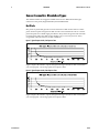
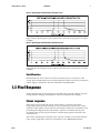
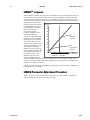
1M28-SA
1M75-SA
One Megapixel CMOS Stop Action Camera Family
Camera User’s Manual
03-32-00525 rev 03
Printed 06/12/03 4:43 PM
2
PRELIMINARY
1M28 and 1M75 User’s Manual
© 2003 DALSA. All information provided in this manual is believed to be accurate and reliable. No
responsibility is assumed by DALSA for its use. DALSA reserves the right to make changes to this
information without notice. Reproduction of this manual in whole or in part, by any means, is prohibited
without prior permission having been obtained from DALSA.
About DALSA
DALSA is an international high performance semiconductor and electronics company that designs,
develops, manufactures, and markets digital imaging products and solutions, in addition to providing
wafer foundry services. DALSA’s core competencies are in specialized integrated circuit and electronics
technology, and highly engineered semiconductor wafer processing. Products include image sensor
components; electronic digital cameras; and semiconductor wafer foundry services for use in MEMS,
power semiconductors, image sensors and mixed signal CMOS chips.
DALSA is a public company listed on the Toronto Stock Exchange under the symbol “DSA”. Based in
Waterloo, On. Canada, the company has operations in Bromont, PQ; Colorado Springs, CO; Tucson, AZ;
Eindhoven, NL; Munich, Germany and Tokyo, Japan.
All DALSA products are manufactured using the latest state-of-the-art equipment to ensure product
reliability. All electronic modules and cameras are subjected to a 24 hour burn-in test.
For further information not included in this manual, or for information on DALSA’s extensive line of
image sensing products, please call:
DALSA Sales Offices
Waterloo
605 McMurray Rd
Waterloo, ON N2V 2E9
Canada
Tel: 519 886 6000
Fax: 519 886 8023
www.dalsa.com
[email protected]
Waterloo
Europe
Asia Pacific
605 McMurray Rd
Waterloo, ON N2V 2E9
Canada
Tel: 519 886 6000
Fax: 519 886 8023
www.dalsa.com
[email protected]
Breslauer Str. 34
D-82194 Gröbenzell
(Munich)
Germany
Tel: +49 - 8142 –
46770
Fax: +49 - 8142 –
467746
www.dalsa.com
[email protected]
Space G1 Building, 4F
2-40-2 Ikebukuro
Toshima-ku, Tokyo
171-0014
Japan
+81 3 5960 6353
(phone)
+81 3 5960 6354
(fax)
www.dalsa.com
[email protected]
DALSA Worldwide Operations
Colorado
Tucson
Europe
Springs
5055 Corporate Plaza
Drive
Colorado Springs, CO
80919
USA
Tel: 719 599 7700
Fax: 719 599 7775
www.dalsa.com
[email protected]
3450 S. Broadmont Dr.
Suite #128
Tucson, AZ 857135245
USA
Tel: 520 791 7700
Fax: 520 791 7766
http://lifesciences.dalsa
.com
[email protected]
Breslauer Str. 34
D-82194 Gröbenzell
(Munich)
Germany
Tel: +49 - 8142 –
46770
Fax: +49 - 8142 –
467746
www.dalsa.com
[email protected]
Asia Pacific
Space G1 Building, 4F
2-40-2 Ikebukuro
Toshima-ku, Tokyo
171-0014
Japan
+81 3 5960 6353
(phone)
+81 3 5960 6354
(fax)
www.dalsa.com
[email protected]
Camera Link is a trademark registered by PULNiX America Inc., as chair of a committee of industry
members including DALSA.
03-32-00525-03
DALSA
1M28 and 1M75 User’s Manual
PRELIMINARY
3
Contents
Introduction to the 1M28 and 1M75 __________________________________________ 5
1.1 Camera Highlights .......................................................................................................................................................5
1.2 Image Sensor ...............................................................................................................................................................6
1.3 Pixel Response .............................................................................................................................................................9
1.4 Gain Response .............................................................................................................................................................12
1.5 Spectral Responsivity....................................................................................................................................................15
1.6 Region of Interest (ROI)...............................................................................................................................................15
1.7 Camera Performance Specifications.............................................................................................................................16
Camera Hardware Interface ________________________________________________ 19
2.1 Configuration ...............................................................................................................................................................19
2.2 Installation Overview ...................................................................................................................................................19
2.3 Input/Output ................................................................................................................................................................20
2.4 Default Settings............................................................................................................................................................20
2.5 Connectors....................................................................................................................................................................20
2.6 Power Supplies ............................................................................................................................................................22
2.7 Control Inputs, Camera Link ........................................................................................................................................22
2.8 Data Bus, Camera Link ................................................................................................................................................22
2.9 Timing..........................................................................................................................................................................23
2.10 Dummy Test Row .......................................................................................................................................................27
2.11 LED Status..................................................................................................................................................................27
Software Interface: Controlling the Camera _____________________________________ 29
3.1 Overview ......................................................................................................................................................................29
3.2 PFRemote Configuration Tool......................................................................................................................................30
3.3 Modifying Camera Registers ........................................................................................................................................32
3.4 Register Descriptions....................................................................................................................................................33
3.5 PFLIB API Commands..................................................................................................................................................40
Optical and Mechanical Considerations________________________________________ 41
4.1 Mechanical Interface ....................................................................................................................................................41
4.2 Optical Interface...........................................................................................................................................................42
4.3 Compliance...................................................................................................................................................................42
DALSA
03-32-00525-03
4
03-32-00525-03
PRELIMINARY
1M28 and 1M75 User’s Manual
DALSA
1M28 and 1M75 User’s Manual
PRELIMINARY
5
1
Introduction to the 1M28
and 1M75
1.1 Camera Highlights
Features
•
“Stop Action” (SA) imaging.
•
Exposure control.
•
1-Megapixel (1024 x 1024) resolution.
•
Up to 75 frames per second (fps).
•
CMOS image sensor.
•
LINLOG™ output response.
•
Windowing capability for increased frame rates.
•
CE compliant, shock and vibration tested.
•
Single 5V power supply input.
•
Robust and compact.
Programmability
DALSA
•
Programmable features include: gain, offset, line rates, trigger mode, test pattern
output, and camera diagnostics.
•
DLLs for integrating camera control functions into your system. The DLLs require a
framegrabber that has a virtual COM port, or a COM port input.
03-32-00525-03
6
PRELIMINARY
1M28 and 1M75 User’s Manual
Description
The 1M28 and 1M75 Cameras are based on a specially developed high-performance
CMOS image sensor, which enables high speed, global shutter technology for snap-shot
imaging, and award winning LINLOG technology for over 120dB of intrascene dynamic
range. The camera was developed for industrial vision applications targeting the best
today’s CMOS image sensor technology can offer. Special effort was put into the
development of a versatile, user-friendly, and robust camera.
Applications
The 1M28 and 1M75 are aimed at demanding applications in industrial image processing
and measurement and are ideal for applications with large illumination differences. Some
applications include:
•
Electronics manufacturing
•
Welding inspection
•
Traffic management
1.2 Image Sensor
The 1M28 and 1M75 cameras use a high-performance megapixel CMOS image sensor
capable of windowing and a dynamic range of 120dB.
Table 1: Sensor Characteristics
03-32-00525-03
Pixel number
1024 x 1024
Pixel size
10.6 x 10.6 µm
Full well capacity (Saturation)
200 000 electrons
Shutter Mode
Global, non-rolling
Min. Region of Interest (ROI)
4 rows x 1 column
Fill Factor
35% (diode area only)
Quantum Sensitivity
2µV/electron (8µV/electron with gain)
Inpixel programmable gain
~4x
Response
Linear, LINLOG , or logarithmic
Dynamic Range
48dB linear (8bit); 120dB LINLOG
Quantum Efficiency
25% (including fill factor)
TM,
Exposure Time
1 µs—0.5s in steps of 35ns
Sensitivity
10 µJ/m /LSB @630 nm, 8 bit
Spectral Range
400 - 800nm
TM
2
Number of outputs
1 or 4
Dimensions
55 mm (B) x 55 mm (H) x 50 mm (L)
Weight
200g
DALSA
1M28 and 1M75 User’s Manual
PRELIMINARY
Table 2: Cosmetic Specifications for the 1M28 and 1M75
Blemish Specification
7
Value
A
Number of first and last columns excluded
4
B
Number of first and last rows excluded
4
C
Blemish pixel deviation from average output under
illumination
over 30DN and under
20DN
D
Blemish pixel deviation from average dark level, measured
at dark
over 30DN
E
Maximum number of bright single pixel blemishes at dark
300
F
Maximum number of bright single pixel blemishes under
illumination
225
G
Maximum number of dark single pixel blemishes under
illumination
40
H
Maximum number of bright clusters at dark
10
I
Maximum number of bright clusters under illumination
2
J
Maximum number of dark clusters under illumination
10
K
Maximum size of bright clusters at dark
2
L
Maximum size of bright clusters under illumination
2
M
Maximum size of dark clusters under illumination
6
Notes:
DALSA
1.
Blemishes are measured over an entire frame of data and counted within the frame
boundaries defined by A and B above.
2.
Single pixel blemishes are defined as a pixel with an output as defined in C and D. A
bright single pixel defect occurs when the pixel exceeds the average output as defined
in C and a dark single pixel defect occurs when the pixel is below the average output
as defined in C.
3.
Clusters are a group of adjacent blemishes.
4.
Illumination analysis done at half saturation: the average pixel output of all pixels
within the frame is 128DN.
5.
All tests conducted with gain off and skimming off with QTH lamp (color temp.
3200K) with Wide Band Hot Mirror (750nm cutoff).
6.
Exposure time set to 10ms.
7.
Camera operating in linear mode.
8.
Camera operating under 25°C ambient temperature.
03-32-00525-03
8
PRELIMINARY
1M28 and 1M75 User’s Manual
Sensor Cosmetics: Blemishes Types
The 1M28 and 1M75 one megapixel CMOS sensor has two different blemish types,
referred to as hot pixels (bright blemishes) and dark blemishes.
Hot Pixels
Hot pixels are pixels that generate excessive amounts of dark current relative to other
pixels. Some hot pixels will generate dark current at 10 to 20 times the rate of a normal
pixel. Hot pixels are isolated single pixel defects. They follow the general rule of thumb
for dark current where the dark current doubles every 7-8°C. They are more easily
recognizable when the camera is in dark conditions.
Figure 1: Typical Output at Dark, 1ms Exposure Time
Figure 1 depicts the number of pixels that generate larger amounts of dark current than
your average pixel—the average pixel level output is 7DN.
Figure 2: Typical Output at Dark, 10ms Exposure Time
Figure 2 depicts the number of pixels that generate larger amounts of dark current than
your average pixel—the average pixel level output is 8DN.
03-32-00525-03
DALSA
1M28 and 1M75 User’s Manual
PRELIMINARY
9
Figure 3: Typical Output at Half Saturation, 1ms Exposure Time
Figure 3 depicts the histogram of pixel output values when the average pixel level output
is 128DN.
Figure 4: Typical Output at Half Saturation, 10ms Exposure Time
Figure 4 depicts the histogram of pixel output values when the average pixel level output
is 128DN.
Dark Blemishes
Dark blemishes are areas of the sensor where the pixel(s) are not as responsive as the
average pixel. Dark blemishes can be isolated single pixel defects, but can also be found in
clusters. Figure 3 and Figure 4 show the distribution of dark blemishes.
1.3 Pixel Response
Three principal modes of pixel response are possible: Linear response, LINLOG response
for high dynamic imaging, and logarithmic response for high dynamic imaging.
Linear response
In the linear response mode, the camera works similar to a classical CCD camera,
integrating the photo-generated charges in each pixel during the exposure time. In this
mode the output signal is a linear function of the number of photons accumulated in each
pixel during the integration time. If the number of photons accumulated in one pixel
exceeds the pixel capacity, the pixel saturates, and the output signal is truncated to the
maximum level.
This mode is advantageous if linearity of the response is needed over the whole dynamic
range, and for applications with intra scene dynamics up to 40dB-60dB amplitude.
DALSA
03-32-00525-03
10
PRELIMINARY
1M28 and 1M75 User’s Manual
LINLOGTM response
In the LINLOG mode the pixel response can be influenced to prevent pixel saturation. At
low intensities, each pixel has a linear response. Once a threshold of charge collected is
reached, the pixel changes its response to a logarithmic compression. This prevents the
saturation of the pixel response and permits an extremely high intra scene dynamic above
120dB. The threshold when
the pixel passes from a linear
Response
20
to a logarithmic response is
18
programmable by software.
Special care has been
16
invested to keep this
transition continuous and
14
smooth. The LINLOG
TM
12
LINLOG
response is compatible with
response
the global shutter technique
10
(all pixels are exposed at the
8
same time) which prevents
motion artefacts known from
6
classical logarithmic sensors.
4
The LINLOG technology
Logarithmic
further overcomes image lag,
2
response
or ghost images related to the
0
slow response speed of pure
logarithmic sensors. The
0
5
10
15
20
Intensity25
TM
LINLOG response is best
LINLOG Transition
suited for application with
uncontrolled illumination conditions or high intrascene contrasts where a high pixel
response is needed. Welding and traffic management are two application examples best
suited for the LINLOG response.
LINLOG values are set using the PFRemote configuration tool. See section 3.2 PFRemote
Configuration Tool for details.
LINLOG Parameter Adjustment Procedure
There is no direct formula for the interactions of LL1, LL2, and COMP. To determine
optimal settings, use the flowchart on the next page.
03-32-00525-03
DALSA
1M28 and 1M75 User’s Manual
PRELIMINARY
11
Figure 5: LINLOG Parameter Adjustment Procedure
START
Take a picture
Analyze the
overexposed areas
LL1 = 0000h
LL2 = 0000h
TIME = 0
Rough settings LL1
Phase 1
Initial value LL1 = 62.5
Take a picture
decrease
LL1
Find the center of gravity
of the histogram of the
overexposed areas
Gray scale 160 <
Center of
gravity of
histogram
increase
LL1
< Gray scale 200
Phase 2
Rough setting for COMP
Initial value = 5
Take a picture
increase
COMP
decrease
COMP
too low
Is the contrast in the
overexposed areas acceptable ?
too high
Yes
Phase 3
DALSA
03-32-00525-03
12
PRELIMINARY
1M28 and 1M75 User’s Manual
Rough settings for LL2
Initial value LL2 = 37.5
Phase 3
LL2 < LL1
Take a picture
decrease
LL2
too high
increase
LL2
Is the contrast in the
overexposed areas acceptable ?
too low
Yes
Black adjust
Phase 4
Fine adjustment of
LL1
LL2
COMP
Black adjust
Phase 5
Adjustment of
characteristics using LUT,
optimized for the
application's gray scale
output: 8 Bit
END
1.4 Gain Response
The cameras feature two gain options: Camera Gain and Skimming Gain.
03-32-00525-03
DALSA
1M28 and 1M75 User’s Manual
PRELIMINARY
13
Camera Gain (Highgain)
A preprogrammed off-chip amplification of either 1x or 4x gain before AD conversion can
be applied. This gain allows one to get more information out of sparsely illuminated
scenes, or increases the spread of gray levels when using strong logarithmic compression.
Skimming Gain
This gain can amplify small signal levels before readout, thereby increasing sensitivity
before readout noise adds to the signal. Due to the thermally generated leakage current,
this gain is only suitable for relatively short exposure times since it significantly increases
the FPN created by thermal current. The skimming gain can be combined with LINLOG
response, though the LINLOG transition parameters have to be chosen carefully to
prevent blackout of the sensor. The skimming gain should not be used with very short
frame periods, since it has a slightly increased time constant.
Both gains can be combined, though this increases FPN significantly and usually requires
you to recalibrate the black level.
Figure 6: Skimming and Camera Gain
Camera
Sensor
Signal
Skimming Gain
1x or 4x
Camera Gain
1x or 4x
Note: In skimming mode increased responsivity results in a nonlinear output.
Note: Gain values are set using the PFRemote configuration tool. See section 3.2
PFRemote Configuration Tool for details.
DALSA
03-32-00525-03
14
PRELIMINARY
1M28 and 1M75 User’s Manual
Figure 7: Camera Output Performance Skimming On vs. Skimming Off
Tint = 10ms λ = 626nm
250
Greyscale
200
150
100
No skimming
50
Skimming on
0
0.00E+00
1.00E-05
2.00E-05
3.00E-05
4.00E-05
Intensity [W/cm2]
Figure 8: Highlight of Low Intensity Values
Tint = 10ms λ = 626nm Zoom in
180
160
Greyscale
140
120
No skimming
100
Skimming on
80
60
40
20
0
0.00E+00
1.00E-06
2.00E-06
3.00E-06
4.00E-06
5.00E-06
I [W/cm2]
03-32-00525-03
DALSA
1M28 and 1M75 User’s Manual
PRELIMINARY
15
1.5 Spectral Responsivity
Figure 9: 1M28-SA and 1M75-SA Spectral Responsivity
The cameras are shipped without any filters. The quantum response is only limited by the
physics of silicon in manufacturing technologies. This permits applications in the near UV
as well as in the IR Band. For classical visible applications, consider the use of IR stop
filters to increase the sharpness of the images since commercial lenses often cannot
provide proper focalization over such a large spectrum.
Note: Although not shown, the cameras are responsive to light from 380 to 1100nm.
1.6 Region of Interest (ROI)
Note: To set the ROI,
refer to Chapter 3.
Software Interface:
Controlling the Camera.
The CMOS sensor allows you access to subregions of the pixel matrix through the region
of interest function. The benefit of limiting the region of interest is the resulting increase
in frame rate.
In Y direction the ROI can be placed arbitrarily, and can be as small as a single line. The
frame rate increases linearly with a reduction in lines read out.
In X direction the ROI must include at least 4 columns for the 1M28 camera and at least 8
columns for the 1M75. If this condition is respected, the speed increase in column
direction is also linear to the reduction in read out columns.
Theoretically, the smallest ROI is 4 columns x 1 row for the 1M28, and 8 columns x 1 row
for the 1M75.
Table 3: Max Frame Rate versus Resolution (Exposure Time = 10µs)
ROI Dimension (col x line) 1M28
1M75
DALSA
512 x 512
105 Fps
286 Fps
256 x 256
411 Fps
1070 Fps
128 x 128
1587 Fps
3700 Fps
128 x 16
11111 Fps
22000 Fps
03-32-00525-03
16
PRELIMINARY
1M28 and 1M75 User’s Manual
ROI Dimension (col x line) 1M28
1M75
1024 x 1
37000 Fps
20000 Fps
1.7 Camera Performance Specifications
Table 4: 1M28 an 1M75 Performance Specifications
Physical Characteristics
Units
Power Dissipation, typ
W
2
Time to power up, typ
sec.
5
Data output format
bits
8 and 10
µm
mm
°
±300
±0.10
±0.5
Operating Ranges
Units
Min
(1M28
and
1M75)
Data Rate, Internal MCLK
MHz
Sensor Alignment
x, y
z
0z
External MCLK
Camera Link™
2
Max
(1M28)
Max
(1M75)
Notes
28.375
40
MHz
20 (1M28)
10 (1M75)
28.375
20
Temperature
°C
0
40
40
1
Frame Rate
Units
Min
Max
(1M28)
Max
(1M75)
Notes
Full resolution (1024 x 1024)
fps
1
27
75
With windowing
fps
>100,000
>100,000
Electro-Optic
Specifications
Units
Gain
Value
Description
Average
Broadband
Responsivity, typ
DN/(nJ/
2
cm )
1x
0.7
Skimming off, Gain
off
~4x
2.8
Skimming on, Gain
off
4x
2.8
Skimming off, Gain
on
~16x
11.2
Skimming on, Gain
on
1x
490:1
Skimming off, Gain
off
~4x
350:1
Skimming on, Gain
off
4x
350:1
Skimming off, Gain
on
Dynamic Range
(rms), max
03-32-00525-03
Notes
Ratio
Notes
DALSA
1M28 and 1M75 User’s Manual
PRELIMINARY
Electro-Optic
Specifications
RMS Noise, max
FPN (rms), max
PRNU (rms), max
DC Offset
Units
DN
DN
DN
17
Gain
Value
Description
~16x
196:1
Skimming on, Gain
on
1x
0.5
Skimming off, Gain
off
~4x
0.7
Skimming on, Gain
off
4x
0.7
Skimming off, Gain
on
~16x
1.25
Skimming on, Gain
on
1x
3.0
Skimming off, Gain
off
~4x
5.0
Skimming on, Gain
off
4x
8.5
Skimming off, Gain
on
~16x
11.0
Skimming on, Gain
on
1x
2.5
Skimming off, Gain
off
~4x
5.0
Skimming on, Gain
off
4x
15.0
Skimming off, Gain
on
~16x
15.0
Skimming on, Gain
on
DN
Power Supply Current Vin @ 5V
Notes
Programmable
Units
Typ
Max
mA
310
400
Regulatory Compliance
Value
CE compliance
EN 61000-6-3 : 2001
EN 61000-6-2 : 2001
Shock & Vibration Immunity
IEC/EN 60068-2-6
IEC/EN 60068-2-27
Notes:
DN = Digital Numbers (0-255); also known as gray levels.
All measurements taken in 8-bit linear output mode.
All specifications are valid for the front plate temperature range of 0°C to 40°C, in still air.
DALSA
1.
Measured at front plate.
2.
10 bit output available with the 1M28 only.
03-32-00525-03
18
03-32-00525-03
PRELIMINARY
1M28 and 1M75 User’s Manual
DALSA
1M28 and 1M75 User’s Manual
PRELIMINARY
19
2
Camera Hardware
Interface
2.1 Configuration
The different modes of operation and settings are programmed in the camera by an
asynchronous serial communications available through the Camera Link interface. The
serial interface operates at 9600 baud. The default values are stored in an EEPROM, which
is automatically read at power up. The user can change the factory settings of the default
values in the EEPROM to configure the camera to the requirements of their own
application. You can also save the set of default values to a file over the asynchronous
serial communications interface, or restore default settings saved in a file to the EEPROM.
The configuration is most easily done with the PFRemote configuration tool shipped with
the camera. The PFRemote tool is explained in section 3.2 PFRemote Configuration Tool
on page 30.
2.2 Installation Overview
In order to set up your camera, you should take these steps:
1. Connect Camera Link™ cables from camera to framegrabber.
2. Connect power.
You must also set up the other components of your system, including light sources,
framegrabbers, camera mounts, heat sinks, host computers, optics, encoders, and so on.
See section 2.1 above for camera configuration information.
DALSA
03-32-00525-03
20
PRELIMINARY
1M28 and 1M75 User’s Manual
2.3 Input/Output
+5V and Ground
Diagnostic LED
Camera Link™
!
WARNING: It is extremely important that you apply the appropriate voltages to your
camera. Incorrect voltages will damage the camera.
2.4 Default Settings
The camera power-ups for the first time with the following default settings.
Table 5: Default Settings
Specifications
1M28
1M75
EXSYNC
Internal, free-running
Internal, free-running
Data output
8-bits
8-bits
Output response
Linear
Linear
Gain
1x
1x
Resolution
Full-resolution, 1024 x 1024
Full-resolution, 1024 x 1024
Exposure time
10 ms
12 ms
Frame rate
20 fps
25 fps
Data rate
28MHz
2x40MHz
2.5 Connectors
Please refer to the Camera Link standard for detailed information on signal levels and
timings.
Table 6: Pinout of the MDR26 camera connector for the Camera Link interface
Camera Link Cable
Base Configuration
One Channel Link Chip + Camera Control + Serial Communication
03-32-00525-03
Camera Connector
Right Angle Framegrabber Channel Link Signal
1
1
inner shield
14
14
inner shield
2
25
X0-
DALSA
1M28 and 1M75 User’s Manual
PRELIMINARY
21
Camera Link Cable
Base Configuration
One Channel Link Chip + Camera Control + Serial Communication
Camera Connector
Right Angle Framegrabber Channel Link Signal
15
12
X0+
3
24
X1-
16
11
X1+
4
23
X2-
17
10
X2+
5
22
Xclk-
18
9
Xclk+
6
21
X3-
19
8
X3+
7
20
SerTC+
20
7
SerTC-
8
19
SerTFG-
21
6
SerTFG+
9
18
CC1-
22
5
CC1+
10
17
CC2+
23
4
CC2-
11
16
CC3-
24
3
CC4+
12
15
inner shield
25
2
inner shield
Table 7: DALSA Camera Control Configuration
Signal Configuration
Pin
CC1
EXSYNC
9, 22
CC2
External Master Clock
10, 23
CC3
PRIN (Exposure Control)
11, 24
CC4
Not Used
12, 25
Table 8: Pinout of the Binder712
PIN I/O Name Meaning
1
PW
VDD
+5V power supply
2
PW
GND
ground
3
PW
VDD2
Not used
3
1
2
DALSA
03-32-00525-03
22
PRELIMINARY
1M28 and 1M75 User’s Manual
2.6 Power Supplies
The camera requires a single voltage input (+5V). The camera meets all performance
specifications using standard switching power supplies, although well-regulated linear
supplies provide optimum performance. See section 1.7 Camera Performance
Specifications for current requirements.
When setting up the camera’s power supplies follow these guidelines:
!
•
Protect the camera with a fast-blow fuse between power supply and camera.
•
Do not use the shield on a multi-conductor cable for ground.
•
Keep leads as short as possible to reduce voltage drop.
WARNING: It is extremely important that you apply the appropriate voltages to your
camera. Incorrect voltages will damage the camera. Protect the camera with a fast-blow
fuse between power supply and camera.
2.7 Control Inputs, Camera Link
The camera accepts control inputs through the Camera Link MDR26F connector. All
inputs are optional. The camera ships in free-running mode. Refer to section 3 for more
information on setting frame rates and exposure times and camera modes.
EXSYNC (Triggers Frame Readout)
EXSYNC is an optional input signal that can be used to trigger the line readout rate. This
camera uses the rising edge of EXSYNC to trigger line readout.
IMPORTANT:
This camera uses the rising
edge of EXSYNC to trigger
line readout, unlike
previous DALSA cameras,
which used the falling edge.
Note: EXSYNC should not be clocked faster than the camera’s specified maximum frame
rate. When the constant frame rate register is enabled (default setting), the camera ignores
the EXSYNC pulse until it has completed reading the last frame out. If the constant frame
rate is disabled, the EXSYNC pulse will start integration even if the camera has not read
out all the pixels in the frame. Refer to section 3.8 Register Descriptions for more
information.
External MCLK
External MCLK is an optional signal used to control the data rate.
PRIN
PRIN is an optional input signal used for exposure control (PRIN).
2.8 Data Bus, Camera Link
These signals indicate when data is valid, allowing the data to be clocked from the camera
to your acquisition system. These signals are part of the Camera Link configuration. Refer
to the DALSA Camera Link Implementation Road Map, available at
http://vfm.dalsa.com, for the standard location of these signals:
03-32-00525-03
DALSA
1M28 and 1M75 User’s Manual
PRELIMINARY
23
Clocking Signal
Indicates
FVAL (high)
LVAL (high)
DVAL (high)
STROBE (rising edge)
Outputting valid frame
Outputting valid line
Valid data
Valid data
Digital Data
The 1M28 digitizes internally to 10 bits and outputs either all 10 bits or the most
significant 8 bits on the Camera Link connector. The 1M75 only outputs the most
significant 8 bits.
2.9 Timing
The cameras feature many possibilities for flexible timing. In free running mode, the
camera delivers, independently of external signals, data according to the timing settings
in the internal registers. In triggered mode, the camera starts integration after an external
trigger pulse. During integration and readout all further trigger pulses are ignored. The
maximum rate at which the camera accepts external triggers is defined by the frame
timer. The minimum exposure time, for any operating mode, is 560 ns.
Frame Timer
The frame timer is used to fix the frame rate of the camera in free running mode or to set
the maximum rate at which the camera accepts external triggers. In order to obtain the
maximum frame rate, the frame timer must be set as close to the sum of the readout time,
exposure time, and reset time as possible. This is especially important if the frame rate is
to be increased by windowing. Note: The reset time is small, at 1-2µs.
Figure 10: External Trigger Mode, Constant Image Data Rate
Ignored
Exsync
Exsync
Integration
Readout
Reset
Integration
Frame Timer
Figure 11: External Trigger Mode, Variable Image Data Rate
Integration
DALSA
Readout
Reset
Integration
03-32-00525-03
24
PRELIMINARY
1M28 and 1M75 User’s Manual
Figure 12: Free Running Mode, Constant Image Data Rate
Integration
Readout
Reset
Integration
Frame Timer
Figure 13: Free Running Mode, Variable Image Data Rate
Integration
Readout
Integration
Readout
Global Shutter Timing
With a global shutter, the sensor starts with a global reset of all pixels. Then during the
integration time, photo-generated electrons are collected in the pixels. After the exposure
time, the collected electrons are transferred to a storage node, and sequential readout of
the sensor matrix begins. As a result, all pixels are exposed to light for the same amount
of time, resulting in crisp images that do not suffer from the time displacement artefacts
characteristic of rolling shutter CMOS cameras.
Figure 14: Global Shutter Timing
Reset
Integration
Frame Readout
Data
Global shutter
Reset
Freerunning Mode
The freerunning mode is the factory set timing mode at power up and captures images
without the need for an external control signal. The sensor data is read out after the set
integration time. After the sensor is finished reading out, the sensor resets and the
sequence begins again. The date is output on the rising edge of the pixel clock.
The signals FRAME_VALID (FVAL) and LINE_VALID (LVAL) mask valid image
information. The number of clock pixels after exposure CPRE is defined by the calculation
of the frame time
03-32-00525-03
DALSA
1M28 and 1M75 User’s Manual
PRELIMINARY
25
Figure 15: Freerunning Mode
PCLK
Frametimer
Integration
CPRE
FVAL
Line Pause
First Line
Line Pause
Last Line
Line Pause
LVAL
DATA
Note: To set integration mode and parameters, refer to Chapter 3. Software Interface:
Controlling the Camera.
Triggered Mode
In triggered mode, image aquistition begins with the rising edge of an external trigger
pulse. The image is read out after the preset exposure time. After readout, the sensor
resets and the camera waits for a new trigger pulse. The data is output on the rising edge
of the pixel clock.
The signals FRAME_VALID (FVAL) and LINE_VALID (LVAL) mask valid image
information. The number of clock pulses after exposure CPRE is defined by the
calculation of the frame time.
Figure 16: Triggered Mode
PCLK
EXSYNC
EXSYNC is ignored in mode constant image data rate
INTEGRATION
CPRE
FVAL
Line Pause
First Line
Line Pause
Last Line
Line Pause
LVAL
DATA
Triggered Mode with External Exposure Control
In triggered mode with external exposure control, sensor control is reset with the rising
edge of an external trigger pulse. The exposure of the image is controlled by the external
signal PRIN. The sensor control is clocked in such a way that that the image exposure
becomes active one clock later. The image is read out after the exposure time has elapsed.
DALSA
03-32-00525-03
26
PRELIMINARY
1M28 and 1M75 User’s Manual
After readout, the sensor returns to the reset state and the camera waits for a new trigger
pulse.
The data is output on the rising edge of the pixel clock. The signals FRAME_VALID
(FVAL) and LINE_VALID (LVAL) mask valid image information. The signal
INTEGRATION indicates the active integration phase of the sensor. The number of clock
pulses after exposure CPRE is defined by the calculation of the frame time.
Figure 17: Trigger Mode with External Exposure Control Timing Diagram
PCLK
EXSYNC
EXSYNC is ignored in mode constant image data rate
PRIN
INTEGRATION
CPRE
FVAL
Line Pause
First Line
Line Pause
Last Line
Line Pause
LVAL
DATA
Triggered Mode with External Edge Triggered
Exposure Control
In triggered mode with external edge exposure control, sensor control is reset with the
rising edge of an eternal trigger pulse, after which exposure of the image begins. The
integration ends with the rising edge of the external signal PRIN. The signals EXSYNC
and PRIN are clocked in the sensor control in such a way that the internal exposure
control becomes active one clock later.
The image is read out after the exposure time has elapsed. After readout, the sensor
returns to the reset state and the camera waits for a new trigger pulse.
The data is output on the rising edge of the pixel clock. The signals FRAME_VALID
(FVAL) and LINE_VALID (LVAL) mask valid image information. The signal
INTEGRATION indicates the active integration phase of the sensor. The number of clock
pulses after exposure CPRE is defined by the calculation of the frame time.
03-32-00525-03
DALSA
1M28 and 1M75 User’s Manual
PRELIMINARY
27
Figure 18: Triggered Mode with External Edge Triggered Exposure Control
PCLK
EXSYNC
EXSYNC is ignored in mode constant image data rate
PRIN
INTEGRATION
CPRE
FVAL
Line Pause
First Line
Line Pause
Last Line
Line Pause
LVAL
DATA
2.10 Dummy Test Row
For testing the readout chain a row of test pixels has been implemented on the sensor
chip. The pixels in this row are fixed to a pattern of black and white pixels. This row can
be read out in place of row 1023, at the beginning of the frame. Note: The camera powers
up with the dummy test row turned off. For information on turning the dummy test row
on , refer to Table 14 on page 37.
2.11 LED Status
A status LED on the backside of the camera provides the following information about the
state of the camera:
DALSA
•
In normal operation mode, the LED shows a green light while valid data is read out.
•
At slow frame rates the LED blinks with the FVAL signal.
•
At high frame rates the LED changes to an apparently continuous green light, with
intensity proportional to the ratio of readout time over frame time. In some
circumstances, (for example, a relatively long frame time and a very small ROI
setting) the pulse of the LED might be too short to be visible in daylight conditions,
even if the camera is working properly.
•
If the data read out from the sensor is not within the ADC conversion range (over or
under exposed), the LED changes to red while the saturated data is read out.
•
The status LED changes to red while the serial communication is active.
03-32-00525-03
28
03-32-00525-03
PRELIMINARY
1M28 and 1M75 User’s Manual
DALSA
1M28 and 1M75 User’s Manual
PRELIMINARY
29
3
Software Interface:
Controlling the Camera
3.1 Overview
Many camera features can be controlled through the serial interface. The camera can also
be used without the serial interface after it has been set up correctly.
To configure the camera through the serial interface, you must use the PFRemote
configuration tool. For details on using the PFRemote, refer to section 3.2 PFRemote
Configuration Tool on page 30.
You can also configure the camera through the PFLIB application programming interface.
For more information, refer to section 3.5 PFLIB API Commands on page 40.
Camera Serial Port Defaults
DALSA
•
8 data bits
•
1 start bit
•
1 stop bit
•
No parity
•
9.6Kbps
03-32-00525-03
30
PRELIMINARY
1M28 and 1M75 User’s Manual
3.2 PFRemote Configuration Tool
The pfremote.exe is a remote configuration tool for the 1M28 and 1M75 cameras. With the
PFRemote, you can:
•
Control basic camera functions, such as gain, frame rates, and exposure times
•
Set exposure time
•
Set a window of interest
•
Set LinLog parameters
•
Set camera skimming
•
Read and alter camera registers
•
Save factory settings to your local computer
Install PFRemote
A 1M28_1M75_PFRemote_Software.zip file is provided on the CD shipped with the
camera. Unzip the 1M28_1M75_PFRemote_Software.zip and copy the files contained in
the zip file to a directory on your computer. Alternately, the latest version of the software
is also available at http://vfm.dalsa.com/docs/docs.asp in the “Software” folder.
Opening PFRemote
i
For further details
on using the
PFRemote and how
to configure the
camera, refer to the
help file.
To open the help
file:
1. On the Help
menu, click Help.
Alternately, you can
press F1.
03-32-00525-03
Before running PFRemote, make sure that you have installed your framegrabber and
framegrabber software.
To begin using the PFRemote:
1.
If it is not already open, open your framegrabber software with the configuration for
the 1M28 or 1M75 camera.
In the PFRemote folder:
1.
Double-click PFRemote.exe.
In the PFRemote dialog box:
2.
Right click on the COM port that the camera is connected to and select Open.
Figure 19: Opening a Camera with PFRemote
DALSA
1M28 and 1M75 User’s Manual
PRELIMINARY
31
If the camera is properly connected, the camera you are using is displayed:
Figure 20: Camera Name is displayed after a Successful Connection
If the camera is not connected properly, you will receive an error message. Consult
the troubleshooting section in the PFRemote Help for possible solutions.
Saving and Loading EEPROM Settings
!
IMPORTANT: If you are using PFRemote for the first time, you should dump the EEPROM in order
to save the current factory settings. This will enable you to recover the factory settings if they are
accidentally overwritten.
To save the factory settings:
1.
Select Tools → Dump EEPROM.
2.
Locate where you want to save the HEX file, enter a file name, and click Save.
To recover EEPROM settings:
1.
Select Tools → EEPROM Recovery.
2.
Locate the HEX file to upload and select Open.
3.
After the camera has completed uploading the file, shut down and then restart your
camera.
Configuring the Camera with PFRemote
To configure the camera:
DALSA
1.
In PFRemote, open a connection with the camera. For details on opening a connection
with your camera, see Opening PFRemote on page 30.
2.
Right click on the camera name and select Configure.
03-32-00525-03
32
PRELIMINARY
1M28 and 1M75 User’s Manual
The configuration dialog box opens:
3.
Depending on what you want to configure, click the appropriate tab and begin
camera configuration.
The PFRemote Help file explains each dialog box in detail. To access the help file, select
Help → Help, or click F1.
3.3 Modifying Camera Registers
The camera modes and functions are set and stored by internal camera registers. The
internal registers are initialized during power-up or by the software. During power-up,
the contents of the EEPROM are copied to the registers, after which, the camera is ready
to use.
The camera is factory-preset to operate in free-running mode with an 8-bit resolution and
a linear response. The corresponding values in each camera may be different from the
factory values due to the fine-tuning of each module.
!
To avoid problems with modified presets and to ensure the restoration of original
values, we recommend that you save the factory presets to an external storage media. To
save and restore the values, use the PFRemote.exe. Refer to Saving and Loading
EEPROM Settings on page 31 for further information on the PFRemote.
We also recommend that you do not alter the custom calibration settings available
through the calibration dialog box (Camera → Calibration). Consult DALSA support at
[email protected] before altering calibration values.
The basic settings of the camera can be modified and stored (in the EEPROM) by the user.
The user can modify all parameters via the PFRemote software interface. After testing the
new parameters, they can be stored in the EEPROM. We recommend that you store your
parameters in the same way as the factory presets.
To modify camera registers:
1.
03-32-00525-03
In PFRemote, open a connection with the camera. For details on opening a connection
with your camera, see Opening PFRemote on page 30.
DALSA
1M28 and 1M75 User’s Manual
PRELIMINARY
33
2.
Select Camera → Registers. The Registers dialog box opens:
3.
In the left text boxes, enter the register values you wish to view.
4.
Click Reread all.
The current register values are displayed in the right text boxes.
5.
In the right text box, change the current value to the new value and click Change.
The register is now set to the new value. To verify the new settings, click Reread all. See
the following section for register descriptions.
3.4 Register Descriptions
Table 9: Sensor control registers, address 0 to 63
REG
REG
Read (R) /
Decimal
Hexadecimal Write (W)
Value
Value
or Command
(C)
DALSA
Description
0
0
R/W
Data EEPROM
1
1
W
LSB address EEPROM
2
2
W
MSB address and OP-Code
EEPROM
3
3
C
Command SEND_PROM, content of
registers 0 – 2 are sent to the
EEPROM
4
4
C/R
Command RELOAD of the registers
/ Status register has 3 internal states
5
5
R/W
Status register 4 internal states
6
6
R/W
Mode register 0 , adjust camera
modes
7
7
R/W
Mode register 1 , adjust camera
modes
8
8
W
LSB DAC
9
9
W
MSB DAC
03-32-00525-03
34
03-32-00525-03
PRELIMINARY
1M28 and 1M75 User’s Manual
REG
Decimal
Value
REG
Hexadecimal
Value
Read (R) /
Write (W)
or Command
(C)
Description
10
A
-
Not used
11
B
-
Not used
12
C
R/W
Mode register 2 , adjust camera
modes
13
D
R/W
Mode register 3 , adjust camera
modes
14
E
R/W
Mode register 4 , adjust camera
modes
15
F
R/W
LSB Exposure Time
16
10
R/W
MSB-1 Exposure Time
17
11
R/W
MSB Exposure Time
18
12
R/W
LSB LinLog Time
19
13
R/W
MSB-1 LinLog Time
20
14
R/W
MSB LinLog Time
21
15
R/W
LSB Frame pause
22
16
R/W
MSB-1 Frame pause
23
17
R/W
MSB Frame pause
24
18
R/W
LSB ROI-X0 boundary condition for
Region Of Interest (ROI) Sensor
matrix
25
19
R/W
MSB ROI-X0 boundary condition for
Region Of Interest (ROI) Sensor
matrix
26
1A
R/W
LSB ROI-Y0 boundary condition for
Region Of Interest (ROI) Sensor
matrix
27
1B
R/W
MSB ROI-Y0 boundary condition for
Region Of Interest (ROI) Sensor
matrix
28
1C
R/W
LSB ROI-X1 boundary condition for
Region Of Interest (ROI) Sensor
matrix
29
1D
R/W
MSB ROI-X1 boundary condition for
Region Of Interest (ROI) Sensor
matrix
30
1E
R/W
LSB ROI-Y1 boundary condition for
Region Of Interest (ROI) Sensor
matrix
31
1F
R/W
MSB ROI-Y1 boundary condition for
Region Of Interest (ROI) Sensor
matrix
32
20
R/W
Line pause
33
34-46
21
22-2E
R/W
Interlacing
Not Used
DALSA
1M28 and 1M75 User’s Manual
PRELIMINARY
35
REG
Decimal
Value
REG
Hexadecimal
Value
Read (R) /
Write (W)
or Command
(C)
Description
47
30
R/W
48
49
50
51
52
53
54
55
56
57
58
59
60
61
62
63
30
31
32
33
34
35
36
37
38
39
3A
3B
3C
3C
3E
3F
R/W
R/W
R/W
R/W
R/W
R/W
R/W
R/W
R/W
R/W
R/W
R/W
R/W
R/W
R/W
R/W
Choice of a RAM bank for
read/write access
Byte 0 of a 16x8 RAM-Bank
Byte 1 of a 16x8 RAM-Bank
Byte 2 of a 16x8 RAM-Bank
Byte 3 of a 16x8 RAM-Bank
Byte 4 of a 16x8 RAM-Bank
Byte 5 of a 16x8 RAM-Bank
Byte 6 of a 16x8 RAM-Bank
Byte 7 of a 16x8 RAM-Bank
Byte 8 of a 16x8 RAM-Bank
Byte 9 of a 16x8 RAM-Bank
Byte 10 of a 16x8 RAM-Bank
Byte 11 of a 16x8 RAM-Bank
Byte 12 of a 16x8 RAM-Bank
Byte 13 of a 16x8 RAM-Bank
Byte 14 of a 16x8 RAM-Bank
Byte 15 of a 16x8 RAM-Bank
Register address 00H – 03H (EEPROM control)
!
The first 4 registers are used to communicate with the EEPROM of the camera. See
Appendix C on page 49 for more information on these registers.
Register address 04H and 05H (Status registers)
The bits of status registers 3 (address 04H) and 4 (address 05H) contain status information
of sensor control registers. Status information of the sensor module can be read from
status register 3. Short-term error messages generated during camera operation (such as
asynchronous communications transmission error) are saved in status register 4. These
error flags can be reset by writing a logical 1 to the corresponding error bit.
Table 10 and Table 11 show the assignment of the registers.
Table 10: Status Register 3 (Register address REGADDR = 4D = 04H)
Register address 4 - STATUS3_REG
DALSA
Bit
Description
0
= 1 Ł AUTOLOAD, signals power-up or Reload of data (from EEPROM),
! No write operations to EEPROM allowed !
1
= 1 Ł PROM_BUSY, ! No write operations to EEPROM allowed !
2
always 0 Ł sensor module
3
=1 Ł ERROR_NO_EXSYNC, timeout digital mono flop
4
=1 Ł ERROR_NO_EXPOSURE, timeout digital mono flop
5
=1 Ł ERROR_NO_MCLK, timeout digital mono flop
6
Not used = 0
03-32-00525-03
36
PRELIMINARY
1M28 and 1M75 User’s Manual
Register address 4 - STATUS3_REG
Bit
Description
7
Not used = 0
Table 11: Status register 4 (Register address REGADDR = 5D = 05H)
Register address 5 - STATUS4_REG
Bit
Description
0
Error in the asynchronous communications transfer
1
CANCEL was active, i.e. read from non defined register
2
Not used = 0
3
Not used = 0
4
Not used = 0
5
Not used = 0
6
Not used = 0
7
Not used = 0
Register address 06H and 07H (Mode register 0 and 1)
Mode registers 0 and 1 control the basic functions of the camera. To ensure proper
operation, these registers are updated first during power-up. The functions of each
individual bit are shown in Tables 12, 13 and 14.
Table 12: Mode register 0 (Register address REGADDR = 6D = 06H)
Register address 6 - MODE0_REG
Bit
Name
Description
Default
0
ENABLE0
Camera on, = 1 Ł Camera in operation
1
1
ENABLE1
Invert Pixel Clock, = 1 Ł phase shift of 180
degrees
0
2
ENABLE2
0
3
ENABLE3
These bits are responsible for resolution, access
to the LUT’s and the LFSR interface test
4
EN_TOGGLE
= 1 Ł Automatic voltage switching active
1
5
EN_LL2_LOG
= 1 Ł LinLog2-response curve active
0
6
LOG
= 1 Ł Log response curve on
= 0 Ł Log response curve off
0
7
LINLOG
= 1 Ł LinLog-response curve on
= 0 Ł LinLog-response curve off
0
0
Table 13: Camera resolution and special functions
Enable3 Enable2 Function
Comment
03-32-00525-03
0
0
8 bit
Digital gain x 1
0
1
8 bit
LUT 10-to-8
Two user programmable LUT’s
LUT0 factory preset digital gain x 2
LUT1 factory preset digital gain x 4
1
0
10 bit
Digital gain x 1
1
1
10 bit LFSR
Interface test with Linear Feedback Shift
Register (LFSR)
DALSA
1M28 and 1M75 User’s Manual
PRELIMINARY
37
To test the interface reliability, a 10 bit Linear Feedback Shift Register (LFSR) is
implemented. A LFSR is a sequential shift register with combinational feedback logic
around it that causes it to pseudo-randomly cycle through a sequence of binary values. It
is reset at every line start. Thus it is possible to compare the incoming signal with an
internally generated one to count the transmission errors.
Table 14: Mode Register 1 (Register address REGADDR = 7D = 07H)
Register address 7 - MODE1_REG
!
Bit
Name
Description
Default
0 to 3
Reserved
Do not change
0
4
EN_DUMMY
= 1 Ł Dummy line on = 0 Ł Dummy line off
0
5
SKIM_IMAGE0
= 1 Ł Skim voltage 0 on, = 0 Ł Skim voltage 0 off 0
6
SKIM_IMAGE1
= 1 Ł Skim voltage 1 on, = 0 Ł Skim voltage 1 off 0
7
HIGH_GAIN
= 1 Ł Gain by 4, = 0 Ł gain by 1
0
WARNING: Do not modify Mode Register 1 (bits 0 to 3). If corruption occurs, write in default values or contact
DALSA. Modifying these values may result in a malfunction or limited functioning of the camera.
You should use the LSFR test pattern for data path integrity. Alternately, you can turn on
the dummy line. With the help of the dummy line, the transfer of data from the camera to
the framegrabber card can be easily tested.
When bits 5 to 7 are switched on (or off), a possible bias re-tuning of the video amplifier is
required. Typically this involves adjustment to the camera’s offset level.
Register address 08H and 09H (Interface DAC)
The registers 08H and 09H are used for the DAC access and for adjustments to the camera
in the various operating modes.
WARNING: Do not modify these values. An incorrect value can cause a malfunction of the camera!
Register address 0AH and 0BH
The registers 0AH and 0BH are NOT used.
Register address 0CH to 0EH (Mode register extended functions)
The registers 12 – 14 contain extended functions for camera adjustment.
Table 15: Mode register 2 (Register address REGADDR = 12D = 0CH)
Register address 12 - MODE2_REG
DALSA
Bit
Name
Description
Default
0
SYNC_EXTERN
= 1 Ł external synchronisation
0
1
CONST_FRAMERATE
= 1 Ł constant frame rate (in free running
mode)
1
2
FLIP_IMAGE
= 1 Ł output picture upside-down
0
3
EN_MROI
= 1 Ł Activate MROI Mode
0
4
EN_LINE_HOPPING
= 1 Ł Switch on line hopping
0
03-32-00525-03
38
PRELIMINARY
5
EN_ARBITRARY_LH
1M28 and 1M75 User’s Manual
= 1 Ł Switch on line hopping via LUT
0
6
EN_GLOBAL_RESET
= 1 Ł switch on global reset of the sensors
1
7
EN_MCLK
= 1 Ł activate external pixel clock
0
Table 16: Mode Register 3 (Register address REGADDR = 13D = 0DH)
Register address 13 - MODE3_REG
Bit
Name
Description
Default
0
EN_EXPOSURE_PW
External integration control (PulseWidth-Modulation) with EXPOSURE
signal
0
1
EN_EXPOSURE_FT
External integration control by edge
triggering EXSYNC and EXPOSURE,
integration begins on positive edge of
EXSYNC signal, integration ends on
positive edge of EXPOSURE signal
0
2
EN_SYNC_EXPOSURE
0
3
POLARITY_SYNC_EXPOSURE
4
EN_SHUTTER
5
EN_PRELOAD
External triggering and integration
control by EXPOSURE signal,
integration begins on positive edge of
EXPOSURE signal and EXSYNC is on,
integration ends on negative edge of
EXPOSURE Signal
= 1 Ł SYNC_EXPOSURE active HIGH
i.e. rising edge EXSYNC Signal =
EXSYNC and EXPOSURE on, falling
edge EXSYNC Signal = Exposure off
= 1 Ł SHUTTER Signal active, for
CameraLink standard set 0 Ł DVAL =
1
= 1 Ł Enable line preload
6
EN_LINE_RESET
= 1 Ł Enable line reset at the middle of
a line
0
7
Not Used
0
0
0
1
Table 17: Mode Register 4 (Register address REGADDR = 14D = 0EH)
Register address 14 - MODE4_REG
Bit
Name
Description
Default
0
SLAVE_ACTIVE
= 1 Ł Enable asynchronous serial
communications interface to ADC module
0
1 to 7
Not used
-
0
Registers 15-17 (exposure time)
The exposure time is stored in three (15 – 17) 8 bit registers (24 bits total).
The exposure time is set in increments of the pixel clock. For the 1M28, each increment is
35 ns. For the 1M75, each increment is 50 ns. The final exposure time can be calculated by
changing the stored binary value to a decimal value and multiplying by the time of the
appropriate increment for your camera.
03-32-00525-03
DALSA
1M28 and 1M75 User’s Manual
PRELIMINARY
39
Registers 18-20 (LinLog2)
The LinLog2 time constant is implemented as a 24 bit register (registers 18-20), similar to
the exposure time. The LinLog2 time constant must always be smaller than the exposure
time.
Registers 21-23 (Frame Time)
The frame time is set by registers 21-23. This value is set in increments of the pixel clock
(35ns for 1M28 and 50ns for 1M75). The frame time is used to keep the frame rate
constant, independent of the exposure time. NOTE: The frame rate sets the maximum
exposure time. Invalid values must be prevented via software.
Register 24-31 (ROI = Region Of Interest)
The registers 24-31 are used to define the region of interest of the sensor. The coordinates
of the corners of the ROI are written and take effect at the beginning of the next frame.
Invalid values must be prevented via software. Values x0>x1, or y0>y1, are ignored by the
camera. For full resolution:
x0, y0 = 0, 0
x1, y1 = 1023, 1023
Register 32 (Line pause)
This register stores the line pause value. It is also defined in increments of the pixel clock.
Valid line pause values are between 5 and 255. Default is 8.
Register 33: Line Jump (and Pixel Jump)
This register contains the value for the interlace mode. The line counter is incremented by
this value. The lines in between are skipped.
Register 47: RAM Bank Selection
The RAM banks in the FPGA are selected with this register.
Registers 48-63: Data for 16 x 8 RAM Banks
RAM banks have been implemented for internal parameters not used constantly by state
machines.
Frame Rate Calculation
To determine the frame rate, it is easiest to calculate the frame time first. The frame rate is
the inverse of frame time.
The frame time depends on the parameters exposure time, ROI, and line pause.
For the frame time:
DALSA
03-32-00525-03
40
PRELIMINARY
Frame time
1M28 and 1M75 User’s Manual
> exposure time + read out time
> exposure time + tU([No. of lines]*([No. of pixels]+Line pause)+ Line pause)
> exposure time + tU((ROI_Y1-ROI_Y0)*((ROI_X1-ROI_X0)+Line pause) + Line pause)
with the boundary conditions :
tU = Time unit in ns (35ns for 1M28 and 12.5ns for 1M75))
Line pause = 5 … 255
ROI_Y1-ROI_Y0 = max. 1024 lines
ROI_X1-ROI_X0 = max. 1024 pixels
3.5 PFLIB API Commands
The PFLIB application programming interface enables an application programmer to
control the 1M28 or 1M75 camera’s features without direct access to the CameraLink (or
other) interface. Access to the API, in order to work with most framegrabbers, is done by
a separate COMDLL, which is a low level communication interface to framegrabber’s
RS232 emulation.
The PFLIB API can be used with the following framegrabbers:
•
All framegrabbers with a looped in COM port.
•
Framegrabbers with a full RS232 emulation through the CameraLink or LVDS.
st
Note that all cameras released after January 1 , 2003 use the following low level
communication RS232 settings: One start bit, 8 data bits, one stop bit, NO PARITY.
Cameras released prior to 2003 still use EVEN PARITY.
A 1M28_1M75_PFRemote_Software.zip file is provided on the floppy disk shipped with
the camera. It contains all of the files necessary to use the PFLIB API commands,
including documentation. Unzip the 1M28_1M75_PFRemote_Software.zip and copy the
files contained in the zip file to a directory on your computer. Alternately, the latest
version of the software is also available at http://vfm.dalsa.com/docs/docs.asp in the
“Software” folder.
03-32-00525-03
DALSA
1M28 and 1M75 User’s Manual
PRELIMINARY
41
4
Optical and Mechanical
Considerations
4.1 Mechanical Interface
Figure 21: Camera Dimensions
38.1
55
10.45
0.75
ø3
ø12
54
32.25
31.7
13.95
55
38.1
1” 1/32st
ø6.10
ø6
3.45
34.65
54
30
51.0
46
9
M5
ø1/4”
All units in mm.
DALSA
03-32-00525-03
42
PRELIMINARY
1M28 and 1M75 User’s Manual
4.2 Optical Interface
The cameras come with a built in C-mount lens adapter with the appropriate back focal
distance (17.52 ±0.18mm).
4.3 Compliance
The IM28 and 1M75 have passed the following EMC tests:
03-32-00525-03
•
EN 61000-6-3: 2001
•
EN 61000-6-2: 2001
DALSA
1M28 and 1M75 User’s Manual
PRELIMINARY
43
Appendix A
Asynchronous Communications
(Camera Link)
Link) Interface
The asynchronous communications serial communicator interface is part of Camera Link.
(Refer to the Camera Link Specification for more information). This interface is often used
in industrial image processing for controlling camera settings. The cameras from DALSA
have a Camera Link compatible interface. The following communication settings from the
asynchronous serial communications protocol have been chosen for the DALSA camera
series:
Baud rate
9600
Startbit
1
data bits
8
Parity
None
Stopbit
1
In the idle state the leads RX and TX are characterised by a standard H-level. Data
transfer begins with a startbit, which has an L-level. Next, the 8 data bits are transmitted
in the sequence from D0…D7. The parity bit follows the data. In order to separate
subsequent data, a stop bit of H-level is added. The total number of cycles necessary for
data transfer is 11. After the data transfer, signals return to the idle state.
DALSA
03-32-00525-03
44
03-32-00525-03
PRELIMINARY
1M28 and 1M75 User’s Manual
DALSA
1M28 and 1M75 User’s Manual
PRELIMINARY
45
Appendix B
Pseudo Random Number
Generator
In order to test the interface between camera and framegrabber, a 10bit LFSR (linear
feedback shift register) with a “many-to-one” feedback structure has been implemented
[SMITH00]. For a maximum sequence length of 1023 states, an XOR feedback at tap 2 and
9 was implemented (VHDL implementation, see below). The state 0 does not exist in this
implementation. The sequence starts with the value 1 at the beginning of every line. The
first 256 are shown in Table 16. The result is a pattern of vertical stripes in the captured
picture. (See Figure 22: Captured picture with active 10bit LFSR.)
Table 18: States 0 – 127 of the pseudo random number generator
Nr. HEX BINARY Nr. Hex BINARY Nr. HEX BINARY
DALSA
Nr. HEX BINARY
0
001
1000000000 32
331
1000110011 64
0E0
0000011100 96
0EC 0011011100
1
002
0100000000 33
263
1100011001 65
1C0
0000001110 97
1D9
1001101110
2
004
0010000000 34
0C7
1110001100 66
380
0000000111 98
3B2
0100110111
3
009
1001000000 35
18F
1111000110 67
301
1000000011 99
365
1010011011
4
012
0100100000 36
31F
1111100011 68
203
1100000001 100 2CA 0101001101
5
024
0010010000 37
23E
0111110001 69
007
1110000000 101 195
1010100110
6
049
1001001000 38
07C
0011111000 70
00F
1111000000 102 32B
1101010011
7
092
0100100100 39
0F9
1001111100 71
01F
1111100000 103 257
1110101001
8
124
0010010010 40
1F2
0100111110 72
03F
1111110000 104 0AE 0111010100
9
249
1001001001 41
3E4
0010011111 73
07F
1111111000 105 15D
1011101010
10
093
1100100100 42
3C8
0001001111 74
0FF
1111111100 106 2BB
1101110101
11
126
0110010010 43
391
1000100111 75
1FF
1111111110 107 177
1110111010
12
24D
1011001001 44
323
1100010011 76
3FF
1111111111 108 2EF
1111011101
13
09A
0101100100 45
247
1110001001 77
3FE
0111111111 109 1DE 0111101110
14
134
0010110010 46
08E
0111000100 78
3FC
0011111111 110 3BD 1011110111
15
269
1001011001 47
11D 1011100010 79
3F8
0001111111 111 37A
0101111011
16
0D3
1100101100 48
23B
1101110001 80
3F1
1000111111 112 2F5
1010111101
17
1A6
0110010110 49
077
1110111000 81
3E3
1100011111 113 1EA 0101011110
18
34D
1011001011 50
0EF
1111011100 82
3C7
1110001111 114 3D4
0010101111
19
29A
0101100101 51
1DF 1111101110 83
38E
0111000111 115 3A8
0001010111
20
135
1010110010 52
3BF
1111110111 84
31C
0011100011 116 351
1000101011
21
26B
1101011001 53
37E
0111111011 85
238
0001110001 117 2A3
1100010101
22
0D7
1110101100 54
2FC 0011111101 86
071
1000111000 118 147
1110001010
23
1AF 1111010110 55
1F8
0E2
0100011100 119 28F
1111000101
0001111110 87
03-32-00525-03
46
PRELIMINARY
1M28 and 1M75 User’s Manual
Nr. HEX BINARY
Nr. Hex BINARY
Nr. HEX BINARY
24
35F 1111101011
56
3F0 0000111111
88
1C4 0010001110 120
11E 0111100010
25
2BE 0111110101
57
3E1 1000011111
89
389
1001000111 121
23D 1011110001
26
17C 0011111010
58
3C3 1100001111
90
313
1100100011 122
07A 0101111000
27
2F9 1001111101
59
387
91
227
1110010001 123
0F4 0010111100
28
1F3 1100111110
60
30E 0111000011
92
04E 0111001000 124
1E9 1001011110
29
3E6 0110011111
61
21C 0011100001
93
09D 1011100100 125
3D2 0100101111
30
3CC 0011001111
62
038
0001110000
94
13B 1101110010 126
3A5 1010010111
31
398
63
070
0000111000
95
276
34A 0101001011
0001100111
1110000111
Nr. HEX BINARY
0110111001 127
Continuation Table 18: States 128 – 255 of the pseudo random number generator
Nr. HEX BINARY
128 295
Nr. HEX BINARY
1010100101 160 2F4
Nr. HEX BINARY
0010111101 192 2CF 1111001101 224 2A6 0110010101
129 12A 0101010010 161 1E8 0001011110 193 19E
130 254
Nr. HEX BINARY
0111100110 225 14C 0011001010
0010101001 162 3D0 0000101111 194 33D 1011110011 226 299
1001100101
131 0A8 0001010100 163 3A1 1000010111 195 27A 0101111001 227 133
1100110010
132 150
0110011001
0000101010 164 343
1100001011 196 0F5
1010111100 228 266
133 2A0 0000010101 165 287
1110000101 197 1EB 1101011110 229 0CC 0011001100
134 141
1000001010 166 10E
0111000010 198 3D6 0110101111 230 199
1001100110
135 282
0100000101 167 21D 1011100001 199 3AC 0011010111 231 332
0100110011
136 105
1010000010 168 03A 0101110000 200 358
1010011001
137 20B
1101000001 169 074
138 017
1110100000 170 0E9 1001011100 202 163
1100011010 234 194
0010100110
139 02F
1111010000 171 1D2 0100101110 203 2C6 0110001101 235 329
1001010011
140 05F
1111101000 172 3A4 0010010111 204 18C 0011000110 236 253
1100101001
0001101011 232 265
0010111000 201 2B1 1000110101 233 0CA 0101001100
141 0BF 1111110100 173 348
0001001011 205 319
1001100011 237 0A7 1110010100
142 17F
1111111010 174 291
1000100101 206 233
1100110001 238 14F
1111001010
143 2FF 1111111101 175 123
1100010010 207 067
1110011000 239 29F
1111100101
144 1FE 0111111110 176 246
0110001001 208 0CF 1111001100 240 13E
0111110010
145 3FD 1011111111 177 08C 0011000100 209 19F
1111100110 241 27D 1011111001
146 3FA 0101111111 178 119
1001100010 210 33F
1111110011 242 0FA 0101111100
147 3F5
0100110001 211 27E
0111111001 243 1F4
1010111111 179 232
148 3EA 0101011111 180 065
0010111110
1010011000 212 0FC 0011111100 244 3E9 1001011111
149 3D5 1010101111 181 0CB 1101001100 213 1F9
1001111110 245 3D3 1100101111
150 3AA 0101010111 182 196
0100111111 246 3A7 1110010111
151 355
0110100110 214 3F2
1010101011 183 32D 1011010011 215 3E5 1010011111 247 34E
0111001011
152 2AA 0101010101 184 25A 0101101001 216 3CA 0101001111 248 29C 0011100101
153 155
1010101010 185 0B5 1010110100 217 395
154 2AB 1101010101 186 16B
155 157
1010100111 249 138
0001110010
1101011010 218 32A 0101010011 250 270
0000111001
1110101010 187 2D6 0110101101 219 255
1010101001 251 0E1 1000011100
156 2AF 1111010101 188 1AC 0011010110 220 0AA 0101010100 252 1C2 0100001110
157 15E
03-32-00525-03
0111101010 189 359
1001101011 221 154
0010101010 253 384
0010000111
DALSA
1M28 and 1M75 User’s Manual
PRELIMINARY
Nr. HEX BINARY
Nr. HEX BINARY
47
Nr. HEX BINARY
Nr. HEX BINARY
158 2BD 1011110101 190 2B3 1100110101 222 2A9 1001010101 254 308
0001000011
159 17A 0101111010 191 167
1000100001
1110011010 223 153
1100101010 255 211
Figure 22: Captured picture with active 10bit LFSR
References:
[SMITH00] Douglas J. Smith, “HDL Chip Design”, 7. Auflage 2000 Doone Publications,
Madison, AL, S. 179 - 186
ISBN 0-9651934-3-8
Example: VHDL Code
signal REG: STD_LOGIC_VECTOR (9 downto 0);
signal DATAIN: STD_LOGIC;
SR10R: process (ICLK)
--
10 bit LFSR
--
reset:shift register is loaded
begin
if (ICLK'event and ICLK='1') then
if (RESET = '1') then
with 1.
REG <= "0000000001";
else
REG <= REG(8 downto 0) & DATAIN;
end if;
end if;
end process SR10R;
DATAIN
<= REG(2) xor REG(9);
LFSR_OUT <= REG;
DALSA
03-32-00525-03
48
03-32-00525-03
PRELIMINARY
1M28 and 1M75 User’s Manual
DALSA
1M28 and 1M75 User’s Manual
PRELIMINARY
49
Appendix C
Accessing the EEPROM
The first 4 registers are used to communicate with the configuration EEPROM of the
camera. Register address 0 contains the data, which is written to or read from the
EEPROM. Register 1 contains the LSB of the storage address. Register 2 contains the MSB
of the storage address as well as the accessing code (OP code) for the EEPROM. The
configuration EEPROM has a storage capacity of 2 kB. Therefore, the valid storage
addresses are 11 bits (A0 – A10) and range from 000H to 7FFH. After entering the data,
the address, and the OP code, the information is transferred to the EEPROM with the
command SEND_PROM (write register address 3). To read bytes from the EEPROM, the
address and the OP code have to be transferred with the command SEND_PROM to the
EEPROM. The result can than read from register address 0. An overview of the registers
that are used for the EEPROM programming is shown in Table 19: .
In order to be able to write to the EEPROM, the write protection must be disabled. The
PROM_BUSY and the AUTOLOAD flag in the EEPROM register address 4 Bit 1 or Bit 0
must also be checked before writing to the EEPROM. Writing during the BUSY phase
leads to malfunctions of the camera. After writing, the write protection should be enabled
again. This happens automatically when the camera is switched off or loses power.
Table 19: Overview of registers used for the EEPROM programming
Register address 0 - DATA_EEPROM
Bit
Name
Description
0 -7
DATA_EEPROM
Data bit 0 – 7
Register address 1 – ADDR_LSB_EEPROM
Bit
Name
Description
0-7
ADDR_LSB_EEPROM
Address bit 0 – 7
Register address 2 – ADDR_MSB_EEPROM
Bit
Name
Description
DALSA
0
ADDR_MSB_EEPROM
Address bit 8
1
ADDR_MSB_EEPROM
Address bit 9 / OP-Code bit 0
2
ADDR_LSB_EEPROM
Address bit 10 / OP-Code bit 1
3
ADDR_LSB_EEPROM
OP-Code bit 2
4
ADDR_LSB_EEPROM
OP-Code bit 3
5
Not used
-
6
Not used
-
7
Not used
-
03-32-00525-03
50
PRELIMINARY
Command
Bit 4
1M28 and 1M75 User’s Manual
Bit 3
Bit 2
Bit 1
Bit 0
Read
1
0
A10
A9
A8
Write
0
1
A10
A9
A8
Write disable
0
0
0
0
X
Write enable
0
0
1
1
X
Abbreviations
0:
Logical state 0
1:
Logical state 1
X:
arbitrary state
Example of EEPROM access
Table 20 summarizes the sequence of commands for data transmission to the EEPROM of
the camera. Depending on the access function, some steps may not be necessary. To write
to the EEPROM, steps 1-5 are necessary. To read from the EEPROM, skip step 1, but use
steps 2-7. Special cases are the EEPROM commands write enable/disable. In these cases
only the steps 3-5 have to be used. The transmission protocol of the RS232 interface is
defined in Appendix C.
Table 20: Access steps for the EEPROM
Step
Action
1
Write data byte (D7-D0) in register address 00H, if required for function
2
Write LSB address byte (A7-A0) in register address 01H, if required for function
3
Write OP-Code und MSB address byte (xxx,OP1, OP2,A10-A8) in register address
02H
4
Read status register address 04H, wait for state „not (PROM_BUSY or
AUTOLOAD)“
5
Write in register address 03H Ł command SEND_PROM
6
Read status register address 04H, wait for state „not (PROM_BUSY or
AUTOLOAD)“
7
Read databyte (D7-D0) in register address 00H, when data are read out from the
EEPROM
The following example shows in detail the sequence of commands for the EEPROM
command write enable.
03-32-00525-03
DALSA
1M28 and 1M75 User’s Manual
PRELIMINARY
51
Table 21: Example accessing the EEPROM with the command „WRITE ENABLE“
Step
BIN Code
HEX
Comments
Code
1
-
-
2
-
-
3
xxx0 0xxx
06
xxxx x11x
5
Write OP-Code in register address 02H
04
READ from address
xx00 0100
Address 04H
0000 0100
Read status register from register address 04H
01xx xxxx
43
Write to address
xx00 0011
Address 03H
0100 0011
Command SEND_PROM, Data will be transmitted to the EEPROM
6
-
-
7
-
-
x:
DALSA
00xx xxxx
OP-Code = 00 (2-bits)
Extended OP code A10..A8 = 11x (3-bits)
0000 0110
4
These steps are not required
These steps are not required
arbitrary state
03-32-00525-03
52
03-32-00525-03
PRELIMINARY
1M28 and 1M75 User’s Manual
DALSA
1M28 and 1M75 User’s Manual
PRELIMINARY
53
Index
A
about DALSA, 2
amplification, 12
application programming
interface, 39
applications, 5
B
backplate, 19
Binder 712, 20
C
camera dimensions, 40
camera highlights, 4
Camera Link, 21, 42
connector, 19
pinout, 19
C-mount lens, 41
compliance, 41
configuration, 18
tool, 29
configuration defaults, 28
configuration tool, 28
configuring camera, 29
connectors, 19
Camera Link, 19
power, 20
controlling camera, 29
cosmetic specifications, 6
D
dark blemishes, 8
data bus, 21
data rate, 15
defaults, 19, 28
description, 5
digital data, 22
dummy test row, 26
dynamic range, 15
E
EEPROM
configuration, 48
loading settings, 30, 31
programming, 48
DALSA
saving settings, 30, 31
EMC compliance, 41
EXRCLK, 21
EXSYNC, 21
External MCLK, 21
F
features, 4
filters, 14
frame rate, 15
calculation, 38
increasing, 14
with ROI, 14
frame timer, 22
free running mode, 22
freerunning mode, 23
G
gain, 12
global shutter, 23
H
hot pixels, 7
I
increasing frame rate, 14
input/output, 19
inputs (user bus), 21
installation, 18
interface
serial, 28
software, 28
L
LED, 26
linear response, 8
LINLOG, 9
M
mode
freerunning, 23
triggered, 24
03-32-00525-03
54
PRELIMINARY
O
optical interface, 41
P
performance specifications, 15
PFLIB API, 28, 39
PFRemote
installing, 29
opening, 29
using, 30
pinout
Camera Link, 19
pixel
blemishes, 7, 8
hot, 7
response, 8
saturation, 9
specifications, 6
power supplies, 21
power up settings, 19
programmability, 4
R
randomnumber generator, 44
recover factory settings, 30
region of interest (ROI), 14
registers, 31
descriptions, 32
modifying, 31
reading, 31
reserved, 32
response
gain, 11
03-32-00525-03
1M28 and 1M75 User’s Manual
linear, 8
LINLOG, 9
pixel, 8
RMS noise, 16
S
sensor, 5
blemishes, 7
characteristics, 5
cosmetic specifications, 6
responsivity, 14
specifications, 5
serial interface, 28
skimming, 12
spectral responsivity, 14
T
test row, 26
tests, 41
timing, 22
default, 23
frame, 22
global shutter, 23
triggered, 24
triggered mode, 24
V
VDHL, 46
W
Window of Interest (WOI), 14
windows, 14
DALSA