1
Application Note 073
Using the TNT4882 in an MC68340 System
Andrew Thomson
Faisal Habib
Introduction
This application note is written for GPIB instrument designers who use the Motorola MC68340 processor. It describes
the hardware interface required to create a fully functional GPIB device using the National Instruments TNT4882
GPIB interface chip with the Motorola MC68340.
In this document we show how to create an interface that will meet the following specifications:
•
Complete IEEE 488.2 Talker/Listener functionality based on the TNT4882-AQ
•
8 and 16-bit data transfers
•
Polled I/O, Interrupt Driven I/O, and Direct Memory Access (DMA)
•
16-bit Single Address DMA transfers between RAM and TNT4882
Note that the terms assert (assertion) and negate (negation) are used to avoid confusion when dealing with a mixture
of active low and active high signals. The term assert (assertion) means that a signal is active or true, independent of
the level represented by a high or low voltage. The term negate (negation) means that a signal is inactive or false, independent of the level represented by a high or low voltage.
Source files for the test program are included in the Appendix. Before you use the hardware test program, make any
changes necessary to the header files and recompile the program. We used Microtec Research Software Development
Tools, Version 4.2D for DOS and an M6834OEVS System.
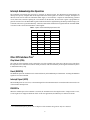
Hardware Description
The TNT4882 has two different pin configurations – ISA and Generic. This application uses the TNT4882 in Generic
pin configuration. Refer to Chapter 5 in the TNT4882 Programmer Reference Manual for a Generic pin description.
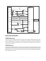
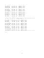
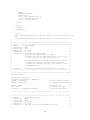
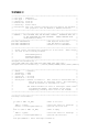
Figure 1 shows the MC68340 and TNT4882 hardware interface diagram. The interface logic can be implemented
easily in a Programmable Array Logic (PAL) device such as a 16V8.
—————————————————
Product and company names are trademarks or trade names of their respective companies.
340993B-01
© Copyright 1997 National Instruments Corporation. All rights reserved.
December 1997
MC68340
TNT4882AQ
5
ADDR4-0
A6-2
16
DATA15-0
D15-0
R/W
RDN
DACKN1
DSN
WRN
DAKN
DREQN1
DRQ
IRQN3
INTR
XTAL1
40 MHz CMOS
OSCILLATOR
RESETN
CSN
ABSUN
RESETN
CSN2
A0
BBUSN
SIZ0
RDY1
DSACKN1
CPUACC PAGED
Figure 1. MC68340 and TNT4882 Interface Hardware Diagram
Synchronous Bus Operation
TNT4882 Address Lines
Address lines A6-A2 of MC68340 connect directly to the address lines of TNT4882. Although TNT4882 only requires
32 bytes of address space a total of 256 bytes are assigned. To take advantage of the longword instructions in
MC68340, TNT4882 FIFOs must be aligned on a word boundary. For this reason the A6-A2 lines of MC68340 are
connected to A4-A0 lines of the TNT4882 chip. Thus every TNT4882 register is assigned to four consecutive address
location for a total of 256 bytes.
TNT4882 Data Lines
Since the TNT4882 has built-in transceivers, the data lines connect directly to the CPU without requiring any external
pull-up resistors. All TNT4882 registers require 8-bit transfers except FIFO B that allows both 8-bit and 16 bit data
transfers. 8-bit I/O accesses can use either data bus. The selection of the data bus is controlled by the ABUSN and
BBUSN signals. The only allowed 16-bit accesses are reads and writes to FIFO B. ABUSN and BBUSN must both be
asserted during 16-bit I/O accesses.
2
TNT4882 ABUSN, BBUSN Signals
The TNT4882 has the capability of using either of its data busses for 8-bit I/O accesses. Either Bus A (D15-8) or Bus
B (D7-0) can be selected using the ABUSN and BBUSN signals. These two signals can be controlled by using SIZ0
and A0 signals of the processor. Whenever accesses are made to an odd byte address, the processor uses the lower byte
of the data bus and whenever accesses are made to an even byte address, the processor uses the upper byte of the data
bus. Table 1 shows the ABUSN and BBUSN signals with respect to SIZ0 and A0.
Table 1. ABUSN and BBUSN Signal of TNT4882
MC68340
TNT4882
Transfer Case
SIZ0
A0
ABUSN
BBUSN
Type of Access
Word Access OR Longword
Access
0
0
0
0
16-bit Access
Not Used
0
1
X
X
NONE
Even Byte Access
1
0
0
1
8-bit Access on Upper Byte
Lane
Odd Byte Access
1
1
1
0
8-bit Access on Lower Byte
Lane
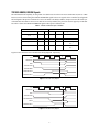
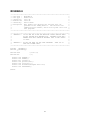
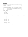
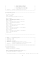
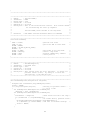
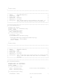
Figures 2 and 3 show the CPU read and write timing diagrams, respectively.
CLK
S0
S1
S2
S3
S4
S5
S0
S5
S0
ADDR R/W
DSN
TNT4882 CSN
TNT4882 RDN
TNT4882 DATA
TNT4882 RDY1
Figure 2. CPU Read Timing Diagram
CLK
S0
S1
S2
S3
S4
ADDR R/W
DSN
TNT4882 CSN
TNT4882 WRN
DATA
TNT4882 RDY1
Figure 3. CPU Write Timing Diagram
3
TNT4882 RDN, WRN Signals
During write accesses, the TNT4882 latches data on the rising edge of WRN. The TNT4882 drives its data buses when
RDN is asserted during read accesses. The processor asserts DSN to indicate that an external device should place valid
data on the bus during a read access, and that valid data is on the data bus during a write access. The R/W signal
indicates the direction of data transfer on the bus. When Direct Memory Access (DMA) is used, DACKN is asserted
by the CPU to indicate that a word is being transferred. Since we are implementing single address DMA, DACKN and
R/W signals should be used to control RDN and WRN during DMA accesses. Table 2 shows the RDN and WRN
signals with respect to R/W, DSN, DACKN.
Table 2. RDN and WRN Signals of TNT4882
MC68340
TNT4882
R/W
DSN
DACKN
RDN
WRN
0
0
0
0
1
0
0
1
1
0
0
1
0
0
1
0
1
1
1
1
1
0
0
1
0
1
0
1
0
1
1
1
0
1
0
1
1
1
1
1
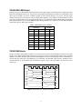
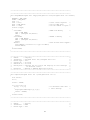
TNT4882 DMA Signals
The processor has a built-in DMA controller so our system does not require an external DMA controller. The system
supports 16-bit Single Address DMA transfers between system memory and the TNT4882 FIFOs. Only one DMA
channel is used. Since MC68340 will start DMA when DREQN1 is asserted, the DRQ signal of the TNT4882 must be
inverted and then connected to the DREQN1 pin of MC68340. The DACKN signal from the TNT4882 can be
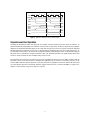
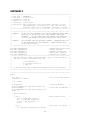
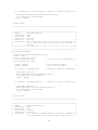
connected directly to the DACKN1 pin of MC68340. Figures 4 and 5 show the DMA read and write cycles
respectively.
DMA Cycle
CPU Cycle
CLK
S0
S1
S2
S3
S4
S5
S0
S1
S2
S3
S4
S5
ADDR
ASN
DSN
R/W
DATA
DRQ
(TNT)
DACKN
WRN
RDY1
Figure 4. DMA Read (Memory to TNT4882) Timing Diagram
4
S0
CPU Cycle
CLK
S0
S1
S2
S3
DMA Cycle
S4
S5
S0
S1
S2
S3
S4
S5
S0
ADDR
ASN
DSN
R/W
DATA
DRQ
(TNT)
DACKN
RDN
Figure 5. DMA Write (TNT4882 to Memory) Timing Diagram
Asynchronous Bus Operation
Normally, the TNT4882 is used in one chip mode. See Chapter 2 in the TNT4882 Programmer Reference Manual. To
maintain backwards compatibility, the TNT4882 can be used in two chip mode. In the two chip mode, the TNT4882
duplicates the Turbo488/NAT4882 chipset. In two chip mode the processor can access registers in both the Turbo488
and NAT4882 but all NAT4882 accesses have to pass through the Turbo488, hence they take a little longer time. To
accommodate for this feature, one can use the asynchronous timing of MC68340 processor. Asynchronous timing on
MC68340 can be controlled by using the DSACKNx pins. The TNT4882 provides two signals namely RDY1 and
CPUACC which can allow the user to handle delays in I/O accesses.
The TNT4882 asserts CPUACC to indicate the processor to lengthen the current I/O access. RDY1 indicates that the
TNT4882 is ready for the host interface to complete the lengthened cycle if CPUACC is asserted. If CPUACC is not
asserted, RDY1 indicates that the current I/O cycle does not need to be lengthened, it does not indicate that the current
cycle has finished. Therefore, DSACKN1 should be negated when CPUACC is asserted and RDY1 is negated. See
Chapter 5 in the TNT4882 Programmer Reference Manual.
5
Interrupt Acknowledge Bus Operation
The TNT4882 can interrupt the processor by asserting its interrupt signal. The MC68340 will acknowledge the
interrupt if its priority is higher than the interrupt mask in the status register. For the above example, interrupt level
three has been selected. Since the TNT4882 cannot supply a vector number, it requests an automatically generated
vector (autovector). Instead of placing the vector number on the data bus, the autovector register is programmed to
generate an autovector. The DSACKNx signals of MC68340 must be negated during the interrupt acknowledge cycle
so that the autovector is generated internally. Therefore, DSACKN1 should also be negated when the TNT4882 INTR
is asserted. Table 3 shows the DSACKN1 control signals:
Table 3. Signals Used for Controlling Asynchronous I/O
TNT4882
MC68340
RDY1
CPUACC
INTR
DSACKN1
0
0
0
0
0
0
1
1
0
1
0
1
0
1
1
1
1
0
0
0
1
0
1
1
1
1
0
0
1
1
1
1
Other CPU Interface Pins1
Chip Select (CSN)
The CSN pin of the TNT4882 can be connected to one of the available chip select pins of the processor. This allows
the chip select to be controlled in software which provides us with some flexibility in moving the TNT4882 anywhere
in MC68340 memory map.
Reset (RESETN)
The RESETN pin of the TNT4882 can be connected directly to the RESETN pin of MC68340. Asserting the RESETN
signal will reset the TNT4882.
Interrupt Signal (INTR)
MC68340 IRQ lines are active low, so the INTR signal from the TNT4882 must be inverted and then connected to one
of the available interrupt lines.
PAGED Pin
When the PAGED pin on the TNT4882 is asserted, the TNT4882 enters the Paged-In state. If Page-In state is true,
several registers are mapped to different offsets. In all new applications, PAGED may be connected to GND.
1
For a detailed description, please refer to Chapter 5 of the TNT4882 Programmer Reference Manual.
6
MODE Pin
The MODE pin determines whether the TNT4882 enters Turbo+7210 mode or Turbo+9914 mode after a hardware
reset. For the above interface, MODE was left unconnected so that the TNT4882 enters the Turbo+7210 mode. See
the MODE & SWAPN Pin Recommendations section of the TNT4882 Programmer Reference Manual.
SWAPN Pin
The TNT4882 samples the SWAPN pin during a hardware reset. If SWAPN is asserted during a hardware reset, the
SWAP bit is set. For the above interface, SWAPN pin was left unconnected. See the MODE & SWAPN Pin
Recommendations section of the TNT4882 Programmer Reference Manual.
FIFO_RDY Pin
The FIFO_RDY output indicates that the FIFOs are ready for at least 8 word (or byte) transfers. Since we did not have
any use for FIFO_RDY, it was left unconnected.
ABUS_OEN and BBUS_OEN
The ABUS_OEN output asserts when the TNT4882 drives Data Bus A during a read access. The BBUS_OEN output
asserts when the TNT4882 drives Data Bus B during a read access. Since we did not have any use for the above pins,
they were left unconnected.
BURST_RDN
When BURST_RDN is asserted, the TNT4882C drives Data Bus A and Data Bus B with the next word to be read from
the FIFOs. BURST_RDN does not remove data from the FIFOs. For the above interface, BURST_RDN was left
unconnected.
Key Pins (KEYRSTN, KEYDQ, KEYCLKN)
The key pins are designed to be connected to a Dallas Semiconductor DS1204U Electronic Key. Applications that do
not use the key can leave the key pins unconnected.
GPIB Device Status Pins
The TNT4882 has five device status pins: TADCS, LADCS, TRIG, DCAS, and REM. All device status pins are output
only so we left them unconnected. For further description of the status pins, refer to the TNT4882 Programmer
Reference Manual.
GPIB Signal Pins
Connect the GPIB signal pins directly to a GPIB connector.
Oscillator Pins (XTALI, XTALO)
A 40-MHz oscillator is required to drive the clock signal. Connect the oscillator output to the XTALI pin of the
TNT4882; leave the XTALO pin unconnected.
Vcc and GND Pins
Supply power to all the Vcc pins and connect the ground signal to all the GND pins.
7
Software Consideration
Once the hardware interface has been constructed, a few initialization routines need to be performed. Once these
initialization sequences are complete, the CPU can be programmed to implement any GPIB device.
System Configuration
System configuration must be performed before the TNT4882 can be used. Configuration of the system requires you
to initialize and configure the System Integration Module (SIM), the interrupt registers, and the DMA channel. Once
you have configured these modules, the MC68340-TNT4882 interface is fully functional.
System Integration Module Configuration
Configure the appropriate chip select registers in the SIM so that the TNT4882 can be selected. With the above setup,
256 bytes are required. Therefore, CSN2 registers are configured and the TNT4882 is located at $00FFE800 in
MC68340 address space. Table 4 shows the register map of the TNT4882 in MC68340 address space. As you can see,
every register in the TNT4882 can be accessed by four different addresses. This setup allows you to use longword
accesses from the FIFOs and gives you the choice of using either the upper byte lane or the lower byte lane.
Table 4. Register Map of the TNT4882 in MC68340 Address Space
REGISTER
ADDRESS SPACE
DIR/CDOR
$FFE800 - $FFE803
ISR1/IMR1
$FFE808 - $FFE80B
ISR2/IMR2
$FFE810 - $FFE813
ACCWR
$FFE814 - $FFE817
SPSR/SPMR
$FFE818 - $FFE81B
INTR
$FFE81C - $FFE81F
ADSR/ADMR
$FFE820 - $FFE823
CNT2
$FFE824 - $FFE827
CPTR/AUXMR
$FFE828 - $FFE82B
CNT3
$FFE82C - $FFE82F
ADR0/ADR
$FFE830 - $FFE833
HSSEL
$FFE834 - $FFE837
ADR1/EOSR
$FFE838 - $FFE83B
STS1/CFG
$FFE840 - $FFE843
DSR/SH_CNT
$FFE844 - $FFE847
IMR3
$FFE848 - $FFE84B
HIER
$FFE84C - $FFE84F
CNT0
$FFE850 - $FFE853
MISC
$FFE854 - $FFE857
CNT1
$FFE858 - $FFE85B
CSR/KEYREG
$FFE85C - $FFE85F
FIFO B
$FFE860 - $FFE863
FIFO A
$FFE864 - $FFE867
ISR3/CCR
$FFE868 - $FFE86B
SASR/DCR
$FFE86C - $FFE86F
STS2/CMDR
$FFE870 - $FFE873
ISR0/IMR0
$FFE874 - $FFE877
TIMER
$FFE878 - $FFE87B
BSR/BCR
$FFE87C - $FFE87F
8
Interrupt Configuration
Since the above setup requires an autovector, we need to program the autovector register so that the vector number is
generated internally when an interrupt is acknowledged. In the above case, we are using interrupt level three, therefore
$08 should be stored in the autovector register.
The vector table should also be modified to point to the new interrupt handler. For interrupt level three, the vector is
stored at location $06C. The value contained at this memory location should be modified to contain the address of the
new interrupt handler.
DMA Channel Configuration
In order to use DMA, the DMA channel must be configured for single address, burst mode, and external request
generation. On GPIB reads, the TNT4882 will assert its DRQ signal if the FIFOs contain a byte that needs to be
transferred to memory. On GPIB writes, the TNT4882 will assert its DRQ signal when the FIFOs are not full.
For every system there is a point where programmed I/O is faster than DMA I/O and vice versa. Programmed I/O is
usually faster for small transfer sizes (500 bytes or less). It is recommended that you determine the crossover point and
then use it as a switch to decide when to use programmed I/O or DMA.
Device Level Programs
We recommend using the TNT4882 in one-chip mode. The TNT4882 by default powers up in two-chip mode to
maintain backwards compatibility. Therefore, it is important to initialize the TNT4882 so that it is in one-chip mode.
Follow the steps listed in the GPIB ESP-488TL Software Reference Manual for TNT4882. The manual also includes
sample routines that can help you write programs for the TNT4882.
Hardware Interface Test
A hardware interface test and library is included with this package. Before you use the hardware test, make any
changes if necessary to the header files and re-compile the program. We used Microtec Research Software
Development Tools, version 4.2D for DOS and an M68340EVS System. The header files include information such as
the base address where the TNT4882 is located. The hardware interface test program tests the interface between
MC68340 and TNT4882. It performs three different types of I/O:
•
Programmed I/O
•
Interrupt Driven I/O
•
DMA I/O
To perform the hardware test, download the HARDWARE.ABS file on the MC68340EVS system. The HARDWARE.ABS file is in the HARDWARE directory.
9
Downloading Procedures
A Widows terminal settings file is also included on the disk. Execute the following steps to download a program:
1.
Start Windows.
2.
Choose RUN from the FILE menu.
3.
Type A:\MC68340.TRM to start the Windows Terminal program.
4.
Type LO and press <ENTER>.
5.
Choose Send Text File from the Transfers menu.
6.
Select HARDWARE.ABS from A:\HARDWARE directory.
7.
When download has completed, hit <ENTER> twice.
Once the program has been downloaded, use the RM command to initialize the MC68340 registers. Set PC to $4000,
USP to $8000 and SSP to $10000.
Programmed I/O Test
In Programmed I/O, 5 different tests are conducted that make accesses to FIFOs. These five tests are:
1.
8 Bit Accesses to FIFO A
2.
8 Bit Accesses to FIFO B
3.
16 Bit Accesses to FIFOs
4.
8 Bit Writes and 16 Bit Reads
5.
16 Bit Writes and 8 Bit Reads
Programmed I/O tests 1 and 2 write all possible values (0-255) to both the FIFOs using the upper byte lane and the
lower byte lane. Test 3 makes 16-bit accesses to the FIFOs by writing specific values which test the address and data
lines (stuck-0,stuck-1,stuck-together). Tests 4 and 5 write the exact same values as in test 3, but 8 bit write and 16 bit
read is performed in test 4 while the opposite is performed in test 5. These tests make sure that the FIFOs can be
accessed properly and also test the hardware interface such as the address lines, data lines and bus operation signals.
Interrupt Driven I/O Test
By performing the Interrupt Driven I/O we are testing to make sure that the TNT4882 can assert its interrupt line and
that it gets acknowledged properly. Before we do any I/O we do a sanity check to make sure that the interrupt handler
has been loaded properly. The program reads the contents of memory location $06C (IRQN3) and compares it with
the address of the interrupt handler. If a mismatch occurs, the interrupt handler is not getting loaded properly, or the
vector table is being altered which results in the loss of the handler address. Once the handler has been loaded properly,
NFF bit of IMR3 is enabled. If FIFOs have room for a byte, an interrupt will occur. After writing to the FIFOs we
enable the NEF bit of IMR3. An interrupt will occur if FIFOs contain bytes that need to be transferred to memory.
If the interrupts do not get acknowledged, chances are that the interrupt line is not connected properly. If an unexpected
interrupt occurs, then your system may have deleted the address of the new handler from the exception vector table.
DMA I/O Test
DMA I/O tests the functionality of the DMA Channel and its associated interface logic. For example, when a DMA
read is performed, data is transferred from memory (read from memory) to the TNT4882. If data transfers do not take
place, chances are that WRN signal is not asserting during the DMA read cycle. Similarly, during a DMA write cycle,
RDN should be asserted because data is transferred from FIFOs to memory.
10
In the DMA I/O test routine, the channel is initialized by clearing the status register and loading the byte transfer value
in the byte counter register. The channel is then started, and DMA takes place when the DREQN1 pin of MC68340
goes low. DMA read takes place first where values are written to the FIFOs. DMA write takes place later where values
are read back from the FIFOs.
MC340BUG Library
A Library is also included with the software package. The MC340BUG library provides basic I/O functions that use
the M340BUG debug system calls. System calls use Trap #15 for I/O functions. Therefore Trap #15 is not available
for user programs. The library was created using Microtec’s Librarian. This library package is only useful if you are
developing programs using Microtec Research Software Development Tools.
Description of Library Functions
ERASLN()
Purpose
Erase the line at the present cursor position
Parameters
NONE
Return Type
void
Example
ERASLN();
NEWLN()
Purpose
Skip a line
Parameters
NONE
Return Type
void
Example
NEWLN();
getchar()
Purpose
Read a character from the input port
Parameters
NONE
Return Type
char
Example
c = getchar();
putchar()
Purpose
Write a character to the output port
Parameters
character to be written
Return Type
void
Example
putchar('a'); putchar(chr) where chr = 'z';
11
puts()
Purpose
Output a line to the output port
Parameters
string to be written
Return Type
void
Example
puts("hello"); puts(str) where str = "how are you?";
PrintHex()
Purpose
Output a number in hexadecimal form
Parameters
unsigned short int (0 - 65535)
Return Type
void
Example
PrintHex(321); PrintHex(num) where num = 3245;
RET340BUG()
Purpose
Restore control to 340Bug from the target program
Parameters
NONE
Return Type
void
Example
RET340BUG();
References
1.
MC68340 Integrated Processor with DMA User’s Manual, Motorola Inc., 1992.
2.
TNT4882 Programmer Reference Manual, National Instruments, 1994.
3.
ESP-488TL Software Reference Manual for TNT4882, National Instruments, 1994.
4.
M68340BUG Debug Monitor and Assembler User’s Manual, Motorola Inc., 1991.
5.
M68340EVS Evaluation System User’s Manual, Motorola Inc., 1991.
Appendix
Source File
Description
Page
Register.H
TNT4882 Register Declarations
12
MC68340.H
MC68340 Register Declarations
17
MC340BUG.H
340 Bug Debug Monitor Functions
19
HARDWARE.H
Test Program Header File
19
HARDWARE.C
Test Program Source Code
20
TNT4882.H
TNT4882 Test Function Declarations
26
TNT4882.C
TNT4882 Test Functions
26
12
Register.H
#ifndef __REGISTER_H
#define __REGISTER_H
#define BASE
0x00FFE800
#define DIR
*(unsigned char *) (BASE + 0x00)
#define CDOR
*(unsigned char *) (BASE + 0x00)
#define IMR0
*(unsigned char *) (BASE + 0x75)
#define E_BTO
0x10
#define E_GLINT
0x80
#define ISR0
*(unsigned char *) (BASE + 0x75)
#define E_SYNC
0x01
#define E_TO
0x02
#define E_ATNI
0x04
#define E_IFCI
0x08
#define E_EOS
0x10
#define E_NL
0x20
#define E_STBO
0x40
#define E_CDBA
0x80
#define IMR1
*(unsigned char *) (BASE + 0x08)
#define ISR1
*(unsigned char *) (BASE + 0x08)
#define E_DI
0x01
#define E_DO
0x02
#define E_ERR
0x04
#define E_DEC
0x08
#define E_END
0x10
#define E_DET
0x20
#define E_APT
0x40
#define E_isrCPT 0x80
#define IMR2
*(unsigned char *) (BASE + 0x10)
#define E_DMAI
0x10
#define E_DMAO
0x20
#define ISR2
*(unsigned char *) (BASE + 0x10)
#define E_ADSC
0x01
#define E_REMC
0x02
#define E_LOKC
0x04
#define E_REM
0x10
#define E_LOK
0x20
#define E_INT
0x80
#define IMR3
*(unsigned char *) (BASE + 0x48)
#define E_DONE
0x01
#define E_TLCINT 0x02
#define E_NEF
0x04
#define E_NFF
0x08
#define E_STOP
0x10
#define E_SRQ
0x20
#define E_INTSR
0x40
#define ISR3
*(unsigned char *) (BASE + 0x68)
#define E_X
0x80
#define ACCWR
*(unsigned char *) (BASE + 0x15)
#define SPSR
*(unsigned char *) (BASE + 0x18)
#define B_S1
(SPSR & 0x01)
#define B_S2
(SPSR & 0x02)
13
#define
#define
#define
#define
#define
#define
B_S3
B_S4
B_S5
B_S6
B_PEND
B_S8
(SPSR
(SPSR
(SPSR
(SPSR
(SPSR
(SPSR
&
&
&
&
&
&
0x04)
0x08)
0x10)
0x20)
0x40)
0x80)
#define SPMR
*(unsigned char *) (BASE + 0x18)
#define E_S1
0x01
#define E_S2
0x02
#define E_S3
0x04
#define E_S4
0x08
#define E_S5
0x10
#define E_S6
0x20
#define E_PEND
0x40
#define E_S8
0x80
#define INTR
*(unsigned char *) (BASE + 0x1D)
#define ADSR
*(unsigned
#define B_MJMN
(ADSR
#define B_TA
(ADSR
#define B_LA
(ADSR
#define B_TPAS
(ADSR
#define B_LPAS
(ADSR
#define B_SPMS
(ADSR
#define B_ATN1
(ADSR
#define B_CIC
(ADSR
char *) (BASE + 0x20)
& 0x01)
& 0x02)
& 0x04)
& 0x08)
& 0x10)
& 0x20)
& 0x40)
& 0x80)
#define ADMR
*(unsigned char *) (BASE + 0x20)
#define NoAddr
0x30
#define NormDual 0x31
#define ExSingle 0x32
#define ExDual
0x33
#define ListOnly 0x70
#define TalkOnly 0xB0
#define CPTR
*(unsigned char *) (BASE + 0x28)
#define AUXMR
*(unsigned char *) (BASE + 0x28)
#define
#define
#define
#define
#define
#define
#define
#define
#define
#define
#define
#define
#define
#define
#define
#define
#define
#define
#define
#define
#define
#define
#define
PON
ClrIST
RstChip
RHDF
TRIG
ClrRTL
SEOI
NonValid
RQC
SetIST
RLC
LUT
LUL
SetRTL
NBAF
Valid
GTS
TCA
TCS
LTN
DisRSC
Turbo9914
ClrIFC
0x00
0x01
0x02
0x03
0x04
0x05
0x06
0x07
0x08
0x09
0x0A
0x0B
0x0C
0x0D
0x0E
0x0F
0x10
0x11
0x12
0x13
0x14
0x15
0x16
14
#define
#define
#define
#define
#define
#define
#define
#define
#define
#define
#define
#define
#define
#define
#define
#define
#define
#define
#define
#define
#define
#define
#define
ClrREN
REQT
REQF
TCSE
LTNnCont
LUN
RPPL
SetIFC
SetREN
PageIn
HLDI
ClrDET
ClrEND
ClrDEC
ClrERR
ClrSRQI
ClrLOKC
ClrREMC
ClrADSC
ClrIFCI
ClrATNI
ClrSYNC
SetSYNC
0x17
0x18
0x19
0x1A
0x1B
0x1C
0x1D
0x1E
0x1F
0x50
0x51
0x54
0x55
0x56
0x57
0x58
0x59
0x5A
0x5B
0x5C
0x5D
0x5E
0x5F
#define PPR
0x60
#define P(value)
(PPR | value)
#define E_S
(PPR | 0x08)
#define E_U
(PPR | 0x10)
#define AUXRA
#define E_HLDA
#define E_HLDE
#define E_REOS
#define E_XEOS
#define E_BIN
0x80
(AUXRA
(AUXRA
(AUXRA
(AUXRA
(AUXRA
|
|
|
|
|
0x01)
0x02)
0x04)
0x08)
0x10)
#define AUXRB
0xA0
#define E_auxCPT
(AUXRB
#define E_SPEOI
(AUXRB
#define E_TRI
(AUXRB
#define E_ISS
(AUXRB
|
|
|
|
0x01)
0x02)
0x04)
0x80)
#define AUXRE
#define E_DHDC
#define E_DHDT
#define E_DHADC
#define E_DHADT
0xC0
(AUXRE
(AUXRE
(AUXRE
(AUXRE
|
|
|
|
0x01)
0x02)
0x04)
0x08)
#define AUXRF
0xD0
#define E_DHALL
(AUXRF
#define E_DHUNTL
(AUXRF
#define E_DHALA
(AUXRF
#define E_DHATA
(AUXRF
|
|
|
|
0x01)
0x02)
0x04)
0x08)
|
|
|
|
0x01)
0x02)
0x04)
0x08)
#define AUXRG
0x40
#define E_CHES
(AUXRG
#define E_DISTCT
(AUXRG
#define E_RPP2
(AUXRG
#define E_NTNL
(AUXRG
#define AUXRI
0xE0
#define E_SISB
(AUXRI
#define E_PP2
(AUXRI
#define E_USTD
(AUXRI
| 0x01)
| 0x04)
| 0x08)
15
#define AUXRJ
0xF0
#define TM(value) (AUXRJ | value)
#define
#define
#define
#define
CNT3
CNT2
CNT1
CNT0
*(unsigned
*(unsigned
*(unsigned
*(unsigned
#define ADR0
*(unsigned
#define F_ADR0
(ADR0
#define B_DL0
(ADR0
#define B_DT0
(ADR0
char
char
char
char
*)
*)
*)
*)
(BASE
(BASE
(BASE
(BASE
+
+
+
+
0x2D)
0x25)
0x58)
0x50)
char *) (BASE + 0x30)
& 0x1F)
& 0x20)
& 0x40)
#define ADR
*(unsigned char *) (BASE + 0x30)
#define ADDR(val) (ADR | val)
#define E_DL
0x20
#define E_DT
0x40
#define E_ARS
0x80
#define HSSEL
*(unsigned char *) (BASE + 0x35)
#define E_ONEC
0x01
#define E_NODMA
0x10
#define E_GO2SIDS 0x20
#define ADR1
*(unsigned
#define F_ADR1
(ADR1
#define B_DL1
(ADR1
#define B_DT1
(ADR1
#define B_EOI1
(ADR1
#define EOSR
char *) (BASE + 0x38)
& 0x1F)
& 0x20)
& 0x40)
& 0x80)
*(unsigned char *) (BASE + 0x38)
#define STS1
*(unsigned
#define B_GSYNC
(STS1
#define B_HALT
(STS1
#define B_DAV
(STS1
#define B_stsSTOP (STS1
#define B_DRQ
(STS1
#define B_IN
(STS1
#define B_SC
(STS1
#define B_stsDONE (STS1
char *) (BASE + 0x40)
& 0x01)
& 0x02)
& 0x04)
& 0x08)
& 0x10)
& 0x20)
& 0x40)
& 0x80)
#define CFG
*(unsigned char *) (BASE + 0x40)
#define E_168N
0x01
#define E_TIM
0x02
#define E_TMOE
0x04
#define E_CCEN
0x08
#define E_ABN
0x10
#define E_IN
0x20
#define E_TLCHLTE 0x40
#define E_COMMAND 0x80
#define DSR
*(unsigned char *) (BASE + 0x45)
#define SHCNT
*(unsigned char *) (BASE + 0x45)
#define pt1
0x00
#define E_PT1
(pt1 | 0x20)
#define PT1(value) (pt1 | value)
#define t17
0x40
#define T17(value) (t17 | value)
#define t12
0x80
#define T12(value) (t12 | value)
16
#define t13
0xC0
#define T13(value) (t13 | value)
#define HIER
*(unsigned char *) (BASE + 0x4D)
#define E_PMTwEOS 0x01
#define E_NTSETUP 0x10
#define E_DGB
0x40
#define E_DGA
0x80
#define MISC
*(unsigned char *) (BASE + 0x55)
#define E_NOTS
0x01
#define E_NOAS
0x02
#define E_WRAP
0x04
#define E_SLOW
0x08
#define E_HSE
0x10
#define CSR
*(unsigned char *) (BASE + 0x5D)
#define KEYREG
*(unsigned char *) (BASE + 0x5D)
#define FIFO
*(unsigned short int *) (BASE + 0x60)
#define FIFOB
*(unsigned char *) (BASE + 0x60)
#define FIFOA
*(unsigned char *) (BASE + 0x65)
#define CCR
*(unsigned char *) (BASE + 0x68)
#define SASR
*(unsigned
#define B_SH1B
(SASR
#define B_SH1A
(SASR
#define B_ACRDY
(SASR
#define B_ADHS
(SASR
#define B_ANHS2
(SASR
#define B_ANHS1
(SASR
#define B_AEHS
(SASR
#define B_NBA1
(SASR
#define DCR
char *) (BASE + 0x6D)
& 0x01)
& 0x02)
& 0x04)
& 0x08)
& 0x10)
& 0x20)
& 0x40)
& 0x80)
*(unsigned char *) (BASE + 0x6D)
#define STS2
*(unsigned
#define B_BEFN
(STS2
#define B_BFFN
(STS2
#define B_AEFN
(STS2
#define B_AFFN
(STS2
#define B_168N
(STS2
char *) (BASE + 0x70)
& 0x01)
& 0x02)
& 0x04)
& 0x08)
& 0x40)
#define CMDR
*(unsigned char *) (BASE + 0x70)
#define DiSysCon 0x02
#define EnSysCon 0x03
#define GO
0x04
#define STOP
0x08
#define RstFIFO
0x10
#define SftRst
0x22
#define TIMER
*(unsigned char *) (BASE + 0x78)
#define BSR
*(unsigned char *) (BASE + 0x7D)
#define B_REN
(BSR & 0x01)
#define B_IFC
(BSR & 0x02)
#define B_bsrSRQ (BSR & 0x04)
#define B_EOI
(BSR & 0x08)
#define B_NRFD
(BSR & 0x10)
#define B_NDAC
(BSR & 0x20)
17
#define
#define
B_bsrDAV
B_ATN
(BSR & 0x40)
(BSR & 0x80)
#define BCR
*(unsigned char *) (BASE + 0x7D)
#define E_REN
0x01
#define E_IFC
0x02
#define E_bcrSRQ 0x04
#define E_EOI
0x08
#define E_NRFD
0x10
#define E_NDAC
0x20
#define E_bcrDAV 0x40
#define E_ATN
0x80
#endif
18
MC68340.H
#ifndef __MC68340_H
#define __MC68340_H
#define MCBASE
0xFFFFF000
/**********************System Integration Module (SIM)**********************/
#define AVR
*(unsigned char *) (MCBASE + 0x006)
#define RSR
*(unsigned char *) (MCBASE + 0x007)
#define PORTA
*(unsigned char *) (MCBASE + 0x011)
#define DDRA
*(unsigned char *) (MCBASE + 0x013)
#define PPARA1 *(unsigned char *) (MCBASE + 0x015)
#define PPARA2 *(unsigned char *) (MCBASE + 0x017)
#define PORTB
*(unsigned char *) (MCBASE + 0x019)
#define PORTB1 *(unsigned char *) (MCBASE + 0x01B)
#define DDRB
*(unsigned char *) (MCBASE + 0x01D)
#define PPARB
*(unsigned char *) (MCBASE + 0x01F)
#define SWIV
*(unsigned char *) (MCBASE + 0x020)
#define SYPCR
*(unsigned char *) (MCBASE + 0x021)
#define SWSR
*(unsigned char *) (MCBASE + 0x027)
#define SIMMCR *(unsigned short int *) (MCBASE + 0x000)
#define SYNCR
*(unsigned short int *) (MCBASE + 0x004)
#define PICR
*(unsigned short int *) (MCBASE + 0x022)
#define PITR
*(unsigned short int *) (MCBASE + 0x024)
#define CSAMR0 *(unsigned int *) (MCBASE + 0x040)
#define CSBAR0 *(unsigned int *) (MCBASE + 0x044)
#define CSAMR1 *(unsigned int *) (MCBASE + 0x048)
#define CSBAR1 *(unsigned int *) (MCBASE + 0x04C)
#define CSAMR2 *(unsigned int *) (MCBASE + 0x050)
#define CSBAR2 *(unsigned int *) (MCBASE + 0x054)
#define CSAMR3 *(unsigned int *) (MCBASE + 0x058)
#define CSBAR3 *(unsigned int *) (MCBASE + 0x05C)
/***************************************************************************/
/************************Direct Memory Access (DMA)*************************/
#define DMAMCR1 *(unsigned short int *) (MCBASE + 0x780)
#define INTR1
*(unsigned short int *) (MCBASE + 0x784)
#define CCR1
*(unsigned short int *) (MCBASE + 0x788)
#define CSR1
*(unsigned char *) (MCBASE + 0x78A)
#define FCR1
*(unsigned char *) (MCBASE + 0x78B)
#define SAR1
*(unsigned int *) (MCBASE + 0x78C)
#define DAR1
*(unsigned int *) (MCBASE + 0x790)
#define BTC1
*(unsigned int *) (MCBASE + 0x794)
#define DMAMCR2 *(unsigned short int *) (MCBASE + 0x7A0)
#define INTR2
*(unsigned short int *) (MCBASE + 0x7A4)
#define CCR2
*(unsigned short int *) (MCBASE + 0x7A8)
#define CSR2
*(unsigned char *) (MCBASE + 0x7AA)
#define FCR2
*(unsigned char *) (MCBASE + 0x7AB)
#define SAR2
*(unsigned int *) (MCBASE + 0x7AC)
#define DAR2
*(unsigned int *) (MCBASE + 0x7B0)
#define BTC2
*(unsigned int *) (MCBASE + 0x7B4)
/***************************************************************************/
/*****************************Serial Modules********************************/
#define SMCR
*(unsigned short int *) (MCBASE + 0x700)
#define ILR
*(unsgined char *) (MCBASE + 0x704)
#define IVR
*(unsigned char *) (MCBASE + 0x705)
#define MR1A
*(unsigned char *) (MCBASE + 0x710)
#define SRA
*(unsigned char *) (MCBASE + 0x711)
#define CSRA
*(unsigned char *) (MCBASE + 0x711)
#define CRA
*(unsigned char *) (MCBASE + 0x712)
#define RBA
*(unsigned char *) (MCBASE + 0x713)
#define TBA
*(unsigned char *) (MCBASE + 0x713)
19
#define MR2A
*(unsigned char *) (MCBASE + 0x720)
#define MR1B
*(unsigned char *) (MCBASE + 0x718)
#define SRB
*(unsigned char *) (MCBASE + 0x719)
#define CSRB
*(unsigned char *) (MCBASE + 0x719)
#define CRB
*(unsigned char *) (MCBASE + 0x71A)
#define RBB
*(unsigned char *) (MCBASE + 0x71B)
#define TBB
*(unsigned char *) (MCBASE + 0x71B)
#define MR2B
*(unsigned char *) (MCBASE + 0x721)
#define IPCR
*(unsigned char *) (MCBASE + 0x714)
#define ACR
*(unsigned char *) (MCBASE + 0x714)
#define ISR
*(unsigned char *) (MCBASE + 0x715)
#define IER
*(unsigned char *) (MCBASE + 0x715)
#define IP
*(unsigned char *) (MCBASE + 0x71D)
#define OPCR
*(unsigned char *) (MCBASE + 0x71D)
#define OPS
*(unsigned char *) (MCBASE + 0x71E)
#define OPR
*(unsigned char *) (MCBASE + 0x71F)
/***************************************************************************/
/******************************Timer Modules********************************/
#define TMMCR1 *(unsigned short int *) (MCBASE + 0x600)
#define IR1
*(unsigned short int *) (MCBASE + 0x604)
#define CR1
*(unsigned short int *) (MCBASE + 0x606)
#define SR1
*(unsigned short int *) (MCBASE + 0x608)
#define CNTR1
*(unsigned short int *) (MCBASE + 0x60A)
#define PREL1T1 *(unsigned short int *) (MCBASE + 0x60C)
#define PREL2T1 *(unsigned short int *) (MCBASE + 0x60E)
#define COM1
*(unsigned short int *) (MCBASE + 0x610)
#define TMMCR2 *(unsigned short int *) (MCBASE + 0x640)
#define IR2
*(unsigned short int *) (MCBASE + 0x644)
#define CR2
*(unsigned short int *) (MCBASE + 0x646)
#define SR2
*(unsigned short int *) (MCBASE + 0x648)
#define CNTR2
*(unsigned short int *) (MCBASE + 0x64A)
#define PREL1T2 *(unsigned short int *) (MCBASE + 0x64C)
#define PREL2T2 *(unsigned short int *) (MCBASE + 0x64E)
#define COM2
*(unsigned short int *) (MCBASE + 0x650)
/***************************************************************************/
#endif
20
MC340BUG.H
/*************************************************************************/
/* File Name : MC340BUG.H
*/
/* File Type : Header File
*/
/* Created On : 03/17/95
*/
/* Modified On: 06/05/95
*/
/* Created By : Faisal Habib
*/
/* Description: This header file declares the fuctions that are
*/
/*
provided in the 340Bug Monitor. The functions use
*/
/*
340Bug Trap #15 handler, which allow system calls from */
/*
user programs.
*/
/*************************************************************************/
/*************************************************************************/
/* WARNING!! : IF YOU ARE NOT USING THE MOTOROLA 340BUG MONITOR THEN
*/
/*
DO NOT INCLUDE THIS HEADER FILE. PROGRAMS USING THIS
*/
/*
HEADER FILE WILL FUNCTION PROPERLY ONLY IF THE 340BUG
*/
/*
IS USED.
*/
/*
*/
/* WARNING!! : DO NOT USE TRAP #15 FOR USER PROGRAMS. TRAP #15 IS
*/
/*
USED FOR SYSTEM CALLS.
*/
/*************************************************************************/
#ifndef __MC340BUG_H
#define __MC340BUG_H
#define NULL
#define EOF
extern
extern
extern
extern
extern
extern
extern
void
void
char
void
void
void
void
((void *)0)
(-1)
ERASLN();
NEWLN();
getchar();
putchar(char);
puts(char *);
PrintHex(unsigned short int);
RET340BUG();
#endif
21
HARDWARE.H
/**************************************************************************/
/* File Name : HARDWARE.H
*/
/* File Type : C header file
*/
/* Created On : 05/04/95
*/
/* Modified On: 05/23/95
*/
/* Created By : Faisal Habib
*/
/* Description: This header file contains macros and function prototypes */
/*
for the source program. The source program will test the */
/*
hardware interface for the TNT and MC68340. In particular*/
/*
it will test the three different types of I/O: Programmed,*/
/*
Interrupts, and DMA.
*/
/**************************************************************************/
#ifndef __HARDWARE_H
#define __HARDWARE_H
#define
#define
#define
#define
WRITE
READ
IARB
IRQ3
0
1
0x0008
0x08
#define AVECIRQ3 0x0000006C
#define EnableMC68340Interrupts
#define
#define
#define
#define
#define
DMA_READ
DMA_WRITE
DMA_CONF
DMA_INTR
DMA_SPACE
0x1AA2
0x06A2
0x177A
0x000F
0xDD
#define
#define
#define
#define
#define
DMA_DONE
DMA_BES
DMA_BED
DMA_CON
StartDMA
0x40
0x20
0x10
0x08
CCR1 |= 0x01
asm("
ori.w #$0200,SR","
void ConfigureMC();
char Programmed_IO_Test();
char Interrupt_IO_Test();
char DMA_IO_Test();
char SetupDMA(unsigned char,unsigned int,unsigned short int*);
unsigned short int Check_DMA_Status(unsigned char);
char Compare(unsigned short int*,unsigned short int*);
char Select();
#endif
22
andi.w #$FAFF,SR")
HARDWARE.C
/**************************************************************************/
/* File Name : HARDWARE.C
*/
/* File Type : C source file
*/
/* Created On : 05/04/95
*/
/* Modified On: 05/24/95
*/
/* Created By : Faisal Habib
*/
/* Description: This program will test the hardware interface for the
*/
/*
TNT and MC68340. In particular it will test the three
*/
/*
different types of I/O: Programmed, Interrupts, and DMA. */
/**************************************************************************/
/**************************************************************************/
/* WARNING : DO NOT USE THIS PROGRAM IF YOU USE AN INTERRUPT LEVEL OTHER */
/*
THAN IRQ3 OF THE MC68340 AND A BASE ADDRESS OTHER THAN
*/
/*
$FFFFE800. YOU CAN CHANGE THE BASE ADDRESS AND INTERRUPT
*/
/*
LEVEL IN THE HEADER FILE AND RE-COMPILE THE SOURCE CODE.
*/
/*
*/
/* WARNING : THIS PROGRAM USES THE MC340BUG LIBRARY. THEREFORE TRAP #15 */
/*
IS NOT AVAILABLE FOR USER PROGRAMS. PLEASE REFRAIN FROM
*/
/*
USING TRAP #15 CALLS.
*/
/**************************************************************************/
#include "REGISTER.H"
/*TNT Register Definitions*/
#include "MC340BUG.H"
/*340bug routines
*/
#include "MC68340.H"
/*MC68340 register def.
*/
#include "TEST4882.H"
/*TNT config. functions
*/
#include "HARDWARE.H"
/*Hardware test header
*/
/**************************************************************************/
/* The main routine conducts three different types of tests and prints
*/
/* the final results. The three tests are:
*/
/*
*/
/*
1. Programmed I/O
*/
/*
2. Interrupt Driven I/O
*/
/*
3. DMA I/O
*/
/*
*/
/* To run the above tests, MC68340 and TNT4882 need to be configured.
*/
/**************************************************************************/
/**************************************************************************/
main()
{
char fail;
/*var. for storing results*/
unsigned int counter;
fail = FALSE;
ConfigureMC();
puts("\nMC68340 has been initialized.\n");
InitializeTNT();
puts("\nTNT4882 has been initialized.\n\n");
while (1)
{
switch (Select())
{
case 0:
fail |= Programmed_IO_Test();
fail |= Interrupt_IO_Test();
/*fail |= DMA_IO_Test();*/
break;
case 1:
for (counter=0;counter<500;++counter)
23
/*configure MC68340
*/
/*initialize the TNT4882
*/
/*Test Interface once
*/
/*Loop Test (500 times)
*/
{
NEWLN();
PrintHex(counter);
puts("Loop");
fail |= Programmed_IO_Test();
fail |= Interrupt_IO_Test();
/*fail |= DMA_IO_Test();*/
}
break;
default:
NEWLN();
RET340BUG();
}
if (fail)
puts("\nHardware Diagnostics Completed. Board is not fully functional.\n");
else
puts("\nHardware Diagnostics Completed. Board is fully functional.\n");
}
}
/**************************************************************************/
/**************************************************************************/
/* Module
: ConfigureMC()
*/
/* Parameters : NONE
*/
/* Return Type : void
*/
/* Created On : 05/04/95
*/
/* Modified On : 05/15/95
*/
/* Description : Configures the MC68340 CPU.
*/
/*
Loads the interrupt handler for IRQ3
*/
/*
Configures the SIM for unrestricted data space,no show */
/*
cycles, partial interrupt request mode.
*/
/*
*/
/*
To place the TNT in a different address space, assign
*/
/*
appropriate values to the chip select registers.
*/
/*
To change the interrupt priority, make changes to the
*/
/*
HARDWARE.H file.
*/
/*
*/
/* Reference
: MC68340 User's Manual (MC68340UM/AD Rev 1) Section 4.
*/
/**************************************************************************/
/**************************************************************************/
void ConfigureMC()
{
unsigned int *Exception;
(unsigned int)Exception = AVECIRQ3;
CSBAR2 = 0x00FFEFF1;
/*CS base address register*/
CSAMR2 = 0x000007F3;
/*CS address mask register*/
SIMMCR = IARB;
AVR = IRQ3;
*Exception = (unsigned int)handler;
/*configure SIM
/*autovector for IRQ3
/*load interrupt handler
*/
*/
*/
}
/**************************************************************************/
/**************************************************************************/
/* Module
: Programmed_IO_Test()
*/
/* Parameters : NONE
*/
/* Return Type : char
*/
/* Created On : 05/04/95
*/
/* Modified On : 05/15/95
*/
/* Description : Performs 5 types of Programmed I/O tests:
*/
/*
*/
24
/*
1. 8 Bit accesses to FIFO A
*/
/*
2. 8 Bit accesses to FIFO B
*/
/*
3. 16 Bit accesses to FIFOs
*/
/*
4. 8 Bit WRITES and 16 Bit READS
*/
/*
5. 16 Bit WRITES and 8 Bit READS
*/
/*
*/
/* Reference
: MC68340 & TNT4882 Application Notes
*/
/**************************************************************************/
/**************************************************************************/
char Programmed_IO_Test()
{
char result = FALSE;
HSSEL |= E_NODMA;
puts("\nPerforming Programmed I/O Test.\n");
CMDR =
puts("
result
CMDR =
puts("
result
RstFIFO;
Performing 8 Bit accesses to FIFO A");
|= Test8BitRegister(&FIFOA);
RstFIFO;
Performing 8 Bit accesses to FIFO B");
|= Test8BitRegister(&FIFOB);
CMDR = RstFIFO;
puts("
Performing 16 Bit accesses to FIFOs");
result |= Test16BitRegister();
CMDR = RstFIFO;
puts("
Performing 8 Bit WRITES & 16 Bit READS");
result |= Test8Write16Read();
CMDR = RstFIFO;
puts("
Performing 16 Bit WRITES & 8 BIT READS");
result |= Test16Write8Read();
return result;
}
/**************************************************************************/
/**************************************************************************/
/* Module
: Interrupt_IO_Test()
*/
/* Parameters : NONE
*/
/* Return Type : char
*/
/* Created On : 05/04/95
*/
/* Modified On : 05/15/95
*/
/* Description : Performs Interrupt Driven I/O tests
*/
/*
Checks the installation of the interrupt handler
*/
/* Reference
: MC68340 & TNT4882 Application Notes
*/
/**************************************************************************/
/**************************************************************************/
char Interrupt_IO_Test()
{
unsigned int *Exception;
(unsigned int)Exception = AVECIRQ3;
puts("\nPerforming Interrupt I/O Test.\n");
puts("
Checking Interrupt Handler Installation");
if ((unsigned int)handler != *Exception)
{
puts("Interrupt Handler is not loaded properly. Interrupt Tests will not be per-
25
formed.\n\n");
return ERROR;
}
else
{
Failure = FALSE;
EnableMC68340Interrupts;
IMR3 = E_NFF;
/*write to fifo
*/
while (IMR3 & E_NFF);
EnableMC68340Interrupts;
IMR3 = E_NEF;
/*read from fifo
*/
while (IMR3 & E_NEF);
}
return Failure;
}
/**************************************************************************/
/**************************************************************************/
/* Module
: DMA_IO_Test()
*/
/* Parameters : NONE
*/
/* Return Type : char
*/
/* Created On : 05/04/95
*/
/* Modified On : 05/17/95
*/
/* Description : Performs DMA I/O tests
*/
/* Reference
: MC68340 & TNT4882 Application Notes
*/
/**************************************************************************/
/**************************************************************************/
char DMA_IO_Test()
{
unsigned short int StoreBuf[] =
{'a','b','c','d','e','f','g','h','i','j','k','l','m','n','o','p'};
unsigned short int ReceiveBuf[16];
puts("\nPerforming DMA I/O Test.\n");
HSSEL = E_ONEC;
/*one-chip mode
*/
CMDR = RstFIFO;
/*reset the FIFOs
*/
CFG = 0x11;
/*GPIB Write
puts("
Performing WRITE to FIFOs using DMA");
if (SetupDMA(READ,16,StoreBuf) == ERROR) return ERROR;
StartDMA;
while (BTC1);
*/
CFG = 0x01;
/*GPIB Read
puts("
Performing READ from FIFOs using DMA");
if (SetupDMA(WRITE,16,ReceiveBuf) == ERROR) return ERROR;
StartDMA;
while (BTC1);
*/
return Compare(StoreBuf,ReceiveBuf);
}
/**************************************************************************/
/**************************************************************************/
/* Module
: SetupDMA()
*/
/* Parameters : unsigned char,unsigned int,unsigned short int*
*/
/* Return Type : char
*/
/* Created On : 05/15/95
*/
/* Modified On : 05/17/95
*/
/* Description : Sets and configures the DMA channels for READ or WRITE */
/*
For a different configuration, change the values in the */
/*
HARDWARE.H file.
*/
/*
*/
/* Reference
: MC68340 & TNT4882 Application Notes
*/
26
/**************************************************************************/
/**************************************************************************/
char SetupDMA(unsigned char ioType,unsigned int count,unsigned short int *buffer)
{
DMAMCR1 = DMA_CONF;
INTR1 = DMA_INTR;
CCR1 = 0;
CSR1 = 0x7C;
/*clear status register
*/
FCR1 = DMA_SPACE;
/*set for DMA space
*/
BTC1 = count;
/*set the number of bytes */
switch (ioType)
{
case READ:
/*READ from Memory
*/
CCR1 = DMA_READ;
SAR1 = (unsigned int)buffer;
break;
case WRITE:
/*WRITE to Memory
*/
CCR1 = DMA_WRITE;
DAR1 = (unsigned int)buffer;
break;
default:
/*This should never happen*/
puts("ERROR!! Incorrect I/O type for DMA");
return ERROR;
}
return FALSE;
}
/**************************************************************************/
/**************************************************************************/
/* Module
: Compare()
*/
/* Parameters : unsigned short int*,unsigned short int*
*/
/* Return Type : char
*/
/* Created On : 05/04/95
*/
/* Modified On : 05/15/95
*/
/* Description : Compares the two arrays and displays an error message
*/
/*
if mismatch occurs
*/
/* Reference
: MC68340 & TNT4882 Application Notes
*/
/**************************************************************************/
/**************************************************************************/
char Compare(unsigned short int *s,unsigned short int *r)
{
char result;
int i;
result = FALSE;
for (i=0;i<16;++i)
if(s[i] != r[i])
{
DisplayErrorMessage(r[i],s[i]);
result = ERROR;
}
return result;
/*if different then show
/* error message.
*/
*/
}
/**************************************************************************/
/**************************************************************************/
/* Module
: Select()
*/
/* Parameters : NONE
*/
/* Return Type : char
*/
27
/* Created On : 05/23/95
*/
/* Modified On : 05/23/95
*/
/* Description : This routine prints a selection screen so that the user */
/*
can select a particular test.
*/
/* Reference
: MC68340 & TNT4882 Application Notes
*/
/**************************************************************************/
/**************************************************************************/
char Select()
{
puts("
1. Test Interface");
puts("
2. Loop Test");
puts("
3. Exit");
puts("\nOPTION=====> ");
return (getchar() - 0x31);
}
/**************************************************************************/
28
TEST4882.H
/**************************************************************************/
/* File Name : TEST4882.H
*/
/* File Type : C header file
*/
/* Created On : 05/04/95
*/
/* Modified On: 05/23/95
*/
/* Created By : Faisal Habib
*/
/* Description: This header file contains function prototypes for the C
*/
/*
source program.
*/
/**************************************************************************/
#ifndef __TEST4882_H
#define __TEST4882_H
#define TRUE 1
#define FALSE 0
#define ERROR 1
char Failure;
extern
extern
extern
extern
extern
extern
extern
extern
extern
extern
void
void
char
char
char
char
char
char
void
char
InitializeTNT();
interrupt handler();
Test8BitRegister(unsigned char*);
Test16BitRegister();
Test8Write16Read();
Test16Write8Read();
InterruptWriteTest();
InterruptReadTest();
DisplayErrorMessage(unsigned short int,unsigned short int);
AskUser();
#endif
29
TEST4882.C
/**************************************************************************/
/* File Name : TEST4882.C
*/
/* File Type : C source file
*/
/* Created On : 05/04/95
*/
/* Modified On: 05/24/95
*/
/* Created By : Faisal Habib
*/
/* Description: This file contains routines that are used by the hardware */
/*
test program to test the MC68340 & TNT4882 Interface.
*/
/**************************************************************************/
/**************************************************************************/
/* WARNING : THIS PROGRAM USES THE MC340BUG LIBRARY. THEREFORE TRAP #15 */
/*
IS NOT AVAILABLE FOR USER PROGRAMS. PLEASE REFRAIN FROM
*/
/*
USING TRAP #15 CALLS.
*/
/**************************************************************************/
#include "REGISTER.H"
/*TNT Register Definitions
*/
#include "MC340BUG.H"
/*340 BUG Monitor routines
*/
#include "TEST4882.H"
/*Header file for TEST4882.C
*/
/**************************************************************************/
/* Global arrays containing test patterns for 16 bit tests. These arrays*/
/* are used in the following routines:
*/
/*
*/
/*
Test16BitRegister()
*/
/*
Test8Write16Read()
*/
/*
Test16Write8Read()
*/
/**************************************************************************/
unsigned char TestBit8[14] =
{0x00,0xFF,0xAA,0xCC,0xF0,0xFF,0x00,0xFF,0xAA,0xCC,0xF0,0x00};
unsigned short int TestBit16[7] = {0x0000,0xFFFF,0xAAAA,0xCCCC,0xF0F0,0xFF00};
/**************************************************************************/
/* Module
: handler()
*/
/* Parameters : NONE
*/
/* Return Type : void
*/
/* Created On : 05/04/95
*/
/* Modified On : 05/10/95
*/
/* Description : Handler for GPIB I/O. This routine is entered when the */
/*
TNT chip asserts its interrupt signal. The interrupts*/
/*
should be enabled for interrupts to occur.
*/
/*
*/
/*
The handler handles two cases of interrupts. These cases*/
/*
are INPUT,and OUTPUT. The handler can be easily
*/
/*
expanded by providing other cases in the IF-ELSE.
*/
/**************************************************************************/
/**************************************************************************/
interrupt void handler()
{
if (ISR3 & IMR3 & E_NFF)
/*FIFO is not full
{
IMR3 &= ~E_NFF;
/*clear the source of interrupt
Failure |= InterruptWriteTest();
/*perform the write test
}
else if (ISR3 & IMR3 & E_NEF)
/*FIFO is empty
{
IMR3 &= ~E_NEF;
/*clear the source of interrupt
Failure |= InterruptReadTest();
/*perform the read test
}
else puts("ERROR !! False Interrupt Occurred.");
30
*/
*/
*/
*/
*/
*/
}
/**************************************************************************/
/**************************************************************************/
/* Module
: InitializeTNT()
*/
/* Parameters : NONE
*/
/* Return Type : void
*/
/* Created On : 05/04/95
*/
/* Modified On : 05/24/95
*/
/* Description : This is the Initialization routine. This routine should*/
/*
be called during the start up sequence.
*/
/*
*/
/*
InitializeTNT places the TNT in one chip mode.
*/
/*
*/
/* Reference
: ESP-488TL Software Reference Manual for TNT4882
*/
/**************************************************************************/
/**************************************************************************/
void InitializeTNT()
{
CMDR = SftRst;
/*perform soft reset
*/
SPMR = E_S8;
/*place the TNT in turbo mode
*/
AUXMR = AUXRA;
AUXMR = (E_BIN|E_XEOS|E_HLDA);
KEYREG = 0;
HSSEL = E_ONEC;
/*place TNT in one chip mode
*/
AUXMR = RstChip;
/*issue a chip reset
*/
AUXMR = HLDI;
/*holdoff immediately command
*/
AUXMR = PON;
/*issue power on
*/
}
/**************************************************************************/
/**************************************************************************/
/* Module
: Test8BitRegister()
*/
/* Parameters : unsigned char*
*/
/* Return Type : char
*/
/* Created On : 05/04/95
*/
/* Modified On : 05/04/95
*/
/* Description : This routine tests the 8 bit registers. It writes all */
/*
possible values (0-255). By doing so it tests the
*/
/*
functionality of the TNT data bus.
*/
/**************************************************************************/
/**************************************************************************/
char Test8BitRegister(unsigned char *Register)
{
unsigned char StoredValue,Loop,NumOfBytes,result;
result = FALSE;
for (Loop=0;Loop<255;Loop+=15)
/*writing all possible values... */
{
/*...15 at a time
*/
for (NumOfBytes=0;NumOfBytes<=15;++NumOfBytes)
*Register = Loop + NumOfBytes;
for (NumOfBytes=0;NumOfBytes<=15;++NumOfBytes)
{
StoredValue = *Register;
/*read values from the 8 bit regs.*/
if (StoredValue != (Loop+NumOfBytes))
{
/*if values differ, generate error*/
DisplayErrorMessage(StoredValue,(Loop+NumOfBytes));
if (!(AskUser())) return ERROR; /*ask user to continue testing?
*/
result = ERROR;
}
}
31
}
return result;
}
/**************************************************************************/
/**************************************************************************/
/* Module
: Test16BitRegister()
*/
/* Parameters : NONE
*/
/* Return Type : char
*/
/* Created On : 05/04/95
*/
/* Modified On : 05/24/95
*/
/* Description : This routine tests 16 bit accesses to the fifos. It
*/
/*
writes then reads the pattern stored in TestBit16[].
*/
/**************************************************************************/
/**************************************************************************/
char Test16BitRegister()
{
unsigned char result;
unsigned short int StoredValue,Loop;
result = FALSE;
for (Loop=0;Loop<6;++Loop)
FIFO = TestBit16[Loop];
for (Loop=0;Loop<6;++Loop)
{
StoredValue = FIFO;
if (StoredValue != TestBit16[Loop])
{
DisplayErrorMessage(StoredValue,TestBit16[Loop]);
if(!(AskUser())) return ERROR;
result = ERROR;
}
}
return result;
}
/**************************************************************************/
/**************************************************************************/
/* Module
: Test8Write16Read()
*/
/* Parameters : NONE
*/
/* Return Type : char
*/
/* Created On : 05/04/95
*/
/* Modified On : 05/23/95
*/
/* Description : This routine does 8 bit writes and 16 bit reads from the*/
/*
fifos. This test makes sure that fifos are accessed
*/
/*
properly.
*/
/**************************************************************************/
/**************************************************************************/
char Test8Write16Read()
{
unsigned short int StoredValue;
unsigned short int Loop,result;
result = FALSE;
for (Loop=0;Loop<6;++Loop)
{
FIFOA = TestBit8[Loop];
/*8 bit writes from TestBit8[]
*/
FIFOB = TestBit8[Loop+6];
}
for (Loop=0;Loop<6;++Loop)
{
StoredValue = FIFO;
/*16 bit read from FIFO
*/
32
if (StoredValue != TestBit16[Loop]) /*compare w/ values in TestBit16[]*/
{
DisplayErrorMessage(StoredValue,TestBit16[Loop]);
if (!(AskUser())) return ERROR;
result = ERROR;
}
}
return result;
}
/**************************************************************************/
/**************************************************************************/
/* Module
: Test16Write8Read()
*/
/* Parameters : NONE
*/
/* Return Type : char
*/
/* Created On : 05/04/95
*/
/* Modified On : 05/23/95
*/
/* Description : This routine does 16 bit writes and 8 bit reads from the*/
/*
fifos. This test makes sure that fifos are accessed
*/
/*
properly.
*/
/**************************************************************************/
/**************************************************************************/
char Test16Write8Read()
{
unsigned char ValueA,ValueB,result,Loop;
result = FALSE;
for (Loop=0;Loop<6;++Loop)
FIFO = TestBit16[Loop];
/*16 bit writes from TestBit16[] */
for (Loop=0;Loop<6;++Loop)
{
ValueA = FIFOA;
/*8 bit read from FIFO A
*/
ValueB = FIFOB;
/*8 bit read from FIFO B
*/
if (ValueA != TestBit8[Loop])
/*compare w/ values in TestBit8[] */
{
puts("FIFO A Error");
DisplayErrorMessage(ValueA,TestBit8[Loop]);
if (!(AskUser())) return ERROR;
result = ERROR;
}
if (ValueB != TestBit8[Loop+6])
/*compare w/ values in TestBit8[] */
{
puts("FIFO B Error");
DisplayErrorMessage(ValueB,TestBit8[Loop+7]);
if (!(AskUser())) return ERROR;
result = ERROR;
}
}
return result;
}
/**************************************************************************/
/**************************************************************************/
/* Module
: InterruptWriteTest()
*/
/* Parameters : NONE
*/
/* Return Type : char
*/
/* Created On : 05/04/95
*/
/* Modified On : 05/04/95
*/
/* Description : This routine is entered during an interrupt if WRITE is */
/*
to be performed. This routine simply writes values to */
33
/*
the fifos. The values are read during a READ interrupt.*/
/**************************************************************************/
/**************************************************************************/
char InterruptWriteTest()
{
unsigned short int counter;
CMDR = RstFIFO;
puts("
Performing WRITE to FIFOs using interrupts");
for (counter = 0;counter<15;++counter)
FIFO = counter;
return FALSE;
}
/**************************************************************************/
/**************************************************************************/
/* Module
: InterruptReadTest()
*/
/* Parameters : NONE
*/
/* Return Type : char
*/
/* Created On : 05/04/95
*/
/* Modified On : 05/04/95
*/
/* Description : This routine reads the values written by the interrupt */
/*
write routine. Error messages are displayed if a
*/
/*
mismatch occurs.
*/
/**************************************************************************/
/**************************************************************************/
char InterruptReadTest()
{
unsigned char result;
unsigned short int counter,StoredValue;
result = FALSE;
puts("
Performing READ to FIFOs using interrupts");
for (counter = 0;counter<15;++counter)
{
StoredValue = FIFO;
if (StoredValue != counter)
{
DisplayErrorMessage(StoredValue,counter);
if (!(AskUser())) return ERROR;
result = ERROR;
}
}
return result;
}
/**************************************************************************/
/**************************************************************************/
/* Module
: DisplayErrorMessage()
*/
/* Parameters : unsigned short int,unsigned short int
*/
/* Return Type : void
*/
/* Created On : 05/04/95
*/
/* Modified On : 05/04/95
*/
/* Description : Displays error message along with right & wrong values */
/**************************************************************************/
/**************************************************************************/
void DisplayErrorMessage(unsigned short int WrongValue,unsigned short int RightValue)
{
puts("\nAn Error Occurred.");
PrintHex(RightValue);
puts(": Expected Value");
PrintHex(WrongValue);
34
puts(": Received Value");
}
/**************************************************************************/
/**************************************************************************/
/* Module
: AskUser()
*/
/* Parameters : NONE
*/
/* Return Type : char
*/
/* Created On : 05/04/95
*/
/* Modified On : 05/04/95
*/
/* Description : This routine prompts the user for the continuation of
*/
/*
of a test.
*/
/**************************************************************************/
/**************************************************************************/
char AskUser()
{
char choice;
puts("Do you wish to continue (Y/N):\n");
while (choice = getchar())
/*read characters until y,Y,n,N
*/
{
if ((choice == 'y') || (choice == 'Y')) return TRUE;
if ((choice == 'n') || (choice == 'N')) return FALSE;
}
}
/**************************************************************************/
35