1
Atte ntion
DSO068 Digital Oscilloscope
User Manual
Rev. 02
1. Battery voltage must be within 2 - 5V range.
2. Maximum input voltage is 50Vpk for 1X probe.
3. Do not attempt to measure live power directly.
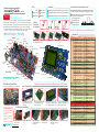
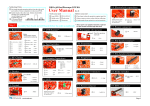
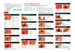
Panel & Connectors
Power switch, Menu,
& Parameter Adjustment
Sensitivity
Selector 2
Hold/Run
(SW3)
Basic Operations
1. Connection
2. Power on & off
Connect probe to the BNC connector marked "INPUT" (Fig 4). Connect USB cable if the unit
is powered by USB (Fig. 2).
Power ON: Press [ADJ] dial once. System will first enter Bootloader, stay for about 2 seconds,
and then enter running state.
Power OFF: Hold [ADJ] dial for about 3 seconds.
3. Set parameters
Oscilloscope parameters can be grouped by three main catagories: vertical, horizontal, and trigger.
1 ) Vertical --- including SENSITIVITY, POSITION, and COUPLE.
To set SENSITIVITY use the upper two slide switches. Setting is displayed on screen as "volt/div".
To change vertical POSITION press [VPOS] button and then turn [ADJ] dial.
To change COUPLE use the lower slide switch
Sensitivity
Selector 1
(SW2)
Couple
Selector
USB Socket
(SW1)
Fig. 1
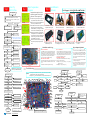
Trigger Level
External Battery
Connector
Fig. 2
Parameter Selection
HOLD Indicator
2 ) Horizontal --- including TIMEBASE and POSITION
To set TIMEBASE press [ Sec/Div] button and then turn [ADJ] dial.
To change horizontal POSITION press [HPOS] and then turn [ADJ]. Setting is diaplayed as "Second/div" on screen.
3 ) Trigger --- including trigger MODE, SLOPE, and LEVEL
To set trigger MODE press [MODE] button and then turn [ADJ] dial
To set trigger SLOPE press [SLOPE] button and then turn [ADJ] dial
To change trigger LEVEl press [LEVEL] button and then turn [ADJ] dial
Couple
What Trigger Mode Means and How to Use It
Sensitivity
Vertical
Position
The trigger can work under automatic (AUTO). normal ( NORM), or single (SING) mode. Under AUTO mode the scope
will perform capture and display results no matter there is trigging or not. Under NORM mode the scope performs capture
and updates display only when trigging happens. The SING mode is similar to NORM mode. The only difference is under
SING mode the scope will enter HOLD state automatically after a capture and will stay untill manual release.
(V/Div)
Timebase (Sec/Div)
Ver. & Hor.
Adjustment
When trigger mode is set to NORM or SING you may find no screen updates. This is because there is no trig happening.
In this case you may like first switch to AUTO mode to make sure signal and trigger level are in proper range and then
switch back to NORM or SING.
Trigger Mode
Trigger Level
Fig. 3
Hor. Position
Trig Point
Test Signal
(Freq. variable)
Trigger Slope
Signal Input
Fig. 4
1. Press [ADJ] to have menu displayed.
2. Turn [ADJ] to select function and press [ADJ] to execute.
Button Functions
Botton functions are mode dependent. Please
see their function under different modes below.
Menu Operations
Under any mode:
[ADJ] hold - power off, [LEVEL] hold - backlight ON/OFF
Menu Functions
No.
1. Oscilloscope Mode
RUNNING
Menu Item
Function Descriptions
0
1
2
3
OSCILLOSCOPE
FREQ METER
FFT
SAVE WAVEFORM
Enter oscilloscope mode
Enter frequency meter mode
Enter FFT mode
Save waveform. The last waveform captured before enter menu is saved to EEPRON.
(This function is only available under oscilloscope mode)
Button Name
[VPOS]
Function
Select vertical position
[HPOS]
Select horizontal position
Button Name
[VPOS]
[SEC/DIV]
Select timebase
[HPOS]
RECALL WAVEFORM
Select trigger mode
[MODE]
Select horizontal position
Select trigger mode
4
[MODE]
Recall saved waveform from EEPROM and display it in HOLD state.
(This function is only available under oscilloscope mode)
[SLOPE]
Select trigger slope
[ADJ] ratating
Adjust parameter selected
5
SEND SCREEN
[LEVEL]
Select trigger level
[ADJ] press
Enter MENU
Send screen as bitmap file via serial port. The screen right before entering menu will be
sent. XModem protocol is used for the transfer. Refer to documents at www.jyetech.com.
[HOLD]
Return to running
6
SEND WAVE DATA
Send waveform data as CSV file via serial port. The displayed waveform right before
entering menu will be sent. XModem protocol is used for the transfer.
7
CHANGE REC. LEN
Select record length by turning [ADJ]. Record length can be set to 256, 512, or 1024.
8
CHANGE TRIG POS
Select trigger position by turning [ADJ]. Trigger position can be set to 1% - 100% of
capture buffer.
9
TEST SIGNAL
Set the frequency and amplitude of test signal. Use [ADJ] to change frequency. Press
[LEVEL] to select amplitude.
10
RESTORE DEFAULT
Reset parameters to factory defaults. See the table in next page for affacted parameters.
11
REBOOT
Reboot device (usually to enter bootloader for firmware upgrading ).
12
EXIT
Exit menu and return to previous state.
[HOLD]
Enter HOLD
[ADJ] ratating
Adjust parameter selected
[ADJ] press
Enter MENU
[VPOS] hold
Align vertical position
Sen. selector 1
Change sensitivity
Sen. selector 2
Change sensitivity
Couple selector
Change couple
2. Frequency Meter Mode
HOLD
Function
Select vertical position
MENU
Button Name
Function
[ADJ] ratating
Select menu item
[ADJ] press
Execute the item selected
3. FFT Mode
Button Name
Function
Button Name
Function
[ADJ] press
Enter MENU
[ADJ] press
Enter MENU
[HPOS]
Select FFT size
Sen. selector 1
Change sensitivity
Sen. selector 2
Change sensitivity
[SEC/DIV]
[ADJ] ratating
Select FFT sampling rate
Adjust parameter selected
Couple selector
Change couple
JYE Tech Ltd.
- www.jyetech.com -
Advanced Operations
Firmware Upgrading
10X Probe Calibration
Due to input capacitance 10X probe must be calibrated for correct amplitude dispaly.
The calibration can be perform by use of the built-in test signal generator of 068.
Test signal output
1 ) Enter menu. Set test signal to 1KHz and 5V respectively .
2 ) Set the switch on probe handle to "10X" position.
3 ) Set timebase to 0.2ms and sensitivity to 0.2V (see Fig. 6).
4 ) Place probe tip onto the central conductor of test signal connector
(Fig. 5). Adjust trigger level if display is not stable.
5 ) Adjust the cap trimmer at probe connector with small .screw driver
(see Fig. 5) so as sharp rectangle waveform is displayed (middle
screen of Fig. 6).
Fig. 5
Cap trimmer
Fig. 6
Not enough
Good
Too much
Vertical Position Alignment
In case of that there is a mismatch between 0V trace and the vertical position indicator please follow
the steps below to eliminate it.
1 ) Set couple switch to GND position.
2 ) Hold [VPOS] for about 3 seconds. You should see the 0V trace aligned to the indicator.
USB Connection
www.silabs.com/products/mcu/pages/usbtouartbridgevcpdrivers.aspx
Serial Port Parameters
For the main firmware serial port parameters are fixed to 115200 bps and 8-N-1.
For the bootloader serial port parameters are fixed to 9600 bps and 8-N-1.
Use XModem supporting software(such as Tera Term) for uploading. Name screen image to "bmp"
file. Name waveform data to "csv" file. First start sending from menu and then start receiving at
host. Note that the screen or waveform displayed right before entering menu will be sent.
Boot Process and Indication
At powering-up or reset system first enters bootloader (bootloader is installed before shipment).
LED D1 will flash once. If jumper JP7 is closed buzzer will beep once accordingly. System will
stay in bootloader for about 2 seconds detecting firmware upgrading request from host. If no
request received it will enter the main firmware.
Once in the main firmware JYE Tech logo will be displayed together
with firmware versions. LED D1 will flash twice. If jumper JP7 is
Factory Default
closed buzzer will beep twice accordingly. System then enters
1ms/DIV
Timebase
working state.
0
Vertical Pos
The activities of LED and buzzer serve as indication of correct booting.
Horizon. Pos 80
Normally factory default can be recovered by menu. It can also be done
by connecting PF6 (at J7) to ground and performing reset (press SW12
for example). Remember to disconnect PF6 from ground after recovery
is done.
JYE Tech Ltd.
- www.jyetech.com -
Use Battery
High byte 0xC2
Low byte 0x2E
U5(ATmega48) Fuse Bits
Ext. byte 0xFF
High byte 0xD6
Low byte 0xE2 ("F" PCB)
0xE0 ("H" PCB)
Equivalent-Time Sampleing (ETS)
Screen Image & Waveform Data Upload
Trigger Mode
Trigger Slope
Trigger Pos
Record Len.
Test Sig. Freq.
Test Sig. Amp.
Fuse Bits Setting
It is important to have correct fuse bit setting for DSO 068 to run
normally. The factory fuse setting for U4 and U5 are listed in tables
at right. Please do not change them unless you know what you are doing.
DSO 068 can be powered by battery. Typically 3.7V/1200mAh Li-ion battery is used. When fully
charged it can run the device about 4 hours with backlight on.
The assembly BOB2 (JYE118) is battery/USB power switch and battery charger. It charges battery
once USB is connected. The charging process is fully automatical and terminates itself when
battery is full. The charge current can be programmed by R32. Please refer to datasheet of JYE118
for details.
Short JP5 if external battery is to be used. Note: Internal battery must be removed in this case.
In order to use USB function the host which DSO 068 is to communicate with is required
to install driver supporting the USB-Uart bridge CP2102. Please use the following link
to download driver and install it (refering to documents accompanying).
Forced Default Recovery
DSO 068 contains two AVR microcontrollers from Atmel: ATMega64 (U4) and ATMega48 (U5).
Their function and performance can be changed by changing firmware.
Note that the firmware of U4 can be changed by programmer or bootloader. Firmware of U5 can
only be changed by programmer.
J4 and J5 pinout
By Programmer
The program ports for U4 and U5 are J4 and J5 respectively. Their
GND GND
+5V
pinout is compatible to STK200 and is shown in Fig. 7. It is
important to pick up a programmer with matching programming
Pin 1
header. JYE Tech offers compatible programmer (PN: 07302).
Follow instructions of selected programmer and host application
MOSI SCK nRST MISO
to perform firmware upgrading.
Fig. 7
By Bootloader
DSO 068 has bootloader pre-installed which can work with an PC application via serial connection
to perform firmware upgrading. The PC application is called AVRUBD. It can be downloaded at
http://www.jyetech.com/Support/avrubd.rar
For how to use bootloader please refer to the aritcle "How to Upgrade Firmware by Bootloader"
(http://www.jyetech.com/Support/HowToUpgradefirmwareByBootloader.pdf).
DSO 068 can enter bootloader by one of three methods: 1 ) powering-up;
U4(ATmega64) Fuse Bits
Ext. byte 0xFF
2 ) executing menu item REBOOT; 3 ) pressing switch SW12.
AUTO
Falling
50%
256 points
1000Hz
5V
When timebase is set to 2us or faster capture will automatically use Equivalent-Time Sampling
method. This method can display more details
of signal. But there are two conditions for it
Specifications
to work:
Max ETS sampling rate
20MSa/s
1 ) Signal must be periodic.
Max realtime sample rate 2MSa/s
2 ) Trig must happens.
Analog bandwidth
0 -- 3MHz
As a result in ETS you may see no screen
Sensitivity range
10mV/div - 5V/div
activity if any of these conditions are not
Max input voltage
50Vpk (1X probe), 400Vpk(10X probe)
met. In this case try adjusting trigger level
Input impedance
1M ohm/20pF
to make trig happen.
Resolution
8 bits
Record length
256,512,1024 points (variable)
Note that trig point has no meaning in ETS.
Data Interface
The data interface of DSO 068 is a serial
interface of Uart (TTL level) or USB. It has
two main functions:
1 ) Working with jyeLab as USB Scope.
2 ) High resolution (10 bits) Data Logger.
Details of the data interface are separately
documented.
Timebase range
Trigger modes
Trigger position range
Frequency meter range
F. meter sensitivity
Power supply
Current consumption
Dimension
Weight
10m(minute)/Div -- 0.5us/Div
Auto, Normal, and Single
0% -- 100%
5MHz
0.2Vpp @ 5MHz
3.7V Li-ion batter / USB
~300mA (with LCD backlight ON)
140 x 70 x 30mm
~0.18KG (without battery and probe)
DSO 068 Oscilloscope DIY Kit
Tools
Get Ready
Soldering Skills and Requirements
Assembly Guide
1 Iron (20W) 4 Screw driver
2 Solder wire 5 Flush cutter
3 Multimeter 6 Tweezers
1 Check part values & quantities against part list
2 Meter and identify resistor values by ohm meter
3 Understand all part polarities and orientations
1 Put leads through mounting from installation side of
PCB. Ensue they evenly touch PCB (picture below).
2 Solder at the other side of PCB. Solder should fully
fill and cover soldering pads.
Avoid bridges with
neighbering pads.
3 Cut unused leads
flush with cutter.
Rev F01
Step 1 AssemblyMain Board
1. Complete the steps in "Get Ready" and understand soldering requirements.
2. Install parts by the order of part list. Start from the back side of main board.
3. Pay special attention to part polarity at soldering. Refer to photos to the right.
4. For BOB boards and LCD soldering refer to photos at bottom for details.
5. After all back side parts are finished perform powering-up test as explained
+
Identify
Polarity &
Orientation
+
Diode
at the reverse page. Continue rest installation if test result is good.
TIP: Resistor values are easily mis-read.
Ohm meter check is strongly suggested.
-
LED
+
-
Electrolytic cap.
E
B C
Transistor
TIP: C3 and R32
are not required.
Part List
USB-Uart
Buzzer
Step-up Convertor
Reset
USB Socket
Neg. P.S.
Convertor
LED
JYE116( BOB4)
JYE117(BOB3)
(Pin 1 indicated by arrow)
JYE118(BOB2)
JYE119 ( BOB1)
JYE120(BOB5)
Rotary Encoder
Charger
Diode Inductor
Electrolytic Cap.
On/Off Switch
Front Side
Resistor
Ceramic Cap.
External
Batt.
Battery
Cap. Trimmer
Test Signal
Crystal
LCD Contrast
Back Side
MCU
Extention Ports
Transistor
TIP: Do not install J4 & J5. They can be inserted
into programmer header at programming.
A/D Converter
Slide Switch
LCD Module
CBB Cap
Important! Unused leads under LCD must be cut flush to avoid short to LCD module!
BOB Boards Installation
LCD Installation
Pin 1 location indicated by arrow (square pad)
ASSY2 ASSY 3
L abels
Cut leads sh ort
under LCD
ASSY1
A.
Lay PCB flat. Insert mounting strips with longer pins
into holes.
BOBs and Jumpers
B.
C.
Identify the holes with labels
on LCD. They should go
with the long strip.
D.
Put LCD onto strips as shown.
Solder pins at corners first. Do
the rest after flatness ensured.
Turn LCD and main boar over.
Complete soldering following
same procedures as in C.
BOB Board Installation
Keep JP1 open if BOB2
is installed. Otherwise
short it.
Keep JP2 open if BOB3
is installed. Otherwise
short it.
A. Use the small acrylic B. Apply solder to one C. Apply solder to the D. Put BOB to place
More at the reverse page
tool provided.
pin.
corresponding pin on
and align pads.
main PCB.
JYE Tech Ltd.
- www.jyetech.com -
Note: Please install by the order given in the Part List below.
E. Maintain BOB upright F. Finish the rest pins.
and fix it by melting
the solder.
Catagory
Seq.
Main PCB
Resistor
1
2
3
4
5
6
7
8
9
10
11
12
13
14
15
16
17
18
19
20
21
22
23
24
Switch
Connector
Wire
Screw
Acrylic
46
47
48
49
50
Type/Spec
101-06802
510KΩ ,5%, 1/8W
200KΩ ,1%, 1/8W
2MΩ ,1% ,1/8W
20KΩ ,1% ,1/8W
300Ω ,1% ,1/8W
180Ω ,1% ,1/8W
120Ω, 1%, 1/8W
3.3KΩ ,1%,1/8W
470Ω ,1% ,1/8W
0Ω ,5 %, 1/8W
10KΩ ,1 %,1/8W
1KΩ ,5% ,1/8W
10MΩ, 5 %, 1/8W
1N4148,DO-35
Qty
1
2
1
2
1
2
1
2
2
3
1
4
5
1
2
3
1
1
1
2
1
1
2
12
Designator/Location
R1, R27
R3
R2, R4
R5
R6, R23
R7
R8, R12
R10, R22
R11, R31, R 33
R13
R9, R21, R20,R30
R24,R25,R26,R28,R29
R40
D2,D3
Diode
100uH, φ2.5 X 6mm
L1,L4,L5
Inductor
20MHz,HCM-49
Y1
Crystal
Connector
USB socket, MiNi- B type
J1
Switch
Tact, 6 X 6 X 5mm
SW12
300pF, ceramic disk
C2,C23
Capacitor
C4
3pF, ceramic disk
1pF, ceramic disk
C6
120pF, ceramic disk
C7, C13
0.1uF, ceramic disk
C9,C10,C11,C12,C14,
C15,C16,C18,C20,C24,
C25,C26
25 15pF, ceramic disk
2 C21,C22
1 C1
26 0.1uF/100V, CBB
1 BP1
Buzzer
27 5V, passive, φ9 X 5.5mm
1 D1
28 LED, φ3mm , red
Diode
2pins, 2.54mm
2 J6, J10
Connector 29
Transistor 30 8550, TO-92 ( E-B-C)
2 Q1, Q2
1 C19
Electro.
31 10uF,16V, φ4 X 5mm
Capacitor 32 100uF,16V, φ6X 7mm
5 C17,C27,C28,C29,C30
1 J2
Connector 33 DC005, φ2.1 mm core
1 BOB4
BOB
34 JYE116, step-up convertor
Board
35 JYE120, neg. P.S. convertor
1 BOB5
36 JYE117, On/Off switch
1 BOB3( optional)
37 JYE118, battery charger
1 BOB2( optional)
38 JYE119,UART-USB conv.
1 BOB1( optional)
Now perform power-up test. See steps at the reverse page.
Continue following assembly after test.
39 Slide switch ,SS-23D 06
3 SW1,SW2,SW3
Switch
Switch
1 SW4
40 Rotary Enc., EC11, 10mm
1 ASSY1
41 SIP, 2mm, 20X1
Pin
Strip
SIP,
2mm,
2X1
2
ASSY2,ASSY3
42
LCD
43 128X64 graphic , 12864-16 1 LCD1
2 J4,J5(Do not install)
Pin strip
44 DIP,2.54mm,5X2
Enclosure 45 Top(1), bottom(1), stand(1) 1 set
switch caps(3), dial cap(1)
7-key silicone button pad
BNC,BNC-KY
2-core hood-up wire, 10cm
2.3*8mm, self tapping
Tool for holding BOB
1
2
1
4
1
Adjust Compensation
Power Up
Step 2 the First Time
Double check to ensure no missed, cold solder or shorts
Make sure BOB4 and BOB5 have been installed
Close JP2 for the time being (even BOB3 is in place)
Keep JP3、JP4 open
Power off. Close JP4
Power up and check +5V
again. Is it still +5V?
*
*
Yes
Press buttons. Do you see
reaction on screen ?
通电检查
Check for soldering mistakes.
Wrong polarity, shorts, etc.
LED reversed ?
U4 pin 20 voltage low ?
Check Y1、C21、C22
No
too much
No
Follow "No display"
flowchart to check
No
Check U5 and soldering
of button related pins
Scope
Input
Yes
Set cursor to timebase. Turn No
[ADJ] dial. Do you see
timebase change ?
Check U5 and soldering
of rotary encoder pins
Is V- normal (-5V) ?
Yes
Is AV- normal (-5V) ?
Yes
Is VA normal (+5V) ?
Is V3 measured 0V?
Yes
is V4 measured ~1.6V?
No
No
No
are done.
Major Jumpers Explained
JP1:This by-pass of charger BOB2. If battery
We want to check the connection between U3 pin12 and
U4 pin17, for example. First enter Check Mode as stated
earlier. Measure voltage at U3 pin12 with a volt meter. If
voltage change between 0V and 5V is observed the connection is good. Otherwise is bad.
is not used (as result, no BOB2) keep JP1 closed.
JP2:This is by-pass of switch BOB3. If BOBs
is not used JP2 should be closed. In order to focus
on the main circuit we temporarily close JP2 at
power-up test even BOBs is installed. It is kept
open after test.
"Check Mode" Related Pins
How to Enter "Check Mode"
Close JP6 and power up the system. It will anter "Check
Mode". You should see LED flashes at about 3 second
cycle.
Remember restore JP6 to open after checking.
Not all pins have the Check Mode function. The pins
that do are listed as following:
JP3:This is by-pass of step-up converter BOB4.
U4:PB[7:5, 3:0],PC[7:0],PD[7, 5, 3, 1, 0],PE[7:3],
JP4:This is the connecting point of power supply
Usually JP3 is kept open.
PF[7:0],PG[4:0]
and the rest circuits. For the safety of the rest
circuit only close JP4 after power supply is
tested good.
U5:PB[5:1], PC[3:0],PD[7, 6, 4:1]
Check BOB5 and C27
+5V
(+5V)
JP4
JP7
Check USB
JP6
V-
JP8
(+5V)
AV+
V5
(~1.6V)
Is VBUS measured ok?
No
AV-
Check D4
(-5V)
Yes
Check L5, C16, and C17
V2
Check BOB4
No
No
Check JP2
Yes
Is +5V measured ok ?
*
(0V )
Check BOB2
Is voltage at LCD No Check related
pin 19 5V?
connections
Yes
Short C and E of Q2.
Does LCD light up?
No Possible LCD
issue
Yes
BOB3 installed ?
Yes
No
No
Check batt.
Yes
Is VS+ measured ok ?
*
(0V )
USB
Connector
Is V+ measured ok ?
Yes
V3
(About +5V)
No
Battery voltage ok ?
Yes
Is V+ measured ok ?
VBUS
Check L1, C28, C11, and C12
LCD Dark
Battery powered
No
*
(-5V)
JP3
USB powered
in photo below) and (+) pole at points of measurement.
" are measured when SW1 (couple) is placed at GND position.
Check L4, C29, C9, and C10
Check Q2, R30 and
connection with U5
Check BOB3
Yes
Power good
*
No
No
No
Check SW1, SW2, and R1
VB
V+
(0.6V)
JP1
VT
JP2
V1
Check SW3, R9, R10, R11
Follow "No Trace"
flowchart to check
Yes
Powered by USB: V+ ≈VBUS - 0.7V
Powered by Batt.: V+ ≈ VBAT
- www.jyetech.com -
*
(0V )
JP5
VA
(+5V)
VBAT
No
Press SW12. Does LED blink as it should be ?
Battery
Connector
VS+
Reference point for
voltage measurement
SYSCLK
(2.5V)
Contrast Adj.
LCD pin18
(About -5V)
Without BOB3:VS+ = V+ (due to JP2 closed)
With BOB3:VS+ depends on state of BOB3 (On or Off)
Signal Input
Yes
Ensure all analog voltages
are normal (see photo)
VT and VB normal?
No
Yes
(Battery voltage)
(Volt. range: 2 - 5V)
No Display
No Trace
(2.6V)
U1 may have been damaged
Yes
JYE Tech Ltd.
H. Put dial cap on and you
the two screws as shown.
Use of "Check Mode"
V4
(~1.6V )
Adjust VPOS. Can you see No
trace displayed ?
Scope is
wor king now
to main board as shown.
G. Put on back cover. Tight
Avoid high parts (J10, C30).
Check Mode is to assist connection checking for most
MCU pins. Once in Check Mode MCUs will generate
high and low levels at those pins. These levels can be
easily checked with a volt meter and consequently find
out pin connections. This is particularly useful for
checking out suspecious SMD solderings.
Set SW1, SW2, SW3 to GND,
10mV, and X1 respectively
Yes
F. Attach batt. to back cover.
1. All voltages are measured with volt meter's (-) pole at reference point (indicated
2. Voltages with "
No
Yes
Is V2 measured 0V?
D. Connect BNC connectors
USB end and push in.
No Power
Check Analog Part
Yes
C. Hold board tight towards
board to connector holes.
Troubleshooting
TIP: If JP7 is closed you will
here beeps while LED blinks
Notes:
Is AV+ normal (+5V) ?
B. Cap slide switches. Insert
What is "Check Mode"
Connect test signal output to scope input temporarily
Yes
Now the digital
part is working
AIN: 上
AGND:下
Check Mode and Its Usage
C5
C8
Follow "LCD Dark"
flowchart to check
Yes
Adjust contrast. Can you
see display?
通电检查
front side parts if r eached here
Press SW12. Do you see LED No
blink once (if bootloader
installed) and then twice ?
LCD backlight on ?
Good
( )You can continue to install
Yes
Yes ( )
Not enough
Follow "No Power"
flow chart to check
No
1
通电检查
Yes
红:上
黑:下
2
(see photo below) and set SW1 to DC.
2. Power up. Set test signal to 10KHz and
5V. Set scope timebase to 20us.
3. Set SW & SW3 to 1V & X2 respectively. A. Install BNC connectors
Adjust trigger level to make display
and place silicone pad.
stable if necessary. Change C8 to obtain
waveform as the middle of photos left.
4. Keep signal frequence unchanged and
set amplitude to 1V. Set SW2 & SW3 to
0.1V and X5 respectively. Make display
stable. Change C5 to obtain waveform
as the middle of photos left.
5. Remove connection between test signal
output and scope input. Adjustment is
E. Tight two screws as
done.
indicated by arrows.
Keep JP1 open
Make sure BOB2 in
No
Power up. Check voltage
at +5V test point. Is it +5V?
Tech Support: www.jyetech.com/forum
1. Connect test signal output to scope input
Battery powered
Close JP1 if no BOB2
Step 4 Enclosure
Compensation capacitors can be
adjusted using the built-in signal
generator. Follow steps below:
Powering-up Test
USB powered
Install Batter &
Step 3 Capacitors
Connection between U4
pin17 and U3 pin12 good ?
Yes
U3 has bad soldering
or has been damaged
Is contrast changeable by POT1?
No
Yes
U3 damaged
No
Check out
the cause
Yes
LCD defective
Volt. at LCD pin18 negative?
Yes
Check all connections between
U4 and LCD for opens or shorts.
U4 and LCD connection good ?
Check Y1, C21, C22
Volt at U4 pin20 too low ?
Re-program U4
Check POT1 and related
No
Eliminate bad connections
No