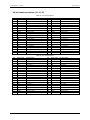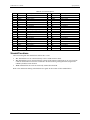
1
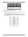
USB-2623 Analog Input and Digital I/O Measurement and Control User's Guide Document Revision 3 July 2014 © Copyright 2014 Your new Measurement Computing product comes with a fantastic extra — Management committed to your satisfaction! Thank you for choosing a Measurement Computing product—and congratulations! You own the finest, and you can now enjoy the protection of the most comprehensive warranties and unmatched phone tech support. It’s the embodiment of our mission: To provide data acquisition hardware and software that will save time and save money. Simple installations minimize the time between setting up your system and actually making measurements. We offer quick and simple access to outstanding live FREE technical support to help integrate MCC products into a DAQ system. Limited Lifetime Warranty: Most MCC products are covered by a limited lifetime warranty against defects in materials or workmanship for the life of the product, to the original purchaser, unless otherwise noted. Any products found to be defective in material or workmanship will be repaired, replaced with same or similar device, or refunded at MCC’s discretion. For specific information, please refer to the terms and conditions of sale. Harsh Environment Program: Any Measurement Computing product that is damaged due to misuse, or any reason, may be eligible for replacement with the same or similar device for 50% of the current list price. I/O boards face some harsh environments, some harsher than the boards are designed to withstand. Contact MCC to determine your product’s eligibility for this program. 30 Day Money-Back Guarantee: Any Measurement Computing Corporation product may be returned within 30 days of purchase for a full refund of the price paid for the product being returned. If you are not satisfied, or chose the wrong product by mistake, you do not have to keep it. These warranties are in lieu of all other warranties, expressed or implied, including any implied warranty of merchantability or fitness for a particular application. The remedies provided herein are the buyer’s sole and exclusive remedies. Neither Measurement Computing Corporation, nor its employees shall be liable for any direct or indirect, special, incidental or consequential damage arising from the use of its products, even if Measurement Computing Corporation has been notified in advance of the possibility of such damages. Trademark and Copyright Information Measurement Computing Corporation, InstaCal, Universal Library, and the Measurement Computing logo are either trademarks or registered trademarks of Measurement Computing Corporation. Refer to the Copyrights & Trademarks section on mccdaq.com/legal for more information about Measurement Computing trademarks. Other product and company names mentioned herein are trademarks or trade names of their respective companies. © 2014 Measurement Computing Corporation. All rights reserved. No part of this publication may be reproduced, stored in a retrieval system, or transmitted, in any form by any means, electronic, mechanical, by photocopying, recording, or otherwise without the prior written permission of Measurement Computing Corporation. Notice Measurement Computing Corporation does not authorize any Measurement Computing Corporation product for use in life support systems and/or devices without prior written consent from Measurement Computing Corporation. Life support devices/systems are devices or systems that, a) are intended for surgical implantation into the body, or b) support or sustain life and whose failure to perform can be reasonably expected to result in injury. Measurement Computing Corporation products are not designed with the components required, and are not subject to the testing required to ensure a level of reliability suitable for the treatment and diagnosis of people. HM USB-2623.docx 2 Table of Contents Preface About this User's Guide ....................................................................................................................... 5 What you will learn from this user's guide ......................................................................................................... 5 Conventions in this user's guide ......................................................................................................................... 5 Where to find more information ......................................................................................................................... 5 Chapter 1 Introducing the USB-2623 .................................................................................................................... 6 Functional block diagram ................................................................................................................................... 7 Chapter 2 Installing the USB-2623 ........................................................................................................................ 8 What comes with your shipment? ....................................................................................................................... 8 Hardware .......................................................................................................................................................................... 8 Software ............................................................................................................................................................................ 8 Documentation .................................................................................................................................................................. 8 Optional components ........................................................................................................................................................ 8 Unpacking........................................................................................................................................................... 8 Installing the software ........................................................................................................................................ 8 Installing the hardware ....................................................................................................................................... 9 Configuring the hardware ................................................................................................................................... 9 Calibrating the hardware..................................................................................................................................... 9 Field calibration ................................................................................................................................................................ 9 Factory calibration ............................................................................................................................................................ 9 Chapter 3 Signal Connections .............................................................................................................................10 68-pin SCSI connector P1 ................................................................................................................................ 10 Cabling.............................................................................................................................................................................11 Signal termination ............................................................................................................................................................11 40-pin header connectors J2, J4, and J5............................................................................................................ 12 Cabling.............................................................................................................................................................................13 Signal termination ............................................................................................................................................................13 Chapter 4 Functional Details ...............................................................................................................................14 Analog input modes .......................................................................................................................................... 14 Software paced .................................................................................................................................................................14 Hardware paced ...............................................................................................................................................................14 Burst mode........................................................................................................................................................ 14 USB-2623 components ..................................................................................................................................... 15 68-pin SCSI connector P1 ................................................................................................................................................15 40-pin header connectors J2, J4, and J5 ...........................................................................................................................16 USB connector .................................................................................................................................................................16 LEDs ................................................................................................................................................................................16 Standoffs ..........................................................................................................................................................................16 Signal descriptions ............................................................................................................................................ 16 Analog input ....................................................................................................................................................................16 Digital I/O ........................................................................................................................................................................16 Counter input ...................................................................................................................................................................18 Trigger input ....................................................................................................................................................................18 Timer output ....................................................................................................................................................................18 Ground .............................................................................................................................................................................18 Power output ....................................................................................................................................................................18 USB power ....................................................................................................................................................... 18 3 USB-2623 User's Guide Mechanical drawing ......................................................................................................................................... 19 Chapter 5 Specifications ......................................................................................................................................20 Analog input ..................................................................................................................................................... 20 Accuracy ........................................................................................................................................................... 20 Analog input DC voltage measurement accuracy ............................................................................................................20 Noise performance ...........................................................................................................................................................21 Settling time for multichannel measurements ..................................................................................................................21 Analog input calibration ................................................................................................................................... 21 Digital input/output........................................................................................................................................... 21 External trigger ................................................................................................................................................. 22 External clock ................................................................................................................................................... 22 Counter ............................................................................................................................................................. 22 Timer output ..................................................................................................................................................... 23 Memory ............................................................................................................................................................ 23 Power ................................................................................................................................................................ 23 USB .................................................................................................................................................................. 24 Environmental .................................................................................................................................................. 24 Mechanical ....................................................................................................................................................... 24 Signal connections ............................................................................................................................................ 24 68-pin SCSI connector (P1) .............................................................................................................................................25 40-pin header connectors (J2, J4, J5) ...............................................................................................................................26 Standoff locations ............................................................................................................................................. 27 4 Preface About this User's Guide What you will learn from this user's guide This user's guide describes the Measurement Computing USB-2623 data acquisition device and lists device specifications. Conventions in this user's guide For more information Text presented in a box signifies additional information related to the subject matter. Caution! Shaded caution statements present information to help you avoid injuring yourself and others, damaging your hardware, or losing your data. bold text Bold text is used for the names of objects on a screen, such as buttons, text boxes, and check boxes. italic text Italic text is used for the names of manuals and help topic titles, and to emphasize a word or phrase. Where to find more information For additional information relevant to the operation of your hardware, refer to the Documents subdirectory where you installed the MCC DAQ software (C:\Program Files\Measurement Computing\DAQ by default), or search for your device on our website at www.mccdaq.com. 5 Chapter 1 Introducing the USB-2623 The USB-2623 is a USB 2.0 high-speed device that is supported under the Microsoft® Windows® operating system. The USB-2623 is compatible with both USB 1.1 and USB 2.0 ports. The speed of the device may be limited when using a USB 1.1 port due to the difference in transfer rates on the USB 1.1 versions of the protocol (lowspeed and full-speed). The USB-2623 device provides the following features: 16 single-ended (SE) analog inputs 24 DIO channels; bit configurable for input or output Four counter inputs Four timer outputs Digital trigger input External AI scan clock input External AO scan clock input One 68-pin SCSI connector and three 40-pin header connectors for field wiring connections The USB-2623 is powered by the USB supply from the computer; external power is not required. 6 USB-2623 User's Guide Introducing the USB-2623 Functional block diagram USB-2623 functions are illustrated in the block diagram shown in Figure 1. Figure 1. USB-2623 functional block diagram 7 Chapter 2 Installing the USB-2623 What comes with your shipment? Verify that the following hardware components are included in the shipment: Hardware USB-2623 (with standoffs) USB cable Software MCC DAQ CD Documentation MCC DAQ Quick Start Guide The Quick Start Guide booklet provides an overview of the MCC DAQ software you received with the device, and includes information about installing the software. Please read this booklet completely before installing any software or hardware. Optional components Cables o CA-68-3R o C40FF-x Signal termination boards o TB-100 o TB-103 o CIO-MINI40 Unpacking As with any electronic device, you should take care while handling to avoid damage from static electricity. Before removing the USB-2623 from its packaging, ground yourself using a wrist strap or by simply touching the computer chassis or other grounded object to eliminate any stored static charge. If any components are missing or damaged, contact us immediately using one of the following methods: Knowledgebase: kb.mccdaq.com Phone: 508-946-5100 and follow the instructions for reaching Tech Support Fax: 508-946-9500 to the attention of Tech Support Email: [email protected] For international customers, contact your local distributor. Refer to the International Distributors section on our website at www.mccdaq.com/International. Installing the software Refer to the Quick Start Guide for instructions on installing the software on the MCC DAQ CD. This booklet is available at www.mccdaq.com/PDFmanuals/DAQ-Software-Quick-Start.pdf. 8 USB-2623 User's Guide Installing the USB-2623 Installing the hardware Install the software before you install your device A driver needed to run the USB-2623 is installed when you install the software. Therefore, you need to install the software package you plan to use before you install the hardware. For operation on a Windows operating system, we recommend that you run Windows Update to update your operating system with the latest USB drivers. To connect a USB-2623 device to your system, turn on your computer and connect the USB cable to an available USB port on the computer or to an externally powered USB hub connected to the computer. When connected for the first time, a Found New Hardware dialog opens when the operating system detects the device. When the dialog box closes, the installation is complete. The Power LED (top LED) blinks during device detection and initialization, and then remains on. When the board is first powered on, there is usually a momentary delay before the Power LED blinks or turns on. Configuring the hardware All hardware configuration options are programmable with software. Caution! Avoid redundant connections. Ensure that there is no signal conflict between the 68-pin SCSI connector (P1) and the 40-pin connectors (J2 to J5). Failure to do so could possibly cause equipment damage and/or personal injury. Turn off power to all devices connected to the system before making connections. Electrical shock or damage to equipment can result even under low-voltage conditions. Always handle components carefully, and never touch connector pins or circuit components unless you are following ESD guidelines in an appropriate ESD-controlled area. These guidelines include using properly-grounded mats and wrist straps, ESD bags and cartons, and related procedures. Avoid touching board surfaces and onboard components. Only handle boards by their edges. Make sure that the USB-2623 does not come into contact with foreign elements such as oils, water, and industrial particulate. The discharge of static electricity can damage some electronic components. Semiconductor devices are especially susceptible to ESD damage. Calibrating the hardware Field calibration The USB-2623 supports self-calibration. Run the InstaCal utility to calibrate the USB-2623 whenever the ambient temperature changes by more than ±10 °C from the last self-calibration. The recommended calibration interval is one year. Calibrate the inputs before calibrating the outputs. Factory calibration The Measurement Computing Manufacturing Test department performs the initial factory calibration. Return the device to Measurement Computing Corporation if you want the factory calibration restored. 9 Chapter 3 Signal Connections Board signals are available on the 68-pin SCSI connector P1 and 40-pin header connectors J2, J4, and J5. Caution! Avoid redundant connections! Make sure there is no signal conflict between the SCSI connector pins and header connector pins. Failure to do so could possibly cause equipment damage and/or personal injury. Use the SCSI cable for optimal analog input settling time To achieve the best analog input channel-channel settling time performance, connect your signals to the SCSI connector (P1). If the J2 to J5 connectors are to be used, keep the interface cable as short as possible to minimize settling errors. 68-pin SCSI connector P1 The SCSI connector provides connections to the board signals listed in Figure 2. Figure 2. SCSI connector P1 pinout 10 USB-2623 User's Guide Signal Connections Cabling Use a CA-68-3R cable (Figure 3) when connecting signals to the SCSI connector. Figure 3. CA-68-3R cable Signal termination TB-100 – screw terminal board that connects to SCSI connector P1 with a CA-68-3R cable. A 19-inch rack mount kit (RM-TB-100) is also available. The following table lists how TB-100 screw terminals are mapped to the SCSI connector pins. TB-100 to SCSI connector pin map TB2 terminal SCSI pin TB1 terminal SCSI pin +5V GND A0 A1 A2 A3 A4 A5 A6 A7 B0 B1 B2 B3 B4 B5 B6 B7 C0 C1 C2 C3 C4 C5 C6 C7 TTL TRG GND CNT0 CNT1 CNT2 19 GND 18 52 17 51 16 50 15 49 14 48 13 47 12 46 11 45 10 44 9 43 8 42 7 41 6 GND 5 39 4 ACH0 ACH8 AGND ACH1 ACH9 AGND ACH2 ACH10 AGND ACH3 ACH11 AGND ACH4 ACH12 AGND ACH5 ACH13 AGND ACH6 ACH14 AGND ACH7 ACH15 XDAC3 (Note 1) SGND NC (Note 2) XDAC2 (Note 1) GND (Note 3) AGND XDAC0 (Note 1) AGND 68 34 AGND 33 66 AGND 65 31 AGND 30 63 AGND 28 61 AGND 60 26 AGND 25 58 AGND 57 23 56 62 20 55 GND AGND 22 AGND 11 USB-2623 User's Guide Signal Connections TB2 terminal SCSI pin TB1 terminal CNT3 38 XDAC1 (Note 1) TMR0 3 AGND TMR1 37 XAPCR XDPCR (Note 1) 1 GND GND GND EGND Do not make connections to any terminal labeled NC. SCSI pin 21 AGND 2 GND SCSI shell Note 1: Not supported on the USB-2623 Note 2: Labeled POSREF on the TB-100; not supported on the USB-2623. Note 3: Labeled NEGREF on the TB-100; not supported on the USB-2623. 40-pin header connectors J2, J4, and J5 The header connectors provide alternative connections to the 68-pin connector. Pins 1, 2, 39, and 40 are labeled on each connector. J2 provides analog input connections. J4 provides digital, counter, timer, pacer input, and power output connections. J5 provides timer, pacer I/O, and power output connections. Caution! Avoid redundant connections! Make sure there is no signal conflict between the SCSI connector pins and header connector pins. Failure to do so could possibly cause equipment damage and/or personal injury. Figure 4 shows the pinout for J2. Figure 4. Header connector J2 pinout 12 USB-2623 User's Guide Signal Connections Figure 5 shows the pinout for J4 and J5. Figure 5. Header connector J4 and J5 pinout For more information about signal connections For more information about analog input connections, refer to the Guide to DAQ Signal Connections at www.mccdaq.com/signals/signals.pdf. Cabling Use a C40FF-x cable (Figure 6) when connecting signals to a 40-pin header connector. Figure 6. C40FF-x cable Connecting a C40FF-x cable to each 40-pin connector provides greater signal connectivity than what is provided by the SCSI connector. Signal termination CIO-MINI40 – 40-pin screw terminal board that connects to the J2, J4, or J5 header connector with the C40FF-x cable. TB-103 – screw terminal board that mounts directly onto the header connectors. 13 Chapter 4 Functional Details Analog input modes The USB-2623 can acquire analog input data in two modes – software paced and hardware paced. Software paced You can acquire one analog sample at a time in software paced mode. You initiate the A/D conversion with a software command. The analog value is converted to digital data and returned to the computer. Repeat this procedure until you have the total number of samples that you want. The sample rate in software paced mode is system-dependent and can range from 33 S/s to 4000 S/s. Hardware paced You can acquire data from up to 16 channels in hardware paced mode. The analog data is continuously acquired, converted to digital values, and written into the 4k FIFO buffer on the device until you stop the scan. The FIFO buffer is serviced in blocks as the data is transferred from the FIFO buffer to the computer memory buffer. You start a continuous scan with either a software command or with an external hardware trigger event. The maximum sampling rate in hardware paced mode from one to 16 channels is 1,000 kS/s, max. Burst mode Burst mode is an optional scan mode used with the onboard pacer to obtain more precise timing between samples. When burst mode is enabled, each successive channel in a scan is sampled at the maximum A/D rate. This ensures that samples from each channel are taken as close as possible to the same absolute point in time. When burst mode is disabled, data is sampled at evenly spaced intervals, allowing you to increase the sample period time; doing so can improve settling time and overall measurement accuracy. Multi-channel scanning with burst mode enabled and disabled is shown in Figure 7. Figure 7. Multi-channel scan with burst mode enabled and disabled The burst mode sample period is 1 µs. You can trigger the acquisition with the external trigger, and control the clock period with the internal A/D pacer clock. 14 USB-2623 User's Guide Functional Details USB-2623 components These USB-2623 components are shown in Figure 8. 68-pin SCSI connector (P1) 40-pin header connectors (J2, J4, and J5) USB connector LED indicators (USB and Power) 1 2 3 4 40-pin connector J4 LEDs USB connector 68-pin SCSI connector P1 5 6 7 40-pin connector J2 40-pin connector J5 Pull-up/down jumpers (W5. W6, W7) Figure 8. USB-2623 components 68-pin SCSI connector P1 The 68-pin SCSI connector provides the following connections: 16 single-ended analog inputs (ACH0 to ACH15) 24 digital I/O (A0 to A7, B0 to B7, C0 to C7) Four counter inputs (CNT0 to CNT3) Two timer outputs (TMR0 to TMR1) External AI scan clock input (XAPCR) External AO scan clock input (XDPCR) External digital trigger input (TTLTRG) Power output (+VO) Analog ground and digital ground (AGND and GND) Refer to Figure 2 on page 10 for the SCSI connector pinout. 15 USB-2623 User's Guide Functional Details 40-pin header connectors J2, J4, and J5 The header connectors provide alternative connections to the SCSI connector. J2 provides connections for the analog inputs. J4 provides connections for the DIO, counter inputs, timer outputs, input scan clock, and power output. J5 provides connections for the timer outputs, I/O scan clocks, and power output. Refer to Figure 4 and Figure 5 on page 12 for header connector pinouts. USB connector The USB connector provides +5 V power and communication. No external power supply is required. LEDs The USB-2623 has two LEDs – Power and Activity. The Power LED (top) turns on when the device is detected and installed on the computer. The Activity LED (bottom) blinks when data is transferred, and is off otherwise. Standoffs The board is shipped with standoffs that can be used to mount the board onto a metal frame. Signal descriptions Analog input The USB-2623 has a 16-bit A/D converter and provides 16 single-ended analog inputs. The input voltage range is fixed at ±10 V. Analog input connections are available on the SCSI connector and on header connector J2: Both SCSI connector P1 and header connector J2 provide connections for ACH0 to ACH15 Input pacer clock You can pace input scanning operations using the input scan clock on the board or with an external signal connected to XAPCR. The sampling rate is software-selectable for 0.0149 Hz to 1 MHz. Channel-Gain queue The USB-2623 channel-gain queue feature allows you to configure a list of channels to scan. The settings are stored in a channel-gain queue list that is written to local memory on the device. The channel-gain queue list can contain up to 16 elements. The channels can be listed in any order. An example of a 4-element list is shown in the table below. Sample channel-gain queue list Element Channel Range 0 1 2 3 CH5 CH1 CH15 CH7 BIP10V BIP10V BIP10V BIP10V Digital I/O The USB-2623 has 24 TTL-level digital I/O lines that are configured as three 8-bit ports. Each bit is configurable as either input or output. Digital I/O connections are available on the SCSI connector and header connector J4. You can read digital input ports asynchronously before, during, or after an analog input scan. Digital outputs can be updated asynchronously before, during, or after an acquisition. 16 USB-2623 User's Guide Functional Details Pull-up/down configuration Each digital port has 47 kΩ resistors that are jumper configurable as pull-up or pull-down (default). Jumper W7 configures Port A, W6 configures Port B, and W5 configures Port C. Caution! Turn off power to all devices connected to the system before making connections. Electrical shock or damage to equipment can result even under low-voltage conditions. Always handle components carefully, and never touch connector pins or circuit components unless you are following ESD guidelines in an appropriate ESD-controlled area. These guidelines include using properly-grounded mats and wrist straps, ESD bags and cartons, and related procedures. Avoid touching board surfaces and onboard components. Only handle boards by their edges. Make sure that the USB-2623 does not come into contact with foreign elements such as oils, water, and industrial particulate. The discharge of static electricity can damage some electronic components. Semiconductor devices are especially susceptible to ESD damage. Figure 9 shows the location of each jumper on the board. Figure 9. Pull-up/down jumper locations Figure 10 shows the pull-up and pull-down configuration for each jumper. Figure 10. Pull-up/down jumper configurations For more information about digital signal connections For general information about digital signal connections and digital I/O techniques, refer to the Guide to DAQ Signal Connections at www.mccdaq.com/signals/signals.pdf. 17 USB-2623 User's Guide Functional Details Counter input The four counter inputs (CNT0 to CNT3) are 32-bit event counters that can accept frequency inputs up to 20 MHz. Figure 11. Typical counter input Counter input connections are available on the SCSI connector and header connector J4. Trigger input The external digital trigger input (TTLTRIG) is software selectable for edge or level sensitive. Edge sensitive mode is configurable for rising or falling edge. Level sensitive mode is configurable for high or low level. The default setting at power up is edge sensitive, rising edge. The trigger input connection is available on the SCSI connector and header connectors J4 and J5. Timer output The four timer outputs (TMR0 to TMR3) are pulse width modulation (PWM) outputs that can generate a square wave with a programmable frequency in the range of 0.015 Hz to 32 MHz. Figure 12 shows the timer output schematic. Figure 12. Typical timer output Timer output connections are available on the SCSI connector and header connectors J4 and J5. TMR0 and TMR1 are available on the SCSI connector and header connector J4. TMR2 and TMR3 are available on header connector J5. Ground The analog ground (AGND) pins provide a common ground for all analog channels. The digital ground ( GND) pins provide a common ground for the digital, counter, timer, and clock channels and the power terminal. Power output The +VO pin can output up to 10 mA maximum. Use this terminal to power external devices or circuitry. Power output connections are available on the SCSI connector and header connectors J4 and J5. Caution! The +VO (+5V) terminal is an output. Do not connect to an external power supply or you may damage the device and possibly the computer. USB power The maximum current that can be drawn by the device is 500 mA. This maximum applies to most personal computers and self-powered USB hubs. Bus-powered hubs and notebook computers may limit the maximum available output current to 100 mA. If the current requirement of the device exceeds the current available from the computer, connect to a self-powered hub or power the computer with an external power adapter. 18 USB-2623 User's Guide Functional Details Mechanical drawing Figure 13. USB-2623 board dimensions 19 Chapter 5 Specifications All specifications are subject to change without notice. Typical for 25 °C unless otherwise specified. Specifications in italic text are guaranteed by design. Analog input Table 1. General analog input specifications Parameter Condition Specification A/D converter type ADC resolution Successive approximation 16 bits Number of channels 16 single-ended Input voltage range Absolute maximum input voltage ±10 V ±25 V max (power on) ±10.5 V max (power off) 1 GΩ (power on) 390 Ω (power off) ±100 pA 3.1 MHz 40 pf ±10.1 V max relative to AGND –80 dB CHx relative to AGND Input impedance Input bias current Input bandwidth Input capacitance Maximum working voltage Crosstalk Small signal (–3 dB) Adjacent channels, DC to 10 kHz Input coupling Sampling rate Trigger source A/D pacing Burst mode Throughput DC 0.0149 Hz to 1,000 kHz; software-selectable TTLTRG Internal input scan clock External input scan clock (XAPCR) Burst rate = 1 µs, software selectable, 33 S/s to 4,000 S/s typ; system dependent 1 MS/s max Up to 16 element list of random channels 15 minutes min Software paced Hardware paced Channel queue Warm-up time Accuracy Analog input DC voltage measurement accuracy Table 2. DC Accuracy components and specifications. All values are (±) Range Gain error (% of reading) Offset error (µV) INL error (% of range) Absolute accuracy at Full Scale (µV) Gain temperature coefficient (% reading/°C) Offset temperature coefficient (µV/°C) ±10 V 0.031 915 0.0076 4775 0.0013 35 20 USB-2623 User's Guide Specifications Noise performance For the peak-to-peak noise distribution test, a single-ended input channel is connected to AGND at the input terminal block, and 32,000 samples are acquired at the maximum rate. Table 3. Noise performance specifications Range Counts LSBrms ±10 V 8 1.21 Settling time for multichannel measurements Settling time is defined as the accuracy that can be expected after one conversion when switching from a channel with a DC input at one extreme of full scale to another channel with a DC input at the other extreme of full scale. Table 4. Input settling time specifications in µS, typical Range 1 µS settling accuracy (% FSR) 5 µS settling accuracy (% FSR) 10 µS settling accuracy (% FSR) ±10 V 0.0152 0.0061 0.0015 Analog input calibration Table 5. Analog input calibration specifications Parameter Specification Recommended warm-up time Calibration method Calibration interval AI calibration reference 15 minutes min Self-calibration (firmware) 1 year (factory calibration) +5 V, ±2.5 mV max. Actual measured values stored in EEPROM. Tempco: 5 ppm/°C max Long term stability: 15 ppm/1,000 hours Digital input/output Table 6. Digital input/output specifications Parameter Specification Digital type Number of I/O Configuration Pull-up configuration TTL 24 Three banks of 8. Each bit may be configured as input (power on default) or output. Each port has 47 kΩ resistors that are configurable as pull-up or pull-down (default) using an onboard jumper (W5, W6, W7). 33 to 4,000 port reads/writes or single bit reads/writes per second typ; system dependent. 2.0 V min 5.0 V absolute max 0.8 V max 0 V recommended min 4.4 V min (IOH = –50 µA) 3.76 V min (IOH = –24 mA) 0.1 V max (IOL = 50 µA) 0.44 V max (IOL = 24 mA) 60 mA max, not to exceed 24 mA for one bit, resulting in 2.5 mA max when all 24 bits are enabled. Digital I/O transfer rate (system-paced, asynchronous) Input high voltage Input low voltage Output high voltage Output low voltage Output current 21 USB-2623 User's Guide Specifications External trigger Table 7. External trigger specifications Parameter Specification Trigger source Trigger mode TTLTRG Software programmable for edge or level sensitive, rising or falling edge, high or low level. Power on default is edge sensitive, rising edge. 1 µs + 1 clock cycle max 100 ns min 33 Ω series resistor and 49.9 kΩ pull-down to GND 2.2 V min 5.5 V absolute max 1.5 V max –0.5 V absolute min 0 V recommended min Trigger latency Trigger pulse width Input type Input high voltage Input low voltage External clock Table 8. External clock I/O specifications Parameter Specification Terminal name Terminal type Terminal description Input clock rate Clock pulse width Input type Input high voltage XAPCR Input, active on rising edge. Receives pacer clock from external source 1 MHz max 100 ns min 33 Ω series resistor, 47 kΩ pull-down to GND 2.2 V min 5.5 V absolute max 1.5 V max –0.5 V absolute min 0 V recommended min Input low voltage Counter Table 9. Counter specifications Parameter Specification Terminal names Number of channels Resolution Counter type Input type Input source CNT0, CNT1, CNT2, CNT3 4 channels 32-bit Event counter 33 Ω series resistor, 47 kΩ pull-down to GND 68 pin SCSI: CNT0 (pin 5), CNT1 (pin 39), CNT2 (pin 4), CNT3 (pin 38) 40 pin (J4): CNT0 (pin 35), CNT1 (pin 34), CNT2 (pin 37), CNT3 (pin 36) 33 to 8,000 reads/writes per second typ; system dependent Counter read/writes rates (software paced) Input high voltage Input low voltage Maximum input voltage range Input frequency High pulse width Low pulse width 2.2 V min 1.5 V max –5V to +10V max 20 MHz, max 100 ns, min 100 ns, min 22 USB-2623 User's Guide Specifications Timer output Table 10. Timer specifications Parameter Specification Terminal name Number of channels Timer type Output value Input source TMR0, TMR1, TMR2, TMR3 4 channels PWM output with count, period, delay, and pulse width registers Default state is idle low with pulses high, software-selectable output invert 68 pin SCSI: TMR0 (pin 3), TMR1 (pin 37) 40 pin (J4): TMR0 (pin 33), TMR1 (pin 32) 40 pin (J5): TMR2 (pin 31), TMR3 (pin 35) 64 MHz 32-bit 10.42 ns, min 10.42 ns, min 4.4 V min (IOH = –50 µA) 3.76 V min (IOH = –1.0 mA) 0.1 V max (IOL = 50 µA) 0.44 V max (IOL = 1.0 mA) Square wave 64 MHz base rate divided by 232; software-selectable. Internal clock frequency Register widths High pulse width Low pulse width Output high voltage Output low voltage Output waveform Output rate Memory Table 11. Memory specifications Parameter Specification Data FIFO Non-volatile memory 4 kS analog input 32 KB (30 KB firmware storage, 2 KB calibration/user data) Power Table 12. Power specifications Parameter Condition Specification Supply current (Note 1, Note 2) Quiescent current 280 mA +VO output voltage range +VO output current 4.25 V to 5.25 V 10 mA max Note 1: This is the total quiescent current requirement for the device that includes up to 10 mA for the Status LED. This value does not include potential loading of the DIO bits or the +VO pin. Note 2: USB 2.0 ports are required by USB 2.0 standards to supply 2500 mW (nominal at 5 V, 500 mA). Self-powered hubs and externally-powered root port hubs provide up to 500 mA of current for a USB device. Battery-powered root port hubs, such as in a laptop PC, provide 100 mA or 500 mA, depending on the manufacturer. If your laptop is constrained to the 100 mA maximum, you need to purchase a self-powered hub. 23 USB-2623 User's Guide Specifications USB Table 13. USB specifications Parameter Specification USB device type Device compatibility USB cable type USB 2.0 (high-speed) USB 1.1, USB 2.0 A-B cable, UL type AWM 2725 or equivalent. (min 24 AWG VBUS/GND, min 28 AWG D+/D–) 3 m (9.84 ft) max USB cable length Environmental Table 14. Environmental specifications Parameter Specification Operating temperature range Storage temperature range Humidity 0 °C to 55 °C max –40 °C to 85 °C max 0% to 90% non-condensing max Mechanical Table 15. Mechanical specifications Parameter Specification PCB dimensions (L × W) 152.4 mm × 150.62 mm (6.00 × 5.93 in.) Signal connections Table 16. Board connectors, cables, and terminal boards Parameter Specification Connector type P1: J2, J4, J5: P1: J2, J4, J5: TB-100: TB-103: CIO-MINI40: Compatible cables Compatible terminal boards 68-pin standard SCSI TYPE III female connector Three 40-pin header connectors AMP# 2-103328-0 CA-68-3R ribbon cable; 3 feet. C40FF-x ribbon cable; x is length in feet. Connects to a CA-68-3R cable Mounts directly onto the header connectors Connects to a C40FF-x cable 24 USB-2623 User's Guide Specifications 68-pin SCSI connector (P1) Table 17. P1 connector pinout Pin 68 67 66 65 64 63 62 61 60 59 58 57 56 55 54 53 52 51 50 49 48 47 46 45 44 43 42 41 40 39 38 37 36 35 Signal name Pin description ACH0 Analog input 0 AGND Analog ground ACH9 Analog input 9 ACH2 Analog input 2 AGND Analog ground ACH11 Analog input 11 AGND Analog ground ACH12 Analog input 12 ACH5 Analog input 5 AGND Analog ground ACH14 Analog input 14 ACH7 Analog input 7 NC No connection NC No connection AGND Analog ground GND Digital ground A1 Port A bit 1 A3 Port A bit 3 A5 Port A bit 5 A7 Port A bit 7 B1 Port B bit 1 B3 Port B bit 3 B5 Port B bit 5 B7 Port B bit 7 C1 Port C bit 1 C3 Port C bit 3 C5 Port C bit 5 C7 Port C bit 7 GND Digital ground CNT1 Counter input 1 CNT3 Counter input 3 TMR1 Timer output 1 GND Digital ground GND Digital ground Pin 34 33 32 31 30 29 28 27 26 25 24 23 22 21 20 19 18 17 16 15 14 13 12 11 10 9 8 7 6 5 4 3 2 1 25 Signal name Pin description ACH8 Analog input 8 ACH1 Analog input 1 AGND Analog ground ACH10 Analog input 10 ACH3 Analog input 3 AGND Analog ground ACH4 Analog input 4 AGND Analog ground ACH13 Analog input 13 ACH6 Analog input 6 AGND Analog ground ACH15 Analog input 15 NC No connection NC No connection NC No connection +VO Power output A0 Port A bit 0 A2 Port A bit 2 A4 Port A bit 4 A6 Port A bit 6 B0 Port B bit 0 B2 Port B bit 2 B4 Port B bit 4 B6 Port B bit 6 C0 Port C bit 0 C2 Port C bit 2 C4 Port C bit 4 C6 Port C bit 6 TTLTRG External digital trigger input CNT0 Counter input 0 CNT2 Counter input 2 TMR0 Timer output 0 XAPCR External analog input scan clock NC No connection USB-2623 User's Guide Specifications 40-pin header connectors (J2, J4, J5) Table 18. J2 connector pinout Pin 1 3 5 7 9 11 13 15 17 19 21 23 25 27 29 31 33 35 37 39 Signal name NC NC AGND ACH3 ACH2 NC NC ACH1 ACH0 AGND NC NC ACH7 ACH6 AGND NC NC ACH13 ACH12 AGND Pin description No connection No connection Analog ground Analog input 3 Analog input 2 No connection No connection Analog input 1 Analog input 0 Analog ground No connection No connection Analog input 7 Analog input 6 Analog ground No connection No connection Analog input 13 Analog input 12 Analog ground Pin 2 4 6 8 10 12 14 16 18 20 22 24 26 28 30 32 34 36 38 40 Signal name NC NC AGND ACH11 ACH10 NC NC ACH9 ACH8 AGND NC NC ACH15 ACH14 NC NC ACH5 ACH4 AGND AGND Pin description No connection No connection Analog ground Analog input 11 Analog input 10 No connection No connection Analog input 9 Analog input 8 Analog ground No connection No connection Analog input 15 Analog input 14 No connection No connection Analog input 5 Analog input 4 Analog ground Analog ground Table 19. J4 connector pinout Pin 1 3 5 7 9 11 13 15 17 19 21 23 25 27 29 31 33 35 37 39 Signal name GND A0 A1 A2 A3 GND B0 B1 B2 B3 GND C0 C1 C2 C3 GND TMR0 CNT0 CNT2 GND Pin description Digital ground Port A bit 0 Port A bit 1 Port A bit 2 Port A bit 3 Digital ground Port B bit 0 Port B bit 1 Port B bit 2 Port B bit 3 Digital ground Port C bit 0 Port C bit 1 Port C bit 2 Port C bit 3 Digital ground Timer output 0 Counter input 0 Counter input 2 Digital ground Pin 2 4 6 8 10 12 14 16 18 20 22 24 26 28 30 32 34 36 38 40 26 Signal name XAPCR A4 A5 A6 A7 TTLTRG B4 B5 B6 B7 +VO C4 C5 C6 C7 TMR1 CNT1 CNT3 GND GND Pin description External analog input scan clock Port A bit 4 Port A bit 5 Port A bit 6 Port A bit 7 External digital trigger input Port B bit 4 Port B bit 5 Port B bit 6 Port B bit 7 Power output Port C bit 4 Port C bit 5 Port C bit 6 Port C bit 7 Timer output 1 Counter input 1 Counter input 3 Digital ground Digital ground USB-2623 User's Guide Specifications Table 20. J5 connector pinout Pin 1 3 5 7 9 11 13 15 17 19 21 23 25 27 29 31 33 35 37 39 Signal name NC NC AGND NC NC AGND NC AGND TTLTRG XAPCR GND NC +VO NC GND TMR2 GND TMR3 GND NC Pin description No connection No connection Analog ground No connection No connection Analog ground No connection Analog ground External digital trigger input External analog input scan clock Digital ground No connection Power output No connection Digital ground Timer output 2 Digital ground Timer output 3 Digital ground No connection Pin 2 4 6 8 10 12 14 16 18 20 22 24 26 28 30 32 34 36 38 40 Signal name NC NC AGND NC NC AGND NC AGND NC GND GND NC NC NC NC NC NC NC NC NC Pin description No connection No connection Analog ground No connection No connection Analog ground No connection Analog ground No connection Digital ground Digital ground No connection No connection No connection No connection No connection No connection No connection No connection No connection Standoff locations The board is designed with standoff holes labeled TL1 to TL8. TL1: Standoff hole TL1 Is connected directly to the J1 USB connector shield. TL2: Standoff hole TL2 is connected directly to the P1 SCSI connector shield (pin 69, pin 70). The SCSI connector shield and TL2 can also be connected to the board chassis ground guard trace using the R21 (OPEN by default) resistor location. TL4-8: Standoff holes TL4-TL8 are electrically isolated from the PCB. Refer to the mechanical drawing in the hardware user guide for the location of these standoff holes. 27 Measurement Computing Corporation 10 Commerce Way Suite 1008 Norton, Massachusetts 02766 (508) 946-5100 Fax: (508) 946-9500 E-mail: [email protected] www.mccdaq.com