1
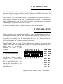
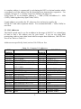
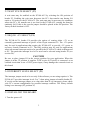
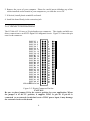
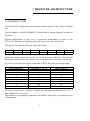
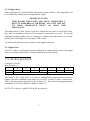
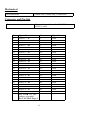
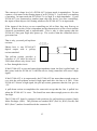
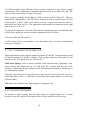
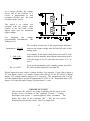
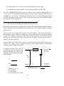
PC104-AC5 DIGITAL I/O User’s Manual Revision 1 October, 2000 Your new Measurement Computing product comes with a fantastic extra — Management committed to your satisfaction! Thank you for choosing a Measurement Computing product—and congratulations! You own the finest, and you can now enjoy the protection of the most comprehensive warranties and unmatched phone tech support. It’s the embodiment of our mission: To provide data acquisition hardware and software that will save time and save money. Simple installations minimize the time between setting up your system and actually making measurements. We offer quick and simple access to outstanding live FREE technical support to help integrate MCC products into a DAQ system. Limited Lifetime Warranty: Most MCC products are covered by a limited lifetime warranty against defects in materials or workmanship for the life of the product, to the original purchaser, unless otherwise noted. Any products found to be defective in material or workmanship will be repaired, replaced with same or similar device, or refunded at MCC’s discretion. For specific information, please refer to the terms and conditions of sale. Harsh Environment Program: Any Measurement Computing product that is damaged due to misuse, or any reason, may be eligible for replacement with the same or similar device for 50% of the current list price. I/O boards face some harsh environments, some harsher than the boards are designed to withstand. Contact MCC to determine your product’s eligibility for this program. 30 Day Money-Back Guarantee: Any Measurement Computing Corporation product may be returned within 30 days of purchase for a full refund of the price paid for the product being returned. If you are not satisfied, or chose the wrong product by mistake, you do not have to keep it. These warranties are in lieu of all other warranties, expressed or implied, including any implied warranty of merchantability or fitness for a particular application. The remedies provided herein are the buyer’s sole and exclusive remedies. Neither Measurement Computing Corporation, nor its employees shall be liable for any direct or indirect, special, incidental or consequential damage arising from the use of its products, even if Measurement Computing Corporation has been notified in advance of the possibility of such damages. Trademark and Copyright Information Measurement Computing Corporation, InstaCal, Universal Library, and the Measurement Computing logo are either trademarks or registered trademarks of Measurement Computing Corporation. Refer to the Copyrights & Trademarks section on mccdaq.com/legal for more information about Measurement Computing trademarks. Other product and company names mentioned herein are trademarks or trade names of their respective companies. © 20 Measurement Computing Corporation. All rights reserved. No part of this publication may be reproduced, stored in a retrieval system, or transmitted, in any form by any means, electronic, mechanical, by photocopying, recording, or otherwise without the prior written permission of Measurement Computing Corporation. Notice Measurement Computing Corporation does not authorize any Measurement Computing Corporation product for use in life support systems and/or devices without prior written consent from Measurement Computing Corporation. Life support devices/systems are devices or systems that, a) are intended for surgical implantation into the body, or b) support or sustain life and whose failure to perform can be reasonably expected to result in injury. Measurement Computing Corporation products are not designed with the components required, and are not subject to the testing required to ensure a level of reliability suitable for the treatment and diagnosis of people. +03&$&OZS Table of Contents 1 INTRODUCTION ................................. 1 2 INSTALLATION . . . . . . . . . . . . . . . . . . . . . . . . . . . . . . . . . . . . 1 2.1 BASE ADDRESS . . . . . . . . . . . . . . . . . . . . . . . . . . . . . . . . . 1 2.2 WAIT STATE SELECT (P3) . . . . . . . . . . . . . . . . . . . . . . . . 3 2.3 IRQ IN/ +5V SELECT (P4) . . . . . . . . . . . . . . . . . . . . . . . . . . 3 2.4 INTERRUPT LEVEL SELECT (P5) . . . . . . . . . . . . . . . . . . . 3 2.5 INSTALLING THE BOARD . . . . . . . . . . . . . . . . . . . . . . . . 3 2.6 CONNECTOR DIAGRAM . . . . . . . . . . . . . . . . . . . . . . . . . . 4 3 REGISTER ARCHITECTURE . . . . . . . . . . . . . . . . . . . . . . . . . 5 3.1 INTRODUCTION . . . . . . . . . . . . . . . . . . . . . . . . . . . . . . . . . 6 3.2 DIGITAL DATA REGISTERS . . . . . . . . . . . . . . . . . . . . . . . 7 3.3 CONTROL REGISTER . . . . . . . . . . . . . . . . . . . . . . . . . . . . . 8 4 SPECIFICATIONS . . . . . . . . . . . . . . . . . . . . . . . . . . . . . . . . . . 10 5 ELECTRONICS AND INTERFACING . . . . . . . . . . . . . . . . . 12 5.1 INTRODUCTION . . . . . . . . . . . . . . . . . . . . . . . . . . . . . . . . 12 5.2 PULL UP & PULL DOWN RESISTORS . . . . . . . . . . . . . . 12 5.3 TTL TO SOLID STATE RELAYS . . . . . . . . . . . . . . . . . . . 14 5.4 VOLTAGE DIVIDERS . . . . . . . . . . . . . . . . . . . . . . . . . . . . 14 5.5 LOW PASS FILTERS DE-BOUNCE INPUTS . . . . . . . . . . 16 This page is blank. 1 INTRODUCTION The PC104-AC5 is a 24-line digital I/O board. The control register which sets the direction of the I/O ports is identical to an 8255 in mode 0 (see 8255 data sheet). The I/O pins are high-drive TTL compatible. The connector is a 50-pin header which is compatible with the pin-out of OPTO-22 and GORDOS solid state relay racks. If you are using an OPTO or GORDOS form factor solid state relay rack, the PC104-AC5 can be connected directly to the relay rack through a 50-pin cable such as the C50FE-2. A group of application notes is included to assist in electrical interfacing. 2 INSTALLATION Before you open your computer and install the board, install and run InstaCal, the installation, calibration and test utility included with your board. InstaCal will guide you through switch and jumper settings for your board. Detailed information regarding these settings can be found below. Refer to the Extended Software Installation manual for InstaCal installation instructions. The PC104-AC5 has one bank of base address-select switches, an interrupt select jumper, a wait state select jumper and a jumper for configuring the function of pin 49 which must be set before installing the board in your computer. 9 8 7 6 5 4 3 22 Sw Hex A9 A8 A7 A6 A2 A5 A4 A3 A2 2.1 BASE ADDRESS On the base address switches, (Figure 2-1), each switch position corresponds to one of the PC bus address lines. By placing the switch down, the address decode logic responds to that address bit. 200 100 80 40 04 20 10 8 4 Figure 2-1. Base Address Switch - 300h Shown 1 A complete address is constructed by calculating the HEX or decimal number which corresponds to all the address bits the board has been instructed to respond to. For example, in Figure 2-1, switches 9 and 8 are DOWN, all others UP. Using figure 2-1 as an example, address 9 = 200h (512D) and address 8 = 100h (256D); added together they equal 300h (768D). Certain address are used by the PC, others are free and may be used by the PC104-AC5 and other expansion boards. We recommend BASE = 300h (768D) be tried first. 2.1.1 I/O Addresses The BASE switch may be set for an address in the range of 000-3FC so it should not be hard to find a free address area for your board. If you are not using IBM prototyping cards or some other board which occupies these addresses, 300-31Fh are free to use. Refer to Table 2-1. Addresses not specifically listed, such as 390-39Fh, are free. Table 2-1. Computer I/O Addresses HEX RANGE 000-00F 020-021 040-043 060-063 060-064 070-071 080-08F 0A0-0A1 0A0-0AF 0C0-0DF 0F0-0FF 1F0-1FF 200-20F 210-21F 238-23B 23C-23F 270-27F 2B0-2BF FUNCTION 8237 DMA #1 8259 PIC #1 8253 TIMER 82C55 PPI (XT) 8742 CONTROLLER (AT) CMOS RAM & NMI MASK (AT) CARD DMA PAGE REGISTERS 8259 PIC#2 NMI MASK (XT) 8237 #2 (AT) 80287 NUMERIC CO-P (AT) HARD DISK (AT) GAME CONTROL EXPANSION UNIT (XT) BUS MOUSE ALT BUS MOUSE PARALLEL PRINTER EGA 2 HEX RANGE 2C0-2CF 2D0-2CF 2E0-2E7 2E8-2EF 2F8-2FF 300-30F FUNCTION EGA EGA GPIB (AT) SERIAL PORT SERIAL PORT PROTOTYPE 310-31F 320-32F 378-37F 380-38F 3A0-3AF 3B0-3BB 3BC-3BF 3C0-3CF 3D0-3DF 3E8-3EF 3F0-3F7 3F8-3FF PROTOTYPE CARD HARD DISK (XT) PARALLEL PRINTER SDLC SDLC MDA PARALLEL PRINTER EGA CGA SERIAL PORT FLOPPY DISK SERIAL PORT 2.2 WAIT STATE SELECT (P3) A wait state may be enabled on the PC104-AC5 by selecting the ON position of header P3. Enabling the wait state decreases the PC’s bus transfer rate during I/O reads or I/O writes to the PC104-AC5. The wait state may be necessary for situations where the PC’s I/O transfer rate is too fast for the PC104-AC5, causing the board to randomly fail. If this is the case the jumper should be placed in the ON position. The factory default location is OFF. 2.3 IRQ IN/ +5V SELECT (P4) The PC104-AC5’s header P4 provides the option of routing either +5V or an externally generated interrupt to pin 49 of the 50-pin connector P1. The +5V option may be used in applications that require the PC104-AC5 to provide +5V power to accessory boards connected to P1. The IRQ position may be used for applications where an external interrupt needs to be passed to the PC104-AC5 which is then passed to PC. The particular interrupt level to be used can be selected using header P5 (see section 2.4). CAUTION Be sure to place jumper P4 in the correct position for your application. When the jumper is in the 5V position, it supplies 5VDC to pin 49. If pin 49 is connected to an external circuit that is not a 5VDC power input, it may damage the external circuit or this board. 2.4 INTERRUPT LEVEL SELECT (P5) The interrupt jumper needs to be set only if the software you are using requires it. The PC104-AC5 provides interrupt levels 2 to 7 when using jumper-selectable header P5. If you do set the interrupt jumper to a value other than X (no interrupt), please check your PC’s current configuration for possible interrupt conflicts. The factory default setting is no interrupt (P5, position X). 2.5 INSTALLING THE BOARD 1. Turn the power off. 3 2. Remove the cover of your computer. Please be careful not to dislodge any of the cables installed on the boards in your computer as you slide the cover off. 3. If desired, install plastic standoffs on board. 4. Install the board firmly in the extension jack. 2.6 CONNECTOR DIAGRAM The PC104-AC5 I/O uses a 50-pin header-type connector. The signals available are direct connections to an 82C55 digital I/O integrated circuit. Figure 2-2 shows the pin outs for the connector. PORT C7 1 PORT C6 3 PORT C5 5 PORT C4 7 PORT C3 9 PORT C2 11 PORT C1 13 PORT C0 15 PORT B7 17 PORT B6 19 PORT B5 21 PORT B4 23 PORT B3 25 PORT B2 27 PORT B1 29 PORT B0 31 PORT A7 33 PORT A6 35 PORT A5 37 PORT A4 39 PORT A3 41 PORT A2 43 PORT A1 45 PORT A0 47 IRQ IN OR 5VDC 49 2 4 6 8 10 12 14 16 18 20 22 24 26 28 30 32 34 36 38 40 42 44 46 48 50 Figure 2-2. Digital Connector Pin Out CAUTION Be sure to place jumper P4 in the correct position for your application. When the jumper is in the 5V position, it supplies 5VDC to pin 49. If pin 49 is connected to an external circuit that is not a 5VDC power input, it may damage the external circuit or this board. 4 This board is typically used for driving the SSR-PB24 solid state relay rack. For this application, the C50FE-# cable is used. If your application requires point to point wiring, you may want to consider the C50FF-# cable and a screw terminal board to simplify connections to the PC104-AC5. Please refer to the information on the CIO-TERM100, CIO-SPADE50 and CIO-MINI50 screw terminal boards or the SCB-50 and SCB-100 screw terminal boards and enclosure. 5 3 REGISTER ARCHITECTURE 3.1 INTRODUCTION The PC104-AC5 contains three data and one control register for the 24 lines of digital I/O. The first address, or BASE ADDRESS, is determined by setting a bank of switches on the board. Register manipulation is best left to experienced programmers as most of the PC104-AC5 functions are implemented in the easy to use Universal Library. The register descriptions follow all follow the format: 7 A7 6 A6 5 A5 4 A4 3 A3 2 A2 1 A1 0 A0 Where the numbers along the top row are the bit positions within the 8-bit byte and the numbers and symbols in the bottom row are the functions associated with that bit. To write to or read from a register in decimal or HEX, the following weights apply: BIT POSITION 0 1 2 3 4 5 6 7 DECIMAL VALUE 1 2 4 8 16 32 64 128 HEX VALUE 1 2 4 8 10 20 40 80 To write a control word or data to a register, the individual bits must be set to 0 or 1 then combined to form a byte. The method of programming required to set/read bits from bytes is beyond the scope of this manual. 6 In summary form, the registers and their function are listed on the following table. Within each register are eight bits which may constitute a byte of data or eight individual bit set/read functions. ADDRESS BASE +0 BASE +1 BASE +2 BASE +3 Table 3-1. Board Register Functions READ FUNCTION WRITE FUNCTION 1st Port A Input 1st Port A Output 1st Port B Input 1st Port B Output 1st Port C Input 1st Port C Output None. Configure I/O 3.2 DIGITAL DATA REGISTERS Port A Base Address + 0 7 6 A7 A6 5 A5 4 A4 3 A3 2 A2 1 A1 0 A0 Port B Data Base Address +1 7 6 B7 B6 5 B5 4 B4 3 B3 2 B2 1 B1 0 B0 Ports A & B may be programmed as input or output. Each is written to and read from in bytes, but for control and monitoring, use individual bits. When using bit set/reset and bit read functions, unwanted bits must be masked out of reads and ORed into writes. Port C Data Base Address +2 7 6 C7 C6 CH3 CH2 5 C5 CH1 4 C4 CH0 3 C3 CL3 2 C2 CL2 1 C1 CL1 0 C0 CL0 Port C may be used as one 8-bit port of either input or output, or it may be split into two 4-bit ports which may be independently input or output. The notation for the upper 4-bit port is CH3 - CH0, and for the lower, CL3 - CL0. Although it may be split, every read and write to port C carries eight bits of data so unwanted information must be ANDed out of reads, and writes must be ORed with the current status of the other port. 7 3.2.1 Output Ports Ports configured for output hold the output data written to them. This output byte can be read back by reading a port configured for output. IMPORTANT NOTE THIS BOARD EMULATES THE 82C55. WHENEVER A 82C55 IS POWERED ON OR RESET, ALL PINS ARE SET TO HIGH IMPEDANCE INPUT. SO DOES OUR EMULATION. The implications of this is that if you have output devices such as solid state relays, they may be switched on whenever the computer is powered on or reset. To prevent unwanted switching and to drive all outputs to a known state after power on or reset, pull all pins either high or low through a 10K resistor. To install pull up/down resistor packs, see the application note. 3.2.2 Input Ports In 82C55 mode 0 configuration, ports configured for input read the state of the input lines at the moment the read is executed, transitions are not latched. 3.3 CONTROL REGISTER Configure A, B & C Base Address +3 7 6 N/A N/A 5 4 N/A A Group A 3 CU 2 N/A 1 B Group B 0 CL The Ports A, B, C High and C Low may be independently programmed for input or output. The most commonly used mode for an 82C55 is mode 0, input / output mode. This is the only mode supported by the PC104-AC5. The codes for programming the emulated 82C55 in this mode are shown in Table 3-2. NOTE: D7 is always 1 and D6, D5 & D2 are always 0. 8 D4 0 0 0 0 0 0 0 0 1 1 1 1 1 1 1 1 Table 3-2. 82C55 Emulation Programming Codes - Mode 0 D3 D1 D0 HEX DEC A CU B 0 0 0 80 128 OUT OUT OUT 0 0 1 81 129 OUT OUT OUT 0 1 0 82 130 OUT OUT IN 0 1 1 83 131 OUT OUT IN 1 0 0 88 136 OUT IN OUT 1 0 1 89 137 OUT IN OUT 1 1 0 8A 138 OUT IN IN 1 1 1 8B 139 OUT IN IN 0 0 0 90 144 IN OUT OUT 0 0 1 91 145 IN OUT OUT 0 1 0 92 146 IN OUT IN 0 1 1 93 147 IN OUT IN 1 0 0 98 152 IN IN OUT 1 0 1 99 153 IN IN OUT 1 1 0 9A 154 IN IN IN 1 1 1 9B 155 IN IN IN 9 CL OUT IN OUT IN OUT IN OUT IN OUT IN OUT IN OUT IN OUT IN 4 SPECIFICATIONS Typical for 25°C unless otherwise specified. Power consumption +5V Operating PC104-AC5 625 mA typical, 960 mA max Digital Input / Output Digital type Number of I/O Configuration Input low voltage Input high voltage Output low voltage Output high voltage High Level Output Current Low Level Output Current Absolute maximum input voltage Pull-Up/Pull-Down Resistors Power On / Reset Digital Outputs - 74S244 Digital Inputs - 74LS373 24 2 banks of 8 bits each and 2 banks of 4 bits each (8255A mode 0 emulation) Each bank programmable as either input or output 0.8V max. 2.0V min. 0.5V max. (Iol = 64 mA) 2.4V min. (Ioh = −15 mA) −15 mA max. 64 mA max. +5.5V max. Locations provided for user-installation. High impedance Interrupts Interrupt Source Interrupt Levels Interrupt enable/disable External 2, 3, 4, 5, 6, 7 (jumper-selectable) Jumper-selectable (P4) Environmental Operating Temperature Range Storage Temperature Range Humidity 0 to 70°C −40 to 100°C 0 to 95% non-condensing 10 Mechanical Card dimensions 103mm wide x 96mm long x 15mm thick Connector and Pin Out Connector Pin 1 3 5 7 9 11 13 15 17 19 21 23 25 27 29 31 33 35 37 39 41 43 45 47 49 50-pin. Compatible with SSR-PB24 using C50FE-x cable Signal Name PORT C – B7 PORT C – B6 PORT C – B5 PORT C – B4 PORT C – B3 PORT C – B2 PORT C – B1 PORT C – B0 PORT B – B7 PORT B – B6 PORT B – B5 PORT B – B4 PORT B – B3 PORT B – B2 PORT B – B1 PORT B – B0 PORT A – B7 PORT A – B6 PORT A – B5 PORT A – B4 PORT A – B3 PORT A – B2 PORT A – B1 PORT A – B0 IRQ IN OR +5V Out (jumper-selectable) See CAUTION Page 4 Pin 2 4 6 8 10 12 14 16 18 20 22 24 26 28 20 32 34 36 38 40 42 44 46 48 50 11 Signal Name GND GND GND GND GND GND GND GND GND GND GND GND GND GND GND GND GND GND GND GND GND GND GND GND GND 5 ELECTRONICS AND INTERFACING 5.1 INTRODUCTION This short introduction to the electronics most often needed by digital I/O board users covers the following topics: y y y y y y y Pull up/pull down resistors Transistors Power MOSFETs Solid State Relays Voltage Dividers Low Pass Filters for digital inputs Noise; sources and solutions IMPORTANT NOTE This board emulates the 82C55. WHENEVER THE 82C55 IS POWERED ON OR RESET, ALL PINS ARE SET TO HIGH IMPEDANCE INPUT. The implications of this fact is that if you have output devices such as solid state relays, they may be switched on whenever the computer is powered on or reset. To prevent unwanted switching and to drive all outputs to a known state after power on or reset, pull all pins either high or low through a 2.2K resistor. To install pull up/down resistor packs, see the application note. 5.2 PULL UP & PULL DOWN RESISTORS This description deals with pull up/down resistors and the emulated 82C55 digital I/O. Whenever the PC104-AC5 is powered on or reset, the control register is set to a known state. That state is mode 0, all ports are inputs. When used as an output device to control other TTL input devices, the PC104-AC5 applies a voltage level of 0V for low and 2.5V to 5V for high. 12 The concept of voltage level of a PC104-AC5 in input mode is meaningless. Do not connect a volt meter to the floating input of an PC104-AC5. It will show you nothing of meaning. In input mode the PC104-AC5 is in 'high Z' or high impedance. If your PC104-AC5 was connected to another input chip (the device you were controlling), the inputs of that chip are left floating whenever the PC104-AC5 is in input mode. If the inputs of the device you are controlling are left to float, they may float up or down. Which way they float is dependent on the characteristics of the circuit and the electrical environment; and is unpredictable This is why it often appears that the PC104-AC5 has gone 'high' after power up. The result is that the controlled device gets turned on. That is why you need pull up/down resistors. 8 2 C 5 5 E m u la t e d C ir c u it Shown here is one PC104-AC5 digital output with a pull-up resistor attached. The pull-up resistor provides a reference to +5V while its value of 2200 ohms allows only about 2 mA to flow through the circuit. If the PC104-AC5 is reset and enters high impedance input, the line is pulled high. At that point, both the PC104-AC5 AND the device being controlled will sense a high signal. If the PC104-AC5 is in output mode, the PC104-AC5 has more than enough power to over ride the pull-up/down resistor's high signal and drive the line to 0 volts. If the PC104-AC5 asserts a high signal, the pull up resistor guarantees that the line goes to +5V. A pull-down resistor accomplishes the same task except that the line is pulled low when the PC104-AC5 is reset. The board has more than enough power to drive the line high. The PC104-AC5 board is equipped with positions for pull-up/down resistors Single Inline Packages (SIPs). The positions are marked RN1 (Port A), RN2 (Port B) and RN3 (Port C) and are located beside the connector P1. 13 A 2.2Kohm, eight-resistor SIP has all its resistors connected on one end to a single common pin. The common pin is marked with a dot and is at one end of the SIP. The other resistor ends connect to eight in-line pins. There are three locations for installation of SIP resistors on the PC104-AC5. They are marked RN1 through RN3. The SIP can be installed to pull-up or pull-down. At each location, RN1, 2, and 3, there are 10 holes in a line. On one end of the line a hole is marked HI; the other end LO. The eight holes in the middle are connected to the eight lines of a port, A, B, or C. To pull-up all eight lines, orient the SIP with the common pin (dot) in the HI hole end; to pull-down, install the resistor with the common pin in the LO hole. Carefully solder the SIP in place. A 2.2K resistor SIP is recommended. Use other values only if you have calculated the necessity of doing so. 5.3 TTL TO SOLID STATE RELAYS Many applications require digital outputs to switch AC and DC voltage motors on and off and to monitor AC and DC voltages. High voltages cannot be controlled or read directly by the TTL digital lines of a PC104-AC5. Solid State Relays, such as those available from Measurement Computing Corp. allow control and monitoring of AC and high DC voltages and provide 750V isolation. Solid State Relays (SSRs) are the recommended method of interfacing to AC and high DC signals. The most convenient way to use solid state relays and a PC104-AC5 board is to use a Solid State Relay Rack. A SSR Rack circuit board has output buffers to switch the socketed SSRs. SSR Racks are available from Measurement Computing Corp. 5.4 VOLTAGE DIVIDERS To measure a signal greater than the input range of a digital input, use a voltage divider to drop the voltage of the input to the level the board can safely accept. 14 In a voltage divider, the voltage across one of the resistors in a circuit is proportional to that resistance divided into the total resistance in the circuit. The object is to choose two resistors with the proper ratio relative to the full scale of the digital input and the maximum signal voltage. For dropping the voltage proportionally (attenuation) the formula for is: Attenuation = R1+R2 R2 2 = 10K+10K 10K R1=(A-1)*R2 The variable Attenuation is the proportional difference between the signal voltage max and the full scale of the analog input. For example, if the signal varies between 0 and 20 volts and you wish to measure that with an analog input with a full scale range of 0 to 10 volts, the Attenuation is 2:1 or just 2. For a given attentuation, pick a handy resistor and call it R2, then use this formula to calculate R1. Digital inputs also may require voltage dividers. For example, if you wish to input a 24 volt digital signal, you cannot connect that directly to the PC104-AC5 digital inputs. The voltage must be dropped to 5 volts max. The Attenuation is 24:5 or 4.8. Use the equation above to find an appropriate R1 if R2 is 1K. Remember that a TTL input is 'on' when the input voltage is greater than 2.5 volts. IMPORTANT NOTE The resistors, R1 and R2, are going to dissipate all the power in the divider circuit according to the equation Current = Voltage / Resistance and power = current-squared times resistance. The higher the value of the resistance (R1 + R2) the less power dissipated by the divider circuit. Here is a simple rule: 15 For Attenuation of 5:1 or less, no resistor should be less than 10K. For Attenuation of greater than 5:1, no resistor should be less than 1K. The CIO-TERMINAL has the circuitry on board to create custom voltage dividers. It is a 16" by 4" screw terminal board with two 37-pin, D-type connectors and 56 screw terminals (12 - 22 AWG). Designed for table top, wall, or rack mounting, the board provides prototype, divider circuit, filter circuit and pull-up resistor positions which you can use for your application. 5.5 LOW PASS FILTERS DE-BOUNCE INPUTS A low-pass filter between a signal source and an A/D board attenuates higher than the cut-off frequency, preventing them from entering the A/D board's analog or digital input circuits. The key term in a low pass filter circuit is cut-off frequency. The cut-off frequency is that frequency above which no variation of voltage with respect to time may enter the circuit. For example, if a low pass filter had a cut-off frequency of 30 Hz, the kind of interference associated with line voltage (60 Hz) would be largely filtered out but a signal of 25 Hz would pass. Low-pass filters are often used to remove a switch-bounce noise signal from a switch closure. The signal can be complex and have quite high frequency components requiring a more sophisticated filter. A simple low-pass filter can be constructed from one resistor (R) and one capacitor (C). The cut off frequency is determined according to the formula: Signal High A/D Board High Input R C Signal Volts Fc = 1 2*Pi*R*C R= 1 2*Pi*C*Fc Signal Low LOW PASS FILTER - Fc = Where Pi = 3.14... R is in Ohms C is in Farads Fc is in cycles per second. 16 A/D Board Low Input 1 2*Pi*R*C For your notes. 17 For your notes. 18 EC Declaration of Conformity We, Measurement Computing Corp., declare under sole responsibility, that the product: PC104-AC5 Part Number Digital I/O Board Description to which this declaration relates, meets the essential requirements, is in conformity with, and CE marking has been applied according to the relevant EC Directives listed below using the relevant section of the following EC standards and other normative documents: EU EMC Directive 89/336/EEC: Essential requirements relating to electromagnetic compatibility. EU 55022 Class B: Limits and methods of measurements of radio interference characteristics of information technology equipment. EN 50082-1: EC generic immunity requirements. IEC 801-2: Electrostatic discharge requirements for industrial process measurement and control equipment. IEC 801-3: Radiated electromagnetic field requirements for industrial process measurements and control equipment. IEC 801-4: Electrically fast transients for industrial process measurement and control equipment. Carl Haapaoja, Director of Quality Assurance Measurement Computing Corporation 10 Commerce Way Suite 1008 Norton, Massachusetts 02766 (508) 946-5100 Fax: (508) 946-9500 E-mail: [email protected] www.mccdaq.com