1
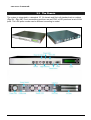
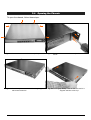
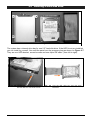
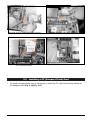
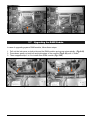
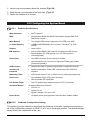
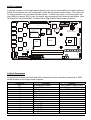
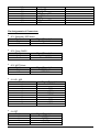
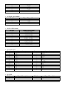
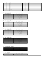
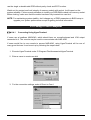
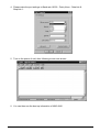
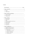
NAR-4040
Communications Appliance
User′s Manual
Revision: 010
Portwell Inc.
3F, No. 92, Nei-Hu Rd., Sec. 1, Taipei 114, Taiwan, R.O.C.
Headquarter: +886-2-2799-2020
Fax: +886-2-2799-1010
http://www.portwell.com.tw
Email: [email protected]
ITEM NO: B8980650
Table of Contents
Chapter 1
Introduction
1.1
About This Manual .....................................................................................3
1.2
Manual Organization ..................................................................................3
1.3
Text Conventions .......................................................................................4
Chapter 2
Getting Started
2.1
Included Hardware .....................................................................................5
2.2
Before You Begin .......................................................................................5
2.3
The Chassis ..............................................................................................6
2.4
Opening the Chassis ..................................................................................7
2.5
Installing a Hard Disk Drive ........................................................................8
2.6
Installing a CF (Compact Flash) Card ........................................................9
2.7
Upgrading the RAM Module .....................................................................10
2.8
Replace the Battery ..................................................................................11
2.9
Installing a Different Processor .................................................................11
2.10
PCI Card Install & Remove ......................................................................13
2.11
Assembling the System ............................................................................14
2.12
Configuring the System Board .................................................................15
2.13
Installing Memory ......................................................................................20
2.14
Using a Client Computer ..........................................................................21
Chapter 3
3.1
Operation Guides
5
24
Brief Guide for PPAP-3711VL ..................................................................24
Chapter 4
Appendix
4.1
GPIO Sample code ..................................................................................27
4.2
Watch-Dog Timer Sample code ...............................................................31
4.3
Reset To Default Sample code ................................................................33
Chapter 5
5.1
3
EZIO-100
27
46
About EZIO-100 ..........................................................................................46
5.2
Features
5.3
Mechanical Specification ..........................................................................46
5.4
General Specification ...............................................................................47
5.5
Product Outlook........................................................................................47
5.6
Interface Pin Assignment .........................................................................47
5.7
EZIO Function Command.........................................................................48
5.8
Character Generator ROM (CGROM) ......................................................52
NAR-4040 User’s Manual
............................................................................................46
1
5.9
Sample Code............................................................................................53
NAR-4040 User’s Manual
2
Chapter 1
Introduction
1.1 About This Manual
This manual describes all required information for setting up and using the NAR-4040.
NAR-4040 provides the essential components for delivering optimal performance and
functionality in the value communications appliance market segment. This manual should help
its users to get familiar with NAR-4040 to be able to fulfill requirements.
Feature of NAR-4040 includes:
◆ Versatile networking and I/O capabilities: 4 Ethernet ports
◆ Foul USB ports
◆
Two COM ports
◆
One VGA Port
◆
One CF Card Socket
◆
One EZIO Display
◆ Up to 2G byte of DDR memory
◆ Two on-board DMA100 IDE channel to support two IDE hard disk drives
◆ CE NO:
◆ FCC NO:
1.2 Manual Organization
The manual describes how to configure your NAR-4040 system to meet various operating
requirements. It is divided into three chapters, with each chapter addressing a basic concept
and operation of this whole system.
Chapter 1: Introduction. It briefly talks about how this documentation is about. Some guidelines
for users who do not want to read through all the pages, but still finding what they
need.
Chapter 2: Hardware Configuration Setting and Installation. This chapter shows how the
hardware was put together. Detail information is also included in this section of this
article. It shows the definitions and locations of Jumpers and Connectors that you
can easily configure your system. Descriptions on how to properly mount the CPU
and main memory to get a safe installation. By reading this chapter, the users should
be able to set up NAR-4040.
Chapter 3: Operation Information. It illustrates the main board system architecture. This section
intends to give the users more information on the system architecture and how its
performance can be maximized.
Any updates to this manual, technical clarification, and answers to frequently asked questions
will be posted on the following web site: http://isc.portwell.com.tw
NAR-4040 User’s Manual
3
1.3 Text Conventions
Users may find helpful tips or related information on Portwell's Web site.
http://www.portwell.com.tw. A direct contact to Portwell's technical person is also available.
For further support Users may also contact our headquarter in Taipei or contact Portwell's
distributors.
NAR-4040 User’s Manual
4
Chapter 2
Getting Started
This section describes how the hardware installation and system settings should be done.
2.1 Included Hardware
The following hardware is included in your kit:
◆
◆
◆
◆
◆
◆
◆
PPAP-3711VL Net Appliance System board
250 W power supply
1U Chassis
One serial port cable
One VGA cable
One USB cable
One EZIO
2.2 Before You Begin
To prevent damage to any system board, it is important to handle it with care. The following
measures are generally sufficient to protect your equipment from static electricity discharge:
When handling the board, use a grounded wrist strap designed for static discharge elimination.
Touch a grounded metal object before removing the board from the antistatic bag. Handle the
board by its edges only; do not touch its components, peripheral chips, memory modules or gold
contacts.
When handling processor chips or memory modules, avoid touching their pins or gold edge
fingers. Put the value communications appliance system board and peripherals back into the
antistatic bag when they are not in use or not installed in the chassis.
Some circuitry on the system board can continue to operate even though the power is switched
off. Under no circumstances should the Lithium coin cell that is being used to power the realtime clock be allowed to be shorted. The coin cell can heat under these conditions and present
a burn hazard.
WARNING
1.
“CAUTION: DANGER OF EXPLOSION IF BATTERY IS INCORRECTLY REPLACED.
REPLACE ONLY WITH SAME OR EQUIVALENT TYPE RECOMMENDED BY THE
MANTFATURER. DISCARD USED BATTERIES ACCORDING TO THE
MANUFACTURER’S INSTRUCTIONS ”
2.
This guide is for technically qualified personnel who have experience installing and
configuring system boards Disconnect the system board power supply from its
power source before you connect or disconnect cables or install or remove any
system board components. Failure to do this can result in personnel injury or
equipment damage.
3.
Avoid short-circuiting the lithium battery; this can cause it to superheat and cause
burns if touched.
4.
Do not operate the processor without a thermal solution. Damage to the processor
NAR-4040 User’s Manual
5
can occur in seconds.
2.3 The Chassis
The system is integrated in a standard 19" 1U chassis and fits in all standard rack or cabinet
(Fig. 2-1 , Fig. 2-2). Front accessible panel there are an EZIO, a LED panel and a set of LAN
ports. The LAN ports number can be different according to model.
Fig. 2-1 Front View of the Chassis
NAR-4040 User’s Manual
Fig. 2-2 Rear View of the Chassis
6
2.4 Opening the Chassis
To open the chassis, follow these steps:
Fig. 2-3 Remove the screw on the arrow tip of top-cover
Fig. 2-5 Push the top-cover on both left and right upper
side at the same time
NAR-4040 User’s Manual
Fig. 2-4 Remove the screw on the arrow tip of the ear
mount
Fig. 2-6 Slide lightly the top-cover to rear side until it is
stopped and then raise it up
7
2.5 Installing a Hard Disk Drive
Fig. 2-7
The system has a internal drive bay for one 2.5" hard disk drive. If the HDD is not pre-installed,
you can install by yourself. You need the parts from the accessory-bag as shown on Figure 2-7.
They are one HDD-bracket, several screws and one 44pin IDE cable. (from left to right).
Fig. 2-8 Fix the hard disk drive on the HDD
bracket with four sink-head screws
NAR-4040 User’s Manual
Fig. 2-9
Plug the IDE cable into hard disk drive
connector
8
Fig. 2-10 Plug the 44-pin end to IDE connector
Fig. 2-12 Fix the half assembled HDD with the
four round head screws
Fig. 2-11 Bend the cable below the bracket
Fig. 2-13 Complete.
2.6 Installing a CF (Compact Flash) Card
1. To install a compact flash card, it needs only to insert the CF card into the white socket on
the adaptor board (Fig. 2-14)(Fig. 2-15)
NAR-4040 User’s Manual
9
Fig. 2-14
Fig. 2-15
2.7 Upgrading the RAM Module
In case of upgrading system RAM module, follow these steps:
1. Pull out the lock arms on both side and the RAM module springs up automatically. (Fig.2-22)
2. Press down gently on both left and right edges of the module (Fig.2-23) until it "clicks".
3. Then reappear step 1 to 2 to install more RAM module.(Fig. 2-25)
Fig. 2-22
NAR-4040 User’s Manual
Fig. 2-23
10
Fig. 2-22
Fig. 2-23
2.8 Replace the Battery
In case of replacing the battery, follow these steps:
Fig. 2-24
Fig. 2-25
1. Press the metal hook backward. (Fig.2-24)
2. The battery springs automatically. (Fig.2-25)
4. Replace a new one and press it back with fingertip.
2.9 Installing a Different Processor
Installing CPU
1. Lift the handling lever of CPU socket outwards and upwards to the other end.
2. Align the processor pins with holes on the socket. Make sure that the notched corner or
NAR-4040 User’s Manual
11
dot mark (pin 1) of the CPU corresponds to the socket's bevel end. Then press the CPU
gently until it fits into place. If this operation is not easy or smooth, don't do it forcibly. You
need to check and rebuild the CPU pin uniformly.
3. Push down the lever to lock processor chip into the socket.
4. Follow the installation guide of cooling fan or heat sink to mount it on CPU surface and
lock it on the socket 478.
5. Be sure to follow particular CPU speed and voltage type to adjust the jumper settings
properly.
Removing CPU
1. Unlock the cooling fan first.
2. Lift the lever of CPU socket outwards and upwards to the other end.
3. Carefully lift up the existing CPU to remove it from the socket.
4. Follow the steps of installing a CPU to change to another one or place handling bar to
close the opened socket.
2.11.1
Configuring Processor Speed
The system was designed to self-detect its CPU speed. So it does not require any system
adjustment.
Fig. 2-26 Lift the handling lever of CPU socket
outwards and upwards to the other end.
NAR-4040 User’s Manual
Fig. 2-27 insert CPU into theSocket
12
Fig. 2-28 Set the CPU to the position and drive
the screws
Fig. 2-29 insert the air dock and buckle up to
the system board as shown with red
arrow
Fig. 2-30 assembling completion diagram
2.10 PCI Card Install & Remove
If the installation of PCI cards required, please follow the instructions with care.
Fig. 2-31 PCI Card secure base
NAR-4040 User’s Manual
Fig. 2-32 Install the secure base to the chassis
13
Fig. 2-33 tight up the screws
Fig. 2-34 insert the PCI card into the PCI slot
Fig. 2-35 tight up the mooting screw of the PCI
card
2.11 Assembling the System
The mechanism of top cover assembly to chassis needs six screws to fix the top cover.
However, by assembling the top cover, there is one importance point; the tongue of the cover
must be inserted to the proper position, so the six screw holes on the cover can match to the
chassis.
Fig. 2-36
NAR-4040 User’s Manual
Fig. 2-37
14
1. Lay the top cover properly above the chassis (Fig.2-36)
2. Push the top cover towards to the front side. (Fig.2-37)
3. Fasten the chassis of all screws.
2.12 Configuring the System Board
2.12.1
Product Specifications
Main processor
•
Intel® Celeron™
BIOS
•
Award system BIOS with 64Kb Flash ROM to support DMI, PnP,
Redirect to console.
Main Memory
•
Two 184-pin DDR socket, supporting 2.5V DDR up to 2GB
L2 Cache Memory
•
128KB/512KB PBSRAM built in (Celeron™/Pentium® 4) CPU
module
Chipset
•
Intel® 845GV
IDE Interface
•
One on-board DMA33 IDE channel to support two IDE devices
Default support 2.5" IDE devices only (3.5" IDE requires a
converting cable)
Serial Ports
•
One DB9 Connector for connecting to console
•
One internal Pin pair connector for optional LCD/Key pad module
(Portwell Proprietary)
USB Interface
•
Support two USB 2.0 ports for high speed I/O peripheral devices
Auxiliary I/O
Interfaces
•
System reset switch, Power LED, LAN activity LED, HDD LED
interface
Watchdog Timer
•
255 intervals from 0.5 min. to 254.5 min. by software programming
Power Inlet
•
One standard 20-pin ATX power connector
•
One on-board DC input jack
PCI Golden Finger
•
One PCI golden finger edge connector for PCI connection
Hardware Monitor
On-board hardware monitor for:
• CPU fan x 1
• System fan x 2
• System voltages: +5V and +12V
Power Good
•
2.12.2
On-board power good generator with reset time, 300ms~500ms
Hardware Configuration Setting
This section gives the definitions and shows the positions of jumpers, headers and connectors.
All of the configuration jumpers on PPAP-3711VL are in the proper position. The default settings
set by factory are marked with a star ( ★ ).
NAR-4040 User’s Manual
15
2.12.2.1 Jumpers
In general, jumpers on the single board computer are used to select options for certain features.
Some of the jumpers are user-configurable, which allows system enhancement. The others are
for testing purpose only and should not be altered. To select any option, cover the jumper cap
over (Short) or remove (NC) it from the jumper pins according to the following instructions. Here
NC stands for "Not Connected". (Please refer to Fig. 2-38 for detail jumper positions)
LAN6
J15
J9
J2 J3
J7
J10
JP1
SIO
2
LAN4
2
2
2
4
4
4
J25
9
10
20
19
2
J19
BAT
J16
J24
J5
J8
13
26
FWH
LAN5
J4
5
10
5
10
J6
J11 J12 J13 J14
J20 J21 J22 J17 J18
J23
10
7
J26
mPGA478B
LAN3
845GV/GL
J27
ICH4
LAN2
J28
JP2
LAN1
J29
JP3 J30
J34
10 5
J31
J40
6
2
PW1
9
10
J33
DIMM1
DIMM2
2
4
J35
J39
J38
40
39
44
43
J32
J36
J37
Fig.2-38 PPAP-3711VL Jumper Locations
2.12.2.2 Connectors
I/O peripheral devices and Flash disk will be connected to these interface connectors or DOC
socket located on this single board computer.
Connector
JP1
JP2
JP3
J2
J3
J4
J5
J7
J8
J11
J12
J13
J14
J17
NAR-4040 User’s Manual
Function
Secondary IDE Select
Clean CMOS
WDT Select
K/B, M/S
CRT
Small 4 pin header
USB
Parallel port
GPIO
LAN6_LED
LAN5_LED
LAN4_LED
LAN3_LED
Load_Default
Remark
Shot: Master / Open: Slave
1-2: Normal , 2-3: Clean
Shot: WDT Reset / Open: SMI
16
J18
J20
J21
J22
J30
J31
J33
J34
Reset
LAN2_LED
LAN1_LED
HDD_PowerLED
Load_Default
COM2
HDD_PowerLED
USB
Pin Assignments of Connectors
●
●
●
●
●
JP1: Secondary IDE Select
Pin No.
Shot
NC
Signal Description
Master
Slave
JP2: Clean CMOS
Pin No.
1–2
2–3
Signal Description
Normal
Clean CMOS
JP3: WDT Select
Pin No.
Shot
NC
Signal Description
WDT Reset
WDT SMI
J2: K/B , M/S
Pin No.
1
2
3
4
5
6
7
8
9
10
J3: CRT
Pin No.
1
2
3
4
NAR-4040 User’s Manual
Signal Description
MDAT
GND
VCC
MCLK
KDAT
GND
VCC
KCLK
Signal Description
RED
GREEN
BLUE
VSYNCR
17
5
6
7
8
9
10
●
●
●
●
HSYNCR
DDCCL
GND
DDCDA
GND
J4: Small 4 pin header
Pin No.
1
2
3
4
Signal Description
+12V
GND
GND
VCC
J5/J34: USB Header
Pin No.
1
2
3
4
5
6
7
8
9
10
Signal Description
VCC2/VCC4
GND3/GND5
DATA2/DATA4
GND3/GND5
DATA2+/DATA4+
DATA3+/DATA5+
GND2/GND4
DATA3-/DATA5GND2/GND4
VCC3/VCC5
J7: Parallel port
Pin No.
Signal Description
1
P_STB#
3
P_PD1
5
P_PD3
7
P_PD5
9
P_PD7
11
BUSY
13
SLCT
15
ERR#
17
P_SLIN#
19
GND
21
GND
23
GND
25
GND
Pin No.
2
4
6
8
10
12
14
16
18
20
22
24
26
Signal Description
P_PD0
P_PD2
P_PD4
P_PD6
ACK#
PE
P_AFD#
P_INIT#
GND
GND
GND
GND
N/A
J8: GPIO
Pin No.
1
3
Pin No.
2
4
Signal Description
Signal Description
VCC
Di8
NAR-4040 User’s Manual
Do8
18
5
7
9
11
13
15
17
19
●
●
●
●
●
●
Di7
Di6
Di5
Di4
Di3
Di2
Di1
GND
6
8
10
12
14
16
18
20
J11: LAN6_LED
Pin No.
1
2
3
4
Signal Description
L6_1000#
L6_LINK LED#
L6_100#
L6_ACT
J12 : LAN5_LED
Pin No.
1
2
3
4
Signal Description
L5_1000#
L5_LINK LED#
L5_100#
L5_ACT#
J13 : LAN4_LED
Pin No.
1
2
3
4
Signal Description
L4_1000#
L4_LINK LED#
L4_100#
L4_ACT#
J14 : LAN3_LED
Pin No.
1
2
3
4
Signal Description
L3_1000#
L3_LINK LED#
L3_100#
L3_ACT#
J17/J30: Load_Default
Pin No.
1
2
Signal Description
PRE#
GND
J18 : RESET
Pin No.
Signal Description
NAR-4040 User’s Manual
Do7
Do6
Do5
Do4
Do3
Do2
Do1
GND
19
●
●
●
●
1
2
GND
RESET
J20 : LAN2_LED
Pin No.
1
2
3
4
Signal Description
L2_1000#
L2_LINK LED#
L2_100#
L2_ACT#
J21 : LAN5_LED
Pin No.
1
2
3
4
Signal Description
L1_1000#
L1_LINK LED#
L1_100#
L1_ACT#
J22/J33: HDD_Power LED
Pin No.
1
2
3
4
Signal Description
GND
VCC
HDD_ACT
VCC
J31: COM2
Pin No.
1
2
3
4
5
6
7
8
9
10
Signal Description
DCD#2
RXD#2
TXD#2
DTR#2
GND
DSR#2
RTS#2
CTS#2
RI#2
2.13 Installing Memory
This PPAP-3711VL provides one 184-pin DDR socket. The maximum memory size is 2GB.
Normally, the DDR used could be 2.5V DDR with speed less than 70ns (-7), you need to use
DDR with speed less than 70ns (-7). It is better to use PC2700-compliant memory chip on your
system.
For system compatibility and stability, don't use memory module without brand. You can also
NAR-4040 User’s Manual
20
use the single or double-side DDR without parity check and ECC function.
Watch out the contact and lock integrity of memory module with socket, it will impact on the
system reliability. Follow normal procedure to install your DDR RAM module into memory socket.
Before locking, make sure that the module has been fully inserted into card slot.
NOTE: For maintaining system stability, don't change any of DDR parameters in BIOS setup to
upgrade your system performance except for getting technical information.
2.14 Using a Client Computer
2.14.1
Connecting Using HyperTerminal
If users use a headless NAR-4040, which should have no mouse/keyboard and VGA output
connected to it. The console may be used to communicate with NAR-4040
If users would like to use console to access NAR-4040, using HyperTerminal will be one of
many good choices. It can be set up by following the steps below:
1. Execute HyperTerminal under C:\Program Files\Accessories\HyperTerminal
2. Enter a name to create new dial
3. For the connection settings, make it Direct to Com1.
NAR-4040 User’s Manual
21
4. Please make the port settings to Baud rate 19200,Parity None,Data bits 8,
Stop bits 1.
5. Turn on the power of raid, after following screen was shown
6. You can then see the boot up information of NAR-4040
NAR-4040 User’s Manual
22
7. This is the end of this section. If the terminal did not port correctly, please check the
previous steps.
NAR-4040 User’s Manual
23
Chapter 3
Operation Guides
3.1 Brief Guide for PPAP-3711VL
The PPAP-3711VL all-in-one half-sized network appliance system board is designed to fit a high
performance Celeron™ and Pentium® 4 based processor and compatible for high-end computer
system application. It is made to meet today's demanding pace, and keep complete compatibility
with hardware and software designed for the IBM PC/AT. It's beneficial to build up a high
performance and high data availability system for VARs, or system integrators.
This single board computer can run with Intel® FC-PGA Celeron™ or Intel® FC-PGA Pentium® 4
processors (Speed up to 2.8GHz), and 184-pin DDR up to 2GB. The enhanced on-board PCI
IDE interface support 2 drives up to PIO mode 4 timing and Ultra DMA/100 synchronous mode
feature. The on-board Super I/O Chipset integrates only two serial ports, which are driven by
two high performance 16C550-compatible UARTs to provide 16-byte send/receive FIFOs.
Besides, the two Universal Serial Bus ports provide high-speed data communication between
peripherals and PC.
The A built-in Watch-dog Timer function helps to monitor your system status. The on-board
Flash ROM is used to make the BIOS update easier. An AC/DC adaptor power input jack is
provided for AT mode operation. The high precision Real Time Clock/calendar is built to support
Y2K for accurate scheduling and storing configuration information. All of these features make
PPAP-3711VL excellent in stand-alone applications.
Fig. 3-1
System Architecture
The following illustration of block diagram will show how PPAP-3711VL be a highly integrated
system solution. The most up-to-date system architecture of PPAP-3711VL, includes two main
VLSI chips, 845GL/GV Host Bridge and 82810DB, to support FC-PGA Celeron/P4 processor,
DDR, PCI bus interface, USB 2.0 port, SMBus communication, and Ultra DMA/100 IDE Master.
The on-board super I/O chip, W83627HF, supports two UARTs.
NAR-4040 User’s Manual
24
PPAP-3711VL built-in Socket 478 to support Intel® FC-PGA Celeron™/Pentium® 4 processor
(both for 400/533 FSB bus only) for high performance and cost-effective application. The Intel®
Celeron™ processor is the next addition to the P6 micro architecture processor product lines.
The Intel® Celeron™ processor, like the Intel Pentium Pro and Intel Pentium II processor,
features a Dynamic Execution micro-architecture and also executes MMX technology
instructions for enhanced media and communication performance. However, the FC-PGA
Pentium® 4 processor provides 512K L2 Cache.
The North Bridge 845GL/GV provides a completely integrated solution for the system controller
and data path components in a Celeron™ processor system. It provides a 64-bit GTL+ based
host bus interface, optimized 64-bit DRAM interface without ECC to support two 2.5V DDR
memory module at the maximum bus frequency of 533 MHz, and 32-bit PCI bus interface to
support on-board PCI device.
The South Bridge, 82810DB, provides one channel dedicated Ultra DMA-100 IDE master/slave
interface, full Plug-and-Play compatibility, and one channel CF slot, Advanced Programmable
Interrupt Controller (APIC) interface on PPAP-3711VL. It also supports 4-port Universal Serial
Bus (USB 2.0) and PCI 2.1 Compliance operation.
The Super I/O chip W83627HF integrates two high-speed serial ports.In PPAP-3711VL, it
contains Watch-dog Timer (WDT) enabled by Software(BIOS). and Eight bit GPIO, Besides, an
advanced feature is used on PPAP-3711VL to support detection of CPU temperature.
Provides 64Kbit nVRAM(non-volatile RAM), and One 2x5 pin connector for VGA supported.
All detailed operating relations are shown in Fig. 3-2 PPAP-3711VL System Block Diagram.
NAR-4040 User’s Manual
25
Fig.3-2 PPAP-3711VL System Block Diagram
NAR-4040 User’s Manual
26
Chapter 4
Appendix
4.1 GPIO Sample code
/*
* led.c:
*
* Copyright (C) 2001 DeanSoft Co.,Ltd
* Copyright (C) 1998,2000,2001 Alessandro Rubini
*
* This program is free software; you can redistribute it and/or modify
* it under the terms of the GNU General Public License as published by
* the Free Software Foundation; either version 2 of the License, or
* (at your option) any later version.
*
* This program is distributed in the hope that it will be useful,
* but WITHOUT ANY WARRANTY; without even the implied warranty of
* MERCHANTABILITY or FITNESS FOR A PARTICULAR PURPOSE. See the
* GNU General Public License for more details.
*
* You should have received a copy of the GNU General Public License
* along with this program; if not, write to the Free Software
* Foundation, Inc., 59 Temple Place, Suite 330, Boston, MA 02111-1307, USA.
*/
#include <stdio.h>
#include <stdlib.h>
#include <string.h>
#include <unistd.h>
#include <errno.h>
#include <fcntl.h>
#include <sys/types.h>
#include <sys/stat.h>
#include <asm/io.h> /* linux-specific */
#ifdef __GLIBC__
# include <sys/perm.h>
#endif
// #define DEBUG
static unsigned int pmbase=0;
unsigned int read_port(unsigned int port,int size)
{
static int iopldone = 0;
unsigned int val=0;
NAR-4040 User’s Manual
27
if (port > 1024) {
if (!iopldone && iopl(3)) {
fprintf(stderr, " iopl(): %s\n", strerror(errno));
return 0;
}
iopldone++;
} else if (ioperm(port,size,1)) {
fprintf(stderr, " ioperm(%x): %s\n", port, strerror(errno));
return 0;
}
if (size == 4) {
val=inl(port);
#ifdef DEBUG
printf("Read_port:(0x%04x)=>0x%08x\n", port, val);
#endif
} else if (size == 2) {
val=inw(port);
#ifdef DEBUG
printf("Read_port:(0x%04x)=>0x%04x\n", port, val);
#endif
} else {
val=inb(port);
#ifdef DEBUG
printf("Read_port:(0x%04x)=>0x%02x\n", port, val);
#endif
}
return(val);
}
static int write_port(unsigned int port, unsigned int val, int size)
{
static int iopldone = 0;
#ifdef DEBUG
printf("Write_Port(0x%04x)<=0x%x\n", port, val);
#endif
if (port > 1024) {
if (!iopldone && iopl(3)) {
fprintf(stderr, "iopl(): %s\n", strerror(errno));
return 1;
}
iopldone++;
} else if (ioperm(port,size,1)) {
fprintf(stderr, "ioperm(%x): %s\n", port, strerror(errno));
return 1;
}
if (size == 4)
outl(val, port);
else if (size == 2)
NAR-4040 User’s Manual
28
outw(val&0xffff, port);
else
outb(val&0xff, port);
return 0;
}
void led_init()
{
unsigned int rval=0,mval=0;
// program bit 31,30,29 of PCR GENCFG to 1,1,1
write_port(0xCF8,0x800038B0,4);
rval=read_port(0xCFC,4);
mval=rval | 0xe0000000;
write_port(0xCF8,0x800038B0,4);
write_port(0xCFC,mval,4);
// program bit 8 of PCR XBCS to 0
write_port(0xCF8,0x8000384C,4);
rval=read_port(0xCFC,4);
mval=rval & 0xfffffeff;
write_port(0xCF8,0x8000384C,4);
write_port(0xCFC,mval,4);
// raed Power Management base address
write_port(0xCF8,0x80003B40,4);
rval=read_port(0xCFC,4);
pmbase=rval&0xFFC0;
}
//
// pos= 1~8 ,flag=1/0
//
void led_onoff(int pos, int flag)
{
unsigned int led=0;
switch (pos) {
case 1: // (D9) Bit5: 0-> led ON, 1-> led OFF
led = read_port(pmbase+0x37,1);
led=( flag==1 ?(led & 0xDF) : (led | 0x20));
write_port(pmbase+0x37,led,1);
break;
case 2: // (D10)Bit4: 0-> led ON, 1-> led OFF
led=read_port(pmbase+0x37,1);
led=( flag==1 ?(led & 0xEF) :(led | 0x10));
write_port(pmbase+0x37,led,1);
break;
case 3: // (D11)Bit3 0-> led ON, 1-> led OFF
led=read_port(pmbase+0x37,1);
led=( flag==1 ?(led & 0xF7) :(led | 0x08));
write_port(pmbase+0x37,led,1);
NAR-4040 User’s Manual
29
break;
case 4: // (D12)Bit2: 0-> led ON, 1-> led OFF
led=read_port(pmbase+0x37,1);
led=( flag==1 ?(led & 0xFB) :(led | 0x04));
write_port(pmbase+0x37,led,1);
break;
case 5: // (D13)Bit1: 0-> led ON, 1-> led OFF
led=read_port(pmbase+0x37,1);
led=( flag==1 ?(led & 0xFD) :(led | 0x02));
write_port(pmbase+0x37,led,1);
break;
case 6: // (D14)Bit0: 0-> led ON, 1-> led OFF
led=read_port(pmbase+0x37,1);
led=( flag==1 ?(led & 0xFE) :(led | 0x01));
write_port(pmbase+0x37,led,1);
break;
case 7: // (D15)Bit0: 0-> led ON, 1-> led OFF
led=read_port(pmbase+0x35,1);
led=( flag==1 ?(led & 0xFE) :(led | 0x01));
write_port(pmbase+0x35,led,1);
break;
case 8: // (D16)Bit0: 0-> led ON, 1-> led OFF
led=read_port(pmbase+0x34,1);
led=( flag==1 ?(led & 0xFE) :(led | 0x01));
write_port(pmbase+0x34,led,1);
break;
default:
}
}
#define ON 1
#define OFF 0
int main(int argc, char **argv)
{
// unsigned int i, n, port, size, error = 0;
//
int i;
setuid(0); /* if we're setuid, force it on */
led_init();
#if 0
led_onoff(1,ON);
led_onoff(2,ON);
led_onoff(3,ON);
led_onoff(4,ON);
led_onoff(5,ON);
led_onoff(6,ON);
led_onoff(7,OFF);
led_onoff(8,OFF);
#endif
#if 0
for(i=0;i<50000;i++) {
NAR-4040 User’s Manual
30
led_onoff(1,ON);
sleep(10);
led_onoff(1,OFF);
}
#endif
#if 1
led_onoff(1,ON);
led_onoff(2,ON);
led_onoff(3,ON);
led_onoff(4,ON);
led_onoff(5,ON);
led_onoff(6,ON);
led_onoff(7,ON);
led_onoff(8,ON);
#endif
}
4.2 Watch-Dog Timer Sample code
Watch Dog Timer is a special function; the user can monitor and control the system via software
or hardware implementation. If the implementation does not respond in seconds, the system will
be rebooted automatically. With this mechanism, the lost or damage can be minimized, when
there is not monitoring personnel onsite.
Following list are PPAP-3711 Watch Dog Timer sample Code, this is for reference only:
/*
* PPAP-3711VL Watch Dog Sample:
*
* Copyright (C) 2001 Portwell Inc.
* Copyright (C) 1998,2000,2001,2002,2003. Chris Chiu
*
* This program is free software; you can redistribute it and/or modify
* it under the terms of the GNU General Public License as published by
* the Free Software Foundation; either version 2 of the License, or
* (at your option) any later version.
*
* This program is distributed in the hope that it will be useful,
* but WITHOUT ANY WARRANTY; without even the implied warranty of
* MERCHANTABILITY or FITNESS FOR A PARTICULAR PURPOSE. See the
* GNU General Public License for more details.
*
* You should have received a copy of the GNU General Public License
* along with this program; if not, write to the Free Software
* Foundation, Inc., 59 Temple Place, Suite 330, Boston, MA 02111-1307, USA.
*/
#include <stdio.h>
#include <stdlib.h>
#include <string.h>
NAR-4040 User’s Manual
31
#include <unistd.h>
#include <errno.h>
#include <fcntl.h>
#include <sys/time.h>
#include <sys/types.h>
#include <sys/stat.h>
#include <asm/io.h> /* linux-specific */
#ifdef __GLIBC__
# include <sys/perm.h>
#endif
unsigned int read_port(unsigned int port,int size)
{
static int iopldone = 0;
unsigned int val=0;
if (port > 1024) {
if (!iopldone && iopl(3)) {
fprintf(stderr, " iopl(): %s\n", strerror(errno));
return 0;
}
iopldone++;
} else if (ioperm(port,size,1)) {
fprintf(stderr, " ioperm(%x): %s\n", port, strerror(errno));
return 0;
}
if (size == 4) {
val=inl(port);
#ifdef DEBUG
printf("Read_port:(0x%04x)=>0x%08x\n", port, val);
#endif
} else if (size == 2) {
val=inw(port);
#ifdef DEBUG
printf("Read_port:(0x%04x)=>0x%04x\n", port, val);
#endif
} else {
val=inb(port);
#ifdef DEBUG
printf("Read_port:(0x%04x)=>0x%02x\n", port, val);
#endif
}
return(val);
}
static int write_port(unsigned int port, unsigned int val, int size)
{
static int iopldone = 0;
NAR-4040 User’s Manual
32
#ifdef DEBUG
printf("Write_Port(0x%04x)<=0x%x\n", port, val);
#endif
if (port > 1024) {
if (!iopldone && iopl(3)) {
fprintf(stderr, "iopl(): %s\n", strerror(errno));
return 1;
}
iopldone++;
} else if (ioperm(port,size,1)) {
fprintf(stderr, "ioperm(%x): %s\n", port, strerror(errno));
return 1;
}
if (size == 4)
outl(val, port);
else if (size == 2)
outw(val&0xffff, port);
else
outb(val&0xff, port);
return 0;
}
void ppap100_wdt_enable ( ) {
read_port(0x433,1);
}
int main(int argc, char **argv)
{
ppap100_wdt_enable();
}
4.3 Reset To Default Sample code
Reset To Default is a mechanism for the users to recover the settings to the original ones
defined by the software provoder..
Below is the Sample Code for reference:
; For PPAP-3711, RESET to Default testing
; By Frank Hsu , 10/01/2003
;
;
Reset to default status can be read from ICH4_GPI6.
NAR-4040 User’s Manual
33
;
After Power On reset, GPI6 = low ( 0 )
; If Reset to Default (RST2DF) Button pressed ( Triggered )
;
,then GPI6 will be latch to high ( 1 ).
;
; RST2DF register can be cleared by ICH4_GPO19.
; Write a pulse timing ( High1_low_high2 ) to clear RST2DF to 0.
; High1 : output GPO19 high , and keep 10 us.
; Low : output GPO19 low , and keep 10 us.
; High2 : output GPo19 high again , and keep high always.
;
;
; Programming Guide :
; PG_Step1 : Enable ACPI IO port assignment and get PMBASE, then save to
;
EBX_Bit[31..16]
;
;
First : GPI_ROUT bit[13,12] P [0,0] : Let GPI6 not evoke SCI.
;
Write GPI_Rout bit[13,12] to [0,0] for no effect on GPI6
;
( B0:D31:F0:Offset_B8h-Bit[13,12]P[0,0] , no SCI event evoked)
;
;
Second: Enabe ACPI IO port by setting ACPI_CNTL bit4
;
B0:D31:F0:Offset_44h_bit4P1
;
Third : Get PMBASE ( ACPI I/O port BAR ) and
;
save to EBX_bit[31..16].
;
PMBASE=:B0:D31:F0:Offset[40..43h]
;
Let Bit0 = 0.( PCI_BAR bit0 returns 1 for a IO_BAR )
;
;
;
; PG_Step2 : Enable GPIO IO function and get GPIOBASE, then save to
;
ECX_Bit[31..16]
;
;
How to program GPIO19 ( Output only , i.e. GPO19 )
;
------------------------------------------------------;
Get GPIOBASE =: B0:D31:F0:Offset[58..5Bh] ;(and let bit0 = 0 )
;
GPIO_CNTL =: B0:D31:F0:Offset_5Ch_bit4P1 ;Enable ICH4 GPIO
;
;
GPIO19
;
GP_LVL (=:(GPIOBASE + 0Ch))_bit19P[0/1]; Write value 0/1
;
-----------------------------------------------------;
;
How to read GPI6
;
======================================================
;
GPI6 status MUST NOT be inverted First.
;
GPI_INV (=GPIOBASE+2Ch)-bit6P0. ( GPI6 not inverted )
;
;
Get GPI6 status from GPE0_STS (=PMBASE+28h)-bit22
;
0 = low , 1= high level
;
======================================================
.MODEL tiny
.386
.STACK 200h
.data
PROMP1 DB'PORTWELL PPAP-3711,3711RSTD.exe, V1.00 10-01-2003,All rights reserved.$'
NAR-4040 User’s Manual
34
PROMP1_1 DB ' For PPAP-3711 Reset-to-Default test .',13,10,'$'
PROMP_2_CR_LF db 0Dh, 0Ah,0Dh, 0Ah, '$'
PROMP_Str1 db ' Reset-To-Default status latched by a F/F. ',0dh,0ah,'$'
PROMP_Str2 db '
This status bit = 0 ---> Normal.
',0dh,0ah,'$'
PROMP_Str3 db '
This status bit = 1 ---> RST2DF button has been pressed.',0dh,0ah,'$'
PROMP_Str4 db '
This status bit can be read by ICH4_GPI6, ',0dh,0ah,'$'
PROMP_Str5 db '
and can be cleared by an ICH_GPO19 High1-Low-High2
pulse.',0dh,0ah,'$'
PROMP_Str6 db '
',0dh,0ah,'$'
PROMP_Str7 db '
High1 = 30us High level
',0dh,0ah,'$'
PROMP_Str8 db '
Low = 30us Low level
',0dh,0ah,'$'
PROMP_Str9 db '
High2 = High level again and no level change from now on.',0dh,0ah,'$'
PROMP_StrA db '
',0dh,0ah,'$'
PROMP_rst2df db 0dh,0ah,' Press the Reset-to-Default button and then release it for the test
NOW!$'
PROMP_anykey db 0dh,0ah,' Ready ? If yes , then Press any key to start test ....... $'
PROMP_err1 db 0dh,0ah,' ***** "Reset-to-Default F/F Initialization" Failed. *****',0dh,0ah,'$'
PROMP_err1_1 db ' ( This may be a H/W error or Reset-to-Default button has ever been
pressed ! )',0dh,0ah,'$'
PROMP_err2 db 0dh,0ah,' ***** "Reset-to-Default event latched by F/F " Failed.
*****',0dh,0ah,'$'
PROMP_err3 db 0dh,0ah,' ***** "Clear Reset-to-Default F/F status " Failed. *****',0dh,0ah,'$'
PROMP_TEST_OK db ' <<..... PPAP-3711 RESET-TO-DEFAULT test OK .....>>',0dh,0ah,'$'
PROMP_TEST_fail db ' <<***** PPAP-3711 RESET-TO-DEFAULT test FAIL *****>>',0dh,0ah,'$'
PROMP_Qkey db 0dh,0ah,'Press "Q" key to stop test and return to DOS; or other key to go on
next test.$'
GP_INV_OFFSET
GPE0_STS_OFFSET
GP_LVL_OFFSET
; EBX_bit[31..16] save
; ECX_bit[31..16] save
.code
programstart:
mov ax,@data
mov ds,ax
db 2Ch ; The offset value from GPIOBASE
db 28h ; The offset value from PMBASE
db 0Ch ; The offset value from GPIOBASE
PMBASE ( B0:D31:F0:Offset[40..43h])
GPIOBASE ( B0:D31:F0:Offset[58..5Bh] )
lea dx,PROMP_2_CR_LF
mov ah,09h
int 21h
lea dx,PROMP1
mov ah,09h
int 21h
lea dx,PROMP_2_CR_LF
mov ah,09h
int 21h
lea dx,PROMP1_1
mov ah,09h
int 21h
NAR-4040 User’s Manual
35
lea dx,PROMP_2_CR_LF
mov ah,09h
int 21h
lea dx,PROMP_Str1
mov ah,09h
int 21h
lea dx,PROMP_Str2
mov ah,09h
int 21h
lea dx,PROMP_Str3
mov ah,09h
int 21h
lea dx,PROMP_Str4
mov ah,09h
int 21h
lea dx,PROMP_Str5
mov ah,09h
int 21h
lea dx,PROMP_Str6
mov ah,09h
int 21h
lea dx,PROMP_Str7
mov ah,09h
int 21h
lea dx,PROMP_Str8
mov ah,09h
int 21h
lea dx,PROMP_Str9
mov ah,09h
int 21h
lea dx,PROMP_StrA
mov ah,09h
int 21h
mov edx,00000000h ; Error flag in EDX_BIT[16..18], 0=ok, 1=failed
; PG_Step1 : Enable ACPI IO port assignment and get PMBASE, then save to
;
EBX_Bit[31..16]
;
;
First : GPI_ROUT bit[13,12] P [0,0] : Let GPI6 not evoke SCI.
;
Write GPI_Rout bit[13,12] to [0,0] for no effect on GPI6
;
( B0:D31:F0:Offset_B8h-Bit[13,12]P[0,0] , no SCI event evoked)
;
;
Second: Enabe ACPI IO port by setting ACPI_CNTL bit4
;
B0:D31:F0:Offset_44h_bit4P1
;
Third : Get PMBASE ( ACPI I/O port BAR ) and
;
save to EBX_bit[31..16].
;
PMBASE=:B0:D31:F0:Offset[40..43h]
;
Let Bit0 = 0.( PCI_BAR bit0 returns 1 for a IO_BAR )
;
;
NAR-4040 User’s Manual
36
; -------------------------------------------------- 1_start
; Get PMBASE and save to EBX_bit[31..16]
; Let GPI6 GPI_ROUT to [0,0] , i.e. not evoke SCI in S0.
mov dx,0CF8h
; PCI Config Read
mov eax,8000F8B8h ; B0:D31:F0:Offset_B8h
out dx,eax
mov dx,0CFCh
in eax,dx
and ah,0CFh
out dx,eax
; bit[13,12] set to [0,0] to let GPI6 not
; evoke SCI event
mov dx,0CF8h
; PCI Config Read
mov eax,8000F844h ; B0:D31:F0:Offset_44h
out dx,eax
mov dx,0CFCh
in eax,dx
or al,10h
out dx,eax
; bit 4 set to 1 to enable PMBASE
;
mov dx,0CF8h
; Get PMBASE
mov eax,8000F840h ; B0:D31:F0:Offset_40h
out dx,eax
mov dx,0CFCh
in eax,dx
and al,0feh
; bit0 cleared to 0.
rol eax,10h
mov ebx,eax
; Save PMBASE to EBX[31..16]
; -------------------------------------------------- 1_end
; PG_Step2 : Enable GPIO IO function and get GPIOBASE, then save to
;
ECX_Bit[31..16]
;
;
How to program GPO19
;
------------------------------------------------------;
Get GPIOBASE =: B0:D31:F0:Offset[58..5Bh] ;(and let bit0 = 0 )
;
GPIO_CNTL =: B0:D31:F0:Offset_5Ch_bit4P1 ;Enable ICH4 GPIO
;
;
GPO19
;
GP_LVL (=:(GPIOBASE + 0Ch))_bit19P[0/1]; Write value 0/1
;
------------------------------------------------------;
;
How to read GPI6
;
======================================================
;
GPI6 status must NOT be inverted First.
;
GPI_INV (=GPIOBASE+2Ch)-bit6P0. ( GPI6 not inverted )
NAR-4040 User’s Manual
37
;
;
;
;
Get GPI6 status from GPE0_STS (=PMBASE+28h)-bit22
0 = low , 1= high level
======================================================
; ==================================================== 2_start
; Get GPIOBASE Base Address , and save to ECX_bit[31..16]
mov dx,0CF8h
mov eax,8000F85Ch ; B0:D31:F0:Offset_5Ch
out dx,eax
mov dx,0CFCh
in eax,dx
or al,10h
out dx,eax
; 5Ch_Bit4P1 to Enable GPIO
mov dx,0CF8h
; Get GPIOBASE
mov eax,8000F858h ; B0:D31:F0:Offset_58h
out dx,eax
mov dx,0CFCh
in eax,dx
and al,0feh
rol eax,10h
mov ecx,eax
; bit 0 cleared to 0.
; Save GPIOBASE to ECX[31..16]
; Get GPIOBASE Base Address , and save to ECX_bit[31..16]
; Testing way :
; --- t1
; Read GPI6 first , GPI6=0 ? if yes,pass ; if no, failed
;
; --- t2
; RST2DF button pressed and released , read GPI6 ,GPI6 = 1 ? if yes, pass ; if no, failed
;
; --- t3
; Clear RST2DF status to 0 ,read GPI6 ,GPI6 = 0 ? if yes, pass ; if no, failed
;------------------------------------------------------------------ t_start
rol ecx,10h ; Restore GPIOBASE from ECX[31..16] to ECX[15..0]
; make sure GPO19 = 1 start ( RST2DF F/F no cleared by GPO19 )
xor bx,bx
mov bl,GP_LVL_OFFSET
; Write GPO19 1
mov dx,cx
;
add dx,bx
;
add dx,02h
; point to GPIO[16..23] register
in al,dx
; read first
call IODELAY ; io delay
NAR-4040 User’s Manual
38
or al,08h
; bit3 ---> GPO19
out dx,al
; output GPO19 1
; make sure GPO19 = 1 end
; ============================ MUST DO ==========================Start
; GP_INV bit6 MUST Program 0 for GPI6 state not inverted. start
xor bx,bx
mov bl,GP_INV_OFFSET
; Not invert GPI6 status
mov dx,cx
;
add dx,bx
; bit6 ---> GPI6
in al,dx
; read first
call IODELAY ; io delay
and al,0BFh
out dx,al
; mask bit6 and write 0
; GP_INV bit6 MUST Program 0 for GPI6 state not inverted. end
; ============================ MUST DO ==========================End
; ---- t1 start
; GPI6 , read its status , initialization will be 0 .
;
;
How to read GPI6
;
------------------------------------------------------;
PMBASE has been stored in EBX[31..16].
;
Get GPI6 status from GPE0_STS (=PMBASE+28h)-bit22
;
0 = low , 1= high level
;
------------------------------------------------------call READ_GPI6_TO_AL
and al,40h ; mask bit6
cmp al,00h
;
je next_test1 ; okay , go on test
jz next_test1 ; okay , go on test
; no , error message display
lea dx,promp_err1
mov ah,09h
int 21h
lea dx,promp_err1_1
mov ah,09h
int 21h
ror edx,10h
or dl,01h
rol edx,10h
; error falg EDX_Bit16 , 1 --> Error happened
call KB_Wait
NAR-4040 User’s Manual
39
; ---- t1 end
next_test1 :
; ---- t2 start
lea dx,promp_rst2df
mov ah,09h
int 21h
lea dx,promp_anykey
mov ah,09h
int 21h
xor al,al
WAIT_KB_0:
mov ah,1
int 21h
; halt for ready? Any key pressed to go on.
cmp al,0
je WAIT_KB_0
lea dx,PROMP_2_CR_LF
mov ah,09h
int 21h
; test RST2DF button pressed
call READ_GPI6_TO_AL
and al,40h ; mask bit6
cmp al,40h
je next_test2 ; okay , go on test
; no , error message display
lea dx,promp_err2
mov ah,09h
int 21h
ror edx,10h
or dl,02h
rol edx,10h
; error falg EDX_Bit17 , 1 --> Error happened
call KB_Wait
; ---- t2 end
next_test2 :
; ---- t3 start
,Clear RST2DF F/F
NAR-4040 User’s Manual
40
; GPO19 write 1,0,1
;
; ========= Write GPO19 1-0-1 start
xor bx,bx
mov bl,GP_LVL_OFFSET
; Write GPO19 1
mov dx,cx
;
add dx,bx
;
add dx,02h
; point to GPIO[16..23] register
in al,dx
; read first
call IODELAY ; io delay
or al,08h
out dx,al
;
; output GPO19 1 first
call FIXDELAY
in al,dx
; 30 us delay
; output GPO19 0 then
call IODELAY
and al,0F7h
out dx,al
call FIXDELAY
in al,dx
; 30 us delay
; output GPO19 high finally
call IODELAY
or al,08h
out dx,al
; ========= Write GPO19 1-0-1 end
call READ_GPI6_TO_AL
and al,40h
cmp al,00h
je test_end
;
jz
; check RST2DF F/F
; mask Bit6
; okay , then end
test_end
; okay , then end
; no , error message display
lea dx,promp_err3
mov ah,09h
int 21h
ror edx,10h
or dl,04h
rol edx,10h
; error falg EDX_Bit18 , 1 --> Error happened
NAR-4040 User’s Manual
41
; ---- t3 end
test_end :
ror edx,10h ; check error flag
cmp dl,00h
je test_ok
test_fail :
lea dx,PROMP_2_CR_LF
mov ah,09h
int 21h
lea dx,promp_TEST_fail
mov ah,09h
int 21h
jmp return_to_dos
test_ok :
lea dx,promp_TEST_OK
mov ah,09h
int 21h
ror ecx,10h
; ECX[15..0] to ECX[31..16]
; Restore GPIOBASE to ECX[31..16]
return_to_dos :
mov ah,4ch ; Return to DOS
int 21h
;------------------------------------------------------------------ t_end
; ==================================================== 2_end
IODELAY PROC
push ax
push dx
near
mov dx,0edh
in al,dx
jmp $+2
mov dx,0edh
in al,dx
pop dx
pop ax
ret
IODELAY ENDP
KB_wait PROC
near
push ax
NAR-4040 User’s Manual
42
push bx
push cx
push dx
lea dx,PROMP_Qkey
mov ah,9
; Display "Q" key prompt
int 21h
xor al,al
WAIT_KB:
mov ah,1
int 21h
cmp al,0
je WAIT_KB
cmp al,51h ; "Q" pressed ?
je test_fail
cmp al,71h ; "q" pressed ?
jne call_return
jmp test_fail ;
call_return :
lea dx,PROMP_2_CR_LF
mov ah,09h
int 21h
pop dx
pop cx
pop bx
pop ax
ret
KB_wait ENDP
READ_GPI6_TO_AL PROC
push bx
push dx
near
xor bx,bx
rol ebx,10h ; restore PMBASE from EBX_bit[31..16] to EBX_bit[15..0]
mov dx,bx
ror ebx,10h ; save PMBASE to EBX_Bit[31..16]
mov bl,GPE0_STS_OFFSET
add bl,02h ; Point to Bit22
add dx,bx
in al,dx
call IODELAY ; io delay
NAR-4040 User’s Manual
43
; MUST to do write 1 to clear GPE0_STS_bit6 to 0 FIRST due to the
; access ( 0/1 ) . This register is R/WC , and will be set
; at any time when GPI signal is high.
;
and al,40h ; mask bit6
or al,40h ; WC
out dx,al ; Write bit6 to 0 first.
call IODELAY ; io delay
in al,dx ; read GPI6 again
pop dx
pop bx
ret
READ_GPI6_TO_AL ENDP
;---------------------------------------------------------------;
;
FIXED_DELAY
;
;---------------------------------------------------------------;
;
Input : (CX) count of 15 microseconds to wait
;
;
STACK PRESENT
;
;
Output: NONE
;
;
CX=2 , 15us x 2 = 30 us
;
;
;
; This routine is called to wait for 15 microseconds * count in ;
; (CX), then return. Gives a programmed software delay.
;
;---------------------------------------------------------------;
FIXDELAY PROC near
push cx
push dx
push ax
pushf
mov cx,02h
mov dx,61h
in
al,dx
;
jmp $+2
jmp $+2
and al,00010000b
mov ah,al
fixed_delay_1:
in
al,dx
;
jmp $+2
jmp $+2
and al,00010000b
cmp al,ah
jz short fixed_delay_1
mov ah,al
loop short fixed_delay_1
popf
pop ax
NAR-4040 User’s Manual
;
;
;
;
;
;
;
;
44
pop dx
pop cx
ret
FIXDELAY ENDP
END programstart
NAR-4040 User’s Manual
45
Chapter 5
EZIO-100
5.1 About EZIO-100
Proprietary keypad and LCD display interfaces are implemented in traditional computing system
design, but they are usually different from system to system. The main purpose to roll this
module out is to provide an easier man-machine interface for those computing systems
regarding application friendly operation as a “must.”
The design goals of this interface are:
A single interface for those applications where both LCD display and keypad are required.
This interface should be available in every computing system.
The communication implementation should be OS independent.
Our solution is to use “Serial port” as the interface for both LCD display and keypad. A simple
protocol is further defined so that applications can directly communicate with this module no
matter what the Operating System is.
WARNING!
THE LCD DRIVER ICS ARE MADE OF CMOS PROCESS, DAMAGED BY STATIC CHARGE VERY
EASILY. MAKE SURE THE USER IS GROUNDED WHEN HANDLING THE LCD.
5.2 Features
Ideal user interface for communication appliance
No driver required; OS independent
Alphanumeric characters display support
Four key pads can be customized for different applications
Easy system installation and operation
Clearly display system status
Single interface to SBC or M/B
5.3 Mechanical Specification
Module Size (mm):
•
101.6(W) x 26.0(H) x 30.6(D) (max.)
Display Format:
•
16 characters x 2 lines
Character Size:
•
3.0 x 5.23 mm
NAR-4040 User’s Manual
46
5.4 General Specification
General Specification
Display Resolution:
•
16 characters x 2 lines
Dimensional Outline (mm):
•
101.6(W) x 26.0(H) x 30.6(D) (max.)
Function Key:
•
Four operation keys (up, down, enter and ESC)
Display Icon:
•
Eight self-defined icons
Interface:
•
RS-232
Absolute Maximum Rating
Normal Temperature
Item
Operating
Max.
0ºC
Ambient Temperature
Humidity (w/o condensation)
Storage
Min.
Max.
Min.
+50ºC
-20ºC
+70ºC
Note 2, 4
Note 3, 5
5.5 Product Outlook
5.6 Interface Pin Assignment
There are only two connectors in this module, as shown in Figure 5-1: power connector and
Serial Port connector. The power source into this module is 5 volt only. There are only three pins
used in the Serial Port interface (Figure 5-2).
NAR-4040 User’s Manual
47
Serial Port Connector
Power Connector
5
4
3
2
1
10
9
8
7
6
Pin 2: TxD Pin 3 : RxD Pin 5 : Ground
Fig. 5-1 Power connector and serial port connector of EZIO-100
Fig. 5-2 Pin assignment
In other words, the Serial Port is defined as DCE. Therefore, we can use a straight-through
cable to connect it to the Serial Port of most of the computers, defined as DTE.
(1) Interface Pin Assignment
PIN NO.
PIN OUT
Description
1
NC
No connector
2
RXD
RS232 Data
3
TXD
RS232 Data
4
NC
No connector
5
VSS
Ground
6
NC
No connector
7
NC
No connector
8
NC
No connector
9
NC
No connector
9
NC
No connector
(2) Power
PIN NO.
PIN OUT
Description
1
NC
No connector
2
GND
Power GND
3
GND
Power GND
4
+5V
Power VCC (+5V)
5.7 EZIO Function Command
First, all versions (00A, 01A, 02A) of EZIO can use those commands. Only the 02A version of EZIO
firmware that adds “FE 28” & “FE 37” command can control start of HEX & End of HEX.
EZIO is an intelligent device, which will display those data received from RS-232 port and reply key
pressing status to polling command from RS-232 port. Both commands and data go thru RS-232
ports. To distinguish between data and commands, the LCD/key-pad module recognizes a command
prefix, 254 (Hex 0FE). The byte following “254” will be processed as a command. For example, to
NAR-4040 User’s Manual
48
clear the screen, send the command prefix (254) followed by the LCD clear-screen code (1). The valid
data range is shown as the following table:
Valid data range
Displayed characters
0-7
Customized icon 0-7
48-57 (30-39 Hex)
0-9
65-90 (41-5A Hex)
A-Z
97-122 (61-7A Hex)
a-z
To get the key pressing status, a “read key” command can be issued to this module, which will
check the key-pressing status and reply accordingly. The following are the commands and
corresponding Decimal/Hex values:
Functions/commands
Decimal/Hex
Comment
1.
Start Of HEX
40/28
Only for 02A
2.
End Of HEX
55/37
Only for 02A
3.
Clear screen
1/01
4.
Home cursor
2/02
5.
Read key
6/06
6.
Blank display (retaining data)
8/08
7.
Hide cursor & display blanked characters
12/0C
8.
Turn on (blinking block cursor)
13/0D
9.
Show underline cursor
14/0E
10.
Move cursor 1 character left
16/10
11.
Move cursor 1 character right
20/14
12.
Scroll 1 character left
24/18
13.
Scroll 1 character right
28/1C
14.
Set display address (position the cursor) location
15.
Set character-generator address
See note 1
128 (Hex080)+ Location
See note 2
64 (Hex 040)+ address
See note 3
Note 1: Upon receiving the “read key” command from host computer, the LCD/keypad module will check the
status of every key and reply with status command accordingly. The replied message from LCD/key-pad
module consists of a header and a status byte. The header byte is 253 (Hex0FD). The high nibble (with the
most significant bit) of the status byte is always “4” and the low nibble (with the least significant bit) of the
status byte is used to indicate key pressing status of the keypad module. This nibble will be “F” (of four 1s),
if no key pressed while the “read key” received. “0” will be used to indicate key pressing status of
corresponding key. There are four keys in this module – upper arrow, down arrow, enter (ENT), and escape
(ESC). The relationship between the function key, corresponding status bit and status byte is shown as the
table below.
Function key
Corresponding status bit
Status byte
Escape
The fourth bit of lower nibble (the least significant bit) (1110)
4E (H)
Up arrow
The third bit of lower nibble (1101)
4D (H)
Enter
The second bit of lower nibble (1011)
4B (H)
Down arrow
The first bit of lower nibble (0111)
47 (H)
More than one key can be pressed at the same time so that there may be more than one “0”s in the low
nibble of status byte. For example, if Up and Down arrow keys are pressed at the same time while “read
key” command received, the replied status will be “Hex045”.
Note 2: This command can be used to place the cursor at any location. The corresponding address for each
character on the screen is as follows:
NAR-4040 User’s Manual
49
For 16×2 Display Address
Character
1
2
3
4
5
6
7
8
9
10
11
12
13
14
15
16
Location
(Address)
00
01
02
03
04
05
06
07
08
09
0A
0B
0C
0D
0E
0F
40
41
42
43
44
45
46
47
48
49
4A
4B
4C
4D
4E
4F
The addresses of characters at the same row are continuous, so moving cursor commands can be applied
to shift the cursor position back and forth. However, the addresses of characters between upper and lower
row are discontinuous. To change cursor position between upper row and lower row, this command will be
applied.
Note 3: This command can be used to create customized icon. The starting address is 64 and every character
will take 8 bytes to create a 5(W) x 7(H) resolution picture, as shown below:
CG RAM MAPPING
0
1
0
0
1
0
0
0
1
0
0
1
0
0
1
0
………
………
*
1
0
1
0
1
0
0
0
1
0
1
1
1
0
1
0
………
*
*
1
0
0
1
1
0
0
0
1
0
0
0
0
0
1
0
………
0
1
0
1
0
1
0
1
*
*
………
0
0
1
1
0
0
1
1
1
*
………
1
0
0
0
0
1
1
1
1
0
0
1
0
0
1
0
0
0
1
1
1
1
1
1
1
0
0
Low
0
0
0
0
0
0
0
0
1
1
1
1
1
1
1
0
………
1
0
0
1
1
0
0
1
1
0
0
1
1
0
0
1
1
7
6
High
Character Patterns
(CG RAM data)
5
4
3
2
………
1
3
………
0
………
………
0
0
0
0
0
1
1
1
1
0
0
0
0
1
1
1
1
0
Low
0
1
0
1
0
1
0
1
0
1
0
1
0
1
0
1
………
0
1
………
0
2
………
5
4
High
………
CG RAM Address
*
1
1
1
1
1
1
1
0
1
0
1
0
0
0
1
0
1
0
1
0
1
0
1
0
1
0
0
0
1
0
1
0
1
1
1
1
1
1
1
0
*
*
1
←Character
Pattern
←Cursor
←Character
Pattern
←Cursor
←Character
Pattern
←Cursor
To show the customized icon, simply send the data between “0” to “7” to this module.
For example, this module will display the customized icon at location 64 to 71 upon receiving data “0”;
white it will display the customized icon at location 72 to 79 upon receiving data “1”.
Watchdog timer is also built in the module. This module will reset itself and send out “reset packet“ (0FDH,
0EH) thereafter.
The input must be a standard RS-232 or inverted TTL signal. The RS-232 setting should be:
♦
Baud rate: 2400 bps
♦
Parity: None
♦
Data bits: 8
♦
Stop bit: 1
What follows is the default setup after LCD module initiated:
♦
2-line display mode; every character is 5 x 8 dots.
♦
Display on; cursor off; cursor blink off.
♦
Display will be cleared.
NAR-4040 User’s Manual
50
♦
Shift right for entry mode.
♦
Set address counter to “00”(cursor position to 0)
♦
In entry mode.
NAR-4040 User’s Manual
51
5.8 Character Generator ROM (CGROM)
NAR-4040 User’s Manual
52
5.9 Sample Code
/* *************************************
* EZIO RS232 LCD Control Sample Program
* *************************************
* *************************************************************************
* Company:
Portwell Inc.
* Date:
4/16/2003
* Program:
02A.c
* Version:
1.02
* Compile:
Linux GNU C
* Purpose:
Direct access to EZIO LCD, the program will display
*
messages according to the control button. The current
*
version only has the following function:
*
*
1: display welcome message
*
2: display UP message if "scroll up" button is pressed
*
3: display ENTER message if "ENTER" button is pressed
*
4: display ESC message if "ESC" button is pressed
*
5: display DOWN message if "scroll down" button is pressed
*
* Program Overview:
*
*
- Parameters:
*
fd
: a file name for open() method, here represents the com port
*
Cmd
: command prefix
*
cls
: clear command
*
init
: initialize command
*
blank
: display blank screen
*
stopsend
: stop input/output
*
home
: move cursor to initial position
*
readkey
: set to read from EZIO
*
hide
: hide cursor & display blanked characters
*
movel
: move cursor one character left
*
mover
: move cursor one character right
*
turn
: turn on blinking-block cursor
*
show
: turn on underline cursor
*
scl
: scroll cursor one character left
*
scr
: scroll cursor one character right
*
setdis
: set character-generator address
*
*
- Procedure:
*
1. The program sets up the environment, i.e. com port settings.
*
2. The main function MUST call init() twice to initialize EZIO
*
before any communication.
*
3. For executing any command, the command prefix, Cmd, MUST be
*
called be command. So all command contains two parts, eg.
*
to initialize the sequence of HEX number is 0xFE, 0x25.
*
4. After clear screen and display welcome message, ReadKey()
*
method must be call to advise EZIO for reading data.
*
5. A pooling method is implemented to get input from EZIO while
*
any button is pressed.
*
*
- NOTE: This program is a sample program provided " AS IS" with NO
*
warranty.
*
* Copyright (c) Portwell, Inc. All Rights Reserved.
*
* ************************************************************************/
NAR-4040 User’s Manual
53
#include <sys/stat.h>
#include <fcntl.h>
#include <unistd.h>
#include <stdlib.h>
static int fd;
void SetEnvironment () {
system("stty ispeed 2400 < /dev/ttyS1");
system("stty raw < /dev/ttyS1");
}
int Cmd = 254; /* EZIO Command */
int cls = 1; /* Clear screen */
void Cls () {
write(fd,&Cmd,1);
write(fd,&cls,1);
}
int init = 0x28;
void Init () {
write(fd,&Cmd,1);
write(fd,&init,1);
}
int stopsend = 0x37;
void StopSend () {
write(fd,&Cmd,1);
write(fd,&init,1);
}
int home = 2 ; /* Home cursor */
void Home () {
write(fd,&Cmd,1);
write(fd,&home,1);
}
int readkey = 6
; /* Read key */
void ReadKey () {
write(fd,&Cmd,1);
write(fd,&readkey,1);
}
int blank = 8 ; /* Blank display */
void Blank () {
write(fd,&Cmd,1);
write(fd,&blank,1);
}
int hide = 12 ; /* Hide cursor & display blanked characters */
void Hide () {
write(fd,&Cmd,1);
write(fd,&hide,1);
}
int turn = 13 ; /* Turn On (blinking block cursor) */
void TurnOn () {
write(fd,&Cmd,1);
write(fd,&turn,1);
}
NAR-4040 User’s Manual
54
int show = 14 ; /* Show underline cursor */
void Show () {
write(fd,&Cmd,1);
write(fd,&show,1);
}
int movel = 16 ; /* Move cursor 1 character left */
void MoveL () {
write(fd,&Cmd,1);
write(fd,&movel,1);
}
int mover = 20 ; /* Move cursor 1 character right */
void MoveR () {
write(fd,&Cmd,1);
write(fd,&mover,1);
}
int scl = 24;
/* Scroll cursor 1 character left */
void ScrollL(){
write(fd,&Cmd,1);
write(fd,&scl,1);
}
int scr = 28;
/* Scroll cursor 1 character right */
void ScrollR(){
write(fd,&Cmd,1);
write(fd,&scr,1);
}
int setdis = 64;/* Command */
void SetDis(){
write(fd,&Cmd,1);
write(fd,&setdis,1);
}
/* Add or Change Show Message here */
char mes1[] = "Portwell EZIO";
char mes2[] = "*************";
char mes3[] = "Up is selected";
char mes4[] = "Down is selected";
char mes5[] = "Enter is selected";
char mes6[] = "ESC is selected";
char nul[] = "
";
int a,b;
void ShowMessage (char *str1 , char *str2) {
a = strlen(str1);
b = 40 - a;
write(fd,str1,a);
write(fd,nul,b);
write(fd,str2,strlen(str2));
}
int main () {
SetEnvironment();
/* Set RAW mode */
fd = open("/dev/ttyS1" ,O_RDWR);/** Open Serial port (COM2) */
NAR-4040 User’s Manual
55
Init(); /* Initialize EZIO twice */
Init();
Cls(); /* Clear screen */
ShowMessage(mes1,mes2);
while (1) {
int res;
char buf[255];
SetDis();
ReadKey(); /* sub-routine to send "read key" command */
res = read(fd,buf,255); /* read response from EZIO */
switch(buf[1]) {
/* Switch the Read command */
case 0x4D : /* Up Botton was received */
Cls();
ShowMessage(mes1,mes3); /** display "Portwell EZIO" */
break;
/** display "Up is selected */
case 0x47 :
/** Down Botton was received */
Cls();
ShowMessage(mes1,mes4); /** display "Portwell EZIO" */
break;
/** display "Down is selected" */
case 0x4B :
/** Enter Botton was received */
Cls();
ShowMessage(mes1,mes5); /** display "Portwell EZIO" */
break;
/** display "Enter is selected" */
case 0x4E :
/** Escape Botton was received */
Cls();
ShowMessage(mes1,mes6); /** display "Portwell EZIO" */
break;
/** display "Escape is selected */
}
}
}
NAR-4040 User’s Manual
56