1
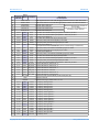
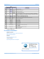
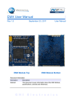
EMX
TM
Module
EMX™ is a combination of hardware (ARM Processor, Flash,
RAM, Ethernet PHY...etc) on a very small (1.55”x1.8”) SMT
OEM 8-Layer board that hosts Microsoft .NET Micro
Framework with various PAL/HAL drivers. In addition to the
benefits of .NET Micro Framework, EMX includes exclusive
software and hardware features, such as support for USB
host, PPP networking and more.
EMX Module is a vastly sophisticated piece of hardware. This
complexity provides the end-user with a remarkably simple
platform to implement in any hardware design. Looking at the
EMX Development System schematic shows just how simple it
really is. All you need is 3.3 volts and some connections to
bring the latest technologies to your products. With
manageable features like USB host and WiFi, the possibilities
are boundless.
What is Microsoft .NET Micro Framework?
Microsoft's .NET Micro Framework extends the advantages Key Features
of .NET and Visual Studio to a class of smaller, less expensive,
● Microsoft .NET Micro Framework
and more resource-constrained devices than the .NET
● 72Mhz 32-bit Processor
Compact Framework or the standard .NET framework.
● 16MB RAM
● 4.5MB FLASH
● Embedded LCD controller
Extended NETMF Features
● Embedded Ethernet PHY with
EMX supports a complete set of .NET Micro Framework
DMA communication.
features such as TCP/IP, SSL, FAT, USB device and more.
● Runtime Loadable Procedure
Including support for other exclusive GHI features such as full
● Full TCP/IP Stack
USB host stack (access thumb drives, mice, keyboards,
● SSL
printers and many other USB devices), CAN, ADC, DAC,PPP,
● ZG2100 WiFi Driver
GPRS, 3G...etc.
● PPP ( GPRS/ 3G )
● DPWS
EMX is also protected against firmware or user application
● Embedded USB host/device
piracy.
● 76 GPIO Pins
● 39 Interrupt Inputs
● 2 SPI (8/16bit)
Runtime Loadable Procedure (RLP)
● I2C
A very useful and unique feature in EMX is allowing users to
● 4 UART
load their own compiled native code (C or assembly) and run it
● 2 CAN Channels
directly through managed Micro Framework. Similar to the use
● 7 10-bit Analog Inputs.
of DLLs on PCs and usually used to implement high● 10-bit Analog Output
processing and time-critical routines.
● 4-bit SD/MMC Memory card
interface
● 6 PWM
Upgrading from Original Embedded Master Module
● 160 mA current consumption with
everything enabled
EMX Module is designed to be compatible with the original
● 40mA Hibernate Mode
Embedded Master Module based designs. We also provide an
● -40ºC to +85ºC Operational
“EM vs EMX” document that points out the differences.
● RoHS Lead Free
GHI Electronics,LLC
EMX Module
Block Diagram
.NET and GHI
Managed Library
GHI RLP
loader
.NET Micro Framework
CLR
PAL
EMX Module
Hardware
16 MB SDRAM
User Runtime Loadable
Procedure (compiled C or
assembly) region
User Managed
Code
4.5MB Flash
HAL
GHI Extended features:
USB Drivers, Hardware Access
LPC2478 72 MHz ARM7
Peripherals:
Digital IOs, Interrupts,
PWM, A/D,
USB HC, USB Device,
MCI,LCD Controller,
Ethernet Controller ...etc
10/100
Ethernet PHY
Getting Started with EMX Modules
GHI Electronics offers a development system for EMX Modules. The development system
exposes every peripheral and includes a 320x240 3.5" display with touch screen. We
highly recommend starting with the development system. With this option, you will have a
running system out-of-the-box.
Copyright © 2010 GHI Electronics, LLC
www.ghielectronics.com
GHI Electronics,LLC
EMX Module
EMX Module Pin-out
Pins marked with IOxx are general purpose digital I/O. These pins might have other features.
Name
No.
1
LPC2478 EMX IO 2nd Feature
H/W Name
3.3V
Connect to 3.3 volt source.
2
GND
IO0*
EMX Module
Pin Description
Connect to Ground.
3
P0.4
4
P0.5
IO1*
5
P0.3
IO2 *
6
P0.2
IO3*
7
P2.5
IO4*
8
P0.24
IO5*
9
P0.25
IO6*
10
P0.26
IO7*
11
P0.23
IO8*
12
P4.29
IO9
13
P4.28
IO10
Piezo
14
P0.28
IO11*
I2C
(open drain pin) I2C Interface SCL
15
P0.27
IO12*
I2C
(open drain pin) I2C Interface SDA
16
P3.16
IO13
PWM0
PWM0 (Pulse Width Modulation Output) LPC2478 PWM Timer 0.
17
P3.24
IO14
PWM1
PWM1 (Pulse Width Modulation Output) LPC2478 PWM Timer 1.
18
P3.25
IO15
N/A
General purpose digital I/O
19
P1.19
IO16
N/A
General purpose digital I/O
20
P2.21
IO17*
N/A
General purpose digital I/O
21
P0.11
IO18*
N/A
General purpose digital I/O
22
P2.22
IO19*
N/A
General purpose digital I/O
23
P0.1
IO20*
CAN1
24
P0.10
IO21*
N/A
25
P0.0
IO22*
CAN1
26
P1.30
N/A
27
P2.10
IO23*
CAN2/
RD CAN Channel 2 Data Receive pin (In) and TinyBooter/Firmware Down Button
Down Button (Check hardware design consideration).
CAN2
TD CAN Channel 2 Data Transmit pin (Out).
COM1
Serial port (UART) RXD receive signal (In) for COM1.
COM1
Serial port (UART) TXD transmit signal (Out) for COM1.
UP Button General purpose digital I/O
and TinyBooter/Firmware Up Button (Check hardware design consideration).
ADC1/
ADC1 (10Bit Analog to Digital Input)
Touch_Y_UP or Touch Screen Y-axis Up analog signal.
ADC2/
ADC2 (10Bit Analog to Digital Input)
COM4
or Serial port (UART) TXD transmit signal (Out) for COM4.
ADC3/ DAC/ ADC3 (10Bit Analog to Digital Input) or DAC (Digital to Analog Output)
COM4
or Serial port (UART) RXD receive signal (In) for COM4.
ADC0/
ADC0 (10Bit Analog to Digital Input)
Touch_X_Left or Touch Screen X-axis Left analog signal.
N/A
General purpose digital I/O
Piezo hardware control.
TD CAN Channel 1 Data Transmit pin (Out)
General purpose digital I/O.
RD CAN Channel 1 Data Receive pin (In)
1
USB_VBUS USB device power detect signal. Connect to power pin on USB device.
N/A
General purpose digital I/O
28
RTC_VBAT
29
USBD- USB Host Feature
Connect to 3.3 volt backup battery to keep the real-time clock running.
USB negative data line of the USB hosting feature.
30
USBD+ USB Host Feature
USB positive data line of the USB hosting feature.
31
P0.12
IO45*
ADC6
ADC6 (10Bit Analog to Digital Input).
32
P0.13
IO46*
ADC7
ADC7 (10Bit Analog to Digital Input).
33
P1.31
IO47
ADC5
ADC5 (10Bit Analog to Digital Input).
34
35
3.3V
P3.27
IO48
Connect to 3.3 volt source.
PWM4
PWM4 (Pulse Width Modulation Output) LPC2478 PWM Timer 1.
36
GND
Connect to Ground.
37
3.3V
Connect to 3.3 volt source.
38
39
P3.26
N/C
IO49
PWM3
Not Connected.
PWM3 (Pulse Width Modulation Output) LPC2478 PWM Timer 1.
40
P3.17
IO50
PWM2
PWM2 (Pulse Width Modulation Output) LPC2478 PWM Timer 0.
Copyright © 2010 GHI Electronics, LLC
www.ghielectronics.com
GHI Electronics,LLC
EMX Module
Name
No.
41
LPC2478 EMX IO 2nd Feature
EMX Module
H/W Name
Pin Description
USBD- device
USB negative data line of the USB debugging interface and for the USB client feature.
42
USBD+ device
43
Ethernet RD-
Ethernet receive data minus.
44
Ethernet RD+
Ethernet receive data plus.
45
Ethernet TD-
Ethernet transmit data minus.
46
USB positive data line of the USB debugging interface and for the USB client feature.
Ethernet TD+
Ethernet transmit data plus.
Recommended Ethernet connector is
J0011D01BNL.
Ethernet PHY is not needed since it is
embedded in EMX hardware.
47
P0.18
IO24*
SPI1
SPI master bus interface MOSI signal (Master Out Slave In) for SPI1.
48
P0.17
IO25*
SPI1
SPI master bus interface MISO signal (Master In Slave Out) for SPI1.
49
P0.16
IO26*
N/A
General purpose digital I/O.
50
P0.15
IO27*
SPI1
SPI master bus interface SCK signal (Clock)for SPI1.
51
P4.23
IO28
COM3
Serial port (UART) RXD receive signal (In) for COM3.
52
P4.22
IO29
COM3
Serial port (UART) TXD transmit signal (Out) for COM3.
53
P2.11
54
P3.30
IO30* Select Button General purpose digital I/O
and TinyBooter/Firmware Select Button (Check hardware design consideration).
IO31
COM2
Serial port (UART) RTS hardware handshaking signal for COM2.
55
P2.1
IO32*
56
P0.6
IO33*
N/A
57
P3.18
IO34
COM2
58
P0.7
IO35*
SPI2
SPI master bus interface SCK signal (Clock)for SPI2.
59
P0.9
IO36*
SPI2
SPI master bus interface MOSI signal (Master Out Slave In) for SPI2.
60
P2.0
IO37*
COM2
61
P0.8
IO38*
SPI2
62
P1.12
IO39
SD_DAT3
SD card 4Bit data bus, data line no. 3.
63
P1.11
IO40
SD_DAT2
SD card 4Bit data bus, data line no. 2.
64
P1.7
IO41
SD_DAT1
SD card 4Bit data bus, data line no. 1.
65
P1.2
IO42
SD_CLK
SD card 4Bit data bus, clock line.
66
P1.6
IO43
SD_DAT0
SD card 4Bit data bus, data line no. 0.
67
P1.3
IO44
SD_CMD
SD card 4Bit data bus, command line.
68
SD_PWR
69
GND
70
RESET#
COM2
Serial port (UART) RXD receive signal (IN) for COM2.
General purpose digital I/O.
Serial port (UART) CTS hardware handshaking signal for COM2.
Serial port (UART) TXD transmit signal (Out) for COM2.
SPI master bus interface MISO signal (Master In Slave Out) for SPI2.
SD memory power (connect directly to SD socket power pin).
Connect to Ground.
Hardware reset signal, Reset state is on Low.
T1
P2.12
IO69*
LCD R0
TFT Display, Red signal bit 0.
T2
P2.6
IO65*
LCD R1
TFT Display, Red signal bit 1.
T3
P2.7
IO66*
LCD R2
TFT Display, Red signal bit 2.
T4
P2.8
IO67*
LCD R3
TFT Display, Red signal bit 3.
T5
P2.9
IO68*
LCD R4
TFT Display, Red signal bit 4.
T6
P1.20
IO51
LCD G0
TFT Display, Green signal bit 0.
T7
P1.21
IO52
LCD G1
TFT Display, Green signal bit 1.
T8
P1.22
IO53
LCD G2
TFT Display, Green signal bit 2.
T9
P1.23
IO54
LCD G3
TFT Display, Green signal bit 3.
T10
P1.24
IO55
LCD G4
TFT Display, Green signal bit 4.
T11
P1.25
IO56
LCD G5
TFT Display, Green signal bit 5.
T12
P2.13
IO70*
LCD B0
TFT Display, Blue signal bit 0.
T13
P1.26
IO57
LCD B1
TFT Display, Blue signal bit 1.
T14
P1.27
IO58
LCD B2
TFT Display, Blue signal bit 2.
T15
P1.28
IO59
LCD B3
TFT Display, Blue signal bit 3.
T16
P1.29
IO60
LCD B4
TFT Display, Blue signal bit 4.
T17
P2.2
IO61*
LCD CLK
TFT Display, Clock.
Copyright © 2010 GHI Electronics, LLC
www.ghielectronics.com
GHI Electronics,LLC
EMX Module
Name
LPC2478 EMX IO 2nd Feature
H/W Name
T18
P2.4
IO63*
LCD EN TFT Display, Enable.
No.
EMX Module
Pin Description
T19
P2.5
IO64*
T20
P2.3
IO62*
LCD
H-Sync
LCD
V-Sync
ALARM
J2
P3.23
IO71
LMODE
J3
P2.23
IO72*
General purpose digital I/O is used to choose the access interface for EMX between
USB (Low) or COM1(High or not connected) on startup (refer to EMX access interface
section).
T_X_Right Touch Screen X-axis Right digital output signal.
J4
P3.31
IO73
T_Y_Down Touch Screen Y-axis Down digital output signal.
J5
P3.29
IO74
PWM5
J6
P4.31
IO75
N/A
J1
TFT Display, Horizontal sync.
TFT Display, Vertical sync.
Leave unconnected (future use)
PWM5 (Pulse Width Modulation Output) LPC2478 PWM Timer 1 .
General purpose digital I/O
J7
JTAG TMS
JTAG TMS signal.
J8
JTAG TCK
JTAG TCK signal.
J9
JTAG TDO
JTAG TDO signal.
J10
JTAG TRST
JTAG TRST signal.
J11
JTAG RTCK
JTAG RTCK signal.
J12
JTAG TDI
J13
Ethernet Speed
J14
Ethernet Link
J15
GND
JTAG TDI signal.
Connect to Ethernet Connector Speed LED.
High = 100 Mbps
Low = 10 Mbps
Connect to Ethernet Connector Link LED.
High = Ethernet activity.
Connect to Ground.
* Interrupt capable input.
For further Information:
Related Documents:
EMX Development System Brochure and Pinout
EMX Module User Manual
Weblinks:
http://www.ghielectronics.com/
Customer Support:
http://www.ghielectronics.com/support
51410 Milano Dr. Suite 114
Macomb Township, MI 48042
United States
PH: +1 586 693 2696
FAX: +1 586 693 3449
www.ghielectronics.com
Copyright © 2010 GHI Electronics, LLC
www.ghielectronics.com
Mouser Electronics
Authorized Distributor
Click to View Pricing, Inventory, Delivery & Lifecycle Information:
GHI Electronics:
EMX10-SM-128