1
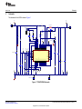
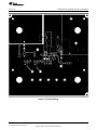
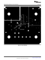
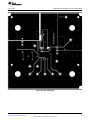
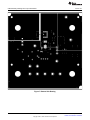
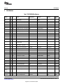
User's Guide
SLVU968 – September 2013
TPS2475XEVM-546 EVM: Evaluation Module for TPS2475X
This user’s guide describes the evaluation module (EVM) for the TPS24750 and TPS24751
(TPS2475XEVM-546). The TPS2475X is a 2.5-V to 18-V power-limiting, hot-swap controller with an
integrated MOSFET cable of high-current operation.
1
2
3
4
5
6
Contents
Introduction .................................................................................................................. 2
1.1
Features ............................................................................................................. 2
1.2
Applications ......................................................................................................... 2
Description ................................................................................................................... 2
Schematic .................................................................................................................... 3
General Configuration and Description .................................................................................. 4
4.1
Physical Access .................................................................................................... 4
4.2
Test Setup .......................................................................................................... 5
EVM Assembly Drawings and Layout Guidelines ...................................................................... 6
5.1
PCB Drawings ...................................................................................................... 6
Bill of Materials ............................................................................................................. 11
List of Figures
1
TPS2475XEVM Schematic ................................................................................................
3
2
Typical TPS2475XEVM Test Setup ......................................................................................
5
3
Top Side Placement ........................................................................................................
6
4
Top Side Routing
...........................................................................................................
7
5
Layer 2 Routing .............................................................................................................
8
6
Layer 3 Routing .............................................................................................................
9
7
Bottom Side Routing ......................................................................................................
10
1
TPS2475X EVM Options ...................................................................................................
2
2
Connector Functionality ....................................................................................................
4
3
Test Points ...................................................................................................................
4
4
Jumpers and LEDs
5
TPS2475XEVM Bill of Materials
.........................................................................................................
........................................................................................
11
List of Tables
SLVU968 – September 2013
Submit Documentation Feedback
TPS2475XEVM-546 EVM: Evaluation Module for TPS2475X
Copyright © 2013, Texas Instruments Incorporated
4
1
Introduction
1
www.ti.com
Introduction
The TPS2475XEVM allows reference circuit evaluation of TI's TPS24750 and TPS24751 hot-swap
controllers with integrated 10-A MOSFET. The TPS2475X is available with both latching and auto-retry
operation.
1.1
Features
•
•
•
•
•
•
1.2
Applications
•
•
•
2
General TPS2475X Features
– 2.5-V to 18.0-V (TYP) bus operation
– Programmable current limit
– Programmable undervoltage lockout
– Programmable overvoltage
– Programmable VOUT slew rate
– Programmable power limit
– Latched-off TPS24750RUV
– Auto-Retry TPS24751RUV
External blocking FET
Push button RESET signal
Copper pour with vias to the internal ground takes advantage of the power pad package
On-board transorb is for overvoltage input protection
Common diode at output prevents negative spike when load is removed while powered on
Server
– Plug-in circuit boards
– Redundant array of independent disks (RAID)
– Disk drives
Telecom
– ATCA
– Micro-ATCA
General hot plug
Description
The TPS2475XEVM-546 enables full evaluation of the TPS2475X devices, refer to the schematic shown
in Figure 1. Input power is applied at T1/T3 while T2/T4 provides the output connection to the load.
D4/C1/C7 provides input protection for the TPS2475X (U1) while D5/C3/C4 provides output protection. S1
allows U1 to be RESET or disabled. A power good (PG) indicator is provided by D2 and circuit faults can
be observed with D3.
Table 1. TPS2475X EVM Options
Part Number
Vin Range
UVLO/OVP
Current Limit
(TYP)
Power Limit
(TYP)
Fault
Response
TPS24751RUV (-001)
2.5 V – 18 V
8.4 V/14 V
11 A
21 W
Auto-Retry
TPS24750RUV (-002)
2.5 V – 18 V
8.4 V/14 V
11 A
21 W
Latched
Turn on or inrush slew rate control can be enabled by installing a shunt on J2 and observed at TP3. The
PG and FAULT LED’s (D2 and D3 respectively) can be enabled by installing a shunt on J1. Scaled
channel current can be monitored at TP16 with a scale factor of 16.17 A/V.
2
TPS2475XEVM-546 EVM: Evaluation Module for TPS2475X
Copyright © 2013, Texas Instruments Incorporated
SLVU968 – September 2013
Submit Documentation Feedback
Schematic
www.ti.com
3
Schematic
The schematic for the EVM is shown in Figure 1
TP1
VIN
TP2
VOUT
T1
VIN
R1
J1
LEDS
T2
VOUT
BFET SHORT
0.002
CB35-36-CY
R2
DNP
0.001
1
2
3
CB35-36-CY
Q1
D1
SH-J1
1,2,3
R4
10.0k
PG
D2
Green
C7
22µF
MMSZ4703T1G
16V
7,8
5,6,
4
R3
10.0k
CSD17501Q5A
30V
D6
1N4148W-7-F
FAULT
D3
TP4
Red
TP3
GATE
TP5
R5
130k
TP6
SENSE
TP7
OUT
1
2
3
J2
GATE dV/dT
C1
0.1µF
SH-J2
20
19
OUT
OUT
22
23
24
25
21
OUT
OUT
OUT
OUT
GATE
26
27
DRAIN
SENSE
28
29
VCC
OUT
OUT
18
C2
0.047µF
17
C3
0.1µF
16
15
14
D5
MBRS330T3G
0.5V
13
12
OUT
11
OUT
10
OUT
9
OUT
8
7
6
5
DRAIN
38
C4
470µF
2
1
OUT
DRAIN
GND
OUT
DRAIN
GND
DRAIN
TIMER
R6
10.0k
S1
RESET
30
DRAIN
GND
37
PROG
SET
36
DRAIN
DRAIN
4
35
U1
TPS24751RUV
EN
3
34
GND
GND
33
IMON
32
D4
SMBJ18A-13-F
PGB
TP10
TMR
OV
TP9
PROG
2
TP8
EN
FLTB
31
DNP
C5
1000pF
R8
1.00k
1
R7
51.1
TP11
TP12
R9
15.0k
R10
64.9k
C6
0.047µF
OV
TP15
R11
1.58k
TP13
IMON
TP16
TP14
SET
TP17
COMMON GROUND
T3
CB35-36-CY
T4
CB35-36-CY
Figure 1. TPS2475XEVM Schematic
SLVU968 – September 2013
Submit Documentation Feedback
TPS2475XEVM-546 EVM: Evaluation Module for TPS2475X
Copyright © 2013, Texas Instruments Incorporated
3
General Configuration and Description
www.ti.com
4
General Configuration and Description
4.1
Physical Access
Table 2 lists the TPS2475XEVM connector functionality, Table 3 describes the test point availability and
Table 4 describes the jumper functionality.
Table 2. Connector Functionality
Connector
Label
Description
T1/T3
VIN/GND
T2/T4
VOUT/GND
2.5 V–18 V input to the EVM
2.5 V–18 V output from the EVM
Table 3. Test Points
Test Point
Color
Label
TP1/TP11/TP12
RED/BLK/SM
VIN/GND
TP2/TP14/TP13
RED/BLK/SM
VOUT/GND
Description
2.5 V–18 V input to the EVM
2.5 V–18 V output from the EVM
TP8
WHT
EN
Active high enable input
TP15
WHT
OV
Active high overvoltage input
TP3
WHT
GATE
TP5
WHT
PG
TP4
WHT
FAULT
TP6
ORG
SNS
Sense amplifier inverting input connection
TP7
ORG
OUT
TPS2475X internal MOSFET DRAIN connection (before blocking FET)
TP9
WHT
PROG
TP10
WHT
TMR
Fault timer programming connection
TP17
WHT
SET
Sense amplifier non-inverting input connection
TP16
WHT
IMON
Blocking FET GATE control and slew rate control
Power good test point
Fault test point
Power limiting engine programming connection
Current monitor. Load current = 16.17 × voltage on TP16.
Table 4. Jumpers and LEDs
4
Jumper
Label
J1
J1
J2
RMP
D2 (GREEN)
PG
D3 (RED)
FAULT
Description
Install between pins 1 and 2 to enable D2 and D3
Install between pins 1 and 2 to enable GATE linear ramp control
Power good indicator. LED turns on when the voltage at TP7 (OUT) gets within 120 mV of the
voltage at TP6 (SNS).
Circuit fault indicator. LED turns on when the internal MOSFET is disabled due to a fault
condition.
TPS2475XEVM-546 EVM: Evaluation Module for TPS2475X
Copyright © 2013, Texas Instruments Incorporated
SLVU968 – September 2013
Submit Documentation Feedback
General Configuration and Description
www.ti.com
4.2
Test Setup
Figure 2 shows a typical test setup for the TPS2475XEVM. Connect T1/T3 to the power supply and T2/T4
to the load.
xx
xx
xx
xx
Oscilloscope
x
Voltmeter
x
C IN
UA M/B U H
NOITAZILITU %
BA T
F I
CL
R ET N E
NUR
ER
BK
DG
AJ
T N I RP
9O
8N
P LE H
DG
DG
DG
A HP LA
3U
2T
DG
Z Y XW
.
0V
TF I H S
7M
+
Positive
T1
Positive
Load
T4
D2
T3
D3
Negative
-
DUT
PWR546
S1
Power
Supply
T2
C NB
s/bM4
Negative
Figure 2. Typical TPS2475XEVM Test Setup
SLVU968 – September 2013
Submit Documentation Feedback
TPS2475XEVM-546 EVM: Evaluation Module for TPS2475X
Copyright © 2013, Texas Instruments Incorporated
5
EVM Assembly Drawings and Layout Guidelines
5
EVM Assembly Drawings and Layout Guidelines
5.1
PCB Drawings
www.ti.com
Figure 3 through Figure 7 show component placement and layout of the EVM.
Figure 3. Top Side Placement
6
TPS2475XEVM-546 EVM: Evaluation Module for TPS2475X
Copyright © 2013, Texas Instruments Incorporated
SLVU968 – September 2013
Submit Documentation Feedback
www.ti.com
EVM Assembly Drawings and Layout Guidelines
Figure 4. Top Side Routing
SLVU968 – September 2013
Submit Documentation Feedback
TPS2475XEVM-546 EVM: Evaluation Module for TPS2475X
Copyright © 2013, Texas Instruments Incorporated
7
EVM Assembly Drawings and Layout Guidelines
www.ti.com
Figure 5. Layer 2 Routing
8
TPS2475XEVM-546 EVM: Evaluation Module for TPS2475X
Copyright © 2013, Texas Instruments Incorporated
SLVU968 – September 2013
Submit Documentation Feedback
www.ti.com
EVM Assembly Drawings and Layout Guidelines
Figure 6. Layer 3 Routing
SLVU968 – September 2013
Submit Documentation Feedback
TPS2475XEVM-546 EVM: Evaluation Module for TPS2475X
Copyright © 2013, Texas Instruments Incorporated
9
EVM Assembly Drawings and Layout Guidelines
www.ti.com
Figure 7. Bottom Side Routing
10
TPS2475XEVM-546 EVM: Evaluation Module for TPS2475X
Copyright © 2013, Texas Instruments Incorporated
SLVU968 – September 2013
Submit Documentation Feedback
Bill of Materials
www.ti.com
6
Bill of Materials
Table 5. TPS2475XEVM Bill of Materials
Designator
QTY
Value
Description
Package Reference
Printed Circuit Board
Part Number
Manufacturer
Alternate Part
Number
PCB1
1
PWR546
Any
—
C1, C3
2
0.1uF
CAP, CERM, 0.1uF, 25V, +/-10%, X7R, 0603
0603
06033C104KAT2A
AVX
—
C2
1
0.047uF
CAP, CERM, 0.047uF, 25V, +/-10%, X7R, 0603
0603
C1608X7R1E473K
TDK
C4
1
470uF
CAP, AL, 470uF, 25V, +/-20%, 0.15 ohm, SMD
SMT Radial G
EEE-FC1E471P
Panasonic
C5
1
1000pF
CAP, CERM, 1000pF, 100V, +/-20%, X7R, 0603
0603
06031C102MAT2A
AVX
C6
1
0.047uF
CAP, CERM, 0.047uF, 100V, +/-10%, X7R, 0603
0603
C0603C473K1RACTU
Kemet
C7
1
22uF
CAP, CERM, 22uF, 25V, +/-20%, X5R, 1210
1210
12103D226MAT2A
AVX
D1
1
16V
Diode, Zener, 16V, 500mW, SOD-123
SOD-123
MMSZ4703T1G
ON Semiconductor
D2
1
Green
LED, Green, SMD
Power TOPLED w/lens
LT E63C-CADB-35-L-Z
OSRAM
—
D3
1
Red
LED, Red, SMD
Power TOPLED w/lens
LS E63F-DBFA-1-Z
OSRAM
—
D4
1
18V
Diode, TVS, Uni, 18V, 600W, SMB
SMB
SMBJ18A-13-F
Diodes Inc.
—
D5
1
0.5V
Diode, Schottky, 30V, 3A, SMC
SMC
MBRS330T3G
ON Semiconductor
D6
1
1.25V
Diode, Ultrafast, 100V, 0.15A, SOD-123
SOD-123
1N4148W-7-F
Diodes Inc.
J1, J2
2
1x3
Header, TH, 100mil, 1x3, Gold plated,
230 mil above insulator
PBC03SAAN
PBC03SAAN
Sullins Connector Solutions
LBL1
1
Thermal Transfer Printable Labels,
1.250" W x 0.250" H – 10,000 per roll
PCB Label 1.25"H x 0.250"W
THT-13-457-10
Brady
Q1
1
30V
MOSFET, N-CH, 30V, 100A, SON 5x6mm
SON 5x6mm
CSD17501Q5A
Texas Instruments
R1
1
0.002
RES, 0.002 ohm, 1%, 1W, 2512
2512
ERJ-M1WTF2M0U
Panasonic
R3, R4, R6
3
10.0k
RES, 10.0k ohm, 1%, 0.1W, 0603
0603
CRCW060310K0FKEA
Vishay-Dale
R5
1
130k
RES, 130k ohm, 1%, 0.1W, 0603
0603
CRCW0603130KFKEA
Vishay-Dale
R7
1
51.1
RES, 51.1 ohm, 1%, 0.1W, 0603
0603
CRCW060351R1FKEA
Vishay-Dale
R8
1
1.00k
RES, 1.00k ohm, 1%, 0.1W, 0603
0603
CRCW06031K00FKEA
Vishay-Dale
R9
1
15.0k
RES, 15.0k ohm, 1%, 0.1W, 0603
0603
CRCW060315K0FKEA
Vishay-Dale
R10
1
64.9k
RES, 64.9k ohm, 1%, 0.1W, 0603
0603
CRCW060364K9FKEA
Vishay-Dale
R11
1
1.58k
RES, 1.58k ohm, 1%, 0.1W, 0603
0603
CRCW06031K58FKEA
Vishay-Dale
S1
1
Switch, Push Button, SMD
2.9x2x3.9mm SMD
SKRKAEE010
Alps
Equivalent
SH-J1
1
1x2
Shunt, 100mil, Gold plated, Black
Shunt
969102-0000-DA
3M
SNT-100-BK-G
T1–T4
4
50A
Terminal 50A Lug
CB35-36-CY
CB35-36-CY
Panduit
TP1, TP2
2
Red
Test Point, TH, Multipurpose, Red
Keystone5010
5010
Keystone
Equivalent
TP3–TP5,
TP8–TP10,
TP15–TP17
9
White
Test Point, TH, Multipurpose, White
Keystone5012
5012
Keystone
Equivalent
TP6, TP7
2
Orange
Test Point, TH, Multipurpose, Orange
Keystone5013
5013
Keystone
Equivalent
TP11, TP14
2
Black
Test Point, TH, Multipurpose, Black
Keystone5011
5011
Keystone
Equivalent
SLVU968 – September 2013
Submit Documentation Feedback
—
Equivalent
TPS2475XEVM-546 EVM: Evaluation Module for TPS2475X
Copyright © 2013, Texas Instruments Incorporated
11
Bill of Materials
www.ti.com
Table 5. TPS2475XEVM Bill of Materials (continued)
Designator
QTY
Value
Description
Package Reference
Part Number
Manufacturer
TP12, TP13
2
SMT
Test Point, SMT, Compact
Testpoint_Keystone_Compact
5016
Keystone
U1
1
2.5 to 18 V Positive Voltage 10A Integrated HotSwap Controller, RUV0036A
RUV0036A
TPS24750RUV or TPS24751RUV
Texas Instruments
FID1, FID2, FID3
0
Fiducial mark. There is nothing to buy or mount.
Fiducial
N/A
N/A
R2
0
0.001
RES, 0.001 ohm, 1%, 1W, 1210
1210
PMR25HZPFV1L00
Rohm
SH-J2
0
1x2
Shunt, 100mil, Gold plated, Black
Shunt
969102-0000-DA
3M
Alternate Part
Number
SNT-100-BK-G
NOTE: Unless otherwise noted in the alternate part number or alternate manufacturer columns, all parts may be substituted with equivalents.
12
TPS2475XEVM-546 EVM: Evaluation Module for TPS2475X
SLVU968 – September 2013
Submit Documentation Feedback
Copyright © 2013, Texas Instruments Incorporated
EVALUATION BOARD/KIT/MODULE (EVM) ADDITIONAL TERMS
Texas Instruments (TI) provides the enclosed Evaluation Board/Kit/Module (EVM) under the following conditions:
The user assumes all responsibility and liability for proper and safe handling of the goods. Further, the user indemnifies TI from all claims
arising from the handling or use of the goods.
Should this evaluation board/kit not meet the specifications indicated in the User’s Guide, the board/kit may be returned within 30 days from
the date of delivery for a full refund. THE FOREGOING LIMITED WARRANTY IS THE EXCLUSIVE WARRANTY MADE BY SELLER TO
BUYER AND IS IN LIEU OF ALL OTHER WARRANTIES, EXPRESSED, IMPLIED, OR STATUTORY, INCLUDING ANY WARRANTY OF
MERCHANTABILITY OR FITNESS FOR ANY PARTICULAR PURPOSE. EXCEPT TO THE EXTENT OF THE INDEMNITY SET FORTH
ABOVE, NEITHER PARTY SHALL BE LIABLE TO THE OTHER FOR ANY INDIRECT, SPECIAL, INCIDENTAL, OR CONSEQUENTIAL
DAMAGES.
Please read the User's Guide and, specifically, the Warnings and Restrictions notice in the User's Guide prior to handling the product. This
notice contains important safety information about temperatures and voltages. For additional information on TI's environmental and/or safety
programs, please visit www.ti.com/esh or contact TI.
No license is granted under any patent right or other intellectual property right of TI covering or relating to any machine, process, or
combination in which such TI products or services might be or are used. TI currently deals with a variety of customers for products, and
therefore our arrangement with the user is not exclusive. TI assumes no liability for applications assistance, customer product design,
software performance, or infringement of patents or services described herein.
REGULATORY COMPLIANCE INFORMATION
As noted in the EVM User’s Guide and/or EVM itself, this EVM and/or accompanying hardware may or may not be subject to the Federal
Communications Commission (FCC) and Industry Canada (IC) rules.
For EVMs not subject to the above rules, this evaluation board/kit/module is intended for use for ENGINEERING DEVELOPMENT,
DEMONSTRATION OR EVALUATION PURPOSES ONLY and is not considered by TI to be a finished end product fit for general consumer
use. It generates, uses, and can radiate radio frequency energy and has not been tested for compliance with the limits of computing
devices pursuant to part 15 of FCC or ICES-003 rules, which are designed to provide reasonable protection against radio frequency
interference. Operation of the equipment may cause interference with radio communications, in which case the user at his own expense will
be required to take whatever measures may be required to correct this interference.
General Statement for EVMs including a radio
User Power/Frequency Use Obligations: This radio is intended for development/professional use only in legally allocated frequency and
power limits. Any use of radio frequencies and/or power availability of this EVM and its development application(s) must comply with local
laws governing radio spectrum allocation and power limits for this evaluation module. It is the user’s sole responsibility to only operate this
radio in legally acceptable frequency space and within legally mandated power limitations. Any exceptions to this are strictly prohibited and
unauthorized by Texas Instruments unless user has obtained appropriate experimental/development licenses from local regulatory
authorities, which is responsibility of user including its acceptable authorization.
For EVMs annotated as FCC – FEDERAL COMMUNICATIONS COMMISSION Part 15 Compliant
Caution
This device complies with part 15 of the FCC Rules. Operation is subject to the following two conditions: (1) This device may not cause
harmful interference, and (2) this device must accept any interference received, including interference that may cause undesired operation.
Changes or modifications not expressly approved by the party responsible for compliance could void the user's authority to operate the
equipment.
FCC Interference Statement for Class A EVM devices
This equipment has been tested and found to comply with the limits for a Class A digital device, pursuant to part 15 of the FCC Rules.
These limits are designed to provide reasonable protection against harmful interference when the equipment is operated in a commercial
environment. This equipment generates, uses, and can radiate radio frequency energy and, if not installed and used in accordance with the
instruction manual, may cause harmful interference to radio communications. Operation of this equipment in a residential area is likely to
cause harmful interference in which case the user will be required to correct the interference at his own expense.
FCC Interference Statement for Class B EVM devices
This equipment has been tested and found to comply with the limits for a Class B digital device, pursuant to part 15 of the FCC Rules.
These limits are designed to provide reasonable protection against harmful interference in a residential installation. This equipment
generates, uses and can radiate radio frequency energy and, if not installed and used in accordance with the instructions, may cause
harmful interference to radio communications. However, there is no guarantee that interference will not occur in a particular installation. If
this equipment does cause harmful interference to radio or television reception, which can be determined by turning the equipment off and
on, the user is encouraged to try to correct the interference by one or more of the following measures:
• Reorient or relocate the receiving antenna.
• Increase the separation between the equipment and receiver.
• Connect the equipment into an outlet on a circuit different from that to which the receiver is connected.
• Consult the dealer or an experienced radio/TV technician for help.
For EVMs annotated as IC – INDUSTRY CANADA Compliant
This Class A or B digital apparatus complies with Canadian ICES-003.
Changes or modifications not expressly approved by the party responsible for compliance could void the user’s authority to operate the
equipment.
Concerning EVMs including radio transmitters
This device complies with Industry Canada licence-exempt RSS standard(s). Operation is subject to the following two conditions: (1) this
device may not cause interference, and (2) this device must accept any interference, including interference that may cause undesired
operation of the device.
Concerning EVMs including detachable antennas
Under Industry Canada regulations, this radio transmitter may only operate using an antenna of a type and maximum (or lesser) gain
approved for the transmitter by Industry Canada. To reduce potential radio interference to other users, the antenna type and its gain should
be so chosen that the equivalent isotropically radiated power (e.i.r.p.) is not more than that necessary for successful communication.
This radio transmitter has been approved by Industry Canada to operate with the antenna types listed in the user guide with the maximum
permissible gain and required antenna impedance for each antenna type indicated. Antenna types not included in this list, having a gain
greater than the maximum gain indicated for that type, are strictly prohibited for use with this device.
Cet appareil numérique de la classe A ou B est conforme à la norme NMB-003 du Canada.
Les changements ou les modifications pas expressément approuvés par la partie responsable de la conformité ont pu vider l’autorité de
l'utilisateur pour actionner l'équipement.
Concernant les EVMs avec appareils radio
Le présent appareil est conforme aux CNR d'Industrie Canada applicables aux appareils radio exempts de licence. L'exploitation est
autorisée aux deux conditions suivantes : (1) l'appareil ne doit pas produire de brouillage, et (2) l'utilisateur de l'appareil doit accepter tout
brouillage radioélectrique subi, même si le brouillage est susceptible d'en compromettre le fonctionnement.
Concernant les EVMs avec antennes détachables
Conformément à la réglementation d'Industrie Canada, le présent émetteur radio peut fonctionner avec une antenne d'un type et d'un gain
maximal (ou inférieur) approuvé pour l'émetteur par Industrie Canada. Dans le but de réduire les risques de brouillage radioélectrique à
l'intention des autres utilisateurs, il faut choisir le type d'antenne et son gain de sorte que la puissance isotrope rayonnée équivalente
(p.i.r.e.) ne dépasse pas l'intensité nécessaire à l'établissement d'une communication satisfaisante.
Le présent émetteur radio a été approuvé par Industrie Canada pour fonctionner avec les types d'antenne énumérés dans le manuel
d’usage et ayant un gain admissible maximal et l'impédance requise pour chaque type d'antenne. Les types d'antenne non inclus dans
cette liste, ou dont le gain est supérieur au gain maximal indiqué, sont strictement interdits pour l'exploitation de l'émetteur.
SPACER
SPACER
SPACER
SPACER
SPACER
SPACER
SPACER
SPACER
【Important Notice for Users of EVMs for RF Products in Japan】
】
This development kit is NOT certified as Confirming to Technical Regulations of Radio Law of Japan
If you use this product in Japan, you are required by Radio Law of Japan to follow the instructions below with respect to this product:
1.
2.
3.
Use this product in a shielded room or any other test facility as defined in the notification #173 issued by Ministry of Internal Affairs and
Communications on March 28, 2006, based on Sub-section 1.1 of Article 6 of the Ministry’s Rule for Enforcement of Radio Law of
Japan,
Use this product only after you obtained the license of Test Radio Station as provided in Radio Law of Japan with respect to this
product, or
Use of this product only after you obtained the Technical Regulations Conformity Certification as provided in Radio Law of Japan with
respect to this product. Also, please do not transfer this product, unless you give the same notice above to the transferee. Please note
that if you could not follow the instructions above, you will be subject to penalties of Radio Law of Japan.
Texas Instruments Japan Limited
(address) 24-1, Nishi-Shinjuku 6 chome, Shinjuku-ku, Tokyo, Japan
http://www.tij.co.jp
【無線電波を送信する製品の開発キットをお使いになる際の注意事項】
本開発キットは技術基準適合証明を受けておりません。
本製品のご使用に際しては、電波法遵守のため、以下のいずれかの措置を取っていただく必要がありますのでご注意ください。
1.
2.
3.
電波法施行規則第6条第1項第1号に基づく平成18年3月28日総務省告示第173号で定められた電波暗室等の試験設備でご使用いただく。
実験局の免許を取得後ご使用いただく。
技術基準適合証明を取得後ご使用いただく。
なお、本製品は、上記の「ご使用にあたっての注意」を譲渡先、移転先に通知しない限り、譲渡、移転できないものとします。
上記を遵守頂けない場合は、電波法の罰則が適用される可能性があることをご留意ください。
日本テキサス・インスツルメンツ株式会社
東京都新宿区西新宿6丁目24番1号
西新宿三井ビル
http://www.tij.co.jp
SPACER
SPACER
SPACER
SPACER
SPACER
SPACER
SPACER
SPACER
SPACER
SPACER
SPACER
SPACER
SPACER
SPACER
SPACER
SPACER
SPACER
EVALUATION BOARD/KIT/MODULE (EVM)
WARNINGS, RESTRICTIONS AND DISCLAIMERS
For Feasibility Evaluation Only, in Laboratory/Development Environments. Unless otherwise indicated, this EVM is not a finished
electrical equipment and not intended for consumer use. It is intended solely for use for preliminary feasibility evaluation in
laboratory/development environments by technically qualified electronics experts who are familiar with the dangers and application risks
associated with handling electrical mechanical components, systems and subsystems. It should not be used as all or part of a finished end
product.
Your Sole Responsibility and Risk. You acknowledge, represent and agree that:
1.
2.
3.
4.
You have unique knowledge concerning Federal, State and local regulatory requirements (including but not limited to Food and Drug
Administration regulations, if applicable) which relate to your products and which relate to your use (and/or that of your employees,
affiliates, contractors or designees) of the EVM for evaluation, testing and other purposes.
You have full and exclusive responsibility to assure the safety and compliance of your products with all such laws and other applicable
regulatory requirements, and also to assure the safety of any activities to be conducted by you and/or your employees, affiliates,
contractors or designees, using the EVM. Further, you are responsible to assure that any interfaces (electronic and/or mechanical)
between the EVM and any human body are designed with suitable isolation and means to safely limit accessible leakage currents to
minimize the risk of electrical shock hazard.
Since the EVM is not a completed product, it may not meet all applicable regulatory and safety compliance standards (such as UL,
CSA, VDE, CE, RoHS and WEEE) which may normally be associated with similar items. You assume full responsibility to determine
and/or assure compliance with any such standards and related certifications as may be applicable. You will employ reasonable
safeguards to ensure that your use of the EVM will not result in any property damage, injury or death, even if the EVM should fail to
perform as described or expected.
You will take care of proper disposal and recycling of the EVM’s electronic components and packing materials.
Certain Instructions. It is important to operate this EVM within TI’s recommended specifications and environmental considerations per the
user guidelines. Exceeding the specified EVM ratings (including but not limited to input and output voltage, current, power, and
environmental ranges) may cause property damage, personal injury or death. If there are questions concerning these ratings please contact
a TI field representative prior to connecting interface electronics including input power and intended loads. Any loads applied outside of the
specified output range may result in unintended and/or inaccurate operation and/or possible permanent damage to the EVM and/or
interface electronics. Please consult the EVM User's Guide prior to connecting any load to the EVM output. If there is uncertainty as to the
load specification, please contact a TI field representative. During normal operation, some circuit components may have case temperatures
greater than 60°C as long as the input and output are maintained at a normal ambient operating temperature. These components include
but are not limited to linear regulators, switching transistors, pass transistors, and current sense resistors which can be identified using the
EVM schematic located in the EVM User's Guide. When placing measurement probes near these devices during normal operation, please
be aware that these devices may be very warm to the touch. As with all electronic evaluation tools, only qualified personnel knowledgeable
in electronic measurement and diagnostics normally found in development environments should use these EVMs.
Agreement to Defend, Indemnify and Hold Harmless. You agree to defend, indemnify and hold TI, its licensors and their representatives
harmless from and against any and all claims, damages, losses, expenses, costs and liabilities (collectively, "Claims") arising out of or in
connection with any use of the EVM that is not in accordance with the terms of the agreement. This obligation shall apply whether Claims
arise under law of tort or contract or any other legal theory, and even if the EVM fails to perform as described or expected.
Safety-Critical or Life-Critical Applications. If you intend to evaluate the components for possible use in safety critical applications (such
as life support) where a failure of the TI product would reasonably be expected to cause severe personal injury or death, such as devices
which are classified as FDA Class III or similar classification, then you must specifically notify TI of such intent and enter into a separate
Assurance and Indemnity Agreement.
Mailing Address: Texas Instruments, Post Office Box 655303, Dallas, Texas 75265
Copyright © 2013, Texas Instruments Incorporated
IMPORTANT NOTICE
Texas Instruments Incorporated and its subsidiaries (TI) reserve the right to make corrections, enhancements, improvements and other
changes to its semiconductor products and services per JESD46, latest issue, and to discontinue any product or service per JESD48, latest
issue. Buyers should obtain the latest relevant information before placing orders and should verify that such information is current and
complete. All semiconductor products (also referred to herein as “components”) are sold subject to TI’s terms and conditions of sale
supplied at the time of order acknowledgment.
TI warrants performance of its components to the specifications applicable at the time of sale, in accordance with the warranty in TI’s terms
and conditions of sale of semiconductor products. Testing and other quality control techniques are used to the extent TI deems necessary
to support this warranty. Except where mandated by applicable law, testing of all parameters of each component is not necessarily
performed.
TI assumes no liability for applications assistance or the design of Buyers’ products. Buyers are responsible for their products and
applications using TI components. To minimize the risks associated with Buyers’ products and applications, Buyers should provide
adequate design and operating safeguards.
TI does not warrant or represent that any license, either express or implied, is granted under any patent right, copyright, mask work right, or
other intellectual property right relating to any combination, machine, or process in which TI components or services are used. Information
published by TI regarding third-party products or services does not constitute a license to use such products or services or a warranty or
endorsement thereof. Use of such information may require a license from a third party under the patents or other intellectual property of the
third party, or a license from TI under the patents or other intellectual property of TI.
Reproduction of significant portions of TI information in TI data books or data sheets is permissible only if reproduction is without alteration
and is accompanied by all associated warranties, conditions, limitations, and notices. TI is not responsible or liable for such altered
documentation. Information of third parties may be subject to additional restrictions.
Resale of TI components or services with statements different from or beyond the parameters stated by TI for that component or service
voids all express and any implied warranties for the associated TI component or service and is an unfair and deceptive business practice.
TI is not responsible or liable for any such statements.
Buyer acknowledges and agrees that it is solely responsible for compliance with all legal, regulatory and safety-related requirements
concerning its products, and any use of TI components in its applications, notwithstanding any applications-related information or support
that may be provided by TI. Buyer represents and agrees that it has all the necessary expertise to create and implement safeguards which
anticipate dangerous consequences of failures, monitor failures and their consequences, lessen the likelihood of failures that might cause
harm and take appropriate remedial actions. Buyer will fully indemnify TI and its representatives against any damages arising out of the use
of any TI components in safety-critical applications.
In some cases, TI components may be promoted specifically to facilitate safety-related applications. With such components, TI’s goal is to
help enable customers to design and create their own end-product solutions that meet applicable functional safety standards and
requirements. Nonetheless, such components are subject to these terms.
No TI components are authorized for use in FDA Class III (or similar life-critical medical equipment) unless authorized officers of the parties
have executed a special agreement specifically governing such use.
Only those TI components which TI has specifically designated as military grade or “enhanced plastic” are designed and intended for use in
military/aerospace applications or environments. Buyer acknowledges and agrees that any military or aerospace use of TI components
which have not been so designated is solely at the Buyer's risk, and that Buyer is solely responsible for compliance with all legal and
regulatory requirements in connection with such use.
TI has specifically designated certain components as meeting ISO/TS16949 requirements, mainly for automotive use. In any case of use of
non-designated products, TI will not be responsible for any failure to meet ISO/TS16949.
Products
Applications
Audio
www.ti.com/audio
Automotive and Transportation
www.ti.com/automotive
Amplifiers
amplifier.ti.com
Communications and Telecom
www.ti.com/communications
Data Converters
dataconverter.ti.com
Computers and Peripherals
www.ti.com/computers
DLP® Products
www.dlp.com
Consumer Electronics
www.ti.com/consumer-apps
DSP
dsp.ti.com
Energy and Lighting
www.ti.com/energy
Clocks and Timers
www.ti.com/clocks
Industrial
www.ti.com/industrial
Interface
interface.ti.com
Medical
www.ti.com/medical
Logic
logic.ti.com
Security
www.ti.com/security
Power Mgmt
power.ti.com
Space, Avionics and Defense
www.ti.com/space-avionics-defense
Microcontrollers
microcontroller.ti.com
Video and Imaging
www.ti.com/video
RFID
www.ti-rfid.com
OMAP Applications Processors
www.ti.com/omap
TI E2E Community
e2e.ti.com
Wireless Connectivity
www.ti.com/wirelessconnectivity
Mailing Address: Texas Instruments, Post Office Box 655303, Dallas, Texas 75265
Copyright © 2013, Texas Instruments Incorporated