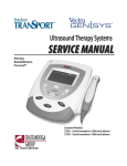
1
User's Guide
SLVUA40A – March 2014 – Revised January 2015
bq500414Q bqTESLA Wireless Power TX EVM
The bqTESLA™ wireless power transmitter evaluation module from Texas Instruments is a highperformance, easy-to-use development module for the design of wireless power solutions. The
bq500414Q EVM evaluation module (EVM) provides all the basic functions of a Qi-compliant three coil, A6
type, wireless charger pad. The EVM is intended to be used with the bq51013BEVM-764 or any other Qicompliant receiver. Both the WPC 1.0 and WPC 1.1 receivers are supported with this design. The
bq500414QEVM-629 is a 12-V input design
1
2
3
4
5
6
7
8
Contents
Applications ................................................................................................................... 2
bq500414QEVM-629 Electrical Performance Specifications .......................................................... 2
Modifications.................................................................................................................. 2
Connector and Test Point Descriptions ................................................................................... 3
4.1
Connector and Test Point Descriptions .......................................................................... 3
4.2
Test Point Descriptions ............................................................................................ 3
Schematic and Bill of Materials ............................................................................................ 6
Test Setup ................................................................................................................... 12
6.1
Equipment .......................................................................................................... 12
6.2
Equipment Setup .................................................................................................. 13
bq500414QEVM-629 Assembly Drawings and Layout ................................................................ 16
Reference ................................................................................................................... 22
List of Figures
1
bq500414QEVM-629 Schematic........................................................................................... 6
2
bq500414QEVM-629 Schematic........................................................................................... 7
3
bq500414QEVM-629 Schematic
4
5
6
7
8
9
10
11
12
.......................................................................................... 8
Equipment Setup ........................................................................................................... 13
Efficiency versus Power, bq500414QEVM-629 Transmitter and HPA764 Receiver .............................. 14
Assembly Top ............................................................................................................... 16
Top Overlay ................................................................................................................. 17
Top Solder................................................................................................................... 18
Top Layer.................................................................................................................... 19
Inner Layer 1 ................................................................................................................ 20
Inner Layer 2 ................................................................................................................ 21
Bottom Layer ................................................................................................................ 22
List of Tables
..........................................................
..............................................................................................................
1
bq500414QEVM-629 Electrical Performance Specifications
2
2
Bill of Materials
9
bqTESLA is a trademark of Texas Instruments.
Avid is a registered trademark of Avid Technology, Inc..
SLVUA40A – March 2014 – Revised January 2015
Submit Documentation Feedback
bq500414Q bqTESLA Wireless Power TX EVM
Copyright © 2014–2015, Texas Instruments Incorporated
1
Applications
1
www.ti.com
Applications
The bq500414QEVM-629 evaluation module demonstrates the transmitter portion of the bqTESLA™
wireless power system. This transmitter EVM is a complete transmitter-side solution that powers a
bqTESLA™ receiver. The EVM requires only input power for operation, 12 Vdc at 1 A. All transmitter-side
electronics and transmitter coils are on a single 4-layer printed-circuit board (PCB). The open design
allows easy access to key points of the electrical schematic.
This EVM has the following features:
• WPC A6-Type transmitter coil, 70 mm × 20 mm free positioning area
• Designed for 12-Vdc systems
• Optional input power SEPIC converter to produce 12 Vdc from 6 V to 16 V
• Fully WPC 1.1 Foreign Object Detection (FOD) and WPC 1.0 Parasitic Metal Object Detection (PMOD)
• Reduced parts count from the legacy bq500410A design
• LED indicates power transfer or power fault state
2
bq500414QEVM-629 Electrical Performance Specifications
Table 1 provides a summary of the EVM performance specifications. All specifications are given for an
ambient temperature of 25°C.
Table 1. bq500414QEVM-629 Electrical Performance Specifications
Parameter
Notes and Conditions
Min
Typ
Max
12
16
Unit
Input Characteristics
VIN
Input voltage bq500414Q
IIN
Input current
VIN = 12 V, RX IOUT = 1 A at 5 V
6
Input no-load current
VIN = 12 V, IOUT = 0 A
Input stand-by current
VIN = 12 V
V
570
mA
72
mA
18.75
mA
Output Characteristics – Receiver bq51013BEVM-764
VOUT
IOUT
Output voltage
VIN = Nom, IOUT = Nom
Output ripple
VIN = Nom, IOUT = Max
VIN = Min to Max
VIN = Min to Max
Output overcurrent
VIN = Nom
4.5
5
5.1
V
200
mVPP
0
1
A
1.1
A
205
kHz
Systems Characteristics
3
FS
Switching frequency
Switching frequency varies with load
ηpk
Peak efficiency
VIN = 12 V, P Out RX = 2.5 W
η
Full-load efficiency
VIN = Nom, IOUT = Max
120
75%
73.6%
Modifications
See the data sheet (SLUSBE4) when changing components.
Use LED mode – resistor R23 to change the behavior of the status LED, D2, D8 and D9. The standard
value is 42.2 kΩ for control option 1, see the datasheet for additional settings.
FOD threshold setting can be changed using R3. If R3 is removed then FOD function is disabled.
PMOD threshold setting can be changed using R22. If R22 is removed then PMOD function is disabled.
FOD_CAL can be used to change the slope of the FOD LOSS curve for better FOD performance, R52.
Addition of EMI Filter Shield, PWR633 to reduce emissions, see section 6.2.2.6
2
bq500414Q bqTESLA Wireless Power TX EVM
SLVUA40A – March 2014 – Revised January 2015
Submit Documentation Feedback
Copyright © 2014–2015, Texas Instruments Incorporated
Connector and Test Point Descriptions
www.ti.com
4
Connector and Test Point Descriptions
This section contains descriptions for the connectors and the test points.
4.1
Connector and Test Point Descriptions
The connection points are described in Section 4.1.1 through Section 4.1.3.
4.1.1
J1 – (Pin 1)VIN, (Pin 2) GND
Pin 1 - Input power 12 Vdc ±500 mV,
Pin 2 - Return for 12Vdc Input (Ground)
4.1.2
J2 – PMBus
Pin 6 - AGND
Pin 9 - PM_CLK
Pin 10 - PM_DATA
4.1.3
J3 –JTAG
Factory use only.
4.1.4
Control Headers
4.1.4.1
JP1 PMOD and FOD Enable / Disable
Shorting Jumper installed = Enable, removed = Disable
4.1.4.2
JP2 LED select bypass
Shorting Jumper installed = LED Bin 0
Default is not installed.
4.2
Test Point Descriptions
The test points are described in Section 4.2.1 through Section 4.2.15.
4.2.1
TP1 – Unused
Reserved – no connection.
4.2.2
TP2 – BUZ_DC
Output from IC to drive DC buzzer, signals start of power transfer.
4.2.3
TP3 – FOD
Select for FOD threshold
4.2.4
TP4 – COIL1.2
Output from bq500414Q, low enables coil 2 drive.
4.2.5
TP5 – PMOD
Select for PMOD threshold
SLVUA40A – March 2014 – Revised January 2015
Submit Documentation Feedback
bq500414Q bqTESLA Wireless Power TX EVM
Copyright © 2014–2015, Texas Instruments Incorporated
3
Connector and Test Point Descriptions
4.2.6
www.ti.com
TP6 – Reserved
Reserved – no connection.
4.2.7
TP7 – Reserved
Reserved – no connection
4.2.8
TP8 – COIL1.3
Output from bq500414Q, low enables coil 3 drive.
4.2.9
TP9 – 12Vdc
System regulated 12V from VIN
4.2.10
TP10 - Reserved
Reserved – no connection
4.2.11
TP11 – Shield / No Shield
Input to configure bq500414Q to operate with EMI shield, PWR633. Low = no shield, high (3.3V) = shield
4.2.12
TP12 – 12Vdc Feedback
Feedback circuit for 12V regulator
4.2.13
TP13 – GND
Ground test point connection
4.2.14
TP14 – I_SENSE
Current as measured in the system 12V supply
4.2.15
TP15 – COMMSample of coil voltage return for communications with RX
4.2.16
TP16 – COMM+
Sample of coil voltage for communications with RX
4.2.17
TP17 – Reserved
Reserved – no connection.
4.2.18
TP18 – DPWM-1A
PWM Output to half bridge drivers
4.2.19
TP19 – Reserved
Reserved – no connection.
4.2.20
TP20 – GND
Ground test point connection
4
bq500414Q bqTESLA Wireless Power TX EVM
SLVUA40A – March 2014 – Revised January 2015
Submit Documentation Feedback
Copyright © 2014–2015, Texas Instruments Incorporated
Connector and Test Point Descriptions
www.ti.com
4.2.21
TP21 – GND
Ground test point connection
4.2.22
TP22 – AGND
Analog ground test point connection
4.2.23
TP23 – COIL1.1
Output from bq500414Q, low enables coil 1 drive.
4.2.24
TP24 – AGND
Analog ground test point connection
4.2.25
TP25 – 3.3Vdc_EN
3.3Vdc enable signal to the regulator
4.2.26
TP26 – EN_PWR
Enable signal for the 12Vdc system regulator
4.2.27
TP27 – PWRGD
Power good signal from the 3.3Vdc regulator
4.2.28
TP28 – TANK3
Coil 3 Resonant Tank Drive Signal
4.2.29
TP29 – PHSE3
Coil 3 Drive signal
4.2.30
TP30 – GND
Ground test point connection
4.2.31
TP31 – PHSE1
Coil 1 Drive signal
4.2.32
TP32 – TANK2
Coil 2 Resonant Tank Drive Signal
4.2.33
TP33 – TANK1
Coil 1 Resonant Tank Drive Signal
4.2.34
TP34 – GND
Ground test point connection
4.2.35
TP35 – PHSE2
Coil 2 Drive signal
SLVUA40A – March 2014 – Revised January 2015
Submit Documentation Feedback
bq500414Q bqTESLA Wireless Power TX EVM
Copyright © 2014–2015, Texas Instruments Incorporated
5
Schematic and Bill of Materials
5
www.ti.com
Schematic and Bill of Materials
This section includes the schematics and bill of materials for the EVM.
Figure 1 illustrates the schematic for this EVM.
VIN_FLTR
Vin = 6 to 16 VDC
L2
L1
2
1
C2
1µF
C6
1µF
TP20 TP21
C18
4.7µF
R13
4.70
C10
4.7µF
GND
12VDC
TP22 TP24
GND
GND
D4
GND
GND
4.7µF
C35
AGND
C37
22µF
R15
10.0
R18
10.0
3
EN_PWR
4
C13
0.22µF
C12
5
SS
BP
DIS/EN
GDRV
COMP
ISNS
FB
11
GND
GND
1µF
GND
4.70
10
9
Q1
U9
INA213-Q1
BSZ0902NS
1
2
C7 1µF
REF
V+
GND
3V3_VCC
3
C30
0.01µF
6
VDD
270pF
R29
GND
RC
PWPD
2
GND
5
U1
TPS40210DGQ
TP26
GND
IN-
R11
205k
4.7µF
4
C8
1µF
1
GND
VIN_BRD
0.04
C11
22µF
C40
R14
NoPop
R51
100k
R64
B560C
Net-Tie
3V3_VCC
12VDC
C34
IN+
Gnd
OUT
Vin
J1
AGND
8
R26
7
R62
AGND
1.00k
1.00k
6
C9
270pF
R30
0.025
I_SENSE
TP14
TP9
GND
C57
0.1µF
GND
GND
R50
49.9
GND
C17
TP12
2700pF
AGND
C36
150pF
R12
5.10k
R6
49.9k
R24
3.09k
GND
Figure 1. bq500414QEVM-629 Schematic
6
bq500414Q bqTESLA Wireless Power TX EVM
SLVUA40A – March 2014 – Revised January 2015
Submit Documentation Feedback
Copyright © 2014–2015, Texas Instruments Incorporated
Schematic and Bill of Materials
www.ti.com
VIN_BRD
6
3
DPWM-1A
12VDC
7
COIL1.2
4
V_GATE
R65
150k
Q3A
DMG4800LSD
U3
TPS28225-Q1
V_GATE
VDD
UGATE
PWM
BOOT
EN/PG
PHSE
GND
LGATE
1
2
C53
L4B
0.22uF
8
5
Q3B
DMG4800LSD
0
C49
C15
5600pF
0.068uF
4700pF
COMM+
TP30
GND GND
GND
R19
200k
GND
GND
GND
C52
0.1µF
C66
0.1µF
C50
22µF
TANK2
Middle Coil
R36
COMM-
BC847CL
C14
5600pF
0.068uF
TP32
TP35
C54
Q5
R7
249k
C51
R60 10.0
GND
R21
23.2k
3V3_VCC
C32
R16
10.0
0.1µF
3V3_VCC
R34
10.0
D6
BAT54SW
TP4
6
COIL1.2
S
5
B2
VCC
4
GND
A
B1
1
R20
10.0k
2
C28
33pF
3
U5 SN74LVC1G3157-Q1
AGND
VIN_BRD
VIN_BRD
3
DPWM-1A
7
COIL1.1
4
VDD
PWM
EN/PG
GND
UGATE
BOOT
PHSE
LGATE
1 R27
10.0
5
0.068uF
TP33
TP31
2
8
C64
L4A
0.22uF
C21
NoPop
C58
22µF
3
DPWM-1A
7
COIL1.3
4
TANK1
R35
Q2B
DMG4800LSD
0
GND
C62
C65
C23
NoPop
0.068uF
C56
VDD
UGATE
PWM
BOOT
EN/PG
PHSE
GND
LGATE
1
R59
C47
8
5
TP16
TP15
GND
TANK3
R41
3V3_VCC
C55
R2
10.0
0.1µF
6
5
4
S
VCC
A
U4
B2
GND
B1
1
2
C43
4700pF
0.1µF
GND GND
3V3_VCC
C38
D5
BAT54SW
GND
R38
200k
R37
10.0
0.1µF
COIL1.3
C63
33pF
R43
10.0
D7
BAT54SW
6
4
S
VCC
A
U6
3
3V3_VCC
R42
23.2k
TP8
5
R66
10.0k
C27
NoPop
0.068uF
3V3_VCC
R61
10.0
GND
C46
DMG4800LSD
C48
R63
23.2k
TP23
COIL1.1
Q4B
0
GND
R28
200k
GND
C44
22µF
L4C
0.22uF
TP13
COMM-
GND GND
COMM+
TP34
C24
NoPop
0.068uF
TP28
TP29
2
4700pF
0.1µF
C45
10.0
COMM-
6
6
C59
COMM+
V_GATE
Q4A
DMG4800LSD
U2
TPS28225-Q1
V_GATE
Q2A
DMG4800LSD
U7
TPS28225-Q1
B2
GND
B1
1
2
R39
10.0k
C33
33pF
3
SN74LVC1G3157-Q1
AGND
SN74LVC1G3157-Q1
AGND
Figure 2. bq500414QEVM-629 Schematic
SLVUA40A – March 2014 – Revised January 2015
Submit Documentation Feedback
bq500414Q bqTESLA Wireless Power TX EVM
Copyright © 2014–2015, Texas Instruments Incorporated
7
Schematic and Bill of Materials
www.ti.com
3V3_VCC
R67
10k
4
C60
5
0.01µF
C41
8
PH
EN
BOOT
VSENSE
SS/TR
PWRGD
RT/CLK
PP
GND
COMP
6
TP27
887k
TDI
/TRST
TMS
MBR0530T1G
C42
R56
76.8k
AGND
D1
D_LED_LTW-170TK
R54
10.0k
D10
TDO
C26
0.1µF
C29
47µF
11
9
R55
4.7µF
R44
31.6k
C61 0.1µF
1
7
AGND
2700pF
L5
R46
AGND
AGND AGND
R25
10.0k
C39
1µF
22
C19 4.7µF
C5
C1 1µF
C3
PM_CLK
PM_DATA
R5
10.0k
AGND
5
I_SENSE
PMOD
1
C31
R31
2.00k 4700pF
R1
2.00k
C25
4700pF
NTC
C16
4700pF R9
TP5
475
R32
2
C4
330pF
475
R53
D3
BAT54SW
COMM+
COMM-
N/C
COMM+
U10
D2
6
7
8
9
18
21
22
37
38
39
40
BQ500414Q
Unused
Unused
T_SENSE
COIL_PEAK
BPCAP
RESERVED
RESERVED
RESERVED
RESERVED
RESERVED
RESERVED
RESERVED
PMB_DATA
PMB_CLK
Unused
V_SENSE
I_SENSE
DPWM_A
FOD
Unused
COIL1.1
COIL1.2
COIL1.3
PMOD
LED_A
LED_B
LED_C
35
31
30
29
28
27
20
19
11
10
12
13
14
15
16
17
RESERVED
COIL_SEL
BUZ_DC
BUZ_AC
/TRST
TMS
TDI
TDO
TCK
TP6
TP7
LED_MODE
LOSS_THR
TP3
TP19
DPWM-1A
10.0
R17
3.57k
COIL1.1
COIL1.2
COIL1.3
TP17
R70
NoPop
R69
10.0k
3V3_VCC
R58
NoPop
AGND
AGND
BUZ
TP2
44
43 1
2
10.0k
2
AGND
R22
133k
R23
42.2k
R3
FOD
R57
10.0k
1
R45
JP2
PMOD
AGND AGND AGND
3V3_VCC
R8
FOD
TP11
EMI_SHIELD
TP18
PM_DATA
PM_CLK
26
25
24
23
D9
STATUS
AGND
AGND
EN_PWR
EMI_SHIELD
FOD_CAL
COMM_A+
COMM_ACOMM_B+
COMM_B-
AGND
47
36
32
49
D8
46
45
42
475
EN_PWR
EMI_SHIELD
FOD_CAL
AGND
4
3
2
1
34
RESET
AGND
TP10
TP1
33
RESERVED
ADCREF
V33A
R4
15.4k
41
48
V33D
AGND
0.1µF
R33
15.4k
J2
L7
C20
1µF
1µF
1
2
3
4
5
6
7
8
9
10
AGND
3V3_VCC
GND
GND
GND
EPAD
VIN_FLTR
L6
4.7µF
C22
12VDC
R10
NoPop
R68
10k
3V3_VCC
JTAG
VIN
TCK
R40
1.00k
10
J3
NoPop
Remove Pin 6
3
TP25
14
13
12
11
10
9
8
7
6
5
4
3
2
1
3V3_VCC
PMBus
R47
1.00
2
AGND
L3
330uH
U8
TPS54040-Q1
AGND
2
R48
348k
R49
226k
FOR DEVELOPMENT ONLY
VIN_FLTR
JP1
1
VIN_FLTR
56.2k
AGND
R52
FOD_CAL
AGND
0
Figure 3. bq500414QEVM-629 Schematic
Table 2 contains the BOM for this EVM.
8
bq500414Q bqTESLA Wireless Power TX EVM
SLVUA40A – March 2014 – Revised January 2015
Submit Documentation Feedback
Copyright © 2014–2015, Texas Instruments Incorporated
Schematic and Bill of Materials
www.ti.com
Table 2. Bill of Materials
Designator
(1)
Quantity
Value
Description
Package Reference
PartNumber
BUZ
1
Buzzer
Piezoelectronic, 12 mm
12 mm
PS1240P02CT3
C1, C3, C7, C20, C39, C40
6
1uF
CAP, CERM, 1uF, 16V, +/-10%, X7R, 0603
0603
C1608X7R1C105K
C2, C6
2
1uF
CAP, CERM, 1uF, 50V, +/-10%, X7R, 1210
1210
GRM32RR71H105KA01L
C4
1
330pF
CAP, CERM, 330pF, 50V, +/-5%, C0G/NP0, 0603
0603
C1608C0G1H331J
C5, C19
2
4.7uF
CAP, CERM, 4.7uF, 10V, +/-10%, X5R, 0603
0603
C0603C475K8PACTU
C8
1
1uF
CAP, CERM, 1uF, 50V, +/-10%, X7R, 0805
0805
GRM21BR71H105KA12L
C9, C12
2
270pF
CAP, CERM, 270pF, 50V, +/-5%, C0G/NP0, 0603
0603
C0603C271J5GACTU
C10, C18, C34, C35
4
4.7uF
CAP, CERM, 4.7uF, 50V, +/-10%, X7R, 1210
1210
GRM32ER71H475KA88L
C11, C37
2
22uF
CAP, CERM, 22uF, 16V, +/-20%, X7R, 1210
1210
C3225X7R1C226M
C13
1
0.22uF
CAP, CERM, 0.22uF, 16V, +/-10%, X7R, 0603
0603
C1608X7R1C224K
C14, C15
2
5600pF
CAP, CERM, 5600pF, 100V, +/-5%, C0G/NP0, 1206
1206
GRM3195C2A562JA01D
C16, C31, C43, C49, C56
5
4700pF
CAP, CERM, 4700pF, 50V, +/-10%, X7R, 0603
0603
C0603X472K5RACTU
C17, C42
2
2700pF
CAP, CERM, 2700pF, 50V, +/-5%, C0G/NP0, 0603
0603
C1608C0G1H272J
C22, C32, C38, C48, C54, C55,
C57, C61, C65, C66
10
0.1uF
CAP, CERM, 0.1uF, 50V, +/-10%, X7R, 0603
0603
GCM188R71H104KA57B
MuRata
C26
1
0.1uF
CAP, CERM, 0.1uF, 50V, +/-10%, X7R, 0603
0603
GRM188R71H104KA93D
MuRata
C28, C33, C63
3
33pF
CAP, CERM, 33pF, 50V, +/-5%, C0G/NP0, 0603
0603
GRM1885C1H330JA01D
MuRata
C29
1
47uF
CAP, CERM, 47uF, 25V, +/-20%, X5R, 1206
1206
C3216X5R1E476M160AC
TDK
C30, C60
2
0.01uF
CAP, CERM, 0.01uF, 50V, +/-10%, X7R, 0603
0603
GRM188R71H103KA01D
MuRata
C36
1
150pF
CAP, CERM, 150pF, 50V, +/-5%, C0G/NP0, 0603
0603
GRM1885C1H151JA01D
MuRata
C41
1
4.7uF
CAP, CERM, 4.7uF, 25V, +/-10%, X5R, 0805
0805
GRM21BR61E475KA12L
MuRata
C44, C50, C58
3
22uF
CAP, CERM, 22uF, 25V, +/-10%, X5R, 1210
1210
GRM32ER61E226KE15L
MuRata
C45, C46, C51, C52, C59, C62
6
0.068uF
Capacitor, Ceramic, 100V, C0G, 5%
1210
C3225C0G2A683J230AA
TDK
C47, C53, C64
3
0.22uF
Capacitor, Ceramic, 50V, X7R, 10%
603
C1608X7R1H224K080AB
D1
1
LTW-170TK
Diode. LED, 70 mW, 20mA
0805
LTW-170TK
D2
1
RED
Diode. LED, RED
0805
150080SS75000
D3, D5, D6, D7
4
BAT54SW
Diode, Dual Schottky, 200mA, 30V
SOT323
BAT54SWT1G
D4
1
B560C
Diode, 5A, 60V
SMC
B560C-13-F
D8
1
GREEN
Diode. LED, GREEN
0805
150080VS75000
D9
1
YELLOW
Diode. LED, YELLOW
0805
150080YS75000
D10
1
30V
Diode, Schottky, 30V, 0.5A, SOD-123
SOD-123
MBR0530
On Semi
H52
1
Comb filter PCB 5.080"x3.050" x 0.031"
5.080"x3.050" x 0.031"
PWR633
Any
J2
1
Connector, Male Straight 2x5 pin, 100mil spacing, 4 Wall
0.338 x 0.788 inch
N2510-6002RB
L1
1
Inductor, SMT Dual Winding, CMC
0.492 x 0.492 inch
744284100
Wurth
L2
1
Inductor, SMT Dual Winding, SEPIC
0.492 x 0.492 inch
744871220
Wurth
L3
1
Inductor, SMT
0.189 x 0.189 inch
744042331
Wurth
L4A, L4B, L4C
1
760308106
Wurth
L5, L6, L7
3
1000 ohm
0.2A Ferrite Bead, 1000 ohm @ 100MHz, SMD
0603
74279266
Q1
1
BSZ0902NS
MOSFET, NChan, 30V, 13A, 9.4 milliOhm
QFN3.3x3.3 mm
BSZ0902NS
Q2, Q3, Q4
3
DMG4800LSD
MOSFET, DUAL NFET, 30V,
SO8
DMG4800LSD-13
(1)
N2510-6002-RB
330uH
WPC A6 Coil Assembly, Triple coil
Manufacture
TDK
TDK
MuRata
TDK
Kemet
MuRata
Kemet
MuRata
TDK
TDK
MuRata
Kemet
TDK
TDK
Lite-on
Wurth
On Semi
Diodes Inc.
Wurth
Wurth
3M
Wurth
Infineon Technologies
Diodes, Inc
Unless otherwise noted in the Alternate Part Number and/or Alternate Manufacturer columns, all parts may be substituted with equivalents.
SLVUA40A – March 2014 – Revised January 2015
Submit Documentation Feedback
bq500414Q bqTESLA Wireless Power TX EVM
Copyright © 2014–2015, Texas Instruments Incorporated
9
Schematic and Bill of Materials
www.ti.com
Table 2. Bill of Materials (1) (continued)
Designator
Value
Description
Package Reference
PartNumber
Q5
1
BC847CL
TRANSISTOR, NPN, HIGH-PERFORMANCE, 500mA
SOT-23
BC847CLT1G
R2, R8, R15, R16, R18, R27,
R34, R37, R43, R59, R60, R61
12
10.0
RES, 10.0 ohm, 1%, 0.1W, 0603
0603
CRCW060310R0FKEA
Vishay-Dale
R3
1
56.2k
RES, 56.2k ohm, 1%, 0.1W, 0603
0603
CRCW060356K2FKEA
Vishay-Dale
R22
1
133k
RES, 133k ohm, 1%, 0.1W, 0603
0603
CRCW0603133KFKEA
R5, R20, R25, R39, R45, R54,
R57, R66, R69
9
10.0k
RES, 10.0k ohm, 1%, 0.1W, 0603
0603
RC0603FR-0710KL
R6
1
49.9k
RES, 49.9k ohm, 1%, 0.1W, 0603
0603
CRCW060349K9FKEA
Vishay-Dale
R7
1
249k
RES, 249k ohm, 1%, 0.1W, 0603
0603
CRCW0603249KFKEA
Vishay-Dale
R9, R32, R53
3
475
RES, 475 ohm, 1%, 0.1W, 0603
0603
CRCW0603475RFKEA
Vishay-Dale
R11
1
205k
RES, 205k ohm, 1%, 0.1W, 0603
0603
CRCW0603205KFKEA
R12
1
5.10k
RES, 5.10k ohm, 1%, 0.1W, 0603
0603
RC0603FR-075K1L
Yageo America
R13, R29
2
4.70
RES, 4.70 ohm, 0.5%, 0.1W, 0603
0603
RT0603DRE074R7L
Yageo America
R17
1
3.57k
RES, 3.57k ohm, 1%, 0.1W, 0603
0603
CRCW06033K57FKEA
Vishay-Dale
R19, R28, R38
3
200k
RES, 200k ohm, 1%, 0.1W, 0603
0603
CRCW0603200KFKEA
Vishay-Dale
R21, R42, R63
3
23.2k
RES, 23.2k ohm, 1%, 0.1W, 0603
0603
CRCW060323K2FKEA
Vishay-Dale
R23
1
42.2k
RES, 42.2k ohm, 1%, 0.1W, 0603
0603
CRCW060342K2FKEA
Vishay-Dale
R24
1
3.09k
RES, 3.09k ohm, 1%, 0.1W, 0603
0603
CRCW06033K09FKEA
R26, R40, R62
3
1.00k
RES, 1.00k ohm, 1%, 0.1W, 0603
0603
RC0603FR-071KL
Yageo America
R30
1
0.025
RES, 0.025 ohm, 1%, 0.5W, 1206
1206
CSR1206FK25L0
Stackpole Electronics Inc
R31
1
2.00k
RES, 2.00k ohm, 1%, 0.1W, 0603
0603
CRCW06032K00FKEA
Vishay-Dale
R33
1
15.4k
RES, 15.4k ohm, 1%, 0.1W, 0603
0603
CRCW060315K4FKEA
Vishay-Dale
R35, R36, R41, R52
3
0
RES, 0 ohm, 5%, 0.1W, 0603
0603
CRCW06030000Z0EA
Vishay-Dale
R44
1
31.6k
RES, 31.6k ohm, 1%, 0.1W, 0603
0603
CRCW060331K6FKEA
Vishay-Dale
R46
1
22
RES, 22 ohm, 5%, 0.125W, 0805
0805
CRCW080522R0JNEA
Vishay-Dale
R47
1
1.00
RES, 1.00 ohm, 1%, 0.1W, 0603
0603
CRCW06031R00FKEA
Vishay-Dale
R48
1
348k
RES, 348k ohm, 1%, 0.1W, 0603
0603
CRCW0603348KFKEA
Vishay-Dale
R49
1
226k
RES, 226k ohm, 1%, 0.1W, 0603
0603
CRCW0603226KFKEA
Vishay-Dale
R50
1
49.9
RES, 49.9 ohm, 1%, 0.1W, 0603
0603
CRCW060349R9FKEA
Vishay-Dale
R51
1
100k
RES, 100k ohm, 1%, 0.1W, 0603
0603
CRCW0603100KFKEA
Vishay-Dale
R55
1
887k
RES, 887k ohm, 1%, 0.1W, 0603
0603
CRCW0603887KFKEA
Vishay-Dale
R56
1
76.8k
RES, 76.8k ohm, 1%, 0.1W, 0603
0603
CRCW060376K8FKEA
R64
1
0.04
RES, 0.04 ohm, 1%, 1W, 2010
2010
CSRN2010FK40L0
R65
1
150k
RES, 150k ohm, 1%, 0.1W, 0603
0603
RC0603FR-07150KL
R67
1
10k
Resistor, Metal Strip, 1 W, 1%
0.083 x 0.158 inch
CSC09A0110K0FEK
U1
1
TPS40210DGQ
IC, 4.5V-52V I/P, Current Mode Boost Controller
DGQ0010D
TPS40210DGQ
U2, U3, U7
3
TPS28225-Q1
IC, High Frequency 4-Amp Sink Synchronous Buck
MOSFET Driver
SO8
TPS28225D
U4, U5, U6
3
SN74LVC1G3157-Q1
IC, SPDT Analog Switch
SOT23-6
SN74LVC1G3157DBV
U8
1
TPS54040-Q1
IC, Swift DC-DC Converter With Eco-Mode, 0.5A, 42V
DGQ0010D
TPS54040DGQ
10
Quantity
bq500414Q bqTESLA Wireless Power TX EVM
Manufacture
ON Semi
Vishay-Dale
Yageo America
Vishay-Dale
Vishay-Dale
Vishay-Dale
Stackpole Electronics Inc
Yageo America
Vishay
Texas Instruments
TI
TI
Texas Instruments
SLVUA40A – March 2014 – Revised January 2015
Submit Documentation Feedback
Copyright © 2014–2015, Texas Instruments Incorporated
Schematic and Bill of Materials
www.ti.com
Table 2. Bill of Materials (1) (continued)
Designator
Value
Description
Package Reference
PartNumber
U9
Quantity
1
INA213-Q1
IC, Voltage Output, High or Low Side Measurement, BiDirectional Zerø-Drift Series
SC-70
INA213AIDCKR
U10
1
BQ500414Q
IC, Qi Compliant Wireless Power Transmitter Manager
VQFN
BQ500414RGZ
C21, C23, C24, C27
0
NoPop
CAP, CERM, 5600pF, 100V, +/-5%, C0G/NP0, 1206
1206
GRM3195C2A562JA01D
C25
0
4700pF
CAP, CERM, 4700pF, 50V, +/-10%, X7R, 0603
0603
C0603X472K5RACTU
J3
0
NoPop
Header, 2x7 pin, 100mil spacing, Straight, 4 Wall
0.338 x 0.988 inch
2514-6002UB
R1
0
2.00k
RES, 2.00k ohm, 1%, 0.1W, 0603
0603
CRCW06032K00FKEA
R4
0
15.4k
RES, 15.4k ohm, 1%, 0.1W, 0603
0603
CRCW060315K4FKEA
R10, R70
0
NoPop
RES, 10.0k ohm, 1%, 0.1W, 0603
0603
RC0603FR-0710KL
R14
0
NoPop
RES, 100k ohm, 1%, 0.1W, 0603
0603
CRCW0603100KFKEA
Vishay-Dale
R58
0
NoPop
RES, 0 ohm, 5%, 0.1W, 0603
0603
CRCW06030000Z0EA
Vishay-Dale
R68
0
NoPop
Resistor, Chip, 1/16W, 1%
603
STD
SLVUA40A – March 2014 – Revised January 2015
Submit Documentation Feedback
Manufacture
TI
TI
MuRata
Kemet
3M
Vishay-Dale
Vishay-Dale
Yageo America
STD
bq500414Q bqTESLA Wireless Power TX EVM
Copyright © 2014–2015, Texas Instruments Incorporated
11
Test Setup
6
Test Setup
6.1
Equipment
6.1.1
www.ti.com
bqTESLA™ Receiver
Use the bq51013BEVM-764 or a Qi-compliant receiver to work with this EVM.
6.1.2
Voltage Source
The input voltage source must provide a regulated DC voltage of 12 V and deliver at least 1-A continuous
load current; current limit must be set to 2 A.
CAUTION
To help assure safety and integrity of the system and minimize risk of electrical
shock hazard, always use a power supply providing suitable isolation and
supplemental insulation (double insulated). Compliance to IEC 61010-1, Safety
Requirements for Electrical Equipment for Measurement, Control and
Laboratory Use, Part 1, General Requirements, or its equivalent is strongly
suggested, including any required regional regulatory compliance certification
approvals. Always select a power source that is suitably rated for use with this
EVM as referenced in this user manual.
External Power Supply Requirements:
Nom Voltage: 12.0 VDC
Max Current: 2.0 A
Efficiency Level V
External Power Supply Regulatory Compliance Certifications: Recommend
selection and use of an external a power supply which meets TI’s required
minimum electrical ratings in addition to complying with applicable regional
product regulatory and safety certification requirements such as (by example)
UL, CSA, VDE, CCC, PSE, and so forth.
6.1.3
Meters
Monitor the output voltage at the bq51013BEVM-764 test point TP7 with a voltmeter. Monitor the input
current into the load with an appropriate ammeter. The transmitter input current and voltage can be
monitored, but the meter must use the averaging function for reducing error, due to communications
packets.
6.1.4
Loads
A single load is required at 5 V with a maximum current of 1 A. The load can be resistive or electronic.
6.1.5
Oscilloscope
Use a dual-channel oscilloscope with appropriate probes to observe the COMM_DRV signal at
bq51013BEVM-764 TP3 and other signals.
6.1.6
Recommended Wire Gauge
For proper operation, use 22-AWG wire when connecting the EVM to the input supply and the
bq51013BEVM-764 to the load.
12
bq500414Q bqTESLA Wireless Power TX EVM
SLVUA40A – March 2014 – Revised January 2015
Submit Documentation Feedback
Copyright © 2014–2015, Texas Instruments Incorporated
Test Setup
www.ti.com
6.2
Equipment Setup
•
•
With the power supply OFF, connect the supply to the bqTESLA™ transmitter.
Connect the VIN positive power source to J1 Pin 2, and connect the negative terminal of the VIN source
to J1 Pin 1.
Do not place the bqTESLA™ receiver on the transmitter. Connect a load to the receiver J3 with a
return to J4, monitor current through the load with the ammeter, and monitor the current to the load at
TP7. All voltmeters must be Kelvin connected (at the pin) to the point of interest.
•
6.2.1
Equipment Setup Diagram
The diagram in Figure 4 shows the test setup.
Wireless Transmitter
Bq500414EVM-629
J1
Pin 2
POS
A
VIN
+
–
AC1
Coil L1
V
LP
Wireless Receiver
Bq51013EVM-764
AC2
J2
Pin 1
RTN
A
OUT-J2
AC1
AC1
Coil L2
LP
AC2
OUT-TP7
VRECT-TP12
LS
V
RL
AC2
GND-J4
AC1
Coil L3
LP
AC2
V
Voltmeter
A
Ammeter
+
–
Power Supply
Oscilloscope
Figure 4. Equipment Setup
6.2.2
EVM Procedures
This section is provided as a guide through a few general test procedures to exercise the functionality of
the presented hardware. Some key notes follow:
6.2.2.1
Start-Up No Receiver
Turn on VIN, and observe that the green power LED, D1, illuminates. Status LEDs D2, D8 and D9 are OFF
until the power transfer starts.
Apply the scope probe to test point, TP18, and observe single-pulse bursts approximately every 500 ms.
This is a digital ping to begin communications with a receiver placed on the TX coil.
SLVUA40A – March 2014 – Revised January 2015
Submit Documentation Feedback
bq500414Q bqTESLA Wireless Power TX EVM
Copyright © 2014–2015, Texas Instruments Incorporated
13
Test Setup
6.2.2.2
www.ti.com
Apply Receivers
Place the bq51013BEVM-764 EVM on the top of the transmitting coil. Align the centers of the receiving
and transmitting coils across each other. In the next few seconds, observe that the status LED, D6,
flashes green, indicating that communication between the transmitter and the receiver is established and
that power transfer has started.
• The status LED, D8, flashes a green light during power transfer.
• Typical output voltage is 5 V, and the output current range is 0 mA to 1 A.
6.2.2.3
Efficiency
To measure system efficiency, measure the output voltage, output current, input voltage, and input current
and calculate efficiency as the ratio of the output power to the input power. Connect voltage meters at the
input and output of TX and RX (see Figure 4). Average the input current; the comm pulses modulate the
input current, distorting the reading. See Figure 5 for efficiency. Figure 5 shows efficiency with standard
EVM.
This shows the efficiency from transmitter input to receiver output. The input power SEPIC converter is
included in this circuit and loss is higher due to power loss in two converters. For this test, an input voltage
of 13.6 V was used.
Figure 5. Efficiency versus Power, bq500414QEVM-629 Transmitter and HPA764 Receiver
6.2.2.4
Efficiency
Efficiency is affected by changes in the power section. Higher RDSON MOSFET increases loss. This is a
design decision and a trade off between cost and performance.
Parts selected for the EVM design are optimized for efficiency.
Note that changing the efficiency of the unit and reducing loss (or increasing loss) changes the FOD and
the PMOD performance and may require re-calibration. This would require the FOD_CAL resistor (R52) to
change along with FOD_Threshold resistor (R3) and PMOD resistor (R22). The FOD and PMOD
calibration procedure must be repeated.
6.2.2.5
Input Power DC / DC Converter
To support the input voltage range for an automotive application, an optional wide input voltage converter
is installed on the board. The TPS40210 is configured as a Single-Ended Primary-Induction Converter
(SEPIC) providing a 12-V output from an input voltage that can be above and below 12V.
6.2.2.6
EMI Shield
The EVM is designed to support an EMI Shield above the coils to reduce emissions. The shield, PWR633,
is a comb-type filter that is effective between 100 kHz and 2 MHz.
14
bq500414Q bqTESLA Wireless Power TX EVM
SLVUA40A – March 2014 – Revised January 2015
Submit Documentation Feedback
Copyright © 2014–2015, Texas Instruments Incorporated
Test Setup
www.ti.com
To install the shield:
Remove clear plastic cover and hardware. Install the PWR633 filter using metal hardware provided. The
filter is grounded though the metal hardware to the TX coil area.
Circuit changes:
EMI_Shield select pin 21 ground = no shield, high(3.3V) = shield
FOD_CAL R52 no shield = 16.2 kΩ, shield = 8.06 kΩ
NOTE: if ONLY EMI behavior is to be evaluated with the addition of the shield, then circuit changes are
not required.
6.2.2.7
Configuration Resistor
Some functions can be configured by an external resistor pull up and connections, see the data sheet
(SLUSBE4) for more info:
1. Coil Select R58 and R57, configure for type of coil used
2. Shield / no shield Pin 21, configure for shield or no shield
3. Operating freq pin 26, R70 and R69, option to reduce operating range
6.2.2.8
Thermal Protection, NTC
Thermal protection is provided by an NTC resistor network is connected to pin 2. At 1 V on the sense side
(U10-2), the thermal fault is set, and the unit is shut down, The status LED, D7, illuminates red. The
system tries to restart in 5 minutes.
6.2.2.9
Foreign Object Detection
The bq500414Q EVM incorporated the Foreign Object Detection (FOD) call in WPC 1.1. Power loss is
calculated by comparing the power sent to the receiver (RX) with the power the RX reported receiving,
less know power loss. The transmitter determines the power sent to the RX by measuring input power and
calculating internal losses. The RX measures the power it received and also calculates losses. The RX
sends this information to the driver (TX) in a digital word, message packet. Unaccounted for power loss is
presumed to be a foreign object on the charging pad. Should this lost power exceed the threshold set by
R34, a FOD fault is set and power transfer is stopped.
Three key measurements for the TX FOD calculation:
• Input Power – Product of input voltage and current. Input voltage is measured at pin 45 though R33
and R31. Input current is measured using sense resistor R64 and current sense amp U9. Both
measurements must be very accurate.
• Power Loss in Transmitter – This is an internal calculation based on the operating point of the
transmitter. The calculation is adjusted using FOD_Cal resistor, R52. This calculation changes with
external component changes in the power path such as MOSFETs, resonate capacitors, and TX coil.
Recalculation of R52 and R3 is required.
• Receiver Reported Power – The receiver calculates and reports power it receives in the message
packet “Received Power Packet (0X04)”.
The FOD threshold on the EVM is set to 550 mW, R3 is set to 86.6 kΩ. Increasing R3 increases the
threshold and reduces the sensitivity to foreign objects.
This loss threshold is determined after making a measurement of transmitter performance using a FOD
calibration receiver similar to the unit manufactured by Avid® Technology. Contact Texas Instruments for
the FOD calibration procedure for bq500414Q.
6.2.2.10
WPC Certification
The bq500414QEVM-629 was tested and certified to WPC version 1.2.
SLVUA40A – March 2014 – Revised January 2015
Submit Documentation Feedback
bq500414Q bqTESLA Wireless Power TX EVM
Copyright © 2014–2015, Texas Instruments Incorporated
15
bq500414QEVM-629 Assembly Drawings and Layout
7
www.ti.com
bq500414QEVM-629 Assembly Drawings and Layout
Figure 6 through Figure 7 show the design of the bq500414QEVM PCB. The EVM has been designed
using a 4-layer, 2-oz, copper-clad circuit board 15.24 cm × 13.335 cm, but components fit into an 8cm × 5.0-cm area on the top side. All parts are easy to view, probe, and evaluate the bq500414Q control
IC in a practical application. Moving components to both sides of the PCB or using additional internal
layers offers additional size reduction for space-constrained systems. Gerber files are available for
download from the EVM product folder.
A 4-layer PCB design is recommended to provide a good low-noise ground plane for all circuits. A 2-layer
PCB presents a high risk of poor performance. Grounding between the bq500414Q GND EPAD, pin 47,
36, and 32 and filter capacitor returns C19, C1, C5, and C3 should be a good low-impedance path.
Coil Grounding – A ground plane area under the coil is recommended to reduce noise coupling into the
receiver. The ground plane for the EVM is slightly larger than the coil footprint and grounded at one point
back to the circuit area.
Note: The clear plastic cover thickness (0.093 in or 2.4 mm) is the z-gap thickness for the transmitter.
Components marked ‘DNP’ should not be populated, and may not be listed in the bill of materials.
Figure 6. Assembly Top
16
bq500414Q bqTESLA Wireless Power TX EVM
SLVUA40A – March 2014 – Revised January 2015
Submit Documentation Feedback
Copyright © 2014–2015, Texas Instruments Incorporated
bq500414QEVM-629 Assembly Drawings and Layout
www.ti.com
Figure 7. Top Overlay
SLVUA40A – March 2014 – Revised January 2015
Submit Documentation Feedback
bq500414Q bqTESLA Wireless Power TX EVM
Copyright © 2014–2015, Texas Instruments Incorporated
17
bq500414QEVM-629 Assembly Drawings and Layout
www.ti.com
Figure 8. Top Solder
18
bq500414Q bqTESLA Wireless Power TX EVM
SLVUA40A – March 2014 – Revised January 2015
Submit Documentation Feedback
Copyright © 2014–2015, Texas Instruments Incorporated
bq500414QEVM-629 Assembly Drawings and Layout
www.ti.com
Figure 9. Top Layer
SLVUA40A – March 2014 – Revised January 2015
Submit Documentation Feedback
bq500414Q bqTESLA Wireless Power TX EVM
Copyright © 2014–2015, Texas Instruments Incorporated
19
bq500414QEVM-629 Assembly Drawings and Layout
www.ti.com
Figure 10. Inner Layer 1
20
bq500414Q bqTESLA Wireless Power TX EVM
SLVUA40A – March 2014 – Revised January 2015
Submit Documentation Feedback
Copyright © 2014–2015, Texas Instruments Incorporated
bq500414QEVM-629 Assembly Drawings and Layout
www.ti.com
Figure 11. Inner Layer 2
SLVUA40A – March 2014 – Revised January 2015
Submit Documentation Feedback
bq500414Q bqTESLA Wireless Power TX EVM
Copyright © 2014–2015, Texas Instruments Incorporated
21
Reference
www.ti.com
Figure 12. Bottom Layer
8
Reference
For additional information about the bq500414QEVM-629 low-power, wireless, power evaluation kit from
Texas Instruments, visit the product folder on the TI Web site at http://www.ti.com/product/bq500414Q
22
bq500414Q bqTESLA Wireless Power TX EVM
SLVUA40A – March 2014 – Revised January 2015
Submit Documentation Feedback
Copyright © 2014–2015, Texas Instruments Incorporated
Revision History
www.ti.com
Revision History
Changes from Original (March 2014) to A Revision ....................................................................................................... Page
•
•
•
•
Changed the Input Voltage values of Table 1 From: MIN = 11.50, TYP = 12.0, MAX = 12.50 To: MIN = 6, TYP = 12, MAX
= 16 ......................................................................................................................................... 2
Deleted the Input current value of MAX = 1000 mA from Table 1 ................................................................. 2
Changed Figure 1 and added Figure 2 and Figure 3. ................................................................................ 6
Changed R3, R22, R52 in the Table 2 ................................................................................................. 8
NOTE: Page numbers for previous revisions may differ from page numbers in the current version.
SLVUA40A – March 2014 – Revised January 2015
Submit Documentation Feedback
Copyright © 2014–2015, Texas Instruments Incorporated
Revision History
23
FCC and IC Regulatory Compliance
REGULATORY COMPLIANCE INFORMATION
As noted in the EVM User’s Guide and/or EVM itself, this EVM is subject to the Federal Communications Commission (FCC), Industry
Canada (IC) and European Union CE Mark rules.
FCC – FEDERAL COMMUNICATIONS COMMISSION Part 18 Compliant
Note: This equipment has been tested and found to comply with the limits for a Class A digital device, pursuant to part 18 of the FCC
Rules. These limits are designed to provide reasonable protection against harmful interference in a residential installation. This equipment
generates, uses and can radiate radio frequency energy and, if not installed and used in accordance with the instructions, may cause
harmful interference to radio communications. However, there is no guarantee that interference will not occur in a particular installation. If
this equipment does cause harmful interference to radio or television reception, which can be determined by turning the equipment off and
on, the user is encouraged to try to correct the interference by one or more of the following measures:—Reorient or relocate the receiving
antenna.
• Increase the separation between the equipment and receiver.
• Connect the equipment into an outlet on a circuit different from that to which the receiver is connected.
• Consult the dealer or an experienced radio/TV technician for help.
Note: There is no required maintenance of this device from a FCC compliance perspective.
IC – INDUSTRY CANADA ICES-001 Compliant
This ISM device complies with Canadian ICES-001.
Cet appareil ISM est conforme à la norme NMB-001 du Canada.
STANDARD TERMS AND CONDITIONS FOR EVALUATION MODULES
1.
Delivery: TI delivers TI evaluation boards, kits, or modules, including any accompanying demonstration software, components, or
documentation (collectively, an “EVM” or “EVMs”) to the User (“User”) in accordance with the terms and conditions set forth herein.
Acceptance of the EVM is expressly subject to the following terms and conditions.
1.1 EVMs are intended solely for product or software developers for use in a research and development setting to facilitate feasibility
evaluation, experimentation, or scientific analysis of TI semiconductors products. EVMs have no direct function and are not
finished products. EVMs shall not be directly or indirectly assembled as a part or subassembly in any finished product. For
clarification, any software or software tools provided with the EVM (“Software”) shall not be subject to the terms and conditions
set forth herein but rather shall be subject to the applicable terms and conditions that accompany such Software
1.2 EVMs are not intended for consumer or household use. EVMs may not be sold, sublicensed, leased, rented, loaned, assigned,
or otherwise distributed for commercial purposes by Users, in whole or in part, or used in any finished product or production
system.
2
Limited Warranty and Related Remedies/Disclaimers:
2.1 These terms and conditions do not apply to Software. The warranty, if any, for Software is covered in the applicable Software
License Agreement.
2.2 TI warrants that the TI EVM will conform to TI's published specifications for ninety (90) days after the date TI delivers such EVM
to User. Notwithstanding the foregoing, TI shall not be liable for any defects that are caused by neglect, misuse or mistreatment
by an entity other than TI, including improper installation or testing, or for any EVMs that have been altered or modified in any
way by an entity other than TI. Moreover, TI shall not be liable for any defects that result from User's design, specifications or
instructions for such EVMs. Testing and other quality control techniques are used to the extent TI deems necessary or as
mandated by government requirements. TI does not test all parameters of each EVM.
2.3 If any EVM fails to conform to the warranty set forth above, TI's sole liability shall be at its option to repair or replace such EVM,
or credit User's account for such EVM. TI's liability under this warranty shall be limited to EVMs that are returned during the
warranty period to the address designated by TI and that are determined by TI not to conform to such warranty. If TI elects to
repair or replace such EVM, TI shall have a reasonable time to repair such EVM or provide replacements. Repaired EVMs shall
be warranted for the remainder of the original warranty period. Replaced EVMs shall be warranted for a new full ninety (90) day
warranty period.
3
Regulatory Notices:
3.1 United States
3.1.1
Notice applicable to EVMs not FCC-Approved:
This kit is designed to allow product developers to evaluate electronic components, circuitry, or software associated with the kit
to determine whether to incorporate such items in a finished product and software developers to write software applications for
use with the end product. This kit is not a finished product and when assembled may not be resold or otherwise marketed unless
all required FCC equipment authorizations are first obtained. Operation is subject to the condition that this product not cause
harmful interference to licensed radio stations and that this product accept harmful interference. Unless the assembled kit is
designed to operate under part 15, part 18 or part 95 of this chapter, the operator of the kit must operate under the authority of
an FCC license holder or must secure an experimental authorization under part 5 of this chapter.
3.1.2
For EVMs annotated as FCC – FEDERAL COMMUNICATIONS COMMISSION Part 15 Compliant:
CAUTION
This device complies with part 15 of the FCC Rules. Operation is subject to the following two conditions: (1) This device may not
cause harmful interference, and (2) this device must accept any interference received, including interference that may cause
undesired operation.
Changes or modifications not expressly approved by the party responsible for compliance could void the user's authority to
operate the equipment.
FCC Interference Statement for Class A EVM devices
NOTE: This equipment has been tested and found to comply with the limits for a Class A digital device, pursuant to part 15 of
the FCC Rules. These limits are designed to provide reasonable protection against harmful interference when the equipment is
operated in a commercial environment. This equipment generates, uses, and can radiate radio frequency energy and, if not
installed and used in accordance with the instruction manual, may cause harmful interference to radio communications.
Operation of this equipment in a residential area is likely to cause harmful interference in which case the user will be required to
correct the interference at his own expense.
SPACER
SPACER
SPACER
SPACER
SPACER
SPACER
SPACER
SPACER
FCC Interference Statement for Class B EVM devices
NOTE: This equipment has been tested and found to comply with the limits for a Class B digital device, pursuant to part 15 of
the FCC Rules. These limits are designed to provide reasonable protection against harmful interference in a residential
installation. This equipment generates, uses and can radiate radio frequency energy and, if not installed and used in accordance
with the instructions, may cause harmful interference to radio communications. However, there is no guarantee that interference
will not occur in a particular installation. If this equipment does cause harmful interference to radio or television reception, which
can be determined by turning the equipment off and on, the user is encouraged to try to correct the interference by one or more
of the following measures:
•
•
•
•
Reorient or relocate the receiving antenna.
Increase the separation between the equipment and receiver.
Connect the equipment into an outlet on a circuit different from that to which the receiver is connected.
Consult the dealer or an experienced radio/TV technician for help.
3.2 Canada
3.2.1
For EVMs issued with an Industry Canada Certificate of Conformance to RSS-210
Concerning EVMs Including Radio Transmitters:
This device complies with Industry Canada license-exempt RSS standard(s). Operation is subject to the following two conditions:
(1) this device may not cause interference, and (2) this device must accept any interference, including interference that may
cause undesired operation of the device.
Concernant les EVMs avec appareils radio:
Le présent appareil est conforme aux CNR d'Industrie Canada applicables aux appareils radio exempts de licence. L'exploitation
est autorisée aux deux conditions suivantes: (1) l'appareil ne doit pas produire de brouillage, et (2) l'utilisateur de l'appareil doit
accepter tout brouillage radioélectrique subi, même si le brouillage est susceptible d'en compromettre le fonctionnement.
Concerning EVMs Including Detachable Antennas:
Under Industry Canada regulations, this radio transmitter may only operate using an antenna of a type and maximum (or lesser)
gain approved for the transmitter by Industry Canada. To reduce potential radio interference to other users, the antenna type
and its gain should be so chosen that the equivalent isotropically radiated power (e.i.r.p.) is not more than that necessary for
successful communication. This radio transmitter has been approved by Industry Canada to operate with the antenna types
listed in the user guide with the maximum permissible gain and required antenna impedance for each antenna type indicated.
Antenna types not included in this list, having a gain greater than the maximum gain indicated for that type, are strictly prohibited
for use with this device.
Concernant les EVMs avec antennes détachables
Conformément à la réglementation d'Industrie Canada, le présent émetteur radio peut fonctionner avec une antenne d'un type et
d'un gain maximal (ou inférieur) approuvé pour l'émetteur par Industrie Canada. Dans le but de réduire les risques de brouillage
radioélectrique à l'intention des autres utilisateurs, il faut choisir le type d'antenne et son gain de sorte que la puissance isotrope
rayonnée équivalente (p.i.r.e.) ne dépasse pas l'intensité nécessaire à l'établissement d'une communication satisfaisante. Le
présent émetteur radio a été approuvé par Industrie Canada pour fonctionner avec les types d'antenne énumérés dans le
manuel d’usage et ayant un gain admissible maximal et l'impédance requise pour chaque type d'antenne. Les types d'antenne
non inclus dans cette liste, ou dont le gain est supérieur au gain maximal indiqué, sont strictement interdits pour l'exploitation de
l'émetteur
3.3 Japan
3.3.1
Notice for EVMs delivered in Japan: Please see http://www.tij.co.jp/lsds/ti_ja/general/eStore/notice_01.page 日本国内に
輸入される評価用キット、ボードについては、次のところをご覧ください。
http://www.tij.co.jp/lsds/ti_ja/general/eStore/notice_01.page
3.3.2
Notice for Users of EVMs Considered “Radio Frequency Products” in Japan: EVMs entering Japan are NOT certified by
TI as conforming to Technical Regulations of Radio Law of Japan.
If User uses EVMs in Japan, User is required by Radio Law of Japan to follow the instructions below with respect to EVMs:
1.
2.
3.
Use EVMs in a shielded room or any other test facility as defined in the notification #173 issued by Ministry of Internal
Affairs and Communications on March 28, 2006, based on Sub-section 1.1 of Article 6 of the Ministry’s Rule for
Enforcement of Radio Law of Japan,
Use EVMs only after User obtains the license of Test Radio Station as provided in Radio Law of Japan with respect to
EVMs, or
Use of EVMs only after User obtains the Technical Regulations Conformity Certification as provided in Radio Law of Japan
with respect to EVMs. Also, do not transfer EVMs, unless User gives the same notice above to the transferee. Please note
that if User does not follow the instructions above, User will be subject to penalties of Radio Law of Japan.
SPACER
SPACER
SPACER
SPACER
SPACER
【無線電波を送信する製品の開発キットをお使いになる際の注意事項】
本開発キットは技術基準適合証明を受けておりません。
本製品のご使用に際しては、電波法遵守のため、以下のいずれかの措置を取っていただく必要がありますのでご注意ください。
1.
2.
3.
電波法施行規則第6条第1項第1号に基づく平成18年3月28日総務省告示第173号で定められた電波暗室等の試験設備でご使用
いただく。
実験局の免許を取得後ご使用いただく。
技術基準適合証明を取得後ご使用いただく。
なお、本製品は、上記の「ご使用にあたっての注意」を譲渡先、移転先に通知しない限り、譲渡、移転できないものとします。
上記を遵守頂けない場合は、電波法の罰則が適用される可能性があることをご留意ください。
日本テキサス・インスツルメンツ株式会社
東京都新宿区西新宿6丁目24番1号
西新宿三井ビル
3.3.3
Notice for EVMs for Power Line Communication: Please see http://www.tij.co.jp/lsds/ti_ja/general/eStore/notice_02.page
電力線搬送波通信についての開発キットをお使いになる際の注意事項については、次のところをご覧くださ
い。http://www.tij.co.jp/lsds/ti_ja/general/eStore/notice_02.page
SPACER
4
EVM Use Restrictions and Warnings:
4.1 EVMS ARE NOT FOR USE IN FUNCTIONAL SAFETY AND/OR SAFETY CRITICAL EVALUATIONS, INCLUDING BUT NOT
LIMITED TO EVALUATIONS OF LIFE SUPPORT APPLICATIONS.
4.2 User must read and apply the user guide and other available documentation provided by TI regarding the EVM prior to handling
or using the EVM, including without limitation any warning or restriction notices. The notices contain important safety information
related to, for example, temperatures and voltages.
4.3 Safety-Related Warnings and Restrictions:
4.3.1
User shall operate the EVM within TI’s recommended specifications and environmental considerations stated in the user
guide, other available documentation provided by TI, and any other applicable requirements and employ reasonable and
customary safeguards. Exceeding the specified performance ratings and specifications (including but not limited to input
and output voltage, current, power, and environmental ranges) for the EVM may cause personal injury or death, or
property damage. If there are questions concerning performance ratings and specifications, User should contact a TI
field representative prior to connecting interface electronics including input power and intended loads. Any loads applied
outside of the specified output range may also result in unintended and/or inaccurate operation and/or possible
permanent damage to the EVM and/or interface electronics. Please consult the EVM user guide prior to connecting any
load to the EVM output. If there is uncertainty as to the load specification, please contact a TI field representative.
During normal operation, even with the inputs and outputs kept within the specified allowable ranges, some circuit
components may have elevated case temperatures. These components include but are not limited to linear regulators,
switching transistors, pass transistors, current sense resistors, and heat sinks, which can be identified using the
information in the associated documentation. When working with the EVM, please be aware that the EVM may become
very warm.
4.3.2
EVMs are intended solely for use by technically qualified, professional electronics experts who are familiar with the
dangers and application risks associated with handling electrical mechanical components, systems, and subsystems.
User assumes all responsibility and liability for proper and safe handling and use of the EVM by User or its employees,
affiliates, contractors or designees. User assumes all responsibility and liability to ensure that any interfaces (electronic
and/or mechanical) between the EVM and any human body are designed with suitable isolation and means to safely
limit accessible leakage currents to minimize the risk of electrical shock hazard. User assumes all responsibility and
liability for any improper or unsafe handling or use of the EVM by User or its employees, affiliates, contractors or
designees.
4.4 User assumes all responsibility and liability to determine whether the EVM is subject to any applicable international, federal,
state, or local laws and regulations related to User’s handling and use of the EVM and, if applicable, User assumes all
responsibility and liability for compliance in all respects with such laws and regulations. User assumes all responsibility and
liability for proper disposal and recycling of the EVM consistent with all applicable international, federal, state, and local
requirements.
5.
Accuracy of Information: To the extent TI provides information on the availability and function of EVMs, TI attempts to be as accurate
as possible. However, TI does not warrant the accuracy of EVM descriptions, EVM availability or other information on its websites as
accurate, complete, reliable, current, or error-free.
SPACER
SPACER
SPACER
SPACER
SPACER
SPACER
SPACER
6.
Disclaimers:
6.1 EXCEPT AS SET FORTH ABOVE, EVMS AND ANY WRITTEN DESIGN MATERIALS PROVIDED WITH THE EVM (AND THE
DESIGN OF THE EVM ITSELF) ARE PROVIDED "AS IS" AND "WITH ALL FAULTS." TI DISCLAIMS ALL OTHER
WARRANTIES, EXPRESS OR IMPLIED, REGARDING SUCH ITEMS, INCLUDING BUT NOT LIMITED TO ANY IMPLIED
WARRANTIES OF MERCHANTABILITY OR FITNESS FOR A PARTICULAR PURPOSE OR NON-INFRINGEMENT OF ANY
THIRD PARTY PATENTS, COPYRIGHTS, TRADE SECRETS OR OTHER INTELLECTUAL PROPERTY RIGHTS.
6.2 EXCEPT FOR THE LIMITED RIGHT TO USE THE EVM SET FORTH HEREIN, NOTHING IN THESE TERMS AND
CONDITIONS SHALL BE CONSTRUED AS GRANTING OR CONFERRING ANY RIGHTS BY LICENSE, PATENT, OR ANY
OTHER INDUSTRIAL OR INTELLECTUAL PROPERTY RIGHT OF TI, ITS SUPPLIERS/LICENSORS OR ANY OTHER THIRD
PARTY, TO USE THE EVM IN ANY FINISHED END-USER OR READY-TO-USE FINAL PRODUCT, OR FOR ANY
INVENTION, DISCOVERY OR IMPROVEMENT MADE, CONCEIVED OR ACQUIRED PRIOR TO OR AFTER DELIVERY OF
THE EVM.
7.
USER'S INDEMNITY OBLIGATIONS AND REPRESENTATIONS. USER WILL DEFEND, INDEMNIFY AND HOLD TI, ITS
LICENSORS AND THEIR REPRESENTATIVES HARMLESS FROM AND AGAINST ANY AND ALL CLAIMS, DAMAGES, LOSSES,
EXPENSES, COSTS AND LIABILITIES (COLLECTIVELY, "CLAIMS") ARISING OUT OF OR IN CONNECTION WITH ANY
HANDLING OR USE OF THE EVM THAT IS NOT IN ACCORDANCE WITH THESE TERMS AND CONDITIONS. THIS OBLIGATION
SHALL APPLY WHETHER CLAIMS ARISE UNDER STATUTE, REGULATION, OR THE LAW OF TORT, CONTRACT OR ANY
OTHER LEGAL THEORY, AND EVEN IF THE EVM FAILS TO PERFORM AS DESCRIBED OR EXPECTED.
8.
Limitations on Damages and Liability:
8.1 General Limitations. IN NO EVENT SHALL TI BE LIABLE FOR ANY SPECIAL, COLLATERAL, INDIRECT, PUNITIVE,
INCIDENTAL, CONSEQUENTIAL, OR EXEMPLARY DAMAGES IN CONNECTION WITH OR ARISING OUT OF THESE
TERMS ANDCONDITIONS OR THE USE OF THE EVMS PROVIDED HEREUNDER, REGARDLESS OF WHETHER TI HAS
BEEN ADVISED OF THE POSSIBILITY OF SUCH DAMAGES. EXCLUDED DAMAGES INCLUDE, BUT ARE NOT LIMITED
TO, COST OF REMOVAL OR REINSTALLATION, ANCILLARY COSTS TO THE PROCUREMENT OF SUBSTITUTE GOODS
OR SERVICES, RETESTING, OUTSIDE COMPUTER TIME, LABOR COSTS, LOSS OF GOODWILL, LOSS OF PROFITS,
LOSS OF SAVINGS, LOSS OF USE, LOSS OF DATA, OR BUSINESS INTERRUPTION. NO CLAIM, SUIT OR ACTION SHALL
BE BROUGHT AGAINST TI MORE THAN ONE YEAR AFTER THE RELATED CAUSE OF ACTION HAS OCCURRED.
8.2 Specific Limitations. IN NO EVENT SHALL TI'S AGGREGATE LIABILITY FROM ANY WARRANTY OR OTHER OBLIGATION
ARISING OUT OF OR IN CONNECTION WITH THESE TERMS AND CONDITIONS, OR ANY USE OF ANY TI EVM
PROVIDED HEREUNDER, EXCEED THE TOTAL AMOUNT PAID TO TI FOR THE PARTICULAR UNITS SOLD UNDER
THESE TERMS AND CONDITIONS WITH RESPECT TO WHICH LOSSES OR DAMAGES ARE CLAIMED. THE EXISTENCE
OF MORE THAN ONE CLAIM AGAINST THE PARTICULAR UNITS SOLD TO USER UNDER THESE TERMS AND
CONDITIONS SHALL NOT ENLARGE OR EXTEND THIS LIMIT.
9.
Return Policy. Except as otherwise provided, TI does not offer any refunds, returns, or exchanges. Furthermore, no return of EVM(s)
will be accepted if the package has been opened and no return of the EVM(s) will be accepted if they are damaged or otherwise not in
a resalable condition. If User feels it has been incorrectly charged for the EVM(s) it ordered or that delivery violates the applicable
order, User should contact TI. All refunds will be made in full within thirty (30) working days from the return of the components(s),
excluding any postage or packaging costs.
10. Governing Law: These terms and conditions shall be governed by and interpreted in accordance with the laws of the State of Texas,
without reference to conflict-of-laws principles. User agrees that non-exclusive jurisdiction for any dispute arising out of or relating to
these terms and conditions lies within courts located in the State of Texas and consents to venue in Dallas County, Texas.
Notwithstanding the foregoing, any judgment may be enforced in any United States or foreign court, and TI may seek injunctive relief
in any United States or foreign court.
Mailing Address: Texas Instruments, Post Office Box 655303, Dallas, Texas 75265
Copyright © 2015, Texas Instruments Incorporated
spacer
IMPORTANT NOTICE
Texas Instruments Incorporated and its subsidiaries (TI) reserve the right to make corrections, enhancements, improvements and other
changes to its semiconductor products and services per JESD46, latest issue, and to discontinue any product or service per JESD48, latest
issue. Buyers should obtain the latest relevant information before placing orders and should verify that such information is current and
complete. All semiconductor products (also referred to herein as “components”) are sold subject to TI’s terms and conditions of sale
supplied at the time of order acknowledgment.
TI warrants performance of its components to the specifications applicable at the time of sale, in accordance with the warranty in TI’s terms
and conditions of sale of semiconductor products. Testing and other quality control techniques are used to the extent TI deems necessary
to support this warranty. Except where mandated by applicable law, testing of all parameters of each component is not necessarily
performed.
TI assumes no liability for applications assistance or the design of Buyers’ products. Buyers are responsible for their products and
applications using TI components. To minimize the risks associated with Buyers’ products and applications, Buyers should provide
adequate design and operating safeguards.
TI does not warrant or represent that any license, either express or implied, is granted under any patent right, copyright, mask work right, or
other intellectual property right relating to any combination, machine, or process in which TI components or services are used. Information
published by TI regarding third-party products or services does not constitute a license to use such products or services or a warranty or
endorsement thereof. Use of such information may require a license from a third party under the patents or other intellectual property of the
third party, or a license from TI under the patents or other intellectual property of TI.
Reproduction of significant portions of TI information in TI data books or data sheets is permissible only if reproduction is without alteration
and is accompanied by all associated warranties, conditions, limitations, and notices. TI is not responsible or liable for such altered
documentation. Information of third parties may be subject to additional restrictions.
Resale of TI components or services with statements different from or beyond the parameters stated by TI for that component or service
voids all express and any implied warranties for the associated TI component or service and is an unfair and deceptive business practice.
TI is not responsible or liable for any such statements.
Buyer acknowledges and agrees that it is solely responsible for compliance with all legal, regulatory and safety-related requirements
concerning its products, and any use of TI components in its applications, notwithstanding any applications-related information or support
that may be provided by TI. Buyer represents and agrees that it has all the necessary expertise to create and implement safeguards which
anticipate dangerous consequences of failures, monitor failures and their consequences, lessen the likelihood of failures that might cause
harm and take appropriate remedial actions. Buyer will fully indemnify TI and its representatives against any damages arising out of the use
of any TI components in safety-critical applications.
In some cases, TI components may be promoted specifically to facilitate safety-related applications. With such components, TI’s goal is to
help enable customers to design and create their own end-product solutions that meet applicable functional safety standards and
requirements. Nonetheless, such components are subject to these terms.
No TI components are authorized for use in FDA Class III (or similar life-critical medical equipment) unless authorized officers of the parties
have executed a special agreement specifically governing such use.
Only those TI components which TI has specifically designated as military grade or “enhanced plastic” are designed and intended for use in
military/aerospace applications or environments. Buyer acknowledges and agrees that any military or aerospace use of TI components
which have not been so designated is solely at the Buyer's risk, and that Buyer is solely responsible for compliance with all legal and
regulatory requirements in connection with such use.
TI has specifically designated certain components as meeting ISO/TS16949 requirements, mainly for automotive use. In any case of use of
non-designated products, TI will not be responsible for any failure to meet ISO/TS16949.
Products
Applications
Audio
www.ti.com/audio
Automotive and Transportation
www.ti.com/automotive
Amplifiers
amplifier.ti.com
Communications and Telecom
www.ti.com/communications
Data Converters
dataconverter.ti.com
Computers and Peripherals
www.ti.com/computers
DLP® Products
www.dlp.com
Consumer Electronics
www.ti.com/consumer-apps
DSP
dsp.ti.com
Energy and Lighting
www.ti.com/energy
Clocks and Timers
www.ti.com/clocks
Industrial
www.ti.com/industrial
Interface
interface.ti.com
Medical
www.ti.com/medical
Logic
logic.ti.com
Security
www.ti.com/security
Power Mgmt
power.ti.com
Space, Avionics and Defense
www.ti.com/space-avionics-defense
Microcontrollers
microcontroller.ti.com
Video and Imaging
www.ti.com/video
RFID
www.ti-rfid.com
OMAP Applications Processors
www.ti.com/omap
TI E2E Community
e2e.ti.com
Wireless Connectivity
www.ti.com/wirelessconnectivity
Mailing Address: Texas Instruments, Post Office Box 655303, Dallas, Texas 75265
Copyright © 2015, Texas Instruments Incorporated