1
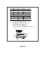
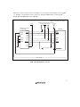
To our customers,
Old Company Name in Catalogs and Other Documents
On April 1st, 2010, NEC Electronics Corporation merged with Renesas Technology
Corporation, and Renesas Electronics Corporation took over all the business of both
companies. Therefore, although the old company name remains in this document, it is a valid
Renesas Electronics document. We appreciate your understanding.
Renesas Electronics website: http://www.renesas.com
April 1st, 2010
Renesas Electronics Corporation
Issued by: Renesas Electronics Corporation (http://www.renesas.com)
Send any inquiries to http://www.renesas.com/inquiry.
Notice
1.
2.
3.
4.
5.
6.
7.
All information included in this document is current as of the date this document is issued. Such information, however, is
subject to change without any prior notice. Before purchasing or using any Renesas Electronics products listed herein, please
confirm the latest product information with a Renesas Electronics sales office. Also, please pay regular and careful attention to
additional and different information to be disclosed by Renesas Electronics such as that disclosed through our website.
Renesas Electronics does not assume any liability for infringement of patents, copyrights, or other intellectual property rights
of third parties by or arising from the use of Renesas Electronics products or technical information described in this document.
No license, express, implied or otherwise, is granted hereby under any patents, copyrights or other intellectual property rights
of Renesas Electronics or others.
You should not alter, modify, copy, or otherwise misappropriate any Renesas Electronics product, whether in whole or in part.
Descriptions of circuits, software and other related information in this document are provided only to illustrate the operation of
semiconductor products and application examples. You are fully responsible for the incorporation of these circuits, software,
and information in the design of your equipment. Renesas Electronics assumes no responsibility for any losses incurred by
you or third parties arising from the use of these circuits, software, or information.
When exporting the products or technology described in this document, you should comply with the applicable export control
laws and regulations and follow the procedures required by such laws and regulations. You should not use Renesas
Electronics products or the technology described in this document for any purpose relating to military applications or use by
the military, including but not limited to the development of weapons of mass destruction. Renesas Electronics products and
technology may not be used for or incorporated into any products or systems whose manufacture, use, or sale is prohibited
under any applicable domestic or foreign laws or regulations.
Renesas Electronics has used reasonable care in preparing the information included in this document, but Renesas Electronics
does not warrant that such information is error free. Renesas Electronics assumes no liability whatsoever for any damages
incurred by you resulting from errors in or omissions from the information included herein.
Renesas Electronics products are classified according to the following three quality grades: “Standard”, “High Quality”, and
“Specific”. The recommended applications for each Renesas Electronics product depends on the product’s quality grade, as
indicated below. You must check the quality grade of each Renesas Electronics product before using it in a particular
application. You may not use any Renesas Electronics product for any application categorized as “Specific” without the prior
written consent of Renesas Electronics. Further, you may not use any Renesas Electronics product for any application for
which it is not intended without the prior written consent of Renesas Electronics. Renesas Electronics shall not be in any way
liable for any damages or losses incurred by you or third parties arising from the use of any Renesas Electronics product for an
application categorized as “Specific” or for which the product is not intended where you have failed to obtain the prior written
consent of Renesas Electronics. The quality grade of each Renesas Electronics product is “Standard” unless otherwise
expressly specified in a Renesas Electronics data sheets or data books, etc.
“Standard”:
8.
9.
10.
11.
12.
Computers; office equipment; communications equipment; test and measurement equipment; audio and visual
equipment; home electronic appliances; machine tools; personal electronic equipment; and industrial robots.
“High Quality”: Transportation equipment (automobiles, trains, ships, etc.); traffic control systems; anti-disaster systems; anticrime systems; safety equipment; and medical equipment not specifically designed for life support.
“Specific”:
Aircraft; aerospace equipment; submersible repeaters; nuclear reactor control systems; medical equipment or
systems for life support (e.g. artificial life support devices or systems), surgical implantations, or healthcare
intervention (e.g. excision, etc.), and any other applications or purposes that pose a direct threat to human life.
You should use the Renesas Electronics products described in this document within the range specified by Renesas Electronics,
especially with respect to the maximum rating, operating supply voltage range, movement power voltage range, heat radiation
characteristics, installation and other product characteristics. Renesas Electronics shall have no liability for malfunctions or
damages arising out of the use of Renesas Electronics products beyond such specified ranges.
Although Renesas Electronics endeavors to improve the quality and reliability of its products, semiconductor products have
specific characteristics such as the occurrence of failure at a certain rate and malfunctions under certain use conditions. Further,
Renesas Electronics products are not subject to radiation resistance design. Please be sure to implement safety measures to
guard them against the possibility of physical injury, and injury or damage caused by fire in the event of the failure of a
Renesas Electronics product, such as safety design for hardware and software including but not limited to redundancy, fire
control and malfunction prevention, appropriate treatment for aging degradation or any other appropriate measures. Because
the evaluation of microcomputer software alone is very difficult, please evaluate the safety of the final products or system
manufactured by you.
Please contact a Renesas Electronics sales office for details as to environmental matters such as the environmental
compatibility of each Renesas Electronics product. Please use Renesas Electronics products in compliance with all applicable
laws and regulations that regulate the inclusion or use of controlled substances, including without limitation, the EU RoHS
Directive. Renesas Electronics assumes no liability for damages or losses occurring as a result of your noncompliance with
applicable laws and regulations.
This document may not be reproduced or duplicated, in any form, in whole or in part, without prior written consent of Renesas
Electronics.
Please contact a Renesas Electronics sales office if you have any questions regarding the information contained in this
document or Renesas Electronics products, or if you have any other inquiries.
(Note 1) “Renesas Electronics” as used in this document means Renesas Electronics Corporation and also includes its majorityowned subsidiaries.
(Note 2) “Renesas Electronics product(s)” means any product developed or manufactured by or for Renesas Electronics.
User’s Manual
SuperH™ Family E10A-USB Emulator
Additional Document for User’s Manual
Supplementary Information
on Using the SH7606
Renesas Microcomputer Development
Environment System
SuperH™ Family / SH7600 Series
E10A-USB for SH7606 HS7606KCU01HE
Rev.1.00 2005.11
Keep safety first in your circuit designs!
1. Renesas Technology Corp. puts the maximum effort into making semiconductor products better and
more reliable, but there is always the possibility that trouble may occur with them. Trouble with
semiconductors may lead to personal injury, fire or property damage.
Remember to give due consideration to safety when making your circuit designs, with appropriate
measures such as (i) placement of substitutive, auxiliary circuits, (ii) use of nonflammable material or
(iii) prevention against any malfunction or mishap.
Notes regarding these materials
1. These materials are intended as a reference to assist our customers in the selection of the Renesas
Technology Corp. product best suited to the customer's application; they do not convey any license
under any intellectual property rights, or any other rights, belonging to Renesas Technology Corp. or
a third party.
2. Renesas Technology Corp. assumes no responsibility for any damage, or infringement of any thirdparty's rights, originating in the use of any product data, diagrams, charts, programs, algorithms, or
circuit application examples contained in these materials.
3. All information contained in these materials, including product data, diagrams, charts, programs and
algorithms represents information on products at the time of publication of these materials, and are
subject to change by Renesas Technology Corp. without notice due to product improvements or
other reasons. It is therefore recommended that customers contact Renesas Technology Corp. or
an authorized Renesas Technology Corp. product distributor for the latest product information
before purchasing a product listed herein.
The information described here may contain technical inaccuracies or typographical errors.
Renesas Technology Corp. assumes no responsibility for any damage, liability, or other loss rising
from these inaccuracies or errors.
Please also pay attention to information published by Renesas Technology Corp. by various means,
including the Renesas Technology Corp. Semiconductor home page (http://www.renesas.com).
4. When using any or all of the information contained in these materials, including product data,
diagrams, charts, programs, and algorithms, please be sure to evaluate all information as a total
system before making a final decision on the applicability of the information and products. Renesas
Technology Corp. assumes no responsibility for any damage, liability or other loss resulting from the
information contained herein.
5. Renesas Technology Corp. semiconductors are not designed or manufactured for use in a device or
system that is used under circumstances in which human life is potentially at stake. Please contact
Renesas Technology Corp. or an authorized Renesas Technology Corp. product distributor when
considering the use of a product contained herein for any specific purposes, such as apparatus or
systems for transportation, vehicular, medical, aerospace, nuclear, or undersea repeater use.
6. The prior written approval of Renesas Technology Corp. is necessary to reprint or reproduce in
whole or in part these materials.
7. If these products or technologies are subject to the Japanese export control restrictions, they must
be exported under a license from the Japanese government and cannot be imported into a country
other than the approved destination.
Any diversion or reexport contrary to the export control laws and regulations of Japan and/or the
country of destination is prohibited.
8. Please contact Renesas Technology Corp. for further details on these materials or the products
contained therein.
Contents
Section 1 Connecting the Emulator with the User System ................................1
1.1
1.2
1.3
1.4
1.5
Components of the Emulator ............................................................................................ 1
Connecting the E10A-USB Emulator with the User System ............................................ 2
Installing the H-UDI Port Connector on the User System ................................................ 2
Pin Assignments of the H-UDI Port Connector ................................................................ 2
Recommended Circuit between the H-UDI Port Connector and the MPU....................... 4
1.5.1 Recommended Circuit ......................................................................................... 4
Section 2 Specifications of the Software when Using the SH7606 ...................7
2.1
2.2
Differences between the SH7606 and the Emulator ......................................................... 7
Specific Functions for the Emulator when Using the SH7606.......................................... 10
2.2.1 Break Condition Functions .................................................................................. 11
2.2.2 Trace Functions.................................................................................................... 12
2.2.3 Note on Using the JTAG Clock (TCK) ............................................................... 13
2.2.4 Notes on Setting the [Breakpoint] Dialog Box .................................................... 13
2.2.5 Notes on Setting the [Break Condition] Dialog Box and
BREAKCONDITION_SET Command ............................................................... 14
2.2.6 Note on Setting the UBC_MODE Command ...................................................... 14
i
ii
Section 1 Connecting the Emulator with the User System
1.1
Components of the Emulator
The E10A-USB emulator supports the SH7606. Table 1.1 lists the components of the emulator.
Table 1.1 Components of the Emulator
Classification Component
Hardware
Appearance
Quantity
Emulator box
1
User system interface
cable
USB cable
1
1
Remarks
HS0005KCU01H:
Depth: 65.0 mm, Width: 97.0 mm,
Height: 20.0 mm, Mass: 72.9 g
or
HS0005KCU02H:
Depth: 65.0 mm, Width: 97.0 mm,
Height: 20.0 mm, Mass: 73.7 g
14-pin type:
Length: 20 cm, Mass: 33.1 g
Length: 150 cm, Mass: 50.6 g
Software
E10A-USB emulator
1
HS0005KCU01SR,
setup program,
TM
SuperH Family
HS0005KCU01HJ,
E10A-USB Emulator
HS0005KCU01HE,
User’s Manual,
Supplementary
HS7606KCU01HJ,
Information on Using
HS7606KCU01HE,
the SH7606*, and
Test program manual
HS0005TM01HJ, and
for HS0005KCU01H
HS0005TM01HE
and HS0005KCU02H
(provided on a CD-R)
Note: Additional document for the MPUs supported by the emulator is included. Check the target
MPU and refer to its additional document.
1
1.2
Connecting the E10A-USB Emulator with the User System
To connect the E10A-USB emulator (hereinafter referred to as the emulator), the H-UDI port
connector must be installed on the user system to connect the user system interface cable. When
designing the user system, refer to the recommended circuit between the H-UDI port connector
and the MCU. In addition, read the E10A-USB emulator user's manual and hardware manual for
the related device.
Table 1.2 shows the type number of the emulator, the corresponding connector type, and the use of
AUD function.
Table 1.2 Type Number, AUD Function, and Connector Type
Type Number
Connector
AUD Function
HS0005KCU01H, HS0005KCU02H
14-pin connector
Not available
1.3
Installing the H-UDI Port Connector on the User System
Table 1.3 shows the recommended H-UDI port connectors for the emulator.
Table 1.3 Recommended H-UDI Port Connectors
Connector
Type Number
Manufacturer
Specifications
14-pin connector
2514-6002
Minnesota Mining &
Manufacturing Ltd.
14-pin straight type
Note: When designing the 14-pin connector layout on the user board, do not place any
components within 3 mm of the H-UDI port connector.
1.4
Pin Assignments of the H-UDI Port Connector
Figure 1.1 shows the pin assignments of the H-UDI port connector.
Note: Note that the pin number assignments of the H-UDI port connector shown on the
following page differ from those of the connector manufacturer.
2
Pin No.
1
Signal
TCK
2* 2
Input/
Output*1
Note
SH7606 Pin No.
Input
N10
/TRST
Input
M11
3
TDO
Output
N11
4
N.C.
5
TMS
Input
P11
6
TDI
Input
R11
7*2
/RES
Output
R12
8
N.C.
9*4
11
(GND)
UVCC
Output
10, 12, GND
and 13
Output
GND
14*3
Notes: 1. Input to or output from the user system.
2. The slash (/) means that the signal is active-low.
3. The emulator monitors the GND signal of the user system and
detects whether or not the user system is connected.
4. The /ASEMODE pin must be 0 when the emulator is connected
and 1 when the emulator is not connected, respectively.
(1) When the emulator is used: /ASEMODE = 0
(2) When the emulator is not used: /ASEMODE = 1
To allow the /ASEMODE pin to be GND by connecting the user system
interface cable, connect pin 9 directly to the /ASEMODE pin. Do not ground the pin.
Pin 1 mark
H-UDI port connector (top view)
25.0
23.0
6 x 2.54 = 15.24
(2.54)
H-UDI port connector
(top view)
Pin 8
Pin 1
Pin 14
Pin 7
0.45
Pin 1 mark
Unit: mm
Figure 1.1 Pin Assignments of the H-UDI Port Connector (14 Pins)
3
1.5
Recommended Circuit between the H-UDI Port Connector and the
MPU
1.5.1
Recommended Circuit
Figure 1.2 shows a recommended circuit for connection between the H-UDI port connector (14
pins) and the MPU when the emulator is in use.
Notes: 1. Do not connect anything to the N.C. pins of the H-UDI port connector.
4
2.
The /ASEMODE pin must be 0 when the emulator is connected and 1 when the
emulator is not connected, respectively.
(1) When the emulator is used: /ASEMODE = 0
(2) When the emulator is not used: /ASEMODE = 1
Figure 1.2 shows an example of a circuit that allows the /ASEMODE pin to be GND
(0) whenever the emulator is connected by using the user system interface cable.
When the /ASEMODE pin is changed by switches, etc., ground pin 9. Do not connect
this pin to the /ASEMODE pin.
3.
When a network resistance is used for pull-up, it may be affected by a noise. Separate
TCK from other resistances.
4.
The pattern between the H-UDI port connector and the MPU must be as short as
possible. Do not connect the signal lines to other components on the board.
5.
When the power supply of the user system is turned off, supplying VccQ of the user
system to the UVCC pin reduces the leakage current from the emulator to the user
system. A level shifter that is activated by the internal power supply or user power
supply (changed by the switch) is installed in the interface circuit of the emulator. If
the user power is supplied to the UVCC pin, the level shifter is not activated as long as
no user power is supplied. When the power supply of the user system is turned off, no
current flows from the user interface. The I/O voltage level of the user system
interface can be the same as that of the VccQ. To operate the emulator with low
voltage (lower than 3.3 V), the VccQ must be supplied to the UVCC pin. Make the
emulator’s switch settings so that the VccQ will be supplied (SW2 = 1 and SW3 = 1)
(as shown in figure 1.2).
6.
The resistance value shown in figure 1.2 is recommended.
7.
For the pin processing in cases where the emulator is not used, refer to the hardware
manual of the related MPU.
When the circuit is connected as shown in figure 1.2, the switches of the emulator are set as SW2
TM
= 1 and SW3 = 1. For details, refer to section 3.8, Setting the DIP Switches, in the SuperH
Family E10A-USB Emulator User’s Manual.
VccQ = 3.3 V (I/O power supply)
VccQ
Pulled-up at 4.7 kΩ or more (all)
VccQ
VccQ VccQ VccQ
H-UDI port connector
(14-pin type)
TCK
9
(GND)
10 GND
TRST
TDO
SH7606
1
TCK
2
TRST
3
TDO
N.C. 4
12
13
GND
TMS
GND
TDI
14 GND
RESET
N.C.
UVCC
5
TMS
6
TDI
7
RES
1 kΩ
8
11
Reset signal
ASEMODE
User system
Figure 1.2 Recommended Circuit for Connection between the H-UDI Port Connector and
MPU when the Emulator is in Use
5
6
Section 2 Specifications of the Software when Using the
SH7606
2.1
Differences between the SH7606 and the Emulator
1. When the emulator system is initiated, it initializes the general registers and part of the control
registers as shown in table 2.1. The initial values of the actual SH7606 registers are undefined.
When the emulator is initiated from the workspace, a value to be entered is saved in a session.
Table 2.1 Register Initial Values at Emulator Link Up
Register
Emulator at Link Up
R0 to R14
H'00000000
R15 (SP)
SP in the vector address
PC
PC in the vector address
SR
H'000000F0
GBR
H'00000000
VBR
H'00000000
MACH
H'00000000
MACL
H'00000000
PR
H'00000000
2. The emulator uses the H-UDI; do not access the H-UDI.
3. Low-Power States (Sleep and Standby)
For low-power consumption, the SH7606 has sleep and standby states.
The sleep and standby states are switched using the SLEEP instruction. When the emulator is
used, only the sleep state can be cleared with either the normal clearing function or with the
[STOP] button, and a break will occur.
Note: The memory must not be accessed or modified in sleep state.
4. Reset Signals
The SH7606 reset signals are only valid during emulation started with clicking the GO or
STEP-type button. If these signals are input from the user system in command input wait state,
they are not sent to the SH7606.
Note: Do not break the user program when the /RES or /WAIT signal is being low. A
TIMEOUT error will occur. If the /WAIT signal is fixed to low during break, a
TIMEOUT error will occur at memory access.
7
5. Memory Access during User Program Execution
When a memory is accessed from the memory window, etc. during user program execution,
the user program is resumed after it has stopped in the emulator to access the memory.
Therefore, realtime emulation cannot be performed.
The stopping time of the user program is as follows:
Environment:
®
Host computer: 650 MHz (Pentium III)
®
OS: Windows 2000
JTAG clock: 5 MHz (TCK clock)
When a one-byte memory is read from the command-line window, the stopping time will be
about 40 ms.
6. Memory Access during User Program Break
The emulator can download the program for the flash memory area (refer to section 6.22,
TM
Download Function to the Flash Memory Area, in the SuperH Family E10A-USB Emulator
User’s Manual). Other memory write operations are enabled for the RAM area. Therefore, an
operation such as memory write or BREAKPOINT should be set only for the RAM area.
7. Cache Operation during User Program Break
When cache is enabled, the emulator accesses the memory by the following methods:
At memory write: Writes through the cache, then writes to the memory.
At memory read: Does not change the cache write mode that has been set.
Therefore, when memory read or write is performed during user program break, the cache state
will be changed.
8. UBC
When [User] is specified in the [UBC mode] list box in the [Configuration] dialog box, the
UBC can be used in the user program.
Do not use the UBC in the user program as it is used by the emulator when [EML] is specified
in the [UBC mode] list box of the [Configuration] dialog box.
9. Loading Sessions
Information in [JTAG clock] of the [Configuration] dialog box cannot be recovered by loading
sessions. Thus the TCK value will be 2.5 MHz.
10. [IO] Window
•
Display and modification
Do not change values of the User Break Controller because it is used by the emulator.
For each Watchdog Timer register, there are two registers to be separately used for write
and read operations.
8
Table 2.2 Watchdog Timer Register
Register Name
Usage
Register
WTCSR(W)
Write
Watchdog timer control/status register
WTCNT(W)
Write
Watchdog timer counter
WTCSR(R)
Read
Watchdog timer control/status register
WTCNT(R)
Read
Watchdog timer counter
•
The watchdog timer operates only when the user program is executed. Do not change the
value of the frequency change register in the [IO] window or [Memory] window.
•
The internal I/O registers can be accessed from the [IO] window. After the I/O-register
definition file is created, the MPU’s specification may be changed. If each I/O register in
the I/O-register definition file differs from addresses described in the hardware manual,
change the I/O-register definition file according to the description in the hardware manual.
The I/O-register definition file can be customized depending on its format. Note that,
however, the emulator does not support the bit-field function.
•
Verify
In the [IO] window, the verify function of the input value is disabled.
11. Illegal Instructions
If illegal instructions are executed by STEP-type commands, the emulator cannot go to the
next program counter.
9
2.2
Specific Functions for the Emulator when Using the SH7606
The SH7606 does not support the following functions:
• MMU-related functions (The SH7606 does not mount the MMU.)
⎯ VPMAP-related command
⎯ Virtual and Physical specification in the [Configuration] window
⎯ Virtual and Physical specification on the command-line function
⎯ Virtual and Physical specification in the [Breakpoint] window
⎯ LDTLB instruction execution break function
⎯ MEMORYAREA_SET command
• Profiler function
• Performance measurement function
• AUD trace function
10
2.2.1
Break Condition Functions
In the emulator, three break conditions can be set (Break Condition 1,2,3). Table 2.3 lists the
items that can be specified for each.
Table 2.3 Types of Break Conditions
Break Condition Type
Description
Address bus condition (Address)
Breaks when the SH7606 address bus value or the program
counter value matches the specified value.
Data bus condition (Data)
Breaks when the SH7606 data bus value matches the
specified value. Byte, word, or longword can be specified as
the access data size.
Bus state condition
(Bus State)
There are two bus state condition settings:
Read/Write condition: Breaks when the SH7606 RD or
RDWR signal level matches the specified condition.
Bus state condition: Breaks when the operating state in an
SH7606 bus cycle matches the specified condition.
Types of buses that can be specified are listed below.
•
L-bus (CPU-ALL): Indicates an instruction fetch and data
access, including a hit to the cache memory.
•
L-bus (CPU-Data): Indicates a data access by the CPU,
including a hit to the cache memory.
•
I-bus (CPU.DMA): Indicates a CPU cycle when the
cache memory is not hit, and a data access by the
DMA.
Internal I/O break condition
Breaks when the SH7606 accesses the internal I/O.
Count
Breaks when the conditions set are satisfied the specified
number of times.
Note: When U-RAM is accessed from the P0 space, the I-bus must be selected, and when
accessed from the P2 space, the L-bus must be selected. When cache fill cycle is acquired,
the I-bus must be selected.
11
Table 2.4 lists the combinations of conditions that can be set under Break Condition 1,2,3.
Table 2.4 Dialog Boxes for Setting Break Conditions
Type
Dialog Box
Address Bus
Condition
(Address)
Data Bus
Condition
(Data)
Bus State
Condition
(Bus Status)
Count
Condition
(Count)
Internal
I/O Break
[Break Condition 1]
dialog box
O
O
O
O
X
[Break Condition 2]
dialog box
O
X
O
X
X
[Break Condition 3]
dialog box
X
X
X
X
O
Note: O: Can be set in the dialog box.
X: Cannot be set in the dialog box.
2.2.2
Trace Functions
When the SH7606 is used, the trace functions listed in table 2.5 can be used.
Table 2.5 Trace Functions
Function
Internal Trace
Branch trace
Supported (four branches)
Range memory access trace
Not supported
Software trace
Not supported
Internal Trace Function: This function is activated by selecting the [Internal trace] radio button
in the [Trace type] group box of the [Trace mode] page. This function traces and displays the
branch instructions. The branch source address and branch destination address for the four latest
branch instructions are displayed.
Notes: 1. If an interrupt is generated at the program execution start or end, including a step
execution, the emulator address may be acquired. In such a case, the following
message will be displayed. Ignore this address because it is not a user program
address.
*** EML ***
2. If a completion-type exception occurs during exception branch acquisition, the next
address to the address in which an exception occurs is acquired.
12
3. Trace information cannot be acquired for the following branch instructions:
• The BF and BT instructions whose displacement value is 0
• Branch to H'A0000000 by reset
2.2.3
4.
When [User] is specified in the [UBC mode] list box in the [Configuration] window,
the internal trace is not acquired. In this case, exit the [Trace] window.
5.
When the SH7606 is used, the source code cannot be displayed on the [Trace]
window.
Note on Using the JTAG Clock (TCK)
Set the JTAG clock (TCK) frequency to lower than the frequency of the SH7606 peripheral
module clock (CKP).
The set value of the JTAG clock (TCK) is initialized by executing [Reset CPU] or [Reset Go].
2.2.4
Notes on Setting the [Breakpoint] Dialog Box
1. When an odd address is set, the next lowest even address is used.
2. A BREAKPOINT is accomplished by replacing instructions of the specified address.
Accordingly, it can be set only to the RAM areas in CS0 to CS6 and the internal RAM areas.
However, a BREAKPOINT cannot be set to the following addresses:
• ROM areas in CS0 to CS6
• Areas other than the internal RAM
• Areas other than CS0 to CS6
• A slot instruction of a delayed branch instruction
3. During step operation, BREAKPOINTs are disabled.
4. Conditions set at Break Condition 2 are disabled when an instruction to which a
BREAKPOINT has been set is executed. Do not set a BREAKPOINT to an instruction in
which Break Condition 2 is satisfied.
5. When execution resumes from the address where a BREAKPOINT is specified, single-step
operation is performed at the address and execution is continued from the next PC value.
Therefore, realtime operation cannot be performed.
6. When a BREAKPOINT is set to the slot instruction of a delayed branch instruction, the PC
value becomes an illegal value. Accordingly, do not set a BREAKPOINT to the slot
instruction of a delayed branch instruction.
7. When a BREAKPOINT is set to the cacheable area, the cache block containing the
BREAKPOINT address is filled immediately before and after user program execution.
13
8. If an address of a BREAKPOINT cannot be correctly set in the ROM or flash memory area, a
mark z will be displayed in the [BP] area of the address on the [Editor] or [Disassembly]
window by refreshing the [Memory] window, etc. after Go execution. However, no break will
occur at this address. When the program halts with the break condition, the mark z
disappears.
2.2.5
Notes on Setting the [Break Condition] Dialog Box and BREAKCONDITION_SET
Command
1. When [Go to cursor], [Step In], [Step Over], or [Step Out] is selected, the settings of Break
Condition 2 are disabled.
2.
Break Condition 2 is disabled when an instruction to which a BREAKPOINT has been set is
executed. Accordingly, do not set a BREAKPOINT to an instruction which satisfies Break
Condition 2.
3.
When a Break Condition is satisfied, emulation may stop after two or more instructions have
been executed.
4.
If a PC break address condition is set to the slot instruction after a delayed branch instruction,
user program execution cannot be terminated before the slot instruction execution; execution
stops before the branch destination instruction.
5.
Note that a break occurs with a break satisfaction condition by an instruction that has been
cancelled due to the generation of an exception.
6.
Use the sequential break or count break with the L-bus condition. If such break is used with
the I-bus condition, it will not operate correctly.
7.
A break will not occur with the execution counts specified on the execution of the multi-step
instruction.
2.2.6
Note on Setting the UBC_MODE Command
In the [Configuration] dialog box, if [User] is set while the [UBC mode] list box has been set, the
STEP-type commands that use Break Condition 2 for implementation cannot be used.
14
SuperH™ Family E10A-USB Emulator
Additional Document for User's Manual
Supplementary Information on Using the SH7606
Publication Date: Rev.1.00, November 2, 2005
Published by:
Sales Strategic Planning Div.
Renesas Technology Corp.
Edited by:
Customer Support Department
Global Strategic Communication Div.
Renesas Solutions Corp.
© 2005. Renesas Technology Corp., All rights reserved. Printed in Japan.
Sales Strategic Planning Div.
Nippon Bldg., 2-6-2, Ohte-machi, Chiyoda-ku, Tokyo 100-0004, Japan
RENESAS SALES OFFICES
http://www.renesas.com
Refer to "http://www.renesas.com/en/network" for the latest and detailed information.
Renesas Technology America, Inc.
450 Holger Way, San Jose, CA 95134-1368, U.S.A
Tel: <1> (408) 382-7500, Fax: <1> (408) 382-7501
Renesas Technology Europe Limited
Dukes Meadow, Millboard Road, Bourne End, Buckinghamshire, SL8 5FH, United Kingdom
Tel: <44> (1628) 585-100, Fax: <44> (1628) 585-900
Renesas Technology (Shanghai) Co., Ltd.
Unit2607 Ruijing Building, No.205 Maoming Road (S), Shanghai 200020, China
Tel: <86> (21) 6472-1001, Fax: <86> (21) 6415-2952
Renesas Technology Hong Kong Ltd.
7th Floor, North Tower, World Finance Centre, Harbour City, 1 Canton Road, Tsimshatsui, Kowloon, Hong Kong
Tel: <852> 2265-6688, Fax: <852> 2730-6071
Renesas Technology Taiwan Co., Ltd.
10th Floor, No.99, Fushing North Road, Taipei, Taiwan
Tel: <886> (2) 2715-2888, Fax: <886> (2) 2713-2999
Renesas Technology Singapore Pte. Ltd.
1 Harbour Front Avenue, #06-10, Keppel Bay Tower, Singapore 098632
Tel: <65> 6213-0200, Fax: <65> 6278-8001
Renesas Technology Korea Co., Ltd.
Kukje Center Bldg. 18th Fl., 191, 2-ka, Hangang-ro, Yongsan-ku, Seoul 140-702, Korea
Tel: <82> 2-796-3115, Fax: <82> 2-796-2145
Renesas Technology Malaysia Sdn. Bhd.
Unit 906, Block B, Menara Amcorp, Amcorp Trade Centre, No.18, Jalan Persiaran Barat, 46050 Petaling Jaya, Selangor Darul Ehsan, Malaysia
Tel: <603> 7955-9390, Fax: <603> 7955-9510
Colophon 4.0
SuperH™ Family E10A-USB Emulator
Additional Document for User’s Manual
Supplementary Information
on Using the SH7606
1753, Shimonumabe, Nakahara-ku, Kawasaki-shi, Kanagawa 211-8668 Japan
REJ10J1145-0100