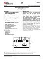
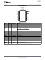
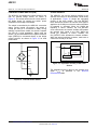
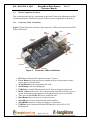
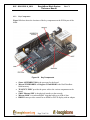
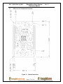
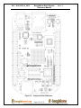
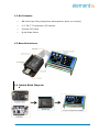
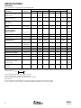
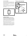
1
Anexo A – Especificaciones de los componentes del sistema final 1. Resumen Este documento es el Anexo A perteneciente al trabajo de final de grado, Diseño de un sistema de cobro automático para supermercados. En este anexo A, se encontrará la información sobre las especificaciones y datos técnicos de los componentes que forman el sistema de cobro automático diseñado. Se incluirán tanto los componentes integrados en el carro de la compra como los del puesto de cobro. Anexo A – Especificaciones de los componentes del sistema final 2. Sumario 1. Resumen 2. Sumario 3. Componentes integrados en el carro de la compra 3.1. Células de carga Senel SX-1 3.2. Convertidor ADS1231 3.3. Beaglebone Black 3.4. BB View Cape – LCD 7’’ 3.5. Módulo Bluetooth 3.6. Batería 3.7. BMS 3.8. REF-02 5V Precision Voltage 4. Componentes del puesto de cobro 4.1. Lector de tarjetas de crédito Hitachi-Omron V2BF 4.2. Fuente de alimentación 12V CP SNT 55W 4.3. Impresora de tickets térmica Epson TM-T20 4.4. Pantalla táctil MaxPos DTK-1598 4.5. Puertas automáticas PNG 390 y PNG 390 Twin 3.1. Células de carga Senel SX-1 3.2. Convertidor ADS1231 ADS1231 www.ti.com SBAS414D – JULY 2009 – REVISED OCTOBER 2013 24-Bit Analog-to-Digital Converter for Bridge Sensors Check for Samples: ADS1231 FEATURES DESCRIPTION • • • • • • • The ADS1231 is a precision, 24-bit analog-to-digital converter (ADC). With an onboard low-noise amplifier, onboard oscillator, precision third-order 24bit delta-sigma (ΔΣ) modulator, and bridge power switch, the ADS1231 provides a complete front-end solution for bridge sensor applications including weigh scales, strain gauges, and load cells. 1 2 • • • • • • • Complete Front-End for Bridge Sensors Internal Amplifier, Gain of 128 Internal Oscillator Low-Side Power Switch for Bridge Sensor Low Noise: 35nVrms Selectable Data Rates: 10SPS or 80SPS Simultaneous 50Hz and 60Hz Rejection at 10SPS Input EMI Filter External Voltage Reference up to 5V for Ratiometric Measurements Simple, Pin-Driven Control Two-Wire Serial Digital Interface Supply Range: 3V to 5.3V Package: SOIC-16 Temperature Range: –40°C to +85°C The low-noise amplifier has a gain of 128, supporting a full-scale differential input of ±19.5mV. The ΔΣ ADC has 24-bit resolution and is comprised of a third-order modulator and fourth-order digital filter. Two data rates are supported: 10SPS (with both 50Hz and 60Hz rejection) and 80SPS. The ADS1231 can be put in a low-power standby mode or shut off completely in power-down mode. The ADS1231 is controlled by dedicated pins; there are no digital registers to program. Data are output over an easily-isolated serial interface that connects directly to the MSP430 and other microcontrollers. The ADS1231 is available in an SO-16 package and is specified from –40°C to +85°C. APPLICATIONS • • • • Weigh Scales Strain Gauges Load Cells Industrial Process Control AVDD CAP CAP VREFP VREFN DVDD PDWN AINP AINN EMI Filter G = 128 24-Bit DS ADC Internal Oscillator DRDY/DOUT SCLK SPEED SW GND CLKIN 1 2 Please be aware that an important notice concerning availability, standard warranty, and use in critical applications of Texas Instruments semiconductor products and disclaimers thereto appears at the end of this data sheet. All trademarks are the property of their respective owners. PRODUCTION DATA information is current as of publication date. Products conform to specifications per the terms of the Texas Instruments standard warranty. Production processing does not necessarily include testing of all parameters. Copyright © 2009–2013, Texas Instruments Incorporated ADS1231 SBAS414D – JULY 2009 – REVISED OCTOBER 2013 www.ti.com This integrated circuit can be damaged by ESD. Texas Instruments recommends that all integrated circuits be handled with appropriate precautions. Failure to observe proper handling and installation procedures can cause damage. ESD damage can range from subtle performance degradation to complete device failure. Precision integrated circuits may be more susceptible to damage because very small parametric changes could cause the device not to meet its published specifications. ORDERING INFORMATION For the most current package and ordering information, see the Package Option Addendum at the end of this document, or visit the device product folder at www.ti.com. ABSOLUTE MAXIMUM RATINGS (1) Over operating free-air temperature range, unless otherwise noted. ADS1231 UNIT AVDD to GND –0.3 to +6 V DVDD to GND –0.3 to +6 V 100, momentary mA Input current 10, continuous mA Analog input voltage to GND –0.3 to AVDD + 0.3 V Digital input voltage to GND –0.3 to DVDD + 0.3 V Human body model (HBM) JEDEC standard 22, test method A114-C.01, all pins ±2000 V Charged device model (CDM) JEDEC standard 22, test method C101, all pins ±500 V ESD (2) Maximum junction temperature +150 °C Operating temperature range –40 to +85 °C Storage temperature range –60 to +150 °C (1) (2) Stresses beyond those listed under Absolute Maximum Ratings may cause permanent damage to the device. These are stress ratings only, and functional operation of the device at these or any other conditions beyond those indicated is not implied. Exposure to absolutemaximum-rated conditions for extended periods may affect device reliability. CAUTION: ESD sensitive device. Precaution should be used when handling the device in order to prevent permanent damage. THERMAL INFORMATION ADS1231 THERMAL METRIC (1) SOIC (D) UNITS 16 PINS θJA Junction-to-ambient thermal resistance 79.5 θJCtop Junction-to-case (top) thermal resistance 37.5 θJB Junction-to-board thermal resistance 37.1 ψJT Junction-to-top characterization parameter 5.6 ψJB Junction-to-board characterization parameter 36.7 θJCbot Junction-to-case (bottom) thermal resistance n/a (1) 2 °C/W For more information about traditional and new thermal metrics, see the IC Package Thermal Metrics application report, SPRA953. Submit Documentation Feedback Copyright © 2009–2013, Texas Instruments Incorporated Product Folder Links: ADS1231 ADS1231 www.ti.com SBAS414D – JULY 2009 – REVISED OCTOBER 2013 ELECTRICAL CHARACTERISTICS Minimum/maximum limit specifications apply from –40°C to +85°C. Typical specifications at +25°C. All specifications at AVDD = DVDD = VREFP = +5V, VCM = 2.5V and VREFN = GND, unless otherwise noted. ADS1231 PARAMETER CONDITIONS MIN TYP MAX UNIT ANALOG INPUTS Full-scale input voltage (AINP – AINN) ±0.5VREF / 128 V VREF = AVDD = 5V ±19.5 mV VREF = AVDD = 3V ±11.7 mV Common-mode input range GND + 1.5 Differential input current AVDD – 1.5 V ±2 nA LOW-SIDE POWER SWITCH On-resistance (RON) Ω AVDD = 5V, ISW = 30mA 3.5 5 AVDD = 3V, ISW = 30mA 4 7 Ω 30 mA Current through switch SYSTEM PERFORMANCE Resolution No missing codes 24 Internal oscillator, SPEED = high Data rate SPS Internal oscillator, SPEED = low 10 SPS External clock, SPEED = high fCLKIN / 61,440 SPS External clock, SPEED = low fCLKIN / 491,520 SPS Full settling 4 Conversions fDATA = 10SPS, AVDD = VREF = 5V 35 nV, rms fDATA = 80SPS, AVDD = VREF = 5V 102 nV, rms fDATA = 10SPS, AVDD = VREF = 5V 232 nV, P-P fDATA = 80SPS, AVDD = VREF = 5V 622 nV, P-P Differential input, end-point fit ±8 ppm Digital filter settling time Noise Integral nonlinearity (INL) Bits 80 Input offset error 10 μV Input offset drift ±20 nV/°C Gain error 1 % Gain drift ±2 ppm/°C Normal-mode rejection (1) fIN = 50Hz or 60Hz ±1Hz, fDATA = 10SPS, internal oscillator 80 100 dB fIN = 50Hz or 60Hz ±1Hz, fDATA = 10SPS, external clock (2) 90 110 dB Common-mode rejection At dc Power-supply rejection At dc 110 dB 90 100 dB 1.5 AVDD VOLTAGE REFERENCE INPUT Voltage reference input (VREF) AVDD + 0.1 V Negative reference input (VREFN) VREF = VREFP – VREFN GND – 0.1 VREFP – 1.5 V Positive reference input (VREFP) VREFN + 1.5 AVDD + 0.1 Voltage reference input current V 10 nA DIGITAL INPUT/OUTPUT (DVDD = 3V to 5.3V) Logic levels VIH 0.8 DVDD DVDD + 0.1 V VIL GND 0.2 DVDD V VOH IOH = 500μA VOL IOL = 500μA 0.2 DVDD V 0 < VDIGITAL INPUT < DVDD ±10 μA 6 MHz 5 MHz Input leakage DVDD – 0.4 External clock input frequency (fCLKIN) 1 Serial clock input frequency (fSCLK) (1) (2) V 4.9152 Specification is assured by the combination of design and final test. fCLKIN = 4.9152MHz. Submit Documentation Feedback Copyright © 2009–2013, Texas Instruments Incorporated Product Folder Links: ADS1231 3 ADS1231 SBAS414D – JULY 2009 – REVISED OCTOBER 2013 www.ti.com ELECTRICAL CHARACTERISTICS (continued) Minimum/maximum limit specifications apply from –40°C to +85°C. Typical specifications at +25°C. All specifications at AVDD = DVDD = VREFP = +5V, VCM = 2.5V and VREFN = GND, unless otherwise noted. ADS1231 PARAMETER CONDITIONS MIN TYP MAX UNIT POWER SUPPLY Power-supply voltage (AVDD, DVDD) 3 V 900 μA Normal mode, AVDD = 5V 900 μA Standby mode 0.1 μA Power-down 0.1 μA Normal mode, DVDD = 3V 60 μA Normal mode, DVDD = 5V 95 μA Standby mode, SCLK = high, DVDD = 3V 45 μA Standby mode, SCLK = high, DVDD = 5V 65 μA Power-down 0.2 μA Normal mode, AVDD = DVDD = 3V 2.9 mW Normal mode, AVDD = DVDD = 5V 5 mW Analog supply current Digital supply current 5.3 Normal mode, AVDD = 3V Power dissipation, total TEMPERATURE Operating temperature range –40 +85 °C Specified temperature range –40 +85 °C 4 Submit Documentation Feedback Copyright © 2009–2013, Texas Instruments Incorporated Product Folder Links: ADS1231 ADS1231 www.ti.com SBAS414D – JULY 2009 – REVISED OCTOBER 2013 PIN CONFIGURATION D PACKAGE SO-16 (TOP VIEW) DVDD 1 16 DRDY/DOUT GND 2 15 SCLK CLKIN 3 14 PDWN SPEED 4 13 AVDD CAP 5 12 SW CAP 6 11 GND AINP 7 10 VREFP AINN 8 9 VREFN PIN DESCRIPTIONS NAME TERMINAL ANALOG/DIGITAL INPUT/OUTPUT DVDD 1 Digital Digital power supply GND 2 Supply Ground for digital and analog supplies CLKIN 3 Digital input DESCRIPTION External clock input: typically 4.9152MHz. Tie low to activate internal oscillator. Data rate select: SPEED 4 CAP 5 CAP AINP Digital input SPEED DATA RATE 0 10SPS 1 80SPS Analog Gain amplifier bypass capacitor connection 6 Analog Gain amplifier bypass capacitor connection 7 Analog input Positive analog input AINN 8 Analog input Negative analog input VREFN 9 Analog input Negative reference input VREFP 10 Analog input Positive reference input GND 11 Supply Ground for digital and analog supplies SW 12 Analog Low-side power switch AVDD 13 Supply Analog power supply PDWN 14 Digital input Power-down: holding this pin low powers down the entire converter and resets the ADC. SCLK 15 Digital input Serial clock: clock out data on the rising edge. Also used to initiate Standby mode. See the Standby Mode section for more details. DRDY/DOUT 16 Digital output Dual-purpose output: Data ready: indicates valid data by going low. Data output: outputs data, MSB first, on the first rising edge of SCLK. Submit Documentation Feedback Copyright © 2009–2013, Texas Instruments Incorporated Product Folder Links: ADS1231 5 ADS1231 SBAS414D – JULY 2009 – REVISED OCTOBER 2013 www.ti.com NOISE PERFORMANCE The ADS1231 offers outstanding noise performance. Table 1 summarizes the typical noise performance with inputs shorted externally for different data rates and voltage reference values. The RMS and Peak-to-Peak noise are referred to the input. The effective number of bits (ENOB) is defined as: ENOB = ln (FSR/RMS noise)/ln(2) The Noise-Free Bits are defined as: Noise-Free Bits = ln (FSR/Peak-to-Peak Noise)/ln(2) Where: FSR (Full-Scale Range) = VREF/Gain. Table 1. Noise Performance DATA RATE 10 80 (1) 6 AVDD and VREF (V) RMS NOISE (1) (nV) PEAK-TO-PEAK NOISE (1) (nV) ENOB (RMS) NOISE-FREE BITS 5 35.2 231.9 20.1 17.4 3 33.5 199.2 19.4 16.8 5 102.1 622.1 18.5 15.9 3 80.3 549.6 18.2 15.4 Noise specifications are based on direct measurement of 1024 consecutive samples. Submit Documentation Feedback Copyright © 2009–2013, Texas Instruments Incorporated Product Folder Links: ADS1231 ADS1231 www.ti.com SBAS414D – JULY 2009 – REVISED OCTOBER 2013 TYPICAL CHARACTERISTICS At TA = +25°C, AVDD = DVDD = REFP = 5V, REFN = GND, and VCM = 2.5V unless otherwise noted. NOISE vs TIME NOISE vs TIME 300 300 Data Rate = 10SPS 200 200 150 150 100 50 0 −50 −100 −150 100 50 0 −50 −100 −150 −200 −200 −250 −250 −300 0 200 Data Rate = 80SPS 250 Conversion Data (nV) Conversion Data (nV) 250 400 600 Time (Reading Number) 800 −300 1000 0 200 400 600 Time (Reading Number) Figure 1. NOISE HISTOGRAM NOISE HISTOGRAM 250 Data Rate = 10SPS Data Rate = 80SPS 225 400 200 350 175 # of Occurrences # of Occurrences 450 300 250 200 150 150 125 100 75 100 50 50 25 0 −40−35−30−25−20−15−10 −5 0 5 10 15 20 25 30 35 40 24−bit LSBs −40−35−30−25−20−15−10 −5 0 5 10 15 20 25 30 35 40 24−bit LSBs Figure 3. Figure 4. NOISE vs INPUT VOLTAGE NOISE vs INPUT VOLTAGE 150 150 Data Rate = 10SPS Data Rate = 80SPS 125 RMS Noise (nV) 125 RMS Noise (nV) 1000 Figure 2. 500 0 800 100 75 50 25 0 −20 100 75 50 25 −15 −10 −5 0 5 Input Voltage (mV) 10 15 20 0 −20 Figure 5. −15 −10 −5 0 5 Input Voltage (mV) 10 15 20 Figure 6. Submit Documentation Feedback Copyright © 2009–2013, Texas Instruments Incorporated Product Folder Links: ADS1231 7 ADS1231 SBAS414D – JULY 2009 – REVISED OCTOBER 2013 www.ti.com TYPICAL CHARACTERISTICS (continued) At TA = +25°C, AVDD = DVDD = REFP = 5V, REFN = GND, and VCM = 2.5V unless otherwise noted. GAIN ERROR vs TEMPERATURE 0.02 1500 0.015 1000 0.01 Gain Error (%) Offset (nV) OFFSET DRIFT vs TEMPERATURE 2000 500 0 -500 0.005 0 -0.005 -1000 -0.01 -1500 -0.015 -2000 -0.02 10 -40 -27.5 -15 -2.5 22.5 35 47.5 60 85 72.5 -40 -27.5 -15 -2.5 22.5 47.5 35 Temperature (°C) Figure 7. Figure 8. INL vs INPUT VOLTAGE 3 60 72.5 85 72.5 85 DATA RATE vs TEMPERATURE -20°C -40°C 2 10.2 +25°C +70°C Data Rate = 10SPS 10.15 1 10.1 0 Data Rate (SPS) Integral Nonlinearity (ppm) 10 Temperature (°C) -1 -2 -3 -4 10.05 10 9.95 -5 9.9 -6 9.85 -7 -20 -15 0 -5 -10 5 10 15 20 9.8 −40 −27.5 −15 −2.5 Input Voltage (mV) Figure 9. ANALOG SUPPLY CURRENT vs TEMPERATURE DIGITAL SUPPLY CURRENT vs TEMPERATURE 120 115 1000 Digital Supply Current (mA) Analog Supply Current (mA) 60 Figure 10. 1200 800 600 400 200 110 105 100 95 90 85 0 80 -40 -27.5 -15 -2.5 10 22.5 35 47.5 60 72.5 85 -40 -27.5 -15 -2.5 Temperature (°C) 10 22.5 35 47.5 60 72.5 85 Temperature (°C) Figure 11. 8 10 22.5 35 47.5 Temperature (°C) Figure 12. Submit Documentation Feedback Copyright © 2009–2013, Texas Instruments Incorporated Product Folder Links: ADS1231 ADS1231 www.ti.com SBAS414D – JULY 2009 – REVISED OCTOBER 2013 OVERVIEW The ADS1231 is a precision, 24-bit ADC that includes a low-noise PGA, internal oscillator, third-order deltasigma (ΔΣ) modulator, and fourth-order digital filter. The ADS1231 provides a complete front-end solution for bridge sensor applications such as weigh scales, strain gauges, and pressure sensors. Data can be output at 10SPS for excellent 50Hz and 60Hz rejection, or at 80SPS when higher speeds are needed. The ADS1231 is easy to configure, and all digital control is accomplished through dedicated pins; there are no registers to program. A simple twowire serial interface retrieves the data. ANALOG INPUTS (AINP, AINN) The input signal to be measured is applied to the input pins AINP and AINN. The ADS1231 accepts differential input signals, but can also measure unipolar signals. LOW-NOISE AMPLIFIER The ADS1231 features a low-drift, low-noise amplifier that provides a complete front-end solution for bridge sensors. A simplified diagram of the amplifier is shown in Figure 13. It consists of two chopperstabilized amplifiers (A1 and A2) and three accurately matched resistors (R1, RF1, and RF2) that construct a differential front-end stage with a gain of 128, followed by gain stage A3 (Gain = 1). The inputs are equipped with an EMI filter, as shown in Figure 13. The cutoff frequency of the EMI filter is 20MHz. By using AVDD as the reference input, the bipolar input ranges from –19.5mV to +19.5mV. The inputs of the ADS1231 are protected with internal diodes connected to the power-supply rails. These diodes clamp the applied signal to prevent it from damaging the input circuitry. External Capacitor An external capacitor (CEXT) across the two ADS1231 CAP pins combines with the internal resistor RINT (onchip) to create a low-pass filter. The recommended value for CEXT is 0.1μF which provides a corner frequency of 720Hz. This low-pass filter serves two purposes. First, the input signal is band-limited to prevent aliasing by the ADC and to filter out the highfrequency noise. Second, it attenuates the chopping residue from the amplifier to improve temperature drift performance. NPO or C0G capacitors are recommended. For optimal performance, place the external capacitor very close to the CAP pins. VOLTAGE REFERENCE INPUTS (VREFP, VREFN) The voltage reference used by the modulator is generated from the voltage difference between VREFP and VREFN: VREF = VREFP – VREFN. The reference inputs use a structure similar to that of the analog inputs. In order to increase the reference input impedance, switching buffer circuitry is used to reduce the input equivalent capacitance. The reference drift and noise impact ADC performance. In order to achieve best results, pay close attention to the reference noise and drift specifications. A simplified diagram of the circuitry on the reference inputs is shown in Figure 14. The switches and capacitors can be modeled approximately using an effective impedance of ZEFF = 500MW. VREFP VREFN AVDD AVDD CAP ESD Protection AINP EMI Filter RINT CBUF A1 R Gain = 1 F1 R1 A3 RF2 ADC Figure 14. Simplified Reference Input Circuitry RINT ESD diodes protect the reference inputs. To prevent these diodes from turning on, make sure the voltages on the reference pins do not go below GND by more than 100mV, and likewise, do not exceed AVDD by 100mV: A2 AINN ZEFF = 500MW EMI Filter CAP Figure 13. Simplified Diagram of the Amplifier GND – 100mV < (VREFP or VREFN) < AVDD + 100mV Submit Documentation Feedback Copyright © 2009–2013, Texas Instruments Incorporated Product Folder Links: ADS1231 9 ADS1231 SBAS414D – JULY 2009 – REVISED OCTOBER 2013 www.ti.com LOW-SIDE POWER SWITCH (SW) CLOCK SOURCE The ADS1231 incorporates an internal switch for use with an external bridge sensor, as shown in Figure 15. The switch can be used in a return path for the bridge power. By opening the switch, power dissipation in the bridge is eliminated. The ADS1231 can use the internal oscillator or an external clock source to accommodate a wide variety of applications. Figure 16 shows the equivalent circuitry of the clock module. The CLK_DETECT block determines whether an external clock signal is applied to the CLKIN pin so that the internal oscillator is bypassed or activated. When the CLKIN pin frequency is above ~200kHz, the CLK_DETECT circuit shuts down the internal oscillator and passes the external clock signal to the ADC. When the CLKIN pin frequency is below ~200kHz, the CLK_DETECT block activates the internal oscillator. When the internal oscillator is chosen, make sure to connect the CLKIN pin to GND. The switch is controlled by the ADS1231 conversion status. During normal conversions, the switch is closed (the SW pin is connected to GND). During standby or power-down modes, the switch is opened (the SW pin is high impedance). When using the switch, it is recommended that the negative reference input (VREFN) be connected directly to the bridge ground terminal, as shown in Figure 15 for best performance. +VDD CLKIN ADS1231 CLK_DETECT Internal Oscillator VREFP S0 Bridge Sensor S1 MUX AINP EN S To ADC AINN Figure 16. Equivalent Circuitry of the Clock Source VREFN SW The allowable frequency range for the external clock signal fCLKIN is specified in the Electrical Characteristics table. GND Figure 15. Low-Side Power Switch 10 Submit Documentation Feedback Copyright © 2009–2013, Texas Instruments Incorporated Product Folder Links: ADS1231 ADS1231 www.ti.com SBAS414D – JULY 2009 – REVISED OCTOBER 2013 FREQUENCY RESPONSE 0 Data Rate = 10SPS 4 -50 Gain (dB) The ADS1231 uses a sinc digital filter with the frequency response shown in Figure 17 for fCLKIN = 4.9152MHz. The frequency response repeats at multiples of the modulator sampling frequency of 76.8kHz. The overall response is that of a low-pass filter with a –3dB cutoff frequency of 3.32Hz with the SPEED pin tied low (10SPS data rate) and 11.64Hz with the SPEED pin tied high (80SPS data rate). -100 To help see the response at lower frequencies, Figure 17(a) illustrates the nominal response out to 100Hz, when the data rate = 10SPS. Notice that signals at multiples of 10Hz are rejected, and therefore simultaneous rejection of 50Hz and 60Hz is achieved. -150 0 30 40 50 60 70 80 90 100 (a) -50 Data Rate = 10SPS Gain (dB) The ADS1231 data rate and frequency response scale directly with clock frequency. For example, if fCLKIN increases from 4.9152MHz to 5.5296MHz when the SPEED pin is tied high, the data rate increases from 80SPS to 90SPS, while the notch also increases from 80Hz to 90Hz. Note that these changes are only possible when an external clock source is applied. 20 Frequency (Hz) The benefit of using a sinc4 filter is that every frequency notch has four zeros on the same location, thus providing excellent normal-mode rejection of line-cycle interference. Figure 17(b) zooms in on the 50Hz and 60Hz notches with the SPEED pin tied low (10SPS data rate). 10 -100 -150 46 47 48 49 50 51 52 53 54 55 56 57 58 59 60 61 62 63 64 Frequency (Hz) (b) Figure 17. Nominal Frequency Response Out To 100Hz Submit Documentation Feedback Copyright © 2009–2013, Texas Instruments Incorporated Product Folder Links: ADS1231 11 ADS1231 SBAS414D – JULY 2009 – REVISED OCTOBER 2013 www.ti.com Table 2. Data Rate Settings SETTLING TIME Fast changes in the input signal require time to settle. For example, an external multiplexer in front of the ADS1231 can generate abrupt changes in input voltage by simply switching the multiplexer input channels. These sorts of changes in the input require four data conversion cycles to settle. When continuously converting, five readings may be necessary in order to settle the data. If the change in input occurs in the middle of the first conversion, four more full conversions of the fully-settled input are required to obtain fully-settled data. Discard the first four readings because they contain only partiallysettled data. Figure 18 illustrates the settling time for the ADS1231. DATA RATE SPEED PIN Internal Oscillator External Clock 0 10SPS fCLKIN / 491,520 1 80SPS fCLKIN / 61,440 DATA FORMAT The ADS1231 outputs 24 bits of data in binary twos complement format. The least significant bit (LSB) has a weight of (0.5VREF/128)(223 – 1). The positive full-scale input produces an output code of 7FFFFFh and the negative full-scale input produces an output code of 800000h. The output clips at these codes for signals exceeding full-scale. Table 3 summarizes the ideal output codes for different input signals. DATA RATE Table 3. Ideal Output Code vs Input Signal The ADS1231 data rate is set by the SPEED pin, as shown in Table 2. When SPEED is low, the data rate is nominally 10SPS. This data rate provides the lowest noise, and also has excellent rejection of both 50Hz and 60Hz line-cycle interference. For applications requiring fast data rates, setting SPEED high selects a data rate of nominally 80SPS. INPUT SIGNAL VIN (AINP – AINN) IDEAL OUTPUT ≥ +0.5VREF/128 7FFFFFh (+0.5VREF/128)/(223 – 1) 000001h 0 000000h (–0.5VREF/128)/(223 – 1) FFFFFFh ≤ –0.5VREF/128 800000h 1. Excludes effects of noise, INL, offset, and gain errors. Abrupt Change in External VIN VIN Start of Conversion DRDY/DOUT Conversion including unsettled VIN. 1st Conversion; VIN settled, but digital filter unsettled. 2nd Conversion; VIN settled, but digital filter unsettled. 3rd Conversion; VIN settled, but digital filter unsettled. 4th Conversion; VIN settled, but digital filter unsettled. Conversion Time Figure 18. Settling Time in Continuous Conversion Mode 12 Submit Documentation Feedback Copyright © 2009–2013, Texas Instruments Incorporated Product Folder Links: ADS1231 ADS1231 www.ti.com SBAS414D – JULY 2009 – REVISED OCTOBER 2013 DATA READY/DATA OUTPUT (DRDY/DOUT) DATA RETRIEVAL This digital output pin serves two purposes. First, it indicates when new data are ready by going low. Afterwards, on the first rising edge of SCLK, the DRDY/DOUT pin changes function and begins outputting the conversion data, most significant bit (MSB) first. Data are shifted out on each subsequent SCLK rising edge. After all 24 bits have been retrieved, the pin can be forced high with an additional SCLK. It then stays high until new data are ready. This configuration is useful when polling on the status of DRDY/DOUT to determine when to begin data retrieval. The ADS1231 continuously converts the analog input signal. To retrieve data, wait until DRDY/DOUT goes low, as shown in Figure 19. After DRDY/DOUT goes low, begin shifting out the data by applying SCLKs. Data are shifted out MSB first. It is not required to shift out all 24 bits of data, but the data must be retrieved before new data are updated (within tCONV) or else the data will be overwritten. Avoid data retrieval during the update period (tUPDATE). If only 24 SCLKs have been applied, DRDY/DOUT remains at the state of the last bit shifted out until it is taken high (see tUPDATE), indicating that new data are being updated. To avoid having DRDY/DOUT remain in the state of the last bit, the 25th SCLK can be applied to force DRDY/DOUT high, as shown in Figure 20. This technique is useful when a host controlling the device is polling DRDY/DOUT to determine when data are ready. SERIAL CLOCK INPUT (SCLK) This digital input shifts serial data out with each rising edge. This input has built-in hysteresis, but care should still be taken to ensure a clean signal. Glitches or slow-rising signals can cause unwanted additional shifting. For this reason, it is best to make sure the rise and fall times of SCLK are both less than 50ns. Data New Data Ready Data Ready MSB DRDY/DOUT 23 LSB 22 21 0 tPD tHT tDS tSCLK tUPDATE 1 SCLK 24 tSCLK tCONV Figure 19. 24-Bit Data Retrieval Timing SYMBOL tDS DESCRIPTION MIN DRDY/DOUT low to first SCLK rising edge tSCLK SCLK positive or negative pulse width tPD (1) SCLK rising edge to new data bit valid: propagation delay tHT (1) SCLK rising edge to old data bit valid: hold time tUPDATE tCONV MAX UNITS ns 100 ns 50 20 ns ns 90 μs SPEED = 1 12.5 ms SPEED = 0 100 ms Data updating: no readback allowed Conversion time (1/data rate) TYP 0 (1) Minimum required from simulation. Submit Documentation Feedback Copyright © 2009–2013, Texas Instruments Incorporated Product Folder Links: ADS1231 13 ADS1231 SBAS414D – JULY 2009 – REVISED OCTOBER 2013 www.ti.com STANDBY MODE When tSTANDBY has passed with SCLK held high, Standby mode activates. DRDY/DOUT stays high when Standby mode begins. SCLK must remain high to stay in Standby mode. To exit Standby mode (wake up), set SCLK low. The first data after exiting Standby mode are valid. Standby mode dramatically reduces power consumption by shutting down most of the circuitry. To enter Standby mode, simply hold SCLK high after DRDY/DOUT goes low; see Figure 21. Standby mode can be initiated at any time during readback; it is not necessary to retrieve all 24 bits of data beforehand. Data Data Ready New Data Ready DRDY/DOUT 23 22 21 0 1 SCLK 24 25 25th SCLK to Force DRDY/DOUT High Figure 20. Data Retrieval with DRDY/DOUT Forced High Afterwards Data Ready Standby Mode DRDY/DOUT SCLK 23 22 21 1 0 Start Conversion 23 24 tDSS tSTANDBY tS_RDY Figure 21. Standby Mode Timing (Can be used for single conversions) SYMBOL DESCRIPTION tDSS (1) SCLK high after DRDY/DOUT goes low to activate Standby mode tSTANDBY Standby mode activation time tS_RDY (1) MAX UNITS SPEED = 1 MIN 12.44 ms SPEED = 0 99.94 ms SPEED = 1 12.5 SPEED = 0 100 Data ready after exiting Standby SPEED = 1 mode SPEED = 0 TYP ms ms 52.6 ms 401.8 ms (1) Based on an ideal internal oscillator. 14 Submit Documentation Feedback Copyright © 2009–2013, Texas Instruments Incorporated Product Folder Links: ADS1231 ADS1231 www.ti.com SBAS414D – JULY 2009 – REVISED OCTOBER 2013 POWER-DOWN MODE Power-Down mode shuts down the entire ADC circuitry and reduces the total power consumption close to zero. To enter Power-Down mode, simply hold the PDWN pin low. Power-Down mode also resets the entire circuitry. Power-Down mode can be initiated at any time during readback; it is not necessary to retrieve all 24 bits of data beforehand. Figure 23 shows the wake-up timing from PowerDown mode. AVDD DVDD PDWN ³ 10ms Figure 22. Power-Up Timing Sequence Start Conversion Power-Down Mode tPDWN Data Ready CLK Source Wakeup PDWN DRDY/DOUT tTS_RDY tWAKEUP SCLK Figure 23. Wake-Up Timing from Power-Down Mode SYMBOL tWAKEUP (1) (2) tPDWN (1) (2) (1) DESCRIPTION MIN Wake-up time after Power-Down mode PDWN pulse width 26 TYP UNITS 7.95 μs μs Based on an ideal internal oscillator. Typical required from simulation. Submit Documentation Feedback Copyright © 2009–2013, Texas Instruments Incorporated Product Folder Links: ADS1231 15 ADS1231 SBAS414D – JULY 2009 – REVISED OCTOBER 2013 www.ti.com APPLICATION EXAMPLE Weigh Scale System Figure 24 shows a typical ADS1231 application as part of a weigh scale system. 3V to 5.3V 3V (1) 1mF 13 AVDD 10 5 - VREFP CAP DRDY/DOUT 0.1mF 6 SCLK CAP + ADS1231 7 8 VDD DVDD (2) Load Cell (1) 1mF 1 PDWN SPEED AINP 16 15 14 MSP430x4xx 4 AINN 9 VREFN 12 CLKIN SW 3 GND GND 2, 11 (1) Place a 0.1μF or higher capacitor as close as possible on both AVDD and DVDD. (2) Place capacitor very close to the ADS1231 CAP pins for optimal performance. Figure 24. Weigh Scale Example 16 Submit Documentation Feedback Copyright © 2009–2013, Texas Instruments Incorporated Product Folder Links: ADS1231 3.3. Beaglebone Black REF: BBONEBLK_SRM BeagleBone Black System Reference Manual BeagleBone Black System Reference Manual Revision C.1 May 22, 2014 Author: Gerald Coley [email protected] Contributing Editor: Robert P J Day Page 1 of 126 Rev C.1 REF: BBONEBLK_SRM 4.0 BeagleBone Black System Reference Manual Rev C.1 BeagleBone Black Overview The BeagleBone Black is the latest addition to the BeagleBoard.org family and like its predecessors, is designed to address the Open Source Community, early adopters, and anyone interested in a low cost ARM Cortex-A8 based processor. It has been equipped with a minimum set of features to allow the user to experience the power of the processor and is not intended as a full development platform as many of the features and interfaces supplied by the processor are not accessible from the BeagleBone Black via onboard support of some interfaces. It is not a complete product designed to do any particular function. It is a foundation for experimentation and learning how to program the processor and to access the peripherals by the creation of your own software and hardware. It also offers access to many of the interfaces and allows for the use of add-on boards called capes, to add many different combinations of features. A user may also develop their own board or add their own circuitry. BeagleBone Black is manufactured and warranted by Circuitco LLC in Richardson Texas for the benefit of the community and its supporters. In addition, Circuitco provides the RMA support for the BeagleBone Black. Jason Kridner of Texas Instruments handles the community promotions and is the spokesman for BeagleBoard.org. The board is designed by Gerald Coley, an employee of Texas Instruments and a charter member of the BeagleBoard.org community. The PCB layout was done by Circuitco and Circuitco is the sole funder of its development and transition to production. The Software is written and supported by the thousands of community members, including Jason Kridner, employees of Texas Instruments, DigiKey, and Circuitco. . Page 27 of 126 REF: BBONEBLK_SRM 4.1 BeagleBone Black System Reference Manual Rev C.1 BeagleBone Compatibility The board is intended to be compatible with the original BeagleBone as much as possible. There are several areas where there are differences between the two designs. These differences are listed below, along with the reasons for the differences. Sitara AM3358BZCZ100, 1GHZ, processor. o Sorry, we just had to make it faster. 512MB DDR3L o Cost reduction o Performance boost o Memory size increase o Lower power No Serial port by default. o Cost reduction o Can be added by buying a TTL to USB Cable that is widely available o Single largest cost reduction action taken No JTAG emulation over USB. o Cost reduction. JTAG header is not populated, but can easily be mounted. EEPROM Reduced from 32KB to 4KB o Cost Reduction Onboard Managed NAND (eMMC) o 4GB o Cost reduction o Performance boost x8 vs. x4 bits o Performance boost due to deterministic properties vs. microSD card GPMC bus may not be accessible from the expansion headers in some cases o Result of eMMC on the main board o Signals are still routed to the expansion connector o If eMMC is not used, signals can be used via expansion if eMMC is held in reset There may be 10 less GPIO pins available o Result of eMMC o If eMMC is not used, could still be used The power expansion header, for battery and backlight, has been removed o Cost reduction, space reduction o Four pins were added to provide access to the battery charger function. HDMI interface onboard o Feature addition o Audio and video capable o Micro HDMI No three function USB cable o Cost reduction GPIO3_21 has a 24.576 MHZ clock on it. Page 28 of 126 REF: BBONEBLK_SRM BeagleBone Black System Reference Manual Rev C.1 o This is required by the HDMI Framer for Audio purposes. We needed to run a clock into the processor to generate the correct clock frequency. The pin on the processor was already routed to the expansion header. In order not to remove this feature on the expansion header, it was left connected. In order to use the pin as a GPIO pin, you need to disable the clock. While this disables audio to the HDMI, the fact that you want to use this pin for something else, does the same thing. Page 29 of 126 REF: BBONEBLK_SRM BeagleBone Black System Reference Manual Rev C.1 o This is required by the HDMI Framer for Audio purposes. We needed to run a clock into the processor to generate the correct clock frequency. The pin on the processor was already routed to the expansion header. In order not to remove this feature on the expansion header, it was left connected. In order to use the pin as a GPIO pin, you need to disable the clock. While this disables audio to the HDMI, the fact that you want to use this pin for something else, does the same thing. Page 29 of 126 REF: BBONEBLK_SRM 4.2 BeagleBone Black System Reference Manual Rev C.1 BeagleBone Black Features and Specification This section covers the specifications and features of the board and provides a high level description of the major components and interfaces that make up the board. Table 2 provides a list of the features. Table 2. BeagleBone Black Features Feature Processor Graphics Engine SDRAM Memory Onboard Flash PMIC Debug Support Power Source PCB Sitara AM3358BZCZ100 1GHz, 2000 MIPS SGX530 3D, 20M Polygons/S 512MB DDR3L 800MHZ 4GB, 8bit Embedded MMC TPS65217C PMIC regulator and one additional LDO. Optional Onboard 20-pin CTI JTAG, Serial Header miniUSB USB or DC 5VDC External Via Expansion Jack Header 6 layers 3.4” x 2.1” Indicators HS USB 2.0 Client Port 1-Power, 2-Ethernet, 4-User Controllable LEDs HS USB 2.0 Host Port Access to USB1, Type A Socket, 500mA LS/FS/HS Serial Port UART0 access via 6 pin 3.3V TTL Header. Header is populated Ethernet SD/MMC Connector 10/100, RJ45 microSD , 3.3V Reset Button Boot Button Power Button 16b HDMI, 1280x1024 (MAX) 1024x768,1280x720,1440x900 ,1920x1080@24Hz w/EDID Support Via HDMI Interface, Stereo Power 5V, 3.3V , VDD_ADC(1.8V) 3.3V I/O on all signals McASP0, SPI1, I2C, GPIO(69 max), LCD, GPMC, MMC1, MMC2, 7 AIN(1.8V MAX), 4 Timers, 4 Serial Ports, CAN0, EHRPWM(0,2),XDMA Interrupt, Power button, Expansion Board ID (Up to 4 can be stacked) User Input Video Out Audio Expansion Connectors Access to USB0, Client mode via miniUSB Weight 1.4 oz (39.68 grams) Power Refer to Section 6.1.7 Page 30 of 126 REF: BBONEBLK_SRM 4.3 BeagleBone Black System Reference Manual Rev C.1 Board Component Locations This section describes the key components on the board. It provides information on their location and function. Familiarize yourself with the various components on the board. 4.3.1 Connectors, LEDs, and Switches Figure 17 below shows the locations of the connectors, LEDs, and switches on the PCB layout of the board. Figure 17. Connectors, LEDs and Switches DC Power is the main DC input that accepts 5V power. Power Button alerts the processor to initiate the power down sequence and is used to power down the board. 10/100 Ethernet is the connection to the LAN. Serial Debug is the serial debug port. USB Client is a miniUSB connection to a PC that can also power the board. BOOT switch can be used to force a boot from the microSD card if the power is cycled on the board, removing power and reapplying the power to the board.. There are four blue LEDS that can be used by the user. Reset Button allows the user to reset the processor. microSD slot is where a microSD card can be installed. microHDMI connector is where the display is connected to. USB Host can be connected different USB interfaces such as Wi-Fi, BT, Keyboard, etc. Page 31 of 126 REF: BBONEBLK_SRM 4.3.2 BeagleBone Black System Reference Manual Rev C.1 Key Components Figure 18 below shows the locations of the key components on the PCB layout of the board. Figure 18. Key Components Sitara AM3358BZCZ100 is the processor for the board. Micron 512MB DDR3L or Kingston 512mB DDR3 is the Dual Data Rate RAM memory. TPS65217C PMIC provides the power rails to the various components on the board. SMSC Ethernet PHY is the physical interface to the network. Micron eMMC is an onboard MMC chip that holds up to 4GB of data. HDMI Framer provides control for an HDMI or DVI-D display with an adapter. Page 32 of 126 REF: BBONEBLK_SRM 9.2 BeagleBone Black System Reference Manual Silkscreen and Component Locations Figure 71. Board Dimensions Page 117 of 126 Rev C.1 REF: BBONEBLK_SRM BeagleBone Black System Reference Manual Figure 72. Component Side Silkscreen Page 118 of 126 Rev C.1 REF: BBONEBLK_SRM BeagleBone Black System Reference Manual Figure 73. Circuit Side Silkscreen Page 119 of 126 Rev C.1 REF: BBONEBLK_SRM BeagleBone Black System Reference Manual 10.0 Pictures Figure 74. Top Side Page 120 of 126 Rev C.1 REF: BBONEBLK_SRM BeagleBone Black System Reference Manual Figure 75. Bottom Side Page 121 of 126 Rev C.1 3.4. BB View Cape – LCD 7’’ BB VIEW: LCD Expansion Cape for BeagleBone Family Quick Start Guide This Quick Start Guide introduces the BB VIEW from element14, an 24-bit LCD expansion cape for the BeagleBone board family with TFT LCD display. Kit Contents A FPC Cable Touchscreen LCD Display LCD Connector BB VIEW Board B User Switches (4.3" LCD) (7" LCD) 4.3" or 7" LCD Display User LEDs C Power FPC Cable Setting Up the System* Software Download Download the latest image and the documents from: www.element14.com/BeagleBone Connect the BB View Connect the BB View to the BeagleBone or BeagleBone Black using 46 pin dual-row connectors (J1 and J2) Connect the LCD Connect the LCD module to the BB View using supplied FPC cable to the 50 pin LCD connector (keep the blue side of FPC cable UP). Connect the Power Supply Plug in the 5Vdc supply to power jack of BeagleBone or BeagleBone Black. (power supply not included in the package) Image Update Please refer to the User Manual (section 4) on how to update the BeagleBone or BeagleBone Black with a suitable image which is compatible with the BB View. Reboot Reboot the board All related documents - User Manual, TISDK Image, Source Code, Schematics are available at: www.element14.com/BeagleBone Disclaimer This product is intended to use for ENGINEERING DEVELOPMENT, DEMONSTRATION, OR EVALUATION PURPOSES ONLY and is not considered by element14 to be a finished end product fit for general consumer use. Persons handling the product(s) must have electronics training and observe good engineering practice standards. The goods being provided are not intended to be complete in terms of required design and/or manufacturing related protective considerations, including product safety and environmental measures typically found in end products that incorporate such semiconductor components or circuit boards. Embest and element14 are trademarks of Premier Farnell plc © 2013 Premier Farnell plc. All Rights Reserved BB-View Cape Portable LCD Solution for the BeagleBone Family BY User Manual Version 1.2 Dated: 29th Mar 2014 1 Product Overview 1.1 Introduction The BB-View is a portable LCD expansion cape with touchscreen capability for BeagleBone boards, a credit-card-sized expandable Linux computer to evaluate the TI’s Sitara™ AM335x ARM® Cortex™-A8 processors. The BB-View is 24-bit capable and supplied with an 2418-bit TFT LCD module, available in two size options: 4.3" & 7", which can display up to a resolution of 480x272 (4.3" LCD) and 800x480 (7" LCD). Both have a 4-wire resistive touchscreen interface. BB-View has been designed with convenience in mind and extends the I/O interfaces of the BeagleBone & BeagleBone Black allowing users to utilise a touchscreen LCD module without sacrificing I/O interface access. BB-View fits on top of the BeagleBone OR BeagleBone Black and still has full access to all the GPIOs via two 46-pin connectors. It’s equipped with five switches (four for GPIOs & one for Boot) and two user defined LEDs. The BB-View draws power directly from the board (BeagleBone or BeagleBone Black) eliminating the need for any kind of external power supply. The BB-View is also supplied with a pre-compiled image with Linux QT demos to help set up your BeagleBone & BeagleBone Black board quickly and easily. Page | 1 1.2 Kit Contents BB-View Cape Only [BeagleBone OR BeagleBone Black not included] 4.3” OR 7" Touchscreen LCD Module Flexible FPC Cable Quick Start Guide 1.3 Board Interfaces 1.4 System Block Diagram Page | 2 1.5 Physical Dimensions (mm) Page | 3 2 BB-View Features 2.1 Hardware and Software Features: A 24-bit capable LCD expansion cape for the BeagleBone board family 4-wire, 18-bit resistive touchscreen LCD modules: o 4.3” LCD: 480x272 resolution o 7” LCD: 800x480 resolution Five switches (four for GPIOs & one for BOOT) Two user defined LEDs Full access to all the GPIOs via two 46-pin connectors (besides those already used by the BB-View) Powered directly from BeagleBone boards, no external power supply required. Provided with pre-compiled BSP image with QT Demo to help setup the BeagleBone board quickly and easily. Works with BeagleBone & BeagleBone Black Supporting TISDK and Angstrom image Drivers and driver source code are provided along with BB-View 2.2 Operational Parameters: Dimensions: 69.04mm x 54.61mm Operating Humidity: 20% ~ 90% Power Supply: +5V (provided by BeagleBone board) PCB Layers: 4 Page | 4 3 Hardware Description BB-View expansion cape has an LCD connector (LCD) and two 46-position dual-row connectors (J1 and J2) that can be used as extended I/O interfaces for the BeagleBone & BeagleBone Black. This chapter contains pin definitions for these connectors. Figure 1: Pin Locations on the BB-View 3.1 LCD Interface (LCD) Pins Definitions Descriptions 1 B0 LCD Pixel data bit 23 2 B1 LCD Pixel data bit 20 3 B2 LCD Pixel data bit 17 4 B3 LCD Pixel data bit 11 5 B4 LCD Pixel data bit 12 6 B5 LCD Pixel data bit 13 7 B6 LCD Pixel data bit 14 8 B7 LCD Pixel data bit 15 9 GND GND Page | 5 Pins Definitions Descriptions 10 G0 LCD Pixel data bit 22 11 G1 LCD Pixel data bit 19 12 G2 LCD Pixel data bit 5 13 G3 LCD Pixel data bit 6 14 G4 LCD Pixel data bit 7 15 G5 LCD Pixel data bit 8 16 G6 LCD Pixel data bit 9 17 G7 LCD Pixel data bit 10 18 GND GND 19 R0 LCD Pixel data bit 21 20 R1 LCD Pixel data bit 18 21 R2 LCD Pixel data bit 16 22 R3 LCD Pixel data bit 0 23 R4 LCD Pixel data bit 1 24 R5 LCD Pixel data bit 2 25 R6 LCD Pixel data bit 3 26 R7 LCD Pixel data bit 4 27 GND GND 28 DEN 29 HSYNC LCD Horizontal Synchronization 30 VSYNC LCD Vertical Synchronization 31 GND GND 32 CLK LCD Pixel Clock 33 GND GND 34 X+ X+ Position Input 35 X- X- Position Input 36 Y+ Y+ Position Input 37 Y- Y- Position Input 38 SPI_CLK SPI clock 39 SPI_MOSI Slave data in, master data out AC bias control (STN) or pixel data enable (TFT) Page | 6 Pins Definitions Descriptions 40 SPI_MISO Slave data out, master data in 41 SPI_CS SPI enable 42 IIC_CLK IIC master serial clock 43 IIC_DAT IIC serial bidirectional data 44 GND GND 45 VDD1 3.3V power for LCD buffer 46 VDD2 3.3V 47 VDD3 5V 48 VDD4 5V 49 RESET No connection 50 PWREN GPIO 3.2 Extended I/O Interface (J1) Pins Definitions Descriptions 1 GND GND 2 GND GND 3 NC NC 4 NC NC 5 NC NC 6 NC NC 7 NC NC 8 NC NC 9 NC NC 10 NC NC 11 LCD_DATA18 LCD Pixel data bit 18 12 LCD_DATA19 LCD Pixel data bit 19 13 LCD_DATA22 LCD Pixel data bit 22 14 LCD_DATA21 LCD Pixel data bit 21 15 LCD_DATA16 LCD Pixel data bit 16 Page | 7 Pins Definitions Descriptions 16 LCD_DATA17 LCD Pixel data bit 17 17 LCD_DATA20 LCD Pixel data bit 20 18 NC NC 19 LCD_DATA23 LCD Pixel data bit 23 20 NC NC 21 NC NC 22 NC NC 23 NC NC 24 NC NC 25 NC NC 26 NC NC 27 LCD_VSYNC LCD Vertical Synchronization 28 LCD_PCLK LCD Pixel Clock 29 LCD_HSYNC LCD Horizontal Synchronization 30 LCD_DE 31 LCD_DATA14 LCD Pixel data bit 14 32 LCD_DATA15 LCD Pixel data bit 15 33 LCD_DATA13 LCD Pixel data bit13 34 LCD_DATA11 LCD Pixel data bit 11 35 LCD_DATA12 LCD Pixel data bit 12 36 LCD_DATA10 LCD Pixel data bit 10 37 LCD_DATA8 LCD Pixel data bit 8 38 LCD_DATA9 LCD Pixel data bit 9 39 LCD_DATA6 LCD Pixel data bit 6 40 LCD_DATA7 LCD Pixel data bit 7 41 LCD_DATA4 LCD Pixel data bit 4 42 LCD_DATA5 LCD Pixel data bit 5 43 LCD_DATA2 LCD Pixel data bit 2 44 LCD_DATA3 LCD Pixel data bit 3 45 LCD_DATA0 LCD Pixel data bit 0 AC bias control (STN) or pixel data enable (TFT) Page | 8 Pins Definitions Descriptions 46 LCD_DATA1 LCD Pixel data bit 1 3.3 Extended I/O Interface (J2) Pins Definitions Descriptions 1 GND GND 2 GND GND 3 VDD_3V3B 3.3V 4 VDD_3V3B 3.3V 5 VDD5V 5V 6 VDD5V 5V 7 SYS5V 5V 8 SYS5V 5V 9 NC NC 10 SYS_RESETn Reset 11 USER3 GPIO 12 LED0 GPIO 13 NC NC 14 PWM Power on enable 15 NC NC 16 USER0 GPIO 17 I2C1_SCL IIC3 master serial clock 18 I2C1_SDA IIC serial bidirectional data 19 NC NC 20 LED1 GPIO 21 NC NC 22 NC NC 23 USER2 GPIO 24 USER1 GPIO 25 NC NC Page | 9 Pins Definitions Descriptions 26 NC NC 27 NC NC 28 SPI1_CS0 SPI enable 0 29 SPI1_DO SPI data 0 30 SPI1_D1 SPI data 1 31 SPI1_SCLK SPI Clock 32 VDD_ADC ADC power 33 NC NC 34 NC NC 35 NC NC 36 NC NC 37 Y+ Y+ Position Input 38 Y- Y- Position Input 39 X+ X+ Position Input 40 X- X- Position Input 41 NC NC 42 NC NC 43 GND GND 44 GND GND 45 GND GND 46 GND GND 3.4 Keypad Interfaces Pins Definitions Descriptions 1 USER0 User defined 2 USER1 User defined 3 USER2 User defined 4 USER3 User defined 5 BOOT Boot switch Page | 10 3.5 LED Interfaces Pins Definitions Descriptions 1 USER0 User defined 2 USER1 User defined Page | 11 3.5. Módulo Bluetooth Bluetooth 4.0 USB Micro Adapter GBU521 ● ● ● ● ● ● ● ● Wirelessly communicates with Bluetooth-enabled computers, printers, PDAs, cell phones, headsets, and more Allows any computer with a USB port to become a Bluetooth enabled computer Ultra-low power consumption Supports dual-mode and Bluetooth Low Energy Supports maximum asynchronous transfer rate of 3Mbps Wideband audio support: provides clear perception of voice when using a Bluetooth headset, and enhances the functionality of echo cancellation and noise reduction 2.4GHz ~ 2.4835GHz ISM Band Ultra portable - tiny enough to stay with your laptop ● ● ● ● ● Supports A2DP stereo audio wireless streaming Up to 30ft (10m) maximum wireless range Built-in security to assure the privacy of your communication-pairing, encryption, and authentication Supports the following services: Generic Access (GAP), Serial Port (SPP), Dial-Up Networking (DUN), Bluetooth Proximity Profile, LAN Access (LAP), Object Push (OPP), File Transfer (FTP), Headset (HSP), Advanced Audio Distribution (A2DP), Audio/Video Remote Control (AVRCP), Synchronization (SYNCH) Backwards compatible with Bluetooth 1.1, 1.2, 2.0 and 3.0 Bluetooth Adapter The IOGEAR Bluetooth 4.0 USB Micro Adapter offers Bluetooth connectivity at a fraction of the size of normal Bluetooth USB adapters. About the size of an adult fingernail, the IOGEAR Bluetooth 4.0 USB Micro Adapter allows users to connect to all the latest Bluetooth devices like cell phones, PDAs, mice, keyboards and more. Because the IOGEAR Bluetooth 4.0 Micro Adapter is so small you can easily plug it into your computer without blocking any surrounding USB ports. The IOGEAR Bluetooth 4.0 Micro Adapter allows users to connect up to three Bluetooth devices together and transfer even the largest files quickly and easily. With the Micro Adapter's lower power consumption; you can enjoy longer battery life on your notebook computer and other devices. This Bluetooth Class 2 adapter is compatible with PC computers, and offers a wireless range of 30 feet (10 meter). It is great for a wide range of applications and smaller form factor devices in the healthcare, fitness, security and home entertainment industries. Bluetooth 4.0 USB Micro Adapter Product Requirements Package Contents Hardware Requirement: ● ● ● ● Available USB port ● Operating System: ● 1 Bluetooth to USB adapter 1 Driver/Manual CD* 1 Quick Start Guide 1 Warranty / Registration Card Warning: *The included CD is a mini size disket, and it is recommended not to insert the mini size CD into the slot-loading CD ROM drive to avoid damaging the slotloading CD ROM drive. For PCs: Windows XP, Windows Vista, and Windows 7 *For Windows XP driver, please go to www.iogear.com/support download the latest Windows XP driver. Specifications Function GBU521 Dimensions GBU521 POP Information Operating Temperature 0 C - 50 C Humidity 5% - 90% non-condensing Transmission Power 4 dBm(Class 2) Frequency Band 2.402 GHz - 2.4835 GHz Unlicensed ISM band Modulation GFSK for 1Mbps, Π / 4-DQPSK for 2Mbps; 8DPSK for 3Mbps Width 0.69 in. [1.75 cm] Data Rate Up to 3 Mbps Height 0.38 in. [0.95 cm] Interface USB Depth 0.75 in. [1.91 cm] Sensitivity <-82dBm at < 0.1% BER Unit Package Dimensions Security 128b AES and application layer user defined Profiles Supported Generic Access (GAP), Serial Port (SPP), Dial-Up Networking (DUN), Fax (FAX), LAN Access (LAP), Object Push (OPP), File Transfer (FTP), Headset (HSP), Advanced Audio Distribution (A2DP), Audio/Video Remote Control (AVRCP), Synchronization (SYNCH) Range 30 ft (10m) 10'' Peg Hook 14 6'' Peg Hook 8 Click Strip 6 Unit Dimensions Width 4.63 in. [11.75 cm] Height 6.63 in. [16.83 cm] Depth 0.56 in. [1.43 cm] Master Carton Width 6.0 in. [15.2 cm] Height 7.63 in. [19.4 cm] Depth 5.0 in. [12.7 cm] Master Carton Qty. 6 Weight www.IOGEAR.com 19641 Da Vinci, Foothill Ranch, CA 92610 Master Carton Wt. 1.15 lbs. [0.52 kg] Unit Pack Wt. 0.15 lbs [0.07 kg] Unit Wt. 0.2 Oz GBU521 © 2014 IOGEAR® IOGEAR, the IOGEAR logo, are trademarks or registered trademarks of IOGEAR. Microsoft and Windows are registered trademarks of Microsoft Corporation. All other brand and product names are trademarks or registered trademarks of their respective holders. IOGEAR makes no warranty of any kind with regards to the information presented in this document. All information furnished here is for informational purposes only and is subject to change without notice. IOGEAR assumes no responsibility for any inaccuracies or errors that may appear in this document. 3.6. Batería Specification of Li-ion Polymer Battery 3.7V 10000 mAh PL-9059156 http://www.batteryspace.com 2700 Rydin Road unitC. Richmond, CA, 94804 USA. Tel: 510-525-2328 Fax: 510-5254728 Polymer Lithium-ion battery Product Specification Doc. No. Q/WMDCJ06005-2004 Edition No. 2.0 Sheet 1/6 1、 Scope This product specification describes polymer lithium-ion battery. Please using the test methods that recommend in this specification. If you have any opinions or advices about the test items and methods, please contact us. Please read the cautions recommended in the specifications first, take the credibility measure of the cell’s using. If the cells should be using at the environment that not preferred in this document, please connect with our first and get our authorization. It is claimed that we should have no any responsibility with the contingency and loss due to the cells’ wrong usage (not preferred in the product specification). 2、 Product Type, Model and Dimension 2.1 Type:Polymer lithium-ion battery 2.2 Model:9059156( Cell or adding Ni tabs) 2.3 Cell Dimension with Torelence +/- 0.5 mm (Thickness×Width×Length,mm3): 9.2×59.0×157.0 Pack Dimension(Max, Thickness×Width×Length,mm3): / 3、 Specification Item Nominal Capacity Typial Capacity Nominal Voltage Charge Current Charge cut-off Voltage Standard Discharge Current Max Discharge Current Discharge cut-off Voltage Cell Voltage Impedance Weight ≤1month Storage ≤3month temperature ≤6month Storage humidity Specifications 11500 mAh 10000 mAh 3.7V Standard:0.2 C5A;Max:1C5A 4.20±0.03V 0.2C5A 2.0C5A 2.75 V 3.7-3.9 V ≤15mΩ Approx: 196g -20~45℃ 0~30℃ 20±5℃ 65±20% RH Remark 0.2C5A discharge 0.2C5A discharge Average Voltage at 0.2C5A discharge Working temperature:0~40℃ Working temperature:-20~60℃ Working temperature:0~60℃ When leave factory AC 1KHz after 50% charge Best 20±5℃ for long-time storage 4、 General Performance Definition of Standard charging method:At 20±5℃,charging the cell initially with constant current 0.2C5A till voltage 4.2V, then with constant voltage 4.2V till current declines to 0.05C5A. Item 4.1 0.2C Capacity 4.2 1C Capacity 4.3 Cycle Life 4.4 Capability of keeping electricity Test Methods After standard charging, laying the battery 0.5h, then discharging at 0.2C5A to voltage 2.75V, recording the discharging time. After standard charging, laying the battery 0.5h, then discharging at 1C5A to voltage 2.75V, recording the discharging time. Constant current 1C5A charge to 4.2V, then constant voltage charge to current declines to 0.05C5A, stay 5min,constant current 1C5A discharge to 2.75V,stay 5min. Repeat above steps till continuously discharging time less than 36min. 20±5℃, After standard charging, laying the battery 28days, discharging at 0.2C5A to voltage 2.75V, recording the discharging time. Performance ≥300min ≥54min ≥300times ≥240min Polymer Lithium-ion battery Product Specification Doc. No. Q/WMDCJ06005-2004 Edition No. 2.0 Sheet 2/6 5、 Environment Performance Item Test Methods 5.1 High temperature 5.2 Low temperature 5.3 5.4 Constant humidity and temperature Temperature shock Performance After standard charging, laying the battery 4h at 60℃, then discharging at 0.2C5A to voltage 2.75V, recording the discharging time. After standard charging, laying the battery 4h at -20℃, then discharging at 0.2C5A to voltage 2.75V, recording the discharging time. ≥270min ≥210min After standard charging, laying the battery 48h at 40±2 ℃, RH 93±2%. Recording 0.2C5A discharging time No distortion No electrolytes leakage ≥270 min After standard charging, battery stored at -20℃ for 2 hours, then stored at 50℃ for 2 hours. Repeat 10 times. No electrolytes leakage 6、 Mechanical Performance Item Test Methods Performance Vibration After standard charging, put battery on the vibration table. 30 min experiment from X,Y,Z axis. Scan rate: 1 oct/min; Frequency 10-30Hz, Swing 0.38mm; Frequency 30-55Hz, Swing 0.19mm. No influence to batteries' electrical performance and appearance. 6.2 Collision After vibration test, batteries were laying on the vibration table about X, Y, Z axis. Max frequency acceleration: 100m/s2; collision times per minutes: 40~80; frequency keeping time 16ms; all collision times 1000±10. No influence to batteries' electrical performance and appearance. 6.3 Drop Random drop the battery from 10m height onto concrete one times. No explosion or fire 6.1 7、 Safety Test Test conditions:The following tests must be measured at flowing air and safety protection conditions. All batteries must standard charge and lay 24h. Item 7.1 Over charge 7.2 Over discharge 7.3 Short-circuit 7.4 Extrusion 7.5 Thermal shock Test Methods At 20±5℃, charging batteries with constant current 3C5A to voltage5V, then with constant voltage5V till current decline to 0. Stop test till batteries’ temperature 10℃ lower than max temperature. At 20 ± 5 ℃ , discharge battery with 0.2C5A continuously 12.5h. At 20±5℃, connect batteries’ anode and cathode by wire which impedance less than 50mΩ, keep 6h. At 20±5℃, put the battery in two parallel steal broad, add pressure 13kN. Put the battery in the oven. The temperature of the oven is to be raised at 5±1℃ per minute to a temperature of 130±2℃ and remains 60 minutes. Performance No explosion or fire No explosion or fire No explosion or fire No explosion or fire No explosion or fire Polymer Lithium-ion battery Product Specification Doc. No. Q/WMDCJ06005-2004 Edition No. 2.0 Sheet 3/6 8、Cautions 1. Cautions of batteries’ operation The batteries must be careful of proceed the operation for it’s soft package. ⒈ Aluminum packing materials The aluminum packing material was easily damaged by the sharp edge part, such as nickel-tabs. ⑴ forbid to use the sharp part touching the battery; ⑵ should cleaning working condition, avoiding the sharp edge part existence; ⑶ forbid to pierce the battery with nail and other sharp items; ⑷ the battery was forbidden with metal, such as necklace, hairpin etc in transportation and storage. ⒉ Sealed edge Sealing edge is very easily damaged and don’t bend it. The Al interlayer of package has good electric performance. It’s forbidden to connect with exterior component for preventing short-circuits. Sealed edge Package material Folding edge Anode Ni-tab Transforming Ni-tab Cathode Al-tab Fig.1. Exterior schematic of polymer lithium-ion cells ⒊ Folding edge The folding edge is formed in batteries’ processes and passed all hermetic tests, don’t open or deform it. The Al interlayer of package has good electric performance. It’s forbidden to connect with exterior component for preventing short-circuits. Al interlayer Reverse folding insulated Fig.2. Single folding edge schematic of PL cells Fig.3. Reverse folding edge schematic of PL cells Polymer Lithium-ion battery Product Specification Doc. No. Q/WMDCJ06005-2004 Edition No. 2.0 Sheet 4/6 ⒋Tabs The batteries’ tabs are not so stubborn especially for aluminum tabs. Don’t bend tabs. ⒌Mechanical shock Don’t fall, hit, bent the batteries’ body. ⒍Short-circuit Short-circuit is strictly prohibited. It should damage batteries badly. 2. Standard Test Environment for polymer lithium-ion batteries Environment temperature: 20±5℃ Humidity: 45-85% 3. Cautions of charge & discharge ⒈ charge Charging current should be lower than values that recommend below. Higher current and voltage charging may cause damage to cell electrical, mechanical, safety performance and could lead heat generation or leakage. ⑴ Batteries charger should charging with constant current and constant voltage mode; ⑵ Charging current should be lower than (or equal to )1C5A; ⑶ Temperature 0~40℃ is preferred when charging; ⑷ Charging voltage must be lower than 4.25V. ⒉ discharge ⑴ Discharging current must be lower than (or equal to )2C5A; ⑵ Temperature 0~60℃ is preferred when discharging; ⑶ Discharging voltage must not be lower than 2.75V. ⒊ over-discharge It should be noted that the cell would be at an over-discharge state by its self-discharge. In order to prevent over-discharge, the cell shall be charged periodically to keeping voltage between 3.6-3.9V. Over-discharge may cause loss of cell performance. It should be noted that the cell would not discharge till voltage lower than 2.5V. 4.Storage of polymer lithium-ion batteries The environment of long-time storage: Temperature: 20±5℃; Humidity: 45-85%; Batteries were 40~60% charged. 5.Transportation of polymer lithium-ion batteries The batteries should transportation with 10~50% charged states. 6.Others Please note cautions below to prevent cells’ leakage, heat generation and explosion. Prohibition of disassembly cells; Prohibition of cells immersion into liquid such as water or seawater; Prohibition of dumping cells into fire; Prohibition of using damaged cells. The cells with a smell of electrolyte or leakage must be placed away from fire to avoid firing. In case of electrolyte leakage contact with skin, eye, physicians shall flush the electrolyte immediately with fresh water and medical advise is to be sought. 9. Notice of Designing Battery Pack 9.1 Pack design Battery pack should have sufficient strength and battery should be protected from mechanical shock. No sharp edge components should be inside the pack contain the battery. 9.2 PCM design The overcharge threshold voltage should not be exceed 4.25V. The over-discharge threshold voltage should not be lower than 2.3V. The PCM should have short protection function built inside. Polymer Lithium-ion battery Product Specification Doc. No. Q/WMDCJ06005-2004 Edition No. 2.0 Sheet 5/6 9.3 Tab connection Ultrasonic welding or spot welding is recommended to connect battery with PCM or other parts. If apply manual solder method to connect tab with PCM, the notice below is very important to ensure battery performance. ⑴ The electric iron should be temperature controlled and ESD safe; ⑵ Soldering temperature should not exceed 350℃; ⑶ Soldering time should not be longer than 3s, keep battery tab cold down before next soldering; ⑷ Soldering times should not exceed 5 times; ⑸ Directly heat cell body is strictly prohibited, battery may be damaged by heat above approx. 100℃. 9.4 Cell fixing The battery should be fixed to the battery pack by its large surface area. No cell movement in the battery pack should be allowed. 9.5 Cells replacement The cell replacement should be done by professional people. Prohibit short-circuit between cells’ Al package and exterior component. There is no insulated between sealed edge & protect component Fig.4. Schematic of wrong assembly Polymer Lithium-ion battery Product Specification Doc. No. Q/WMDCJ06011-2004 Edition No. 1.0 Sheet 6/6 10. Schematic of Battery with tolerance +/- 0.5 mm: L D L red wire A A C E 10 F b black wire B H B √Cell or adding Ni tabs □Cell adding PCB, wire L D black wire G L A A C C red wire black wire red wire F D H B B H □Cell adding PCB, wire, plugs H □ Cell adding wire All Parameter with tolerance +/- 0.5 mm: Sign Item A B H Length Width Thickness Wire Standard (mm) Remak 157.0 59.0 9.2 / Sign Item L E b Space between Tabs PP membrane Length Tab Width Plug Standard Remark (mm) 24 2 5 / 3.7. BMS Protection Circuit Module Specifications For 7.4V Li-ion/Li-Po Battery Pack ·Model:PCB-S2A7B Electric performance: ·Features: * Over-charge protection voltage for single cell:4.350 ± 0.025V Apply for 2 Cells Li-ion / Li-polymer Battery Pack * Over-discharge protection voltage for single cell:2.30 ± 0.080V with discharging current < 3A * Over-current protection: 7.5~9.5A Adopt seiko S-8232 protection IC * Maximal continuous discharging current:3A Dimension:L33*W14.7mm * Maximal current consumption: 20uA Weight:0.8 grams * Short circuit protection:Automatic Recovery * Protection circuitry resistance: ≤50mΩ Terminal explanations: 3.8. REF-02 5V Precision Voltage REF02 REF 02 REF 02 SBVS003B – JANUARY 1993 – REVISED JANUARY 2005 +5V Precision VOLTAGE REFERENCE FEATURES ● OUTPUT VOLTAGE: +5V ±0.2% max ● EXCELLENT TEMPERATURE STABILITY: 10ppm/°C max (–40°C to +85°C) ● LOW NOISE: 10µVPP max (0.1Hz to 10Hz) ● EXCELLENT LINE REGULATION: 0.01%/V max ● EXCELLENT LOAD REGULATION: 0.008%/mA max ● LOW SUPPLY CURRENT: 1.4mA max ● SHORT-CIRCUIT PROTECTED ● WIDE SUPPLY RANGE: 8V to 40V ● INDUSTRIAL TEMPERATURE RANGE: –40°C to +85°C ● PACKAGE OPTIONS: DIP-8, SO-8 DESCRIPTION The REF02 is a precision 5V voltage reference. The drift is laser trimmed to 10ppm/°C max over the extended industrial and military temperature range. The REF02 provides a stable 5V output that can be externally adjusted over a ±6% range with minimal effect on temperature stability. The REF02 operates from a single supply with an input range of 8V to 40V with a very low current drain of 1mA, and excellent temperature stability due to an improved design. Excellent line and load regulation, low noise, low power, and low cost make the REF02 the best choice whenever a 5V voltage reference is required. Available package options are DIP-8 and SO-8. The REF02 is an ideal choice for portable instrumentation, temperature transducers, Analog-to-Digital (A/D) and Digitalto-Analog (D/A) converters, and digital voltmeters. APPLICATIONS ● ● ● ● ● ● ● 2 PRECISION REGULATORS CONSTANT CURRENT SOURCE/SINK DIGITAL VOLTMETERS V/F CONVERTERS A/D AND D/A CONVERTERS PRECISION CALIBRATION STANDARD TEST EQUIPMENT VIN VOUT 6 Output REF02 3 Temp Trim GND 5 RPOT 10kΩ (Optional) 4 +5V Reference with Trimmed Output Please be aware that an important notice concerning availability, standard warranty, and use in critical applications of Texas Instruments semiconductor products and disclaimers thereto appears at the end of this data sheet. All trademarks are the property of their respective owners. Copyright © 1993-2005, Texas Instruments Incorporated PRODUCTION DATA information is current as of publication date. Products conform to specifications per the terms of Texas Instruments standard warranty. Production processing does not necessarily include testing of all parameters. www.ti.com SPECIFICATIONS ELECTRICAL At TA = +25°C and VIN = +15V power supply, unless otherwise noted. REF02A PARAMETER OUTPUT VOLTAGE Change with Temperature(1, 2) (∆VOT) –40°C to +85°C MIN TYP MAX MIN TYP MAX UNITS ILOAD = 0mA 4.985 5.0 5.015 4.990 ✻ 5.010 V 0.05 0.19 0.05 0.13 % 4 15 4 10 ±ppm/°C OUTPUT VOLTAGE DRIFT(3) –40°C to +85°C (TCVO) LONG-TERM STABILITY First 1000h Second 1000h REF02B CONDITIONS 2000h Test 100 50 100 50 ±ppm ±ppm ✻ % ✻ ppm/% OUTPUT ADJUSTMENT RANGE RPOT = 10kΩ(6) CHANGE IN VO TEMP COEFFICIENT WITH OUTPUT ADJUSTMENT (–55°C to +125°C) RPOT = 10kΩ 0.7 OUTPUT VOLTAGE NOISE 0.1Hz to 10Hz(5) 4 10 ✻ ✻ µVPP REGULATION(4) VIN = 8V to 33V VIN = 8.5V to 33V 0.006 0.008 0.010 0.012 ✻ ✻ ✻ ✻ %/V IL = 0mA to +10mA IL = 0mA to +10mA 0.005 0.007 0.010 0.012 ✻ ✻ 0.008 0.010 %/mA To ±0.1% of Final Value 5 No Load 1.0 LINE –40°C to +85°C LOAD REGULATION(4) –40°C to +85°C TURN-ON SETTLING TIME QUIESCENT CURRENT LOAD CURRENT (SOURCE) LOAD CURRENT (SINK) ±3 ±6 µs ✻ ✻ 1.4 ✻ mA 10 21 ✻ ✻ mA –0.3 –0.5 ✻ ✻ mA ✻ mA SHORT-CIRCUIT CURRENT VOUT = 0 30 POWER DISSIPATION No Load 15 TEMPERATURE VOLTAGE OUTPUT(7) 630 TEMPERATURE COEFFICIENT of Temperature Pin Voltage –55°C to +125°C 2.1 TEMPERATURE RANGE Specification REF02A, B, C ✻ –40 ✻ 21 ✻ ✻ mW mV mV/°C +85 ✻ ✻ °C NOTES: (1) ∆VOT is defined as the absolute difference between the maximum output and the minimum output voltage over the specified temperature range expressed as a percentage of 5V: V − VMIN ∆VO = MAX × 100 5V (2) ∆VOT specification applies trimmed to +5.000V or untrimmed. (3) TCVO is defined as ∆VOT divided by the temperature range. (4) Line and load regulation specifications include the effect of self heating. (5) Sample tested. (6) 10kΩ potentiometer connected between VOUT and ground with wiper connected to Trim pin. See figure on page 1. (7) Pin 3 is insensitive to capacitive loading. The temperature voltage will be modified by 7mV for each µA of loading. 2 REF02 www.ti.com SBVS003B ABSOLUTE MAXIMUM RATINGS PIN CONFIGURATIONS Input Voltage ..................................................................................... +40V Operating Temperature P, U ................................................................................ –40°C to +85°C Storage Temperature Range P, U ................................................................................ –65°C to +125° Output Short Circuit Duration (to Ground or VIN) ........................ Indefinite Junction Temperature ....................................................... –65°C to +150° θJA P ......................................................................................... 120°C/W U ........................................................................................... 80°C/W Lead Temperature (soldering, 60s) ............................................... +300°C Top View DIP/SO NC 1 8 NC VIN 2 7 NC Temp 3 6 VOUT GND 4 5 Trim ELECTROSTATIC DISCHARGE SENSITIVITY This integrated circuit can be damaged by ESD. Texas Instruments recommends that all integrated circuits be handled with appropriate precautions. Failure to observe proper handling and installation procedures can cause damage. ESD damage can range from subtle performance degradation to complete device failure. Precision integrated circuits may be more susceptible to damage because very small parametric changes could cause the device not to meet its published specifications. PACKAGE/ORDERING INFORMATION(1) PRODUCT VOUT at 25°C MAX DRIFT (ppm/°C) REF02AU REF02BU REF02AP REF02BP 5V±15mV 5V±10mV 5V±15mV 5V±10mV ±15 ±10 ±15 ±10 PACKAGE PACKAGE DRAWING DESIGNATOR SO-8 SO-8 DIP-8 DIP-8 D D P P SPECIFICATION TEMPERATURE RANGE –40°C –40°C –40°C –40°C to to to to +85°C +85°C +85°C +85°C NOTE: (1) For the most current package and ordering information, see the Package Option Addendum located at the end of this data sheet, or see the TI website at www.ti.com. REF02 SBVS003B www.ti.com 3 TYPICAL PERFORMANCE CURVES AT TA = +25°C, unless otherwise noted. OUTPUT WIDEBAND NOISE vs BANDWIDTH (0.1Hz to frequency indicated) LINE REGULATION vs FREQUENCY 96 0.0003 VS = 15V TA = +25°C Line Regulation (dB) Output Noise (µVPP) 86 100 10 1 76 0.003 66 0.01 56 0.031 46 0.1 36 0.31 26 1.0 16 3.1 6 10 100 1k 10k 100k 1M 10.0 10 100 1k Frequency (Hz) 0.03 30 TA = 25°C VIN = 15V TA = 75°C 0.02 0.015 0.01 Device immersed in 75°C oil bath 0.005 100k 1M MAXIMUM LOAD CURRENT vs INPUT VOLTAGE 35 Maximum Load Current (mA) Percent Change in Output Voltage (%) OUTPUT CHANGE DUE TO THERMAL SHOCK 0.025 10k Frequency (Hz) 0.035 0 Short Circuit Protection 25 500mW Maximum Dissipation 20 15 10 TA = +25°C 5 0 –10 0 10 20 30 40 50 60 5 10 Time (s) 20 25 LINE REGULATION vs SUPPLY VOLTAGE 0.03 5 0.025 Line Regulation (%/V) 6 4 3 125°C 2 85°C 1 15 Input Voltage (V) LINE REGULATION vs SUPPLY VOLTAGE Line Regulation (%/V) 0.001 Line Regulation (%/V) 1k TA = 25°C 0.02 0.015 0.01 0.005 25°C –55°C 0 0 6 6.5 7 7.5 8 8.5 9 9.5 10 5 Input Voltage (V) 4 10 15 20 25 30 Input Voltage (V) REF02 www.ti.com SBVS003B TYPICAL PERFORMANCE CURVES (Cont.) At TA = +25°C, unless otherwise noted. NORMALIZED LOAD REGULATION (∆IL = 10mA) vs TEMPERATURE NORMALIZED LINE REGULATION vs TEMPERATURE 1.4 VIN = 15V 1.5 Line Reg (T) / Line Reg (25°C) Load Reg (T) / Load Reg (25°C) 1.6 1.4 1.3 1.2 1.1 1.0 0.9 0.8 0.7 1.3 1.2 1.1 1.0 0.9 0.8 0.7 0.6 0.5 0.6 0.4 –60 –40 –20 0 20 40 60 80 100 120 140 –60 –40 –20 0 Temperature (°C) 20 40 60 80 100 120 140 Temperature (°C) REF02 VOUT MAXIMUM LOAD CURRENT vs TEMPERATURE 30 5.002 Maximum Load Current (mA) 5.0015 5.001 Volt 5.0005 5 4.9995 4.999 4.9985 25 20 VIN = 15V 15 10 5 4.998 0 4.9975 –60 –40 –20 0 20 40 60 80 –60 –40 100 120 140 0 20 40 60 80 100 120 140 Temperature (°C) QUIESCENT CURRENT vs TEMPERATURE TYPICAL TEMPERATURE VOLTAGE OUTPUT vs TEMPERATURE 830 Temperature Voltage Output (mV) 1.1 1.08 Quiescent Current (mA) –20 Temperature 1.06 VIN = 15V 1.04 1.02 1.0 780 730 680 630 VIN = 15V 580 530 480 430 0.98 –60 –40 –20 0 20 40 60 80 –60 –40 100 120 140 REF02 SBVS003B –20 0 20 40 60 80 100 120 140 Temperature (°C) Temperature (°C) www.ti.com 5 TYPICAL PERFORMANCE CURVES (Cont.) At TA = +25°C, unless otherwise noted. LONG-TERM STABILITY (2nd 1000h) 200 150 150 100 100 50 50 0 ppm Hours 1944 1848 1776 1680 1608 1536 1440 1344 1272 1008 1008 864 912 696 744 504 576 336 408 192 240 –250 96 –200 –250 168 –200 48 –150 72 –100 –150 0 –100 1176 –50 1080 0 –50 24 ppm LONG-TERM STABILITY (1st 1000h) 200 Hours LONG TERM STABILITY (2000h) 300 200 ppm 100 0 –100 –200 –300 0 6 504 1008 Hours 1944 REF02 www.ti.com SBVS003B OUTPUT ADJUSTMENT The REF02 trim terminal can be used to adjust the voltage over a 5V ±150mV range. This feature allows the system designer to trim system errors by setting the reference to a voltage other than 5V, including 5.12V(1) for binary applications (see circuit on page 1). TYPICAL APPLICATIONS 2 VIN Adjustment of the output does not significantly affect the temperature performance of the device. The temperature coefficient change is approximately 0.7ppm/°C for 100mV of output adjustment. 0.1µF VO 6 +5V REF02 10kΩ 3 Temp Trim 5 GND NOTE: (1) 20mV LSB for 8-bit applications. 10kΩ 4 +15V +18V 2 VIN 5kΩ OPA177 –5V REF02 –15V FIGURE 2. ±5V Precision Reference. GND 4 –18V FIGURE 1. Burn-In Circuit. REFERENCE STACKING PROVIDES OUTSTANDING LINE REGULATION By stacking two REF01s and one REF02, a systems designer can achieve 5V, 15V, and 25V outputs. One very important advantage of this circuit is the near-perfect line regulation at 5V and 15V outputs. This circuit can accept a 27V to 55V change to the input with less than the noise voltage as a change to the output voltage. RB, a load bypass resistor, supplies current ISY for the 15V regulator. Any number of REF01s and REF02s can be stacked in this configuration. For example, if ten devices are stacked in this configuration, ten 5V or five 10V outputs are achieved. The line voltage may range from 100V to 130V. Care should be exercised to insure that the total load currents do not exceed the maximum usable current, which is typically 21mA. REF02 SBVS003B www.ti.com 7 4.1. Lector de tarjetas de crédito Hitachi-Omron V2BF Hitachi-Omron V2BF Series Compact hybrid reader for magnetic and chip cards Hitachi-Omron V2BF Series Features • Highly compact motorized reader with rear ejection function and mechanical shutter • Reads magnetic stripe, and Reads/writes both smart and memory cards. • User friendly command protocol for easy integration • Downloadable firmware specification updates, firmware updates, and new smart cards support without exchanging hardware • EMV Approved Example on applications • Information & Payment Kiosk • Electronic Purse • Vending Machines • Loyalty Card Terminal Model Magnetic Stripe V2BF-01JS ISO 1 R ISO 2 R ISO 3 R Chip R/W Memory Card Shutter Interface Power supply Dimensions (WxDxH mm) Mechanical RS232 12VDC ± 10% 89x143x48 Note R: Read Only, R/W: Read & Write ADDRESS VISITORS PHONE FAX Cetwin Service AB Box 933, SE-194 29 Upplands Väsby, SWEDEN Kanalvägen 1A, Upplands Väsby +46 (0)8 - 590 094 45 +46 (0)8 - 444 55 00 WEB E-MAIL www.cetwinservice.com [email protected] SERVICE 4.2. Fuente de alimentación 12 V CP SNT 55W Data sheet CP SNT 55W 12-15V 3A Weidmüller Interface GmbH & Co. KG Klingenbergstraße 16 D-32758 Detmold Germany Fon: +49 5231 14-0 Fax: +49 5231 14-292083 www.weidmueller.com One-phase switched-mode power unit in a compact metal housing for rail mounting Performance classes 55 W, 160 W, 300 W. These power supplies can be universally deployed because of their wide input range from 85 V AC to 265 V AC. They are available with output voltages of 5 V, 12 V, 24 V and 48 V. The 300 W ConnectPower power pack includes active PFC control and comprehensive monitoring functions. To increase the power output, up to five power units can be connected in parallel without decoupling on the output side. General ordering data Type Order No. Version GTIN (EAN) Qty. CP SNT 55W 12-15V 3A 9927480012 Power supply, switch-mode power supply unit 4032248217588 1 pc(s). Creation date June 17, 2014 5:49:59 PM CEST Catalogue status 28.04.2014 / We reserve the right to make technical changes. 1 Data sheet CP SNT 55W 12-15V 3A Weidmüller Interface GmbH & Co. KG Klingenbergstraße 16 D-32758 Detmold Germany Fon: +49 5231 14-0 Fax: +49 5231 14-292083 www.weidmueller.com Technical data Dimensions and weights Width Depth Net weight 57 mm 131 mm 633 g Height Weight 20 to 85% RH without condensation -20 °C...40.000000 °C Humidity at storage temperature Storage temperature AWG 26-12 / 0.13 to 4.0 mm² 1.10 A RMS ± 20% 0,55 A RMS ± 20% 50/ 60 Hz 85...265 V AC, 120...300 V DC Thermistor Input current Input current at 125 Vdc Input current at 250 Vdc Input fuse Surge protection Wire connection method 98 mm 478 g Temperatures Humidity at operating temperature Operating temperature 20 to 90% RH -40 °C...85.000000 °C Input Connection range Input current at 115 Vac Input current at 230 Vac Input frequency Input voltage (voltage mode input) Turn-on current limit 1.1 A @ 115 V AC; 0.55 A @ 230 V AC 590 mA ± 20% 315 mA ± 20% 2 A time-lag fuse (internal) Varistor Screw connection output Connection range Control at input voltage Max. capacitance at output Output current Output voltage Overload protection Surge protection AWG 26-12 / 0.13 to 4.0 mm² 0.80% 10000 µF 3A 12...15 V Surge current / thermal cut-out Varistor Control at 10...100% load Mains failure bridge-over time Max. residual ripple Output power Output voltage type Parallel connection option Wire connection method 1% 30 ms @ 115 V AC / 180 ms @ 230 V AC < 50 mVeff 36 W DC No Screw connection General data Building Width Degree of efficiency at max. load EMC standards Mounting position, installation notice Power factor correction Status indication Weight Building height Depth Low Voltage Directive Operating temperature Standards Switching frequency 20 to 85% RH without condensation 3 kV 3 kV Humidity at storage temperature electrical isolation, input-earth electrical isolation, output-earth Green LED 57 mm 78% IEC 61000-6 /-2, -3 horizontally, on terminal rail TS 35 No Green LED 478 g 98 mm 131 mm 73/ 23/ EWG -20 °C...40.000000 °C DIN EN 50178, DIN EN 60950, IEC950 100 kHz Insulation coordination Humidity at operating temperature electrical isolation, I/O rail electrical isolation, input-output 20 to 90% RH 1.5 kV 0.5 kV Signalling Status indication Creation date June 17, 2014 5:49:59 PM CEST Catalogue status 28.04.2014 / We reserve the right to make technical changes. 2 Data sheet CP SNT 55W 12-15V 3A Weidmüller Interface GmbH & Co. KG Klingenbergstraße 16 D-32758 Detmold Germany Fon: +49 5231 14-0 Fax: +49 5231 14-292083 www.weidmueller.com Technical data Approvals Institute (CSA) Certificate No. (CSA) Institute (cULus) Certificate no. (cULus) 200039-1753630CB E196651 Classifications ETIM 3.0 eClass 5.1 eClass 7.1 EC001039 27-04-90-02 27-04-90-04 UNSPSC eClass 6.2 30-21-18-01 27-04-90-04 Product information Descriptive text technical data Descriptive text accessories Derating loss: 10% @ 60°CThe internal varistor found in a switch-mode power supply does not replace the need for surge protection within a system. Bracket for wall mounting: 7920560000 Approvals Approvals ROHS Conform Downloads Declaration of Conformity ECC2748_02_09.pdf Creation date June 17, 2014 5:49:59 PM CEST Catalogue status 28.04.2014 / We reserve the right to make technical changes. 3 Data sheet CP SNT 55W 12-15V 3A Drawings Weidmüller Interface GmbH & Co. KG Klingenbergstraße 16 D-32758 Detmold Germany Fon: +49 5231 14-0 Fax: +49 5231 14-292083 www.weidmueller.com Electric symbol Creation date June 17, 2014 5:49:59 PM CEST Catalogue status 28.04.2014 / We reserve the right to make technical changes. 4 4.3. Impresora de tickets térmica Epson TM-T20 FICHA TÉCNICA Epson TM-T20 Con esta impresora térmica de recibos, económica y sencilla de usar podrás realizar la instalación sin problemas, ya que la caja incluye todo lo necesario. Su certificación Energy Star implica una reducción de la huella de Co2, por lo que es una opción más ecológica. Fácil de configurar y mantener, la asequible TM-T20 es compatible con todos los sistemas operativos actuales. Con el adaptador integrado de CA, el cable de CA, el cable de interfaz y el soporte para montaje en pared, es una solución para puntos de venta completa y lista para usar. Es una perfecta combinación de alta calidad y fiabilidad a un precio asequible y se ajustará perfectamente a cualquier punto de venta. Este fiable dispositivo imprime a una velocidad de 150 mm por segundo, lo que indica que podrás imprimir con rapidez y sin problemas ni retrasos. Este producto cumple las estrictas directrices ENERGY STAR® y se alinea con el compromiso de Epson con la protección del medio ambiente para las generaciones venideras. Esto se consigue reduciendo significativamente el consumo eléctrico, lo que protege el medio ambiente y permite ahorrar energía y dinero sin que la calidad se vea afectada. CARACTERÍSTICAS PRINCIPALES Epson TM-T20 ESPECIFICACIONES DEL PRODUCTO INTERFACES Interfaces INCLUYE RS-232, Apertura de cajón ENCENDIDO Fuente de alimentación Alimentación interna Tensión de servicio 24 V GENERAL Dimensiones del producto 140 x 199 x 146 mm (ancho x profundidad x altura) Peso 1,7 kg Color Epson Dark Gray / Epson Cool White Nivel de ruido Operación: 55 dB (A) Instalación Horizontal, Vertical, Soporte para pared Conectores interfaz D.K.D. function (2 drivers) Humedad del aire Operación 10% - 90%, almacenamiento 10% - 90% Temperatura Operación 5°C - 45°C, almacenamiento -10°C - 50°C ACCESORIOS OPCIONALES FUENTES Y ESTILOS Velocidad de impresión 150 mm/s Tamaño de letra 0,88 mm (ancho) x 2,13 mm (alto) / 1,25 mm (ancho) x 3 mm (alto) Registro de caracteres 95 alfanumérico, 18 internacional, 128 × 43 gráfico Caracteres por pulgada 22,6 cpp / 16,9 cpp Densidad de puntos 203 ppp x 203 ppp OTROS Garantía 24 meses Reparación en taller INFORMACIÓN LOGÍSTICA Dimensiones embalaje individual 193 x 242 x 236 mm Peso de la caja 2,3 kg Cantidad para pedidos múltiples 4 Unidades Epson Ibérica, S.A.U. Tel.: 93 582 15 00 Tel.: 902 49 59 69 (Preventa) Fax: 93 582 15 55 Equipo Instrucciones de instalación Manual de usuario (CD) Controladores y utilidades (CD) Cable de alimentación Rollo de papel térmico Tapa del botón de conexión Soporte para montaje en pared Pies de goma Papel de 58 mm de ancho, placa guía Central: Cerdanyola Avda. Roma, 18-26 08290 Cerdanyola del Vallès (Barcelona) www.epson.es Las marcas comerciales o marcas registradas son propiedad de Seiko Epson Corporation o de sus respectivos propietarios. La información sobre los productos puede estar sujeta a modificación en función de las actualizaciones en sus especificaciones. Epson OT-BZ20-634: ZUMBADOR EXTERNO OPCIONAL para T88 y T20 C32C890634 4.4. Pantalla Táctil MaxPos DTK-1598 Pantalla TFT táctil MaxPos DTK-1598 Descripción rápida Monitor táctil MaxPos TFT/ LCD Color, táctil resistiva de 5 hilos. Pantalla de 15" con gran ángulo de visión. Con peana/soporte de metal Detalles Panel:15" 4:3 TFT-LCD Peana: Metal Resolución: (Color) 1024*768 Contraste: 500:1 Brillo: 250cd/m2 Ángulo de visión: H:150°V:130° Señal de entrada: USB Panel táctil resistivo 5 hilos Medidas: 389*376*59mm Condiciones ambientales de entorno de trabajo: De 0ºC a 45ºC Color: 16.7M Información adicional Dimensiones 368*293*53MM Fabricante MaxPos Tamaño 15 pulgadas Puertos / Interface USB Procesador - Tipo pantalla Resistivo Opciones No Resolución 1024x768 Modelo DTK-1598 color Negro Garantía 1 año 4.5. Puertas automáticas PNG 390 y PNG 390 Twin PNG390 Descripción 1. Armazón autoportante: presenta una gran rigidez e incorpora el grupo electromecánico de arrastre de los obstáculos móviles, las células fotoeléctricas de detección de presencia de los usuarios y los dispositivos de control electrónicos. 2. Puertas de acero pintado (color de serie disponible: RAL5018, azul turquesa. Otros colores RAL como opción). Montadas sobre bisagras, estas puertas se abren hasta 90° y permiten acceder fácilmente al grupo electromecánico y a los dispositivos de control electrónicos. Las puertas se bloquean mediante cerraduras de seguridad. 3. Componentes de la parte delantera y trasera: fabricados en chapa de acero inoxidable AISI 304L con acabado cepillado. Estos elementos incorporan el sistema de control de los usuarios (lector de tarjetas, o equivalente) para uno o ambos sentidos de paso. La puerta automática PNG 390 proporciona un control de paso disuasorio de entrada y salida. La puerta PNG 390 se ha desarrollado inspirándose en la estética del modelo PNG 380, aunque con un pasillo más ancho (entre 800 y 900 mm), que permite pasar cómodamente a las personas con movilidad reducida, que se desplazan en silla de ruedas, con carros u objetos voluminosos. Su cuidada estética garantiza una integración óptima en todo tipo de arquitecturas. Los materiales empleados en su fabricación han sido seleccionados por su resistencia, robustez y seguridad, fruto de la experiencia que Automatic Systems ha acumulado durante muchos años. La puerta PNG 390 consta de tres elementos: un componente central que agrupa las principales funciones de control de acceso físico, y dos componentes, uno en la parte delantera y otro en la parte trasera, que incorporan un sistema de control de acceso adaptado a las necesidades del cliente (con lector de tarjetas, por ejemplo). Precauciones de uso - Por razones de seguridad, los niños (usuarios de altura inferior a 1 m) deben estar vigilados por un adulto alrededor de la unidad y durante el paso por el portillo. - En caso de utilización del portillo por un niño acompañado de un adulto, el primero deberá pasar obligatoriamente por delante del adulto. - Si se prevé la utilización regular por parte de niños, Automatic Systems recomienda el montaje de todas las opciones específicas previstas, a fin de optimizar el nivel de protección. Hoja Técnica PNG390-FT-ES-11 4. Obstáculos de seguridad de vidrio templado de color claro: 12 mm de espesor, se retraen hacia el interior de la carrocería con cada movimiento de apertura. Altura de serie desde el suelo: 1000 mm (hasta 1900 mm, como opción). 5. Células fotoeléctricas de detección: controlan la progresión de los usuarios por el pasillo. 6. Célula fotoeléctrica de protección: garantiza la seguridad de los usuarios al pasar por delante del obstáculo. 7. Lógica y motorización: la lógica de control programable, que garantiza la gestión de la PNG, incluye: - Terminales generales de conexión - Una alimentación de 24 V CC - Un autómata programable, - Un variador de frecuencia El equipo dispone de un motor asíncrono gestionado por un variador de frecuencia, que permite realizar maniobras rápidas con una aceleración y ralentización progresivas en fin de carrera. Un dispositivo de biela/manivela transmite los movimientos a los obstáculos. El sistema está equipado con un limitador de par que reduce la fuerza de choque en caso de que los obstáculos tropiecen con un objeto o un usuario (sistema de protección). La motorización incluye un sistema de apertura automática de los obstáculos en caso de corte de la corriente (sistema antipánico). 8. Pictograma de orientación en los dos sentidos de paso. También se encuentra disponible un equipo similar con la homologación "UL". Hoja Técnica PNG390-FT-ES-11 Especificaciones técnicas estándar Tratamiento anticorrosión - Suministro eléctrico: Todas las piezas mecánicas han recibido un tratamiento contra la corrosión mediante electrocincado. 230 V monofásico, 50/60 Hz. (no conecte a una red flotante o en una red de distribución industrial conectada a tierra a través de alta impedancia) - Motorreductor: 0,12 kW. - Limitador de par: electrónico. - Reductor de velocidad: reversible, con engrasado permanente. - Ajuste de velocidad: mediante un variador de frecuencia. - Consumo nominal: 250 W/pasillo. - T° ambiente de funcionamiento: 0 a + 50 °C. - Peso neto: comp. lateral (I o D): 220 kg comp.intermedio: 280 kg. - Tiempo apertura/cierre: 0,7 s (+tiempo accionamiento del lector/monedero). - Tiempo de cierre: 0,8 s (+tiempo accionamiento del lector/monedero). - Se trata de un equipo IP40. - MCBF (promedio de ciclos entre averías), respetando las recomendaciones de mantenimiento: 2.500.000 ciclos. - Cumple con las normas CE. Opciones - Versión 120 V - 60 Hz - monofásica. - Pictograma de funcionamiento. - Banda de seguridad de silicona en el borde de los obstáculos móviles. - Obstáculo móvil de 1.200, 1.700 ó 1.900 mm de altura y obstáculo fijo con una altura equivalente. - Varias posibilidades para incorporar un sistema de control de acceso. - Puertas en colores RAL distintos al de serie (indicar color en el pedido). - Puertas de acero inoxidable. - Sistema de calentamiento para funcionamiento hasta -20°C. - Grabado de logotipo en los cristales móviles y/o fijos. - Logotipo adhesivo. - Células fotoeléctricas de protección en los obstáculos fijos. - Células de protección reforzada. - Células de protección de carros ("trolley"). Elementos que debe prever el cliente - Alimentación eléctrica. Dimensiones estándar (mm) - Cableado eléctrico de alimentación y conexión con los dispositivos de control. - Posibles incidencias de los trabajos de albañilería. Principio de aplicación Un pasillo de acceso consta de un componente izquierdo y otro derecho, y cada uno de ellos cuenta con un obstáculo que funciona simultáneamente. Para conformar una instalación con varios pasillos en batería, basta con situar entre estos uno o varios equipos intermedios, cada uno de ellos con dos obstáculos que funcionen de forma síncrona con respecto al pasillo que vayan a controlar. (véase más adelante). www.automatic-systems.com Automatic Systems se reserva el derecho a actualizar esta ficha en cualquier momento así como a modificar la información contenida en ella sin previo aviso PNG390 Twin Descripción 8 5 1. Armazón autoportante: presenta una gran rigidez e incorpora el grupo electromecánico de arrastre de los obstáculos móviles, las células fotoeléctricas de detección de presencia de los usuarios y los dispositivos de control electrónicos. 2. Puertas: de acero pintado (color de serie disponible: RAL5018, azul turquesa. Otros colores RAL como opción). Montadas sobre bisagras, estas puertas se abren hasta 90° y permiten acceder fácilmente al grupo electromecánico y a los dispositivos de control electrónicos. Las puertas se bloquean mediante cerraduras de seguridad. 6 7 4 2 1 3 El pasillo de seguridad PNG 390 TWIN proporciona un control de paso disuasorio, tanto de entrada como de salida. La puerta PNG 390 TWIN ha sido creada a partir de la PNG 390 (componente intermedio) y permite controlar el paso en dos pasillos (de entre 450 y 500 mm cada uno). Su cuidada estética garantiza una integración óptima en todo tipo de arquitecturas. Los materiales empleados en su fabricación han sido seleccionados por su resistencia, robustez y seguridad, fruto de la experiencia que Automatic Systems ha acumulado durante muchos años. Precauciones de uso - Por razones de seguridad, los niños (usuarios de altura inferior a 1 m) deben estar vigilados por un adulto alrededor de la unidad y durante el paso por el portillo. - En caso de utilización del portillo por un niño acompañado de un adulto, el primero deberá pasar obligatoriamente por delante del adulto. - Si se prevé la utilización regular por parte de niños, Automatic Systems recomienda el montaje de todas las opciones específicas previstas, a fin de optimizar el nivel de protección. Hoja técnica PNG390 Twin-FT-ES-10 3. Componentes de la parte delantera y trasera: fabricados en chapa de acero inoxidable AISI 304L con acabado cepillado. Estos elementos incorporan el sistema de control de los usuarios (lector de tarjetas, o equivalente) para uno o ambos sentidos de paso. 4. Obstáculos de seguridad de vidrio templado de color claro: 12 mm de espesor, se retraen hacia el interior de la carrocería con cada movimiento de apertura. Altura de serie desde el suelo: 1000 mm (hasta 1900 mm, como opción). 5. Células fotoeléctricas de detección: controlan el avance de los usuarios por el pasillo. 6. Células fotoeléctricas de protección: garantizan la seguridad de los usuarios al pasar por delante del obstáculo. 7. Lógica y motorización: lógica de control programable que gestiona la PNG. Incluye: - Terminales generales de conexión - Una alimentación de 24 VCC - Un autómata programable - Un variador de frecuencia El sistema cuenta con un motor asíncrono gestionado por un variador de frecuencia que permite realizar maniobras rápidas con una aceleración y deceleración progresivas al final de la carrera. Un dispositivo de biela/manivela transmite los movimientos a los obstáculos. El sistema está equipado con un limitador de par que reduce la fuerza de choque en caso de que los obstáculos tropiecen con un objeto o un usuario (sistema de protección). La motorización incluye un sistema de apertura automática de los obstáculos en caso de corte de la corriente (sistema antipánico). 8. Pictogramas de orientación y de función: en ambos sentidos de paso. Hoja técnica PNG390 Twin-FT-ES-10 Tratamiento anticorrosión Opciones Todas las piezas mecánicas han recibido un tratamiento contra la corrosión mediante electrocincado. - Versión 120 V - 60 Hz - monofásica. - Obstáculo móvil de 1.200, 1.700 ó 1.900 mm de altura y obstáculo fijo con una altura equivalente. Especificaciones técnicas de serie - Varias posibilidades para incorporar un sistema de control de acceso. - Suministro eléctrico: 230 V monofásico, 50/60 Hz. (no conecte a una red flotante o en una red de distribución industrial conectada a tierra a través de alta impedancia) - Puertas en colores RAL distintos al de serie (indicar color en el pedido). - Motorreductor: 0,12 kW. - Puertas de acero inoxidable. - Limitador de par: electrónico. - Adaptaciones para que el sistema funcione hasta a -20 ℃. - Reductor de velocidad: reversible, con engrasado permanente. - Ajuste de velocidad: mediante un variador de frecuencia. - Consumo nominal: 700 W. - T. ambiente de funcionamiento: 0° a + 50 °C. - Peso neto: 280 kg. - Tiempo de apertura: 0,7 s (al margen del tiempo de accionamiento del lector/monedero). - Tiempo de cierre: 0,8 s (al margen del tiempo de accionamiento del lector/monedero). - Se trata de un equipo IP40. - MCBF (n.º medio de ciclos entre averías), respetando las recomendaciones de mantenimiento: 2.500.000 ciclos. - Grabado de logotipo en los cristales móviles y/o fijos. - Logotipo adhesivo. - Placas de acero inoxidable para tapar los pictogramas no utilizados. - Banda de seguridad de silicona en el borde de los obstáculos móviles. Principio de aplicación El modelo PNG 390 TWIN se instala entre dos muros, paredes o barandillas. El elemento central está provisto de dos obstáculos móviles independientes que permiten el control del paso en los dos pasillos. - Conformidad con la normativa CE. Labores a cargo del cliente - Suministro eléctrico. - Cableado eléctrico de alimentación y conexión con los dispositivos de control. - Posibles incidencias de los trabajos de albañilería. Dimensiones estándar (mm) 390 450 - 550 www.automatic-systems.com 390 450 - 550 Con el fin de integrar de manera constante los últimos avances tecnológicos, Automatic Systems se reserva el derecho a actualizar esta ficha en cualquier momento así como a modificar la información contenida en ella sin previo aviso