1
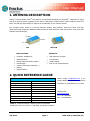
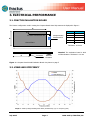
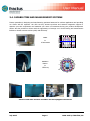
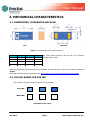
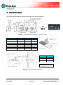
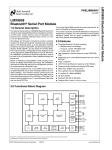
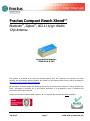
Fractus Compact Reach Xtend™ Bluetooth®, Zigbee®, 802.11 b/g/n WLAN Chip Antenna Antenna Part Number: FR05-S1-N-0-102 This product is protected by at least the following patents PAT. US 7,148,850, US 7,202,822 and other domestic and international patents pending. Any update on new patents linked to this product will appear in http://www.fractus.com/index.php/fractus/patents All information contained within this document is property of Fractus and is subject to change without prior notice. Information is provided “as is” and without warranties. It is prohibited to copy or reproduce this information without prior approval. Fractus is an ISO 9001:2008 certified company. All our antennas are lead-free and RoHS compliant. July 2015 Page 1 1999-2015 © FRACTUS, S.A. TABLE OF CONTENTS 1. ANTENNA DESCRIPTION __________________________________________________________________ 3 2. QUICK REFERENCE GUIDE _________________________________________________________________ 3 3. ELECTRICAL PERFORMANCE _______________________________________________________________ 4 3.1. FRACTUS EVALUATION BOARD __________________________________________________________ 4 3.2. VSWR AND EFFICIENCY ________________________________________________________________ 4 3.3. RADIATION PATTERNS (at 2.45 GHz), GAIN AND EFFICIENCY _________________________________ 5 3.4. CAPABILITIES AND MEASUREMENT SYSTEMS ______________________________________________ 6 4. MECHANICAL CHARACTERISTICS ___________________________________________________________ 7 4.1. DIMENSIONS, TOLERANCES AND RoHS ___________________________________________________ 7 4.2. COLOUR RANGE FOR THE INK __________________________________________________________ 7 4.3. ANTENNA FOOTPRINT (AS USED IN THE EVALUATION BOARD) _______________________________ 8 5. MATCHING NETWORK ____________________________________________________________________ 8 6. ASSEMBLY PROCESS ______________________________________________________________________ 9 7. PACKAGING ____________________________________________________________________________ 11 July 2015 Page 2 1999-2015 © FRACTUS, S.A. 1. ANTENNA DESCRIPTION Fractus Compact Reach XtendTM chip antenna is engineered specifically for Bluetooth®, WLAN 802.11 b/g/n and other wireless devices operating at the ISM 2.4 GHz band. Compact Reach Xtend combines small form factor size and high performance to improve the functionality of your wireless devices. The Compact Reach Xtend is a low-cost antenna solution that combines small form factor and high performance with integration flexibility making it ideal for small consumer electronics devices such as wireless headsets and USB dongles. 7.0 mm 2.0 mm 3.0 mm TOP BOTTOM APPLICATIONS BENEFITS Headsets, Headphones Medical devices Modules WiFi, Bluetooth, Zigbee... USB Dongles Sensors (bike speed, telemetry...) Military Digital cameras High efficiency and gain Cost-effective Small footprint Easy to use (pick and place) 2. QUICK REFERENCE GUIDE Technical Features Frequency range 2.4 GHz - 2.5 GHz Average Efficiency 72.2 % Radiation Pattern Omnidirectional Peak Gain 1.7 dBi VSWR < 2:1 Polarization Linear Weight (approx.) Temperature Impedance Dimensions (L x W x H) Please contact [email protected] if you require additional information on antenna integration or optimisation on your PCB. 0.1 g -40 to + 85 ºC 50 FRACTUS S.A. www.fractus.com Tel: +34 935442690 Fax: +34 935442691 7.0 mm x 3.0 mm x 2.0 mm Table 1 -Technical Features. Measures from the evaluation board (47.0 mm x 23.0 mm x 1.0 mm PCB). See picture in page 5. July 2015 Page 3 1999-2015 © FRACTUS, S.A. 3. ELECTRICAL PERFORMANCE 3.1. FRACTUS EVALUATION BOARD The Fractus configuration used in testing the Compact Reach Xtend chip antenna is displayed in Figure 1. A D 50 Ohms transmission line Measure mm A B 41.0 23.0 C 47.0 Compact Reach Xtend Antenna B Ground Plane 8.0 E 26.0 Tolerance: ±0.2 mm C E D SMA Connector Antenna Clearance Material: The evaluation board is built on FR4 substrate. Thickness is 1.0 mm Figure 1 – Compact Reach Xtend Evaluation Board. See picture in page 5 3.2. VSWR AND EFFICIENCY Graph 1 - VSWR (Voltage Standing Wave Ratio) and Efficiency (%) vs. Frequency (GHz) July 2015 Page 4 1999-2015 © FRACTUS, S.A. 3.3. RADIATION PATTERNS (at 2.45 GHz), GAIN AND EFFICIENCY Gain (dB): Theta=90º cut 0 5 330 30 0 -5 -10 300 60 -15 -20 -25 -30 270 90 240 120 210 150 180 Orientation: Antenna in Plane ZY Azimuth Cut θ = 90º Plane XY Gain (dB): Phi=90º cut 0 5 Gain (dB): Phi=0º cut 0 5 330 0 330 30 0 -5 -5 -10 -10 300 300 60 60 -15 -15 -20 -20 -25 -25 -30 270 -30 270 90 240 120 210 150 150 180 180 Elevation Cut = 0 Plane XZ Gain Elevation Cut = 90 Plane YZ Peak Gain 1.7 dBi Average Gain across the band 1.2 dBi Gain Range across the band (min, max) Efficiency 90 240 120 210 30 0.7 dBi <-> 1.7 dBi Peak Efficiency 75.7 % Average Efficiency across the band 72.2 % Efficiency Range across the band 68.9 % - 75.7 % Table 2 – Antenna Gain and Efficiency within the 2.4-2.5 GHz band. Measures made in the evaluation board and in the Satimo STARGATE 32 anechoic chamber. July 2015 Page 5 1999-2015 © FRACTUS, S.A. 3.4. CAPABILITIES AND MEASUREMENT SYSTEMS Fractus specialises in designing and manufacturing optimised antennas for wireless applications and providing our clients with RF expertise. We offer turn-key antenna products and antenna integration support to minimise your time requirement and maximize your return on investment during your product development efforts. We also provide our clients with the opportunity to leverage our in-house testing and measurement facilities to obtain accurate results quickly and efficiently. 0 Le ft Ante nna Rig ht Ante nna Is o latio n -2 -6 Re turn Lo s s (dB) VSWR & S Parameters -4 -8 VSWR=2 -10 -12 -14 -16 -18 Agilent E5071B -20 2 2.5 3 3.5 4 4.5 Fre que nc y (GHz) 0 5 5.5 6 5 330 0 30 -5 Radiation Pattern & Efficiency -10 300 60 -15 -20 -25 -30 270 90 240 120 f=5350MHz 210 SATIMO STARGATE 32 150 180 Anechoic and semi-anechoic chambers and full equipped in-house lab July 2015 Page 6 1999-2015 © FRACTUS, S.A. 4. MECHANICAL CHARACTERISTICS 4.1. DIMENSIONS, TOLERANCES AND RoHS TOP BOTTOM Figure 2 – Antenna Dimensions and Tolerances Measure mm Measure mm A 7.0 0.2 E 1.1 0.1 B 3.0 0.2 F 2.2 0.1 C 2.0 0.2 G 4.0 0.2 D 0.4 0.15 The white square located on the top side of the antenna indicates the feed pad. Fractus Compact Reach Xtend chip antenna is compliant with the restriction of the use of hazardous substances (RoHS). The RoHS certificate can be downloaded from http://www.fractus.com/index.php/fractus/documentation 4.2. COLOUR RANGE FOR THE INK The next figure shows the range of the colours in the antenna: Blue INK: White INK: Acceptable colour range July 2015 Page 7 1999-2015 © FRACTUS, S.A. 4.3. ANTENNA FOOTPRINT (as used in the evaluation board) This antenna footprint applies for the reference evaluation board described in page 4 of this User Manual. Feeding line dimensions over the clearance zone described in figure 3 applies for a 1 mm thickness FR4 PCB. Measure mm A 7.0 B 3.0 C D 1.5 0.2 E 2.6 F 3.6 G 3.0 H 0.5 I 4.7 J 1.5 Tolerance: ±0.2 mm Figure 3 – Antenna Footprint Details Other PCB form factors and configurations may require a different feeding configuration, feeding line dimensions and clearance areas. If you require support for the integration of the antenna in your design, please contact [email protected] 5. MATCHING NETWORK The specs of a Fractus standard antenna are measured in their evaluation board, which is an ideal case. In a real design, components nearby the antenna, LCD’s, batteries, covers, connectors, etc affect the antenna performance. This is the reason why it is highly recommended to place 0402 pads for a PI matching network as close as possible to the antenna feeding point. Do it in the ground plane area, not in the clearance area. This is a degree of freedom to tune the antenna once the design is finished and taking into account all elements of the system (batteries, displays, covers, etc). July 2015 Page 8 1999-2015 © FRACTUS, S.A. 6. ASSEMBLY PROCESS Figure 4 shows the back and front view of the Compact Reach Xtend chip antenna, which indicates the location of the feeding point and the mounting pad: Mounting Pad (2): solder the antenna mounting pad to the soldering pad on the PCB. This pad must NOT be grounded. 1 2 Feed Pad (1): the white square on the top of the antenna indicates the position of the feed pad in the bottom. Align the feed point with the feeding line on the PCB. See Figure 1. Figure 4 –Pads of the Compact Reach Xtend Chip Antenna. As a surface mount device (SMD), this antenna is compatible with industry standard soldering processes. The basic assembly procedure for this antenna is as follows: 1. Apply a solder paste on the pads of the PCB. Place the antenna on the board. 2. Perform a reflow process according to the temperature profile detailed in table 3, figure 6 of page 10. 3. After soldering the antenna to the circuit board, perform a cleaning process to remove any residual flux. Fractus recommends conducting a visual inspection after the cleaning process to verify that all reflux has been removed. The drawing below shows the soldering details obtained after a correct assembly process: Antenna Antenna Solder Paste ~ 0.1* mm PCB PCB Figure 5 - Soldering Details NOTE(*): Solder paste thickness after the assembly process will depend on the thickness of the soldering stencil mask. A stencil thickness equal or larger than 127 microns (5 mils) is required. July 2015 Page 9 1999-2015 © FRACTUS, S.A. Fractus Compact Reach Xtend chip antenna can be assembled following the Pb-free assembly process. According to the Standard IPC/JEDEC J-STD-020C, the temperature profile suggested is as follows: Phase Profile features Pb-Free Assembly (SnAgCu) RAMP-UP Avg. Ramp-up Rate (Tsmax to Tp) 3 ºC / second (max.) PREHEAT - Temperature Min (Tsmin) 150 ºC - Temperature Max (Tsmax) 200 ºC - Time (tsmin to tsmax) 60-180 seconds - Temperature (TL) 217 ºC - Total Time above TL (t L) 60-150 seconds - Temperature (Tp) 260 ºC - Time (tp) 20-40 seconds Rate 6 ºC/second max. REFLOW PEAK RAMP-DOWN Time from 25 ºC to Peak Temperature 8 minutes max. Table 3 – Recommended soldering temperatures Next graphic shows temperature profile (grey zone) for the antenna assembly process in reflow ovens. Figure 6 – Temperature profile July 2015 Page 10 1999-2015 © FRACTUS, S.A. 7. PACKAGING The Compact Reach Xtend chip antenna is delivered in tape and reel packaging. Figure 7 –Tape dimensions & real image including antennas Measure mm Measure mm TAPE WIDTH (W) 16.0 ± 0.3 Wmax 16.3 A0 3.6 ± 0.1 E 1.7 ± 0.1 B0 K0 7.5 ± 0.1 2.5 ± 0.1 F K 7.5 ± 0.1 2.8 ± 0.1 B1 8.1 ± 0.1 P 8.0 ± 0.1 D 1.55 ± 0.05 P0 4.0 ± 0.1 D1 1.55 ± 0.05 P2 2.0 ± 0.1 Measure A mm 330 ± 1 G 17.5 ± 0.2 t max 21.5 ± 0.2 Reel Capacity: 2500 pcs. Figure 8 – Reel Dimensions and Capacity July 2015 Page 11 1999-2015 © FRACTUS, S.A.