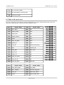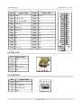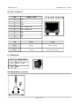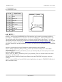
1
STM32-P207 development board
USER’S MANUAL
Revision D, May 2014
Designed by OLIMEX Ltd, 2011
All boards produced by Olimex LTD are ROHS compliant
OLIMEX© 2014
STM32-P207 user's manual
Disclaimer:
© 2014 Olimex Ltd. Olimex®, logo and combinations thereof, are registered trademarks of Olimex Ltd.
Other product names may be trademarks of others and the rights belong to their respective owners.
The information in this document is provided in connection with Olimex products. No license, express
or implied or otherwise, to any intellectual property right is granted by this document or in connection
with the sale of Olimex products.
The hardware and the software files are closed source and would not be distributed nor shared.
It is possible that the pictures in this manual differ from the latest revision of the board.
The product described in this document is subject to continuous development and improvements. All
particulars of the product and its use contained in this document are given by OLIMEX in good faith.
However all warranties implied or expressed including but not limited to implied warranties of
merchantability or fitness for purpose are excluded. This document is intended only to assist the reader in the
use of the product. OLIMEX Ltd. shall not be liable for any loss or damage arising from the use of any
information in this document or any error or omission in such information or any incorrect use of the
product.
This product is intended for use for engineering development, demonstration, or evaluation purposes only
and is not considered by OLIMEX to be a finished end-product fit for general consumer use. Persons
handling the product must have electronics training and observe good engineering practice standards. As
such, the goods being provided are not intended to be complete in terms of required design-, marketing-,
and/or manufacturing-related protective considerations, including product safety and environmental
measures typically found in end products that incorporate such semiconductor components or circuit boards.
Olimex currently deals with a variety of customers for products, and therefore our arrangement with the user
is not exclusive. Olimex assumes no liability for applications assistance, customer product design, software
performance, or infringement of patents or services described herein.
THERE IS NO WARRANTY FOR THE DESIGN MATERIALS AND THE
COMPONENTS USED TO CREATE STM32-P207. THEY ARE CONSIDERED
SUITABLE ONLY FOR STM32-P207
Page 2 of 34
OLIMEX© 2014
STM32-P207 user's manual
Table of Contents
CHAPTER 1 OVERVIEW......................................................................................... 5
1. Introduction to the chapter.......................................................................................................5
1.1 Features.....................................................................................................................................5
1.2 Organization.............................................................................................................................6
CHAPTER 2 SETTING UP THE STM32-P207 BOARD....................................... 7
2. Introduction to the chapter.......................................................................................................7
2.1 Electrostatic warning...............................................................................................................7
2.2 Requirements........................................................................................................................... 7
2.3 Powering the board..................................................................................................................8
2.4 Prebuilt software......................................................................................................................8
CHAPTER 3 STM32-P207 BOARD DESCRIPTION.............................................9
3. Introduction to the chapter.......................................................................................................9
3.1 Layout (top view).....................................................................................................................9
3.2 Layout (bottom view).............................................................................................................10
CHAPTER 4 THE STM32F207ZET6 MICROCONTROLLER..........................11
4. Introduction to the chapter..................................................................................................... 11
4.1 The microcontroller............................................................................................................... 11
5. Introduction to the chapter.....................................................................................................13
5.1 Reset........................................................................................................................................13
5.2 Clock....................................................................................................................................... 13
CHAPTER 6 HARDWARE......................................................................................14
6. Introduction to the chapter.....................................................................................................14
6.1 JTAG connector..................................................................................................................... 14
6.2 UEXT...................................................................................................................................... 15
6.3 Pads on the proto area...........................................................................................................16
6.4 USB_OTG...............................................................................................................................17
6.5 USB HOST..............................................................................................................................17
6.6 LAN connector.......................................................................................................................18
6.7 PWR Jack...............................................................................................................................18
6.8 Headphones connector.......................................................................................................... 18
6.9 SD/MMC slot..........................................................................................................................19
6.10 RS232_1................................................................................................................................ 19
6.11 RS232_2.................................................................................................................................21
6.12 CAN connector.....................................................................................................................22
6.13 Battery connector.................................................................................................................22
6.14 Jumper description..............................................................................................................22
6.15 LCD Display with backlight................................................................................................24
Page 3 of 34
OLIMEX© 2014
STM32-P207 user's manual
6.16 VGA Color Camera............................................................................................................. 24
6.17 Additional hardware components...................................................................................... 25
6.18 Notes on interfaces...............................................................................................................25
CHAPTER 7 MEMORY...........................................................................................27
7. Introduction to the chapter.....................................................................................................27
7.1 Memory map.......................................................................................................................... 28
CHAPTER 8 SCHEMATICS...................................................................................29
8. Introduction to the chapter.....................................................................................................29
8.1 Eagle schematic......................................................................................................................29
8.2 Physical dimensions...............................................................................................................31
CHAPTER 9 REVISION HISTORY.......................................................................32
9. Introduction to the chapter.....................................................................................................32
9.1 Document revision................................................................................................................. 32
9.2 Web page of your device........................................................................................................33
9.3 Product support..................................................................................................................... 34
Page 4 of 34
OLIMEX© 2014
STM32-P207 user's manual
CHAPTER 1 OVERVIEW
1. Introduction to the chapter
Thank you for choosing the STM32-P207 development board from Olimex! This document
provides a user’s guide for the Olimex STM32-P207 development board. As an overview, this
chapter gives the scope of this document and lists the board’s features. The document’s organization
is then detailed.
The STM32-P207 development board enables code development of applications running on the M3
CORTEX STM32F207ZET6 microcontroller, manufactured by STMicroelectronics.
1.1 Features
•
•
•
•
•
•
•
•
•
•
•
•
•
•
•
•
•
•
•
•
•
•
•
•
•
CPU: STM32F207ZET6 120Mhz 32 bit ARM-based microcontroller with 512 KB Flash,
128 (112+16) KB RAM, USB OTG HS and USB OTG HS, Ethernet, 14 timers, 3 SPI, 3
I2C, Ethernet, 2 CANs, 3 12 bit ADCs, 2 12 bit DACs, 114 GPIOs, Camera interface
TAG connector with ARM 2x10 pin layout for programming/debugging
512 KB fast external SRAM on board
4 Status LEDs
Stereo Audio Codec CS4344
CAN driver
Temperature sensor
Trimmer potentiometer
Joystick for navigation
6610 LCD color 128x128 pixel TFT display
SAMSUNG E700 VGA camera 640x480 color
Tamper and Wakeup buttons
2 RS232 drivers and connectors
25 Mhz quartz crystal
USB_OTG
USB_HOST
100 Mbit Ethernet
Mini SD/MMC card connector
UEXT connector
Power Jack
RESET button and circuit
Power-on led
3V battery connector
Extension port connectors for many of microcontrollers pins
PCB: FR-4, 1.5 mm (0,062"), soldermask, silkscreen component print
Page 5 of 34
OLIMEX© 2014
•
STM32-P207 user's manual
Dimensions: 160x116 mm (6.3x4.6")
1.2 Organization
Each section in this document covers a separate topic, organized as follow:
– Chapter 1 is an overview of the board usage and features
– Chapter 2 provides a guide for quickly setting up the board
– Chapter 3 contains the general board diagram and layout
– Chapter 4 describes the component that is the heart of the board: the STM32F207ZET6
microcontroller
– Chapter 5 is an explanation of the control circuitry associated with the microcontroller to
reset. Also shows the clocks on the board
– Chapter 6 covers the connector pinout, peripherals and jumper description
– Chapter 7 shows the memory map
– Chapter 8 provides the schematics
– Chapter 9 contains the revision history
Page 6 of 34
OLIMEX© 2014
STM32-P207 user's manual
CHAPTER 2 SETTING UP THE STM32-P207 BOARD
2. Introduction to the chapter
This section helps you set up the STM32-P207 development board for the first time.
Please consider first the electrostatic warning to avoid damaging the board, then discover the
hardware and software required to operate the board.
The procedure to power up the board is given, and a description of the default board behavior is
detailed.
2.1 Electrostatic warning
STM32-P207 is shipped in a protective anti-static package. The board must not be exposed to high
electrostatic potentials. A grounding strap or similar protective device should be worn when
handling the board. Avoid touching the component pins or any other metallic element.
2.2 Requirements
In order to set up the STM32-P207, the following items are required:
- 5 Vdc power supply (or JTAG or SWD, or 5V TRACE, or 5V CAN, or 5V_USB, depending on
PWR_SEL jumper position)
- SWD interface programmer
Note 1: additionally, the board can be programmed via JTAG interface but there are signals
multiplexed with the LCD and the audio, so if using JTAG interface for programming you might
need to implement a software mechanism to stop them or you might not be able to reprogram again.
Note 2: the board can also be programmed via the USART (RS232_1) connector using the built-it
bootloader application (without the need of third-party tool). This way of programming/debugging
is slow but my provide a better/cheaper solution in certain cases. The configuration is explained in
the RS232 chapter (6.10) of the manual.
You may use a pair of the following devices for this purpose:
- ARM-JTAG-COOCOX programmer/debugger which has both JTAG and SWD interfaces and
works natively with CooCox IDE, and Keil uVision and IAR EW via plugin
- Any of Olimex’s ARM-JTAG programmer/debugger (keeping in mind the note above)
- Any of Olimex's ARM-JTAG programmer/debugger + ARM-JTAG-SWD + Rowley CrossWorks
Also, a host-based software toolchain is required in order to program/debug the STM32-P207
board. There are also a number of ready IDEs available like CooCox IDE, IAR Embedded
Page 7 of 34
OLIMEX© 2014
STM32-P207 user's manual
Workbench, Rowley CrossWorks, etc.
Olimex distributes a free IDE that works with our OpenOCD programmers:
https://www.olimex.com/Products/ARM/JTAG/_resources/OpenOCD/.
At the moment of writing this guide our ARM programmers/debuggers equipped with an ARMJTAG-SWD work fine (out-of-the-box) with Rowley CrossWorks.
2.3 Powering the board
Provide +5 V DC to the board's power jack, OR +5 V via the JTAG or TRACE connector (before
providing the power set the PWR_SEL jumper in the correct position)
Additionally the board can be powered using the PROTO AREA pads. Provide 5V to the respective
pad with the same label. Ground pad is named AGND.
On powering the board the PWR LED, the SATA4 LED and the display should turn on. The
SATA1, SATA2 and SATA3 LEDs must start blinking consecutively.
If measuring the current consumption it should be around 30 mA.
2.4 Prebuilt software
On arrival the board has a basic demo installed which features test of the LEDs, the LCD, the
joystick, the camera.
IMPORTANT: If you have only a programmer with JTAG interface and you need to turn off the
peripherals using the JTAG signals press WKUP button (if there is a reset after programming you
might need to keep it pressed)! Pressing WKUP button will turn of those modules and will allow
JTAG reprogramming.
Page 8 of 34
OLIMEX© 2014
STM32-P207 user's manual
CHAPTER 3 STM32-P207 BOARD DESCRIPTION
3. Introduction to the chapter
Here you get acquainted with the main parts of the board. Note the names used on the board differ
from the names used to describe them. For the actual names check the STM32-P207 board itself.
3.1 Layout (top view)
Page 9 of 34
OLIMEX© 2014
STM32-P207 user's manual
3.2 Layout (bottom view)
Page 10 of 34
OLIMEX© 2014
STM32-P207 user's manual
CHAPTER 4 THE STM32F207ZET6 MICROCONTROLLER
4. Introduction to the chapter
In this chapter is located the information about the heart of STM32-P207 – its microcontroller. The
information is a modified version of the datasheet provided by its manufacturers.
4.1 The microcontroller
■ Core: ARM 32-bit Cortex™-M3 CPU with Adaptive real-time accelerator (ART Accelerator™)
allowing 0-wait state execution performance from Flash memory, frequency up to 120 MHz,
memory protection unit, 150 DMIPS/1.25 DMIPS/MHz (Dhrystone 2.1)
■ Memories
– 512 Kbyte of Flash memory
– 512 bytes of OTP memory
– 128 (112+16) + 4 Kbytes of SRAM
– Flexible static memory controller that supports Compact Flash, SRAM, PSRAM, NOR and
NAND memories
– LCD parallel interface, 8080/6800 modes
■ Clock, reset and supply management
– From 1.65 to 3.6 V application supply and I/Os
– POR, PDR, PVD and BOR
– 4 to 26 MHz crystal oscillator
– Internal 16 MHz factory-trimmed RC (1% accuracy at 25 °C)
– 32 kHz oscillator for RTC with calibration
– Internal 32 kHz RC with calibration
■ Low power
– Sleep, Stop and Standby modes
– VBAT supply for RTC, 20 × 32 bit backup registers, and optional 4 KB backup SRAM
■ 3 × 12-bit, 0.5 µs A/D converters
– 24 channels
– 6 MSPS in triple interleaved mode
■ 2 × 12-bit D/A converters
■ General-purpose DMA
– 16-stream DMA controller with centralized FIFOs and burst support
■ 14 timers
■ Debug mode
– Serial wire debug (SWD) & JTAG interfaces
– Cortex-M3 Embedded Trace Macrocell™
■ Up to 114 I/O ports with interrupt capability
Page 11 of 34
OLIMEX© 2014
STM32-P207 user's manual
■ Communication interfaces
– 3 × I2C interfaces (SMBus/PMBus)
– Up to 4 USARTs and 2 UARTs (7.5 Mbit/s, ISO 7816 interface, LIN, IrDA, modem control)
– 3 SPIs (30 Mbit/s), 2 with muxed I2S to achieve audio class accuracy via audio PLL or external
PLL
– 2 × CAN interfaces (2.0B Active)
– SDIO interface
■ Advanced connectivity
– USB 2.0 full-speed device/host/OTG controller with on-chip PHY
– USB 2.0 high-speed/full-speed device/host/OTG controller with dedicated DMA, on-chip fullspeed PHY and ULPI
– 10/100 Ethernet MAC with dedicated DMA: supports IEEE 1588v2 hardware, MII/RMII
■ 8- to 14-bit parallel camera interface: up to 48 Mbyte/s
■ CRC calculation unit, 96-bit unique ID
■ Analog true random number generator
For comprehensive information on the microcontroller visit the Microchip’s web page for a
datasheet.
At the moment of writing the microcontroller datasheet can be found at the following link:
http://www.st.com/internet/com/TECHNICAL_RESOURCES/TECHNICAL_LITERATURE/DAT
ASHEET/CD00237391.pdf
If the Cortex M3 processor listed above seem to lack the power or the memory for the application
you want to run, we have the same board offered with Cortex M4 one – STM32F407ZGT6. The
name of the board is STM32-P407. The table of comparison can be found below:
STM32F207ZET6
STM32F407ZGT6
Maximum speed
120Mhz
168Mhz
Program memory
512KB
1024KB
Ram memory
132KB
192KB
Page 12 of 34
OLIMEX© 2014
STM32-P207 user's manual
CHAPTER 5 CONTROL CIRCUITY
5. Introduction to the chapter
Here you can find information about reset circuit and quartz crystal locations.
5.1 Reset
STM32-P207 reset circuit includes R65(10 KΩ), R66(560 Ω), C45(100 nF), STM32F207ZET pin
25(NRST) and a RESET button. The RESET is also connected to the proto area.
5.2 Clock
25 MHz quartz crystal Q1 is connected to pins 23 and 24 of the processor.
Real time clock (RTC) Q2 is found at pins 8 and 9 of the processor.
Page 13 of 34
OLIMEX© 2014
STM32-P207 user's manual
CHAPTER 6 HARDWARE
6. Introduction to the chapter
In this chapter are presented the connectors that can be found on the board all together with their
pinout. Proto area is shown. Jumpers functions are described. Notes and info on specific peripherals
are presented. Notes regarding the interfaces are given.
6.1 JTAG connector
The 20-pin JTAG connector provides the interface for JTAG or/and SWD/TRACE
programming/debugging. It is advisable to use SWD or TRACE interface programmers.
*The JTAG TRST signal is multiplexed with the display. When using JTAG interface you will not
be able to debug the display of the board. If you wish to program the board with JTAG make sure to
hold the WKUP button when programming/debugging until you wipe the system memory or the
JTAG will not connect. This behavior is caused by the initial demo which redefines the pin to show
the display.
Another workaround is to set the bootloader jumpers so the board would attempt to boot from the
Embedded SRAM (and since it is blank, the display would not start which will allow you to debug
with the JTAG). Note this issue is not present if you use SWD interface.
JTAG/SWD interface
Pin #
Signal Name
Pin #
Signal Name
1
+3.3V
11
+3.3 V
2
+3.3V
12
GND
3
TRST/SPI1_MISO*
13
TDO/I2S3_CK
4
GND
14
GND
5
PGCTDI/I2S3_WS
15
RST
6
GND
16
GND
7
TMS
17
+5V_J-LINK
8
GND
18
GND
9
TCK
19
+5V_J-LINK
10
GND
20
GND
Page 14 of 34
OLIMEX© 2014
STM32-P207 user's manual
TRACE interface
Pin #
Signal Name
Pin #
Signal Name
1
+3.3V
11
+5V_TRACE
2
TMS
12
TEMP_ALERT
3
GND
13
+5V_TRACE
4
TCK
14
USB_HS_VBUSON
5
GND
15
GND
6
TDO/I2S3_CK
16
DCMI_D4
7
Not connected
17
GND
8
TDI/I2S3_WS
18
DCMI_D6
9
GND
19
GND
10
RST
20
DCMI_D7
6.2 UEXT
STM32-P207 board has UEXT connector and can interface Olimex's UEXT modules.
For more information on UEXT please visit:
https://www.olimex.com/Products/Modules/UEXT/
Pin #
Signal Name
1
+3.3V
2
GND
3
DCMI_D0/USART6_TX
4
USART6_RX
5
SOFTWARE SCL
6
SOFTWARE SDA
7
SD_D3/USART3_RX/SPI3_MISO
Page 15 of 34
OLIMEX© 2014
STM32-P207 user's manual
8
SD_CLK/SPI3_MOSI
9
SD_D2/USART3_TX/SPI3_SCK
10
STAT3/CS_UEXT
6.3 Pads on the proto area
For your convenience the pads are named individually near each of them. Please take extra care
about the numbering but consider that there might be offset.
PAD #
Signal Name
PAD#
Signal Name
PA0
BUT WKUP
RST
RST
PA4
DCMI_HSYNC
PG0
A10
PA5
SPI1_SCK
PG1
A11
PA6
DCMI_PIXCLK
PG2
A12
PA8
MCO1
PG3
A13
PA9
OTG_FS_VBUS
PG4
A14
PA10
DCMI_D1
PG5
A15
PB0
LCD_BL
PG6
RIGHT(JOYSTICK)
PB1
BUZ
PG9
USART6_RX
PB2
CAM_ENB
PG10
SOFT_SCL
PB5
I2S3_SD
PF15
A9
PB9
CAN1_TX
PF14
A8
PB10
USB_FS_FAULT
PF13
A7
PB12
OTG_HS_ID
PF12
A6
PB13
OTG_HS_VBUS
PF11
CAM_RST
PAD #
Signal Name
PAD#
Signal Name
PC5
ETH_RMII_RXD1
PF10
ETH_RXER
PC13
BUT TAMPER
PF9
SSTAT4/CAM_PWR
PD6
LCD_CS
PF8
STAT3/CS_UEXT
PE0
/BLE
PF7
STAT2/CAN_CTRL
Page 16 of 34
OLIMEX© 2014
PAD #
STM32-P207 user's manual
Signal Name
PAD#
Signal Name
PE1
/BHE
PF6
STAT1
PE2
TEMP_ALERT
PF5
A5
PE3
USB_HS_VBUSON
PF4
A4
PE4
DCMI_D4
PF3
A3
PE5
DCMI_D6
PF2
A2
PE6
DCMI_D7
PF1
A1
PE7
D4
PF0
A0
PE8
D5
PE15
D12
PE9
D6
PE14
D11
PE10
D7
PE13
D10
PE11
D8
PE12
D9
+5V
+5V DC
VBAT
VBAT
6.4 USB_OTG
Pin #
Signal Name
1
+5V
2
D-
3
D+
4
OTG_HS_ID
5
GND
6.5 USB HOST
PIN#
SIGNAL NAME
1
+5 V
2
USB_HOST_D-
3
USB_HOST_D+
4
GND
Page 17 of 34
OLIMEX© 2014
STM32-P207 user's manual
6.6 LAN connector
PIN#
SIGNAL
1
TX+
2
TX-
3
VDD
4
NOT CONNECTED
5
NOT CONNECTED
6
VDD
7
RX+
8
RX-
NAME
LED
Color
Usage
Right
Green
Link status
Left
Yellow
Activity status
6.7 PWR Jack
Pin #
Signal Name
1
Power Input
2
GND
6.8 Headphones connector
Page 18 of 34
OLIMEX© 2014
STM32-P207 user's manual
6.9 SD/MMC slot
Pin #
Signal Name
1
DAT2
2
DAT3/CS
3
CMD/DI
4
VDD
5
CLK/SCLK
6
VSS
7
DAT0/DO
8
DAT1
6.10 RS232_1
RS232_1 is located on USART6/SPI3 line. This interface can be used for accessing the built-in
bootloader of STM32F207 microcontroller. You will need DB9 male – DB9 female RS232 cable.
You will also need a freely distributed piece of software called “Flash Loader Demo” - it can be
downloaded from the official page of the microcontroller under the “Design resources” (by the time
of writing the resource is located here: http://www.st.com/web/en/catalog/tools/PF257525 ) . Once
you have acquired the needed perquisites we need to set the board for bootloader mode as explained
below:
Step 0. It is good idea to revert all jumpers to default positions in the beginning
Step 1. Change jumper B0_1/B0_0 to B0_1 position (as said in the table print – “Boot Mode:
System Memory”)
Step 2. RST_E and BOOT0_E should be open, as per default (if they are closed; they are located
below the RS232 connectors)
Step 3. Close TX_BOOT_E and RX_BOOT_E by soldering. They are located on the back of the
board near CAN connector.
Step 4. Download, install the Flash Loader Demo (from the STM32F207 web page, resources
window)
Step 5. Connect RS232 and run the Flash Loader Application, the target is STM32F2_512K (check
the screenshots below).
Page 19 of 34
OLIMEX© 2014
STM32-P207 user's manual
More information might be found in these documents:
1) http://www.st.com/st-webui/static/active/en/resource/technical/document/datasheet/CD00237391.pdf – page 22/177
2) http://www.st.com/st-webui/static/active/en/resource/technical/document/application_note/CD00264342.pdf
Page 20 of 34
OLIMEX© 2014
Pin #
STM32-P207 user's manual
Signal Name
1
Not Connected
2
T1OUT
3
R1IN
4
RST
5
GND
6
Not Connected
7
CTS
8
Not Connected
9
Not Connected
6.11 RS232_2
RS232_2 is located on USART3 (processor pins D13 – D14, A17 – A16)
Pin #
Signal Name
1
Not connected
2
T1OUT
3
R1IN
4
Not connected
5
GND
6
Not connected
7
CTS
8
RTS
9
Not connected
Page 21 of 34
OLIMEX© 2014
STM32-P207 user's manual
6.12 CAN connector
Pin#
Signal name
1
Not connected
2
CANL
3
VSS
4
Not connected
5
VSS
6
GND
7
CANH
8
Not connected
9
+5V_CAN
6.13 Battery connector
Pin #
Signal Name
1
VBAT
2
GND
6.14 Jumper description
Most of the jumper configurations are printed with white print on the PCB for your convenience.
PWR_SEL
On the setting of this jumper depends the way we power the board. There is a table printed on the
board with the positions. You can check the table below also. Position 1-2 is the one at the PWR
connector side.
PWR_SEL
1 - 2
+5V_EXT
3 - 4
+5V_J-LINK
5 - 6
+5V_CAN
Page 22 of 34
OLIMEX© 2014
STM32-P207 user's manual
7 - 8
+5V_USB_OTG
9 - 10
+5V_TRACE
Default position is 3-4.
STAT1_E, STAT2_E, STAT3_E, STAT4_E
Those 4 jumpers control whether the LEDs are powered(closed) or not(open).
Default state is closed.
BOOT0_E
Connected to pin 138 (BOOT0/VPP), enables boot if open.
Default state is open.
RST_E
Controls the RST on the RS232_1. If closed is present. Default state is not present.
Default state is open.
B1_1/B1_0, B0_1/B0_0
These jumpers should be moved together and control which memory would be used to load code
initially. There is a table printed on the board, describing the positions.
Default state is B1_0, B0_0.
3.3V_MCU_EN
When closed enables the power supply on the STM32F207ZET.
Default state is closed.
TX_BOOT_E
If closed separates USART6_TX and PC10.
Default state is open.
Page 23 of 34
OLIMEX© 2014
STM32-P207 user's manual
RX_BOOT_E
If closed separates USART6_RX and PC11.
Default state is open.
3.3V_E
Board's digital power supply is disabled if open.
Enabled if closed.
Default state is open.
AGND_E
Analog GND is disabled if open.
If closed Analog GND is enabled.
Default state is closed.
R-T
RST and TRST are separated if open.
RST and TRST are connected if closed.
Refer to the schematic near the JTAG connector for how this jumper influences the JTAG
programming of the board.
Default state is open.
CAN_T
Can termination is disabled if open.
Default state is open.
6.15 LCD Display with backlight
replica of Nokia 6610 color display 128x128 pixels
6.16 VGA Color Camera
640x480 pixels (0.3 mega pixel) Samsung 700 camera + connector
6.17 Additional hardware components
The components below are mounted on STM32-P207 but are not discussed above. They are listed
Page 24 of 34
OLIMEX© 2014
STM32-P207 user's manual
here for completeness:
Joystick
Temperature sensor
Audio out
Trimmer
Buzzer
Additional memory
2 buttons + RST button
4 status LEDs + PWR LED
6.18 Notes on interfaces
Note that due the evaluation nature of the board not all interfaces are immediately available on the
proto area. Some of the signals are used by peripherals and other devices.
One of those interfaces were the 3 x I2C which were sacrificed for additional peripherals and
signals that are hard to implement on software level.
There are ways, of course. Depends on which interface you are willing to let go. I will list the
options in the following order (I2C number - processor pin - signal - interface affected):
I2C1_SCL - 139 - CAN1_RX - CAN interface
I2C1_SDA - 140 - CAN1_TX - CAN interface
I2C2_SCL - 11 - A0 - the additional memory
I2C2_SDA - 10 - A1 - the additional memory
I2C3_SCL - 100 - MCO1 - camera interface
I2C3_SDA - 99 - SD_D1/DCMI_DB - SD card / camera
To my mind, the best idea would be to disable the CAN interface.
When you have chosen the preferred I2C port you need to decide whether to remove the peripheral
it is connected to or to disable it by software means (instead of removing components just always
set the needed signals as outputs - disable input and connect additional wires). The final thing to do
Page 25 of 34
OLIMEX© 2014
STM32-P207 user's manual
is to use 2.2k pull-up resistors on the lines you have chosen (for instance I2C1_SCL and
I2C1_SDA) - I2C requires pull-ups.
Page 26 of 34
OLIMEX© 2014
STM32-P207 user's manual
CHAPTER 7 MEMORY
7. Introduction to the chapter
On the next page you can find a memory map for this family of processors. It is strongly
recommended to refer to the original datasheet released by STMicroelectronics for one of higher
quality.
Page 27 of 34
OLIMEX© 2014
STM32-P207 user's manual
7.1 Memory map
Page 28 of 34
OLIMEX© 2014
STM32-P207 user's manual
CHAPTER 8 SCHEMATICS
8. Introduction to the chapter
In this chapter are located the schematics describing logically and physically STM32-P207.
8.1 Eagle schematic
STM32-P207 schematic is visible for reference here. You can also find them on the web page for
STM32-P207 at our site: https://www.olimex.com/Products/ARM/ST/STM32P207/resources/STM32-P207-P407_rev_D.pdf. They are located in HARDWARE section.
The EAGLE schematic is situated on the next page for quicker reference.
Page 29 of 34
OLIMEX© 2014
STM32-P207 user's manual
D15
LEFT
A<1>
D<6>
RIGHT
C<3>
DOWN
RM5G4
LEFT
CENTER
1k
RM5G2
CENT
DOWN
1k
RM5G1
DOWN
1k
R81
RIGHT
33k
33k
RM6G4
1k
RM5G3
10
+
PF0
PF1
PF2
PF3
PF4
PF5
PF6
PF7
PF8
PF9
PF10
PF11
PF12
PF13
PF14
PF15
A0
A1
A2
A3
A4
A5
STAT1
10
11
12
13
14
15
18
ST A T 2/CAN_CT RL 19
ST A T 3/CS_UEXT
20
ST A T 4/CAM _P WR 21
22
ETH_RXER
49
CAM_RST
A6
50
A7
53
A8
54
A9
55
NRST
PG0/FSMC_A10
PG1/FSMC_A11
PG2/FSMC_A12
PG3/FSMC_A13
PG4/FSMC_A14
PG5/FSMC_A15
PG6/FSMC_INT2
PG7/FSMC_INT3/USART6_CK
PG8/USART6_RTS/ETH_PPS_OUT
PG9/USART6_RX/FSMC_NE2/FSMC_NCE3
PG10/FSMC_NCE4_1/FSMC_NE3
PG11/FSMC_NCE4_2/ETH_MII_TX_EN
PG12/FSMC_NE4/USART6_RTS
PG13/FSMC_A24/USART6_CTS/ETH_MII_TXD0/ETH_RMII_TXD0
PG14/FSMC_A25/USART6_TX/ETH_MII_TXD1/ETH_RMII_TXD1
PG15/USART6_CTS/DCMI_D13
PF0/FSMC_A0/I2C2_SDA
PF1/FSMC_A1/I2C2_SCL
PF2/FSMC_A2/I2C2_SMBA
PF3/FSMC_A3/ADC3_IN9
PF4/FSMC_A4/ADC3_IN14
PF5/FSMC_A5/ADC3_IN15
PF6/TIM10_CH1/FSMC_NIORD/ADC3_IN4
PF7/TIM11_CH1/FSMC_NREG/ADC3_IN5
PF8/TIM13_CH1/FSMC_NIOWR/ADC3_IN6
PF9/TIM14_CH1/FSMC_CD/ADC3_IN7
PF10/FSMC_INTR/ADC3_IN8
PF11/DCMI_12
PF12/FSMC_A6
PF13/FSMC_A7
PF14/FSMC_A8
PF15/FSMC_A9
PE0/TIM4_ETR/FSMC_NBL0/DCMI_D2
PE1/FSMC_NBL1/DCMI_D3
PE2/TRACECK/FSMC_A23/ETH_MII_TXD3
PE3/TRACED0/FSMC_A19
PE4/TRACED1/FSMC_A20/DCMI_D4
PE5/TRACED2/FSMC_A21/TIM9_CH1/DCMI_D6
PE6/TRACED3/FSMC_A22/TIM9_CH2/DCMI_D7
PE7/FSMC_D4/TIM1_ETR
PE8/FSMC_D5/TIM1_CH1N
PE9/FSMC_D6/TIM1_CH1
PE10/FSMC_D7/TIM1_CH2N
PE11/FSMC_D8/TIM1_CH2
PE12/FSMC_D9/TIM1_CH3N
PE13/FSMC_D10/TIM1_CH3
PE14/FSMC_D11/TIM1_CH4
PE15/FSMC_D12/TIM1_BKIN
UP
1k
TAMPER
WKUP
TAMPER
330R
C46
R111
OTG_HS_DP
R109
15R
OTG_HS_DM
R110
15R
0R
4
C55
100uF/10V/TANT D
+
IS
DC
VCC
VSS
+
100nF
7
8
6
1
2
3
4
0R(NA)
RM4G2
RM4G1
33k
33k
U3
4
L5
8
#ENA
OUT_A 7
FLAG_A
IN 6
FLAG_B
GND 5
#ENB
OUT_B
LM3526-L(SO-8)
USB_OTG
3.3V
C58
USB_OTG
4
47pF(NA)
100nF
U6
VSS
GND1
GND2
+5V_OTG_PWR
USB_OTG_DUSB_OTG_D+
OTG_HS_ID
C62
D4
2.2uF/6.3V
NA(ESDA6V1L)
OTG_HS_VBUS
OTG_HS_ID
3
+5V_OTG_PWR
USB_OTG_DUSB_OTG_D+
OTG_HS_ID
VBUS
DD+
ID
GND
USB
C57
3
2
1
L6
USB-OTG
2
6NC2-50MHz
CAN DRIVER
LCD_BL
BUZ
CAM_ENB
TDO/I2S3_CK
TRST/SPI1_MISO
I2S3_SD
DCMI_D5
DCMI_VSYNC
CAN1_RX
CAN1_TX
USB_FS_FAULT
ETH_RMII_TX_EN
OTG_HS_ID
OTG_HS_VBUS
OTG_HS_DM
OTG_HS_DP
PB0
PB1
PB2
26
27
28
29
44
45
96
97
98
99
111
112
113
7
8
9
TRIM
ETH_RMII_MDC
USB_FS_VBUSON
SOFT_SPI1_MOSI
ETH_RMII_RXD0
ETH_RMII_RXD1
PC5
DCMI_D0/USART6_TX
I2S3_MCK
SD_D0/DCMI_D2
SD_D1/DCMI_D3
SD_D2/USART3_TX/SPI3_SCK
SD_D3/USART3_RX/SPI3_MISO
SD_CLK/SPI3_MOSI
TAMPER
PC13
114
115
116
117
118
119
122
123
77
78
79
80
81
82
85
86
D2
D3
SD_CMD
LCD_RST
/OE
R92
10k
/WE
LCD_CS
NE1
D13/USART3_TX
D14/USART3_RX
D15
A16/USART3_CTS
A17/USART3_RTS
USB_HS_FAULT
D0
D1
141
142
1
2
3
4
5
58
59
60
63
64
65
66
67
68
/BLE
/BHE
TEMP_ALERT
USB_HS_VBUSON
DCMI_D4
DCMI_D6
DCMI_D7
D4
D5
D6
D7
D8
D9
D10
D11
D12
R93
NA
R154
NA
R116
10k
CAN1_TX
1
2
3
4
CAN1_RX
PA8
PA9
PA10
C64
TXD
VSS
VDD
RXD
8
RS 7
CANH 6
CANL 5
VREF
R118
NA
R119
NA
DB9-Male
R120
NA
R121
10k
C
D
E
F
1
2
3
R122
560R
SDA VDD 8
SCL
7
ALERT A0
6
A1 5
GND
A2
C65
(#OS /INT )
R123
R124
TCN75AVUA(TSSOP8)
4
100nF
NA
0R(NA)
0R
LCD_BL
4.7k
R94
PB5
B1_1/B1_0
HN1x3(B1_1:Open;B1_0:Cl ose)
C75
10uF/6.3V/0805
C74 470pF
PB12
PB13
Q2
32768Hz/6pF
R128
3.3V_A
C66
1
2
3
4
9
8
C67
100nF
10uF/6.3V/0805
330R
C69
SDIN
VQ
#DEM/SCLK
LRCK
FILT+
MCLK
AOUTL
VA
GNDA AOUTR
5
R125
NA
+
6
10uF/6.3V/0805
C70
7
10uF/6.3V/0805
R126
C11 2.2uF/6.3V
C68 100nF
U9
I2S3_SD
TDO/I2S3_CK
TDI/I2S3_WS
I2S3_MCK
C72
2.2nF
C76
20k
R127
100nF
4
20k
3
C73
U10
5
8
+
C77
10uF/6.3V/0805
TS4871ID(SO-8)
2.2uF/6.3V
HEADPHONES
+
1-L
3.3V_A
10
C81 470pF
R132
C49 15pF
C12 2.2uF/6.3V
3.3V
PD6
R130
R131
330R
20k
C79
2.2nF
R129
NA
4
3
3-R
SCJ325P00XG0B02G
C82
100nF
20k
C80
4
2
C84
10uF/6.3V/0805
CS4344-CZZ(10-TSSOP)
C50 15pF
GN D
5
3.3V_A
AUDIO OUT
3.3V
U11
5
8
+
C83
10uF/6.3V/0805
TS4871ID(SO-8)
2.2uF/6.3V
3
PE0
PE1
PE2
PE3
PE4
PE5
PE6
PE7
PE8
PE9
PE10
PE11
PE12
PE13
PE14
PE15
RS232 DRIVERS
SD/MMC CARD
RST_E
RST
U12PWR
16VCC
3.3V
C86
1
100nF
5
D13/USART3_TX
A17/USART3_RTS
C48
D14/USART3_RX
A16/USART3_CTS
11
10
R133
330R
12
9
R134
330R
WKUP
C1+
C1C2+
V+
V-
16VCC
3.3V
R1OUT
R2OUT
2
6
C88
100nF
C89
100nF
R1IN
R2IN
1
2
3
4
5
13
8
TX_BOOT_E
Open
6
7
8
9
3
5
DCMI_D0/USART6_TX
11
R136
10
0R
0R(NA)
USART6_RX
12
R137
9
330R
BOOT0_E
DB9-Female
USART6_RX
C91
1
100nF
C92
4
100nF
NA
RS232_2
14
7
ST3232CDR(SO16)
330R
RX_BOOT_E
Open
R135
T1OUT
T2OUT
GND15
R51
33k
10 k
C90
100nF
C2T1IN
T2IN
T2
DTC114YKA
U13PWR
SD_D2/USART3_TX/SPI3_SCK
SD_D3/USART3_RX/SPI3_MISO
GND15
C85
100nF
U12
3.3V 3.3V 3.3V
Set-up in SPI-Mode
HN1x2(Open)
U13
C1+
C1C2+
V+
V-
2
6
C93
100nF
C94
100nF
SD_D3/US ART 3_RX/SP I3_MISO
SD_CMD
SD_CLK/S PI3_M OSI
SD_D0/DCMI_D2
SD_D1/DCMI_D3
SD_D2/US ART 3_T X/SP I3_SCK
C2T1IN
T2IN
R1OUT
R2OUT
T1OUT
T2OUT
R1IN
R2IN
14
7
13
8
ST3232CDR(SO16)
D6
1N4148
BOOT0
RS232_1
1
2
3
4
5
6
7
8
9
3.3V
3.3V
3.3V
DB9-Female
R139
NA
R29
R24
R22
R30
R31
R25
R26
R27
R28
R32
0R
NA
NA
0R
0R
NA
NA
NA
NA
0R
R34
R35
R37
33k
33k
33k
R53
NA
R8
1M
C95
2
SD/MMC
2
3
6
4
5
7
8
1
CD/DAT3/CS
CMD/DI
VSS
VDD
CLK/SCLK
DAT0/DO
DAT1/RES
DAT2/RES
MICRO
47uF/6.3V/TANT
1
HN1x2(Open)
G
H
I
Page 30 of 34
6
U8
SOFT_SDA
SOFT_SCL
TEMP_ALERT
+5V_CAN
R117
120R
CAN_T
Open
3.3V
3.3V
3.3V
6
7
8
9
SN65HVD230(SO8)
100nF
PB9
PB10
TEMPERATURE SENSOR
CAN
1
2
3
4
5
U7
+
46
47
48
133
134
135
136
137
139
140
69
70
73
74
75
76
STAT2/CAN_CTRL
3.3V
PA4
PA5
PA6
6
1
PA0
VC C
WKUP
ETH_RMII_REF_CLK
ETH_RMII_MDIO
ETH_RMII_MDINT
DCMI_HSYNC
SPI1_SCK
DCMI_PIXCLK
ETH_RMII_CRS_DV
MCO1
OTG_FS_VBUS
DCMI_D1
OTG_FS_DM
OTG_FS_DP
TMS
TCK
TDI/I2S3_WS
GN D
34
35
36
37
40
41
42
43
100
101
102
103
104
105
109
110
6.11.2012 3. 09:11:54 G.
B
7
FB0805/600R/200mA(201209-601)
STM32-P207
A
8
SHIELD
USB_A
GND3
GND4
47pF(NA)
4
5
6
USB
100nF C61
C60
+
10uF/6.3V/TANT
3.3V
C59
33k
33k
100nF C63
33k
VDD
R87
33k
100nF
RM4G4
RM4G3
USB_HOST
+5V_HOST_PWR 1
USB_HOST_D2
USB_HOST_D+
3
FB0805/600R/200mA(201209-601)
100nF
1k
1k
E/D
C87
4
100nF
100nF
R88
OTG_HS_VBUS
CD1
3.3V
BUTTONS
R84
NA(ESDA6V1L)
USB_FS_VBUSON
USB_FS_FAULT
USB_HS_FAULT
USB_HS_VBUSON
C56
R85
+5V
NA(USBLC6-2P6)
3.3V
1
D5
NA(USBLC6-2P6)
3.3V
3
R83
33k
100nF
ETH_RXER
NA
STM32F207ZET6
3.3V
C98
47pF(NA)
USB_FS_VBUSON
USB_FS_FAULT
ETH_RMII_CRS_DV
OUT
PD0/FSMC_D2/CAN1_RX
PD1/FSMC_D3/CAN1_TX
PD2/TIM3_ETR/UART5_RX/SDIO_CMD/DCMI_D11
PD3/FSMC_CLK/USART2_CTS
PD4/FSMC_NOE/USART2_RTS
PD5/FSMC_NWE/USART2_TX
PD6/FSMC_NWAIT/USART2_RX
PD7/USART2_CK/FSMC_NE1/FSMC_NCE2
PD8/FSMC_D13/USART3_TX
PD9/FSMC_D14/USART3_RX
PD10/FSMC_D15/USART3_CK
PD11/FSMC_A16/USART3_CTS
PD12/FSMC_A17/TIM4_CH1/USART3_RTS
PD13/FSMC_A18/TIM4_CH2
PD14/FSMC_D0/TIM4_CH3
PD15/FSMC_D1/TIM4_CH4
C99
+
PH1/OSC_OUT
9
R108
1.2k/1%
USB_HOST
+5V_HOST_PWR
USB_HOST_DUSB_HOST_D+
1
2
3
7
2
24
23
22
21
20
19
18
17
16
15
14
13
C100
47pF(NA)
6
5
4
6
1
56
57
87
88
89
90
91
92
93
124
125
126
127
128
129
132
PH0/OSC_IN
MC34063(SO8)
470pF
VC C
A10
A11
A12
A13
A14
A15
RIGHT
UP
DOWN
PG9
USART6_RX
PG10
SOFT_SCL
LEFT
SOFT_SDA
ETH_RMII_TXD0
ETH_RMII_TXD1
CENT
25
BOOT0/VPP
R107
5.6k/1%
5
FB
USB CIRCUIT
U5
ETH_RMII_MDIO
ETH_RMII_MDC
R13
C16
0R(NA)
1
100nF C37
100nF C36
100nF C35
100nF C34
100nF C33
STAT1
STAT1
STAT2/CAN_CTRL
STAT3/CS_UEXT
STAT4/CAM_PWR
PG0
PG1
PG2
PG3
PG4
PG5
PG6
24
15R
0R
2
100nF
15R
R152
ETH_RMII_RXD1
ETH_RMII_RXD0
ETH_RMII_REF_CLK
PC0/OTG_HS_ULPI_STP/ADC123_IN10
PC1/ETH_MDC/ADC123_IN11
PC2/SPI2_MISO/OTG_HS_ULPI_DIR/ETH_MII_TXD2/ADC123_IN12
PC3/SPI2_MOSI/I2S2_SD/OTG_HS_ULPI_NXT/ETH_MII_TX_CLK/ADC123_IN13
PC4/ETH_RMII_RX_D0/ETH_MII_RX_D0/ADC12_IN14
PC5/ETH_RMII_RX_D1/ETH_MII_RX_D1/ADC12_IN15
PC6/SPI2_MCK/TIM8_CH1/SDIO_D6/USART6_TX/DCMI_D0/TIM3_CH1
PC7/SPI3_MCK/TIM8_CH2/SDIO_D7/USART6_RX/DCMI_D1/TIM3_CH2
PC8/TIM8_CH3/SDIO_D0/TIM3_CH3/USART6_CK/DCMI_D2
PC9/I2S2_CKIN/I2S3_CKIN/MCO2/TIM8_CH4/SDIO_D1/I2C3_SDA/DCMI_D3/TIM3_CH4
PC10/SPI3_SCK/I2S3_CK/UART4_TX/SDIO_D2/DCMI_D8/USART3_TX
PC11/UART4_RX/SPI3_MISO/SDIO_D3/DCMI_D4/USART3_RX
PC12/UART5_TX/SDIO_CK/DCMI_D9/SPI3_MOSI/I2S3_SD/USART3_CK
PC13/RTC_AF1
PC14/OSC32_IN
PC15/OSC32_OUT
VBAT
TC
C54
1N5819S
1
2
L7
2
1
LEFT
JOYSTICK_MT5_F
R74
33k
LEFT
560R
RM6G3
33k
RIGHT
C15
RM6G1
R52
STAT4_E
G PH 254 SMT 01x02(Close)
STAT4/CAM_PWR
JOYSTICK
UP
B<4>
Common<5>
LEFT
STAT1
STAT3_E
G PH 254 SMT 01x02(Close)
STAT3/CS_UEXT
E<2>
Center push
C14
3.3V
NE1
COMMON
3.3V
11
33
12
34
K6R4016V1D-TC10
1
J1
UP
D13/USART 3_T X
D14/USART 3_RX
28
NC
VDD1
VDD2
VSS1
VSS2
GREEN(GYX-SD-TC0805SGC)
3.3V
UP
DOWN
STAT2_E
G PH 254 SMT 01x02(Close)
STAT2/CAN_CTRL
33k
CS
OE
WE
BHE
BLE
560R
RM3G4
STAT4
STAT1_E
G PH 254 SMT 01x02(Close)
RM6G2
6
41
17
40
39
RED(GYX-SD-TC0805SYRK)
100nF
NE1
/OE
/WE
/BHE
/BLE
560R
RM3G3
STAT3
D0
D1
D2
D3
D4
D5
D6
D7
D8
D9
D10
D11
D12
33k
A 16/US ART 3_CT S
A 17/US ART 3_RT S
7
8
9
10
13
14
15
16
29
30
31
32
35
36
37
38
I/O0
I/O1
I/O2
I/O3
I/O4
I/O5
I/O6
I/O7
I/O8
I/O9
I/O10
I/O11
I/O12
I/O13
I/O14
I/O15
100nF
2
YELLOW(GYX-SD-TC0805SYC)
A0
A1
A2
A3
A4
A5
A6
A7
A8
A9
A10
A11
A12
A13
A14
A15
A16
A17
3.3V
C20
PB0/TIM3_CH3/TIM8_CH2N/OTG_HS_ULPI_D1/ETH_MII_RXD2/TIM1_CH2N/ADC12_IN8
PB1/TIM3_CH4/TIM8_CH3N/OTG_HS_ULPI_D2/ETH_MII_RXD3/OTG_HS_INTN/TIM1_CH3N/ADC12_IN9
PB2/BOOT1
PB3/JTDO/TRACESWO/SPI3_SCK/I2S3_CK/TIM2_CH2/SPI1_SCK
PB4/NJTRST/SPI3_MISO/TIM3_CH1/SPI1_MISO
PB5/I2C1_SMBA/CAN2_RX/OTG_HS_ULPI_D7/ETH_PPS_OUT/TIM3_CH2/SPI1_MOSI/SPI3_MOSI/DCMI_D10/I2S3_SD
PB6/I2C1_SCL/TIM4_CH1/CAN2_TX/OTG_FS_INTN/DCMI_D5/USART1_TX
PB7/I2C1_SDA/FSMC_NL/DCMI_VSYNC/USART1_RX/TIM4_CH2
PB8/TIM4_CH3/SDIO_D4/TIM10_CH1/DCMI_D6/OTG_FS_SCL/ETH_MII_TXD3/I2C1_SCL/CAN1_RX
PB9/SPI2_NSS/I2S2_WS/TIM4_CH4/TIM11_CH1/OTG_FS_SDA/SDIO_D5/DCMI_D7/I2C1_SDA/CAN1_TX
PB10/SPI2_SCK/I2S2_CK/I2C2_SCL/USART3_TX/OTG_HS_ULPI_D3/ETH_MII_RX_ER/OTG_HS_SCL/TIM2_CH3
PB11/I2C2_SDA/USART3_RX/OTG_HS_ULPI_D4/ETH_RMII_TX_EN/ETH_MII_TX_EN/OTG_HS_SDA/TIM2_CH4
PB12/SPI2_NSS/I2S2_WS/I2C2_SMBA/USART3_CK/TIM1_BKIN/CAN2_RX/OTG_HS_ULPI_D5/ETH_RMII_TXD0/ETH_MII_TXD0/OTG_HS_ID
PB13/SPI2_SCK/I2S2_CK/USART3_CTS/TIM1_CH1N/CAN2_TX/OTG_HS_ULPI_D6/ETH_RMII_TXD1/ETH_MII_TXD1/OTG_HS_VBUS
PB14/SPI2_MISO/TIM1_CH2N/TIM12_CH1/OTG_HS_DM/USART3_RTS/TIM8_CH2N
PB15/SPI2_MOSI/I2S2_SD/TIM1_CH3N/TIM8_CH3N/TIM12_CH2/OTG_HS_DP
VSSA
SC
SE
CL470nH/0805/1.76R/250mA
STAT2
U15
1
2
3
4
5
18
19
20
21
22
23
24
25
26
27
42
43
44
2
1
560R
RM3G2
2
1
GREEN(GYX-SD-TC0805SGC)
2
1
RM3G1
STAT1
RIGHT
UP
DOWN
ETH_RMII_TXD0
ETH_RMII_TXD1
CENT
CENT
STATUS LED INDICATION
Additional MEMORY
R62
NA
VREF+
3
D3
+
3
RESET
3
R63
150R
RST
RST
100nF
138
23
560R
C45
6
U4
GN D
2
10uF
27pF
VDDA
C53
7
2
R66
RESET 1
GND
C19
27pF
C44
RST
R65
10k
U2
NA
2 VCC
1
2
GND
MCP1700T-3002E/TT
A0
A1
A2
A3
A4
A5
A6
A7
A8
A9
A10
A11
A12
A13
A14
A15
31
BOOT0
Q1
T1107A(6x3,8x2,5mm)
2.2uF
100nF
Q25.000M Hz/HC-49SM (SM D)/20pF
3.3V
3V_E
Closed
VIN
C43
VSS_11
VSS_10
VSS_9
VSS_8
VSS_7
VSS_6
VSS_5
VSS_4
VSS_2
LEDGND
GND
NOKIA6610_COLOUR_LCD
D7
10k
VOUT
32
C42
VBAT
RESET CIRCUIT
VCAP_2
22R
VREF+
R61
VR1
100nF
1k
KS8721BLMM
PA0/WKUP/USART2_CTS/USART4_TX/ETH_MII_CRS/TIM2_CH1_ETR/TIM5_CH1/TIM8_ETR/ADC123_CH0
PA1/USART2_RTS/USART4_RX/ETH_RMII_REF_CLK/ETH_MII_RX_CLK/TIM5_CH2/TIM2_CH2/ADC123_IN1
PA2/USART2_TX/TIM5_CH3/TIM9_CH1/TIM2_CH3/ETH_MDIO/ADC123_IN2
PA3/USART2_RX/TIM5_CH4/TIM9_CH2/TIM2_CH4/OTG_HS_ULPI_D0/ETH_MII_COL/ADC123_IN3
PA4/SPI1_NSS/SPI3_NSS/USART2_CK/DCMI_HSYNC/OTG_HS_SOF/I2S3_WS/ADC12_IN4/DAC1_OUT
PA5/SPI1_SCK/OTG_HS_ULPI_CK/TIM2_CH1_ETR/TIM8_CHIN/ADC12_IN5/DAC2_OUT
PA6/SPI1_MISO/TIM8_BKIN/TIM13_CH1/DCMI_PIXCLK/TIM3_CH1/TIM1_BKIN/ADC12_IN6
PA7/SPI1_MOSI/TIM8_CH1N/TIM14_CH1/TIM3_CH2/ETH_MII_RX_DV/TIM1_CH1N/RMII_CRS_DV/ADC12_IN7
PA8/MCO1/USART1_CK/TIM1_CH1/I2C3_SCL/OTG_FS_SOF
PA9/USART1_TX/TIM1_CH2/I2C3_SMBA/DCMI_D0/OTG_FS_VBUS
PA10/USART1_RX/TIM1_CH3/OTG_FS_ID/DCMI_D1
PA11/USART1_CTS/CAN1_RX/TIM1_CH4/OTG_FS_DM
PA12/USART1_RTS/CAN1_TX/TIM1_ETR/OTG_FS_DP
PA13/JTMS-SWDIO
PA14/JTCK-SWCLK
PA15/JTDI/SPI3_NSS/I2S3_WS/TIM2_CH1_ETR/SPI1_NSS
VCAP_1
VLED
R23
100nF
VBAT
3V_REG
1
100nF C32
C41
1uF
AGND
4
3
100nF C31
R60
C40
C52
1
2
3.3V
R33
10k
C13
100nF C30
D
STAT4/CAM_PWR
G
3.3V
106
33
3.3VA
1
2
3
S
3.3V_A
B0_1/B0_0
HN1x3(B0_1:Open;B0_0:Close)
FET4
BSS138
D
71
130
120
94
83
61
51
16
38
107
G
S
SOFT_SCL
RESET
9
8
0R
Q5 0R(NA)
BC817
330R
C51
10uF/6.3V/0805
R106
150R
2.2R
SCK
DIO
CS
4 7k
WF2S
SOFT_SDA
FET2
BSS138
2
R104
R103
1
2
1
2
FET1
BSS138
R64
NA
C38
2.2uF/6.3V
C39
2.2uF/6.3V
VDD_1
VDD_2
VDD_3
VDD_4
VDD_5
VDD_6
VDD_7
VDD_8
VDD_9
VDD_10
VDD_11
VDD_12
VDD_SA
T1 1 0 3 NE - DT SM - 2 1 R( 1 2 x1 2 x4 ,3 m m )
D
R14
4.7k
S
R15
4.7k
G
3V_BAT
100nF C27
D2
BAT54C
L3
+3V
+3V
R36
0R(NA)
0R
2
1
CAMERA CMOS SAMSUNG 700 + CONNECTOR
100nF C26
R16
R18
33k
NA
3.3V_MCU_EN
HN1x2(Close)
4
3
5
LCD_RST
3.3V
U1
72
108
143
39
17
52
62
84
95
121
131
30
144
3.3V
FB0805/600R/200mA(201209-601)
100nF C25
R17
R19
10k
NA
+3V
DCMI_D0/USART6_TX
DCMI_D1
SD_D0/DCMI_D2
SD_D1/DCMI_D3
DCMI_D4
DCMI_D5
DCMI_D6
DCMI_D7
C21
R151
OTG_FS_DP
+
BH10S
GND
VCC
Y0
Y1
Y2
Y3
Y4
Y5
Y6
Y7
MCK
PCK
LVL
FVL
SDA
SCL
VCC
GND
RST
ENB
CAM_RST
CAM_ENB
3.3V
R153
OTG_FS_DM
2
C18 100nF
U16
R20
33R
LAN
R12
33k
USART6_RX
SOFT_SDA
SD_CLK/SPI3_MOSI
STAT3/CS_UEXT
OTG_FS_VBUS
RST
3.3V
2
FB0805/600R/200mA(201209-601)
C17 100nF
SPI1_SCK
TRST/SPI1_MISO
LCD_CS
L4
CL220uH/SD75
R105
VDISPLAY
VDIGITAL
BL_PWR
1k
1
2
3
FB0805/600R/200mA(201209-601)
MCO1
DCMI_PIXCLK
DCMI_HSYNC
DCMI_VSYNC
CAM_SDA
CAM_SCL
2
4
6
8
10
0R(NA)
R140
1
L2
R11
2k
UEXT
1
3
5
7
9
DCMI_D0/USART6_TX
SOFT_SCL
SD_D3/USART3_RX/SPI3_MISO
SD_D2/USART3_TX/SPI3_SCK
D
0R
1
S
3.3V
1
2
3
4
5
6
7
8
9
10
11
12
MDIO
MDC
RXD3/PHYAD1
RXD2/PHYAD2
RXD1/PHYAD3
RXD0/PHYAD4
VDDIO1
GND1
RXDV/CRSDV/PCS_LPBK
RXC
RXER/ISO
GND2
1k
1k
1k
1k
R10
2k
+3V
G
100nF C29
FET3
5
3.3V
ETH_RMII_MDINT
R21
L1
6
2k
3.3V
C10 100nF
IRLML6402
2k
R98
10uF/6.3V /0805
R54
10k
R86
R146
R147
R150
R67
GND5
GND4
FXSD/FXEN
RX+
RXVDDRX
PD#
LED3/NWAYEN
LED2/DUPLEX
LED1/SPD100/NFEF
LED0/TEST
INT/PHYAD0
U14
100nF C28
10k
R96
3.3V
C78
100nF
C101
+
R55
100nF
R141
36
35
34
33
32
31
1k
30
29
NA
28
330R 27
330R 26
330R 25
3V_REG
7
BL_PWR
3.3V
6
1
3.3V
FB0805/600R/200mA(201209-601)
R2
UEXT
3.3V
3.3V
R100
33k
LCD_RST
R1
C24
100nF
3.3V
R59
3.3V
TRST/SPI1_MISO
SPI1_SCK
SOFT_SPI1_MOSI
LCD_CS
TDO/I2S3_CK
RST
TRST/SPI1_MISO
1
R99
33k
+
R142
1.5K/1%
RJLBC-060TC1
R7
33k
FB2
R4
1nF/2kV
100nF
PHY_VDD_PLL
PHY_RSTN
4.99k/1%
R3
1:1
75
C71
10uF/6.3V/0805
R145
C9
75
C47
3.3V
RM1
Y ELLOW
1
3
2
AG
KG
AY
KY
7
6
8
FB0805/600R/200mA(201209-601)
GRE EN
TD+
COM
TDAG
KG
AY
KY
RD+
NC
RD-
10k
3.3V
1:1
75
R58
+
3
7
8
6
T1
BC817
640x480 [VGA] CAMERA
NA
2
10uF/6.3V/0805
1N4148
R48
3.3V
Q
LCD
TRST/SPI1_MISO
TDI/I2S3_WS
TMS
TCK
R-T
FB3
R6
2k
10uF/6.3V/0805
10k
10k
1k
TRIMMER
C8
BUZ
PB1221P
75
P
LCD BACKLIGHT CIRCUIT
R46
NA
R102
2k
T 1 1 0 3 N E- D TS M - 2 1 R ( 1 2 x1 2 x4 ,3 m m )
330R
D1
10k
R49
R50
R45
NA
BH20S
RM2G1
1
4
5
2
3.3V
RJ45 SIDE
AN_TR
10k
+
8
TRIM
R47
R44
NA
LCD_BL
BUZ
R5
+5V_J-LINK
R43
NA
2.5V
1
LAN
BUZZER
0R
O
10
Close
3.3V_A
0R
N
R101
NA
AGND_E
2
M
1N4148
R4
560R
GND_
GND
R38
R40
R39
R41
NA
1
3
5
7
9
11
13
15
17
19
37
38
39
40
41
42
43
44
45
46
47
48
100nF
10nF
2
4
6
8
10
12
14
16
18
20
REXT
VDDRCV
GND6
TXTX+
VDDTX
GND7
GND8
XO
XI
VDDPLL
RST#
1uF
C97
TMS
TCK
TDO/I2S3_CK
TDI/I2S3_WS
RST
TEMP_ALERT
0R(NA) USB_HS_VBUSON
NA
TDO/I2S3_CK
0R(NA)
DCMI_D4
NA
TRST/SPI1_MISO
DCMI_D6
DCMI_D7
VDDIO2
GND3
CRS/RMII_BTB
COL/RMII
TXD3
TXD2
TXD1
TXD0
TXEN
TXC/REFCLK
TXER
VDDC
C7
C96
10nF
49.9R/1%
NA
49.9R/1%
49.9R/1%
49.9R/1%
R3
330R/1%
C6
+5V_TRACE
L
3.3V
R42
NA
JTAG
2
4
6
8
10
12
14
16
18
20
R9
R149
R148
R144
R143
R1
330R/1%
100uF/10V/TANT D
R2
100R/1%
PWR_LED
1
C2
+ C3
+ C1
100nF
100uF/10V/TANT D
TVS1
1.5KE6.8ALFCT
9
10uF/6.3V/0805
HN2x5(1-2:Close)
PWR
YDJ-1136
2
+ C5
VO
GND/ADJ
+ C4
VI
10uF/6.3V/0805
3
1
VR1(3.3V)
AME1085(TO263)
FUSE1
FSMD110
RED(GYX-SD-TC0805SYRK)
2
3.3V_E
Close
+5V
10
8
6
4
2
K
JTAG
1
3
5
7
9
11
13
15
17
19
LEDACT
LED100/DUP
10
PWR_SEL
9
7
5
3
1
J
COLOUR LCD MODULE
TRACE
3.3V
+5V_TRACE
+5V_OTG_PWR
+5V_CAN
+5V_J-LINK
+5V_EXT
I
3.3V
3.3V
+5V
+
H
10uF/6.3V/TANT
G
3.3V
+5VDC_only!!!
-
F
1k
E
RM2G4
R138
RM2G3
RM2G2
D
ETH_RMII_TXD1
ETH_RMII_TXD0
ETH_RMII_TX_EN
ETH_RMII_REF_CLK
C
100nF C22
B
POWER SUPPLY CIRCUIT
100nF C23
A
J
K
L
M
N
O
Sheet: 1/1
P
Q
OLIMEX© 2014
STM32-P207 user's manual
8.2 Physical dimensions
Note that all dimensions are in inches.
Page 31 of 34
OLIMEX© 2014
STM32-P207 user's manual
CHAPTER 9 REVISION HISTORY
9. Introduction to the chapter
In this chapter you will find the current and the previous version of the document you are reading.
Also the web-page for your device is listed. Be sure to check it after a purchase for the latest
available updates and examples.
9.1 Document revision
Revision
A
Changes
Initial Creation
Modified
Pages
All
Additional information about the JTAG
interface;
Additional information about the I2C
availability
B
ARM-JTAG-COOCOX added to compatible
programmers
All
Added better disclaimer and added product
support page
Changed links with proper ones
Overall change of the design of the
document
C
Added information how to enter bootloader
mode
7, 19, 20
D
Fixed improper jumper position suggested
to enter bootloader mode: RST_E and
BOOT0_E should be open to be able to
download a program via the bootloader
application
7, 19, 20
Page 32 of 34
OLIMEX© 2014
STM32-P207 user's manual
9.2 Web page of your device
The web page you may visit for more info on your device is
https://www.olimex.com/Products/ARM/ST/STM32-P207/.
ORDER CODES:
STM32-P207 – completely assembled and tested
ARM-JTAG-COOCOX – ARM debugger with JTAG and SWD interfaces
USB-MINI-CABLE – USB mini to USB-A cable
ARM-USB-TINY – for custom programming/debugging
ARM-USB-TINY-H – for custom programming/debugging
ARM-JTAG-SWD – SWD adapter for our ARM-JTAG programmers
How to order?
You can order to us directly or by any of our distributors. For the list of distributors visit:
https://www.olimex.com/Distributors/
Check our web-page https://www.olimex.com/ for more info.
Page 33 of 34
OLIMEX© 2014
STM32-P207 user's manual
9.3 Product support
For product support, hardware information and error reports mail to: [email protected]. Note
that we are primarily a hardware company and our software support is limited.
Full information might be found here: https://www.olimex.com/wiki/GTC#Warranty
Please consider reading the paragraph below about the warranty of Olimex products.
Warranty and returns:
Our boards have lifetime warranty against manufacturing defects and
components.
During development work it is not unlikely that you can burn your programmer
or development board. This is normal, we also do development work and we have
damaged A LOT of programmers and boards during our daily job so we know how it
works. If our board/programmer has worked fine then stopped, please check if
you didn't apply over voltage by mistake, or shorted something in your target
board where the programmer was connected etc. Sometimes boards might get
damaged by ESD shock voltage or if you spill coffee on them during your work
when they are powered.
Please note that warranty do not cover problems caused by improper use,
shorts, over-voltages, ESD shock etc.
If the board has warranty label it should be not broken. Broken labels void
the warranty, same applies for boards modified by the customer, for instance
soldering additional components or removing components – such boards will be
not be a subject of our warranty.
If you are positive that the problem is due to manufacturing defect or
component you can return the board back to us for inspection.
When we receive the board we will check and if the problem is caused due to
our fault and we will repair/replace the faulty hardware free of charge,
otherwise we can quote price of the repair.
Note that all shipping expenses back and forth have to be covered by the
customer. Before you ship anything back you need to ask for RMA. When you ship
back please attach to it your shipping address, phone, e-mail, RMA# and brief
description of the problem. All boards should be sent back in antistatic
package and well packed to prevent damages during the transport.
Page 34 of 34