1
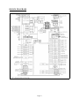
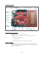
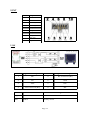
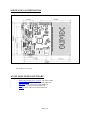
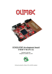
STM32-P107 development board
User's Manual
All boards produced by Olimex are ROHS compliant
Rev. F, August 2012
Copyright(c) 2012, OLIMEX Ltd, All rights reserved
Page 1
INTRODUCTION
STM32-P107 prototype board provides easy way for developing and prototyping
with the new STM32F107VCT6 connectivity line microcontroller, produced by
STMicroelectronics. STM32-P107 has JTAG port for programming and debugging,
USB_OTG, user button, two status leds, and most of the GPIOs are on extension
headers where you can connect your additional circuits.
BOARD FEATURES
-
CPU: STM32F107VCT6 32 bit ARM-based microcontroller with 256 KB Flash, 64
KB RAM, USB OTG, Ethernet, 10 timers, 2 CANs, 2 ADCs, 14 communication
interfaces
-
JTAG connector with ARM 2x10 pin layout for programming/debugging
-
USB_OTG
-
USB_HOST
-
100Mbit Ethernet
-
RS232
-
Mini SD/MMC card connector
-
UEXT connector
-
Power Jack
-
Two user buttons
-
RESET button and circuit
-
Two status leds
-
Power-on led
-
3V battery connector
-
Extension port connectors for many of microcontrollers pins
-
PCB: FR-4, 1.5 mm (0,062"), soldermask, silkscreen component print
-
Dimensions: 132.08x96.52mm (5.2x3.8")
ELECTROSTATIC WARNING
The STM32-P107 board is shipped in protective anti-static packaging. The board
must not be subject to high electrostatic potentials. General practice for working
with static sensitive devices should be applied when working with this board.
Page 2
BOARD USE REQUIREMENTS
Cables: The cable you will need depends on the programmer/debugger you use. If
you use ARM-JTAG, you will need LPT cable, if you use ARM-JTAG-EW, ARMUSB-OCD, ARM-USB-OCD-H, ARM-USB-TINY, or ARM-USB-TINY-H you will
need 1.8 meter USB A-B cable, for ARM-USB-OCD and ARM-USB-OCD-H you will
need RS232 cable, too.
Hardware: Programmer/Debugger – one of the Olimex ARM Programmers: ARMJTAG, ARM-JTAG-EW, ARM-USB-OCD, ARM-USB-OCD-H, ARM-USB-OCDTINY, ARM-USB-OCD-H.
Software: ARM C compiler
PROCESSOR FEATURES
STM32-P107 board use ARM-based 32-bit microcontroller STM32F107VCT6 with
these features:
–
–
–
–
–
Core: ARM 32-bit Cortex™-M3 CPU
–
72 MHz maximum frequency, 1.25 DMIPS/MHz (Dhrystone 2.1)
performance at 0 wait state memory access
–
Single-cycle multiplication and hardware division
Memories
–
256 Kbytes of Flash memory
–
64 Kbytes of SRAM
Clock, reset and supply management
–
2.0 to 3.6 V application supply and I/Os
–
POR, PDR, and programmable voltage detector (PVD)
–
25 MHz crystal oscillator
–
Internal 8 MHz factory-trimmed RC
–
Internal 40 kHz RC with calibration
–
32 kHz oscillator for RTC with calibration
Low power
–
Sleep, Stop and Standby modes
–
VBAT supply for RTC and backup registers
2 × 12-bit, 1 µs A/D converters (16 channels)
–
Conversion range: 0 to 3.6 V
–
Sample and hold capability
–
Temperature sensor
–
up to 2 MSps in interleaved mode
–
2 × 12-bit D/A converters
–
DMA: 12-channel DMA controller
Page 3
–
–
–
Debug mode
–
Serial wire debug (SWD) & JTAG interfaces
–
Cortex-M3 Embedded Trace Macrocell™
80 fast I/O ports
–
–
–
–
Supported peripherals: timers, ADCs, DAC, I2Ss, SPIs, I2Cs and
USARTs
80 I/Os, all mappable on 16 external interrupt vectors and almost all 5
V-tolerant
10 timers
–
four 16-bit timers, each with up to 4 IC/OC/PWM or pulse counter and
quadrature (incremental) encoder input
–
1 × 16-bit motor control PWM timer with dead-time generation and
emergency stop
–
2 × watchdog timers (Independent and Window)
–
SysTick timer: a 24-bit downcounter
–
2 × 16-bit basic timers to drive the DAC
14 communication interfaces
–
2 × I2C interfaces (SMBus/PMBus)
–
5 USARTs (ISO 7816 interface, LIN, IrDA capability, modem control)
–
3 SPIs (18 Mbit/s), 2 with a multiplexed I2S interface that offers audio
class accuracy via advanced PLL schemes
–
2 × CAN interfaces (2.0B Active) with 512 bytes of dedicated SRAM
–
USB 2.0 full-speed device/host/OTG controller with on-chip PHY that
supports HNP/SRP/ID with 1.25 Kbytes of dedicated SRAM
–
10/100 Ethernet MAC with dedicated DMA and SRAM (4 Kbytes):
IEEE1588 hardware support, MII/RMII available on all packages
CRC calculation unit, 96-bit unique ID
Page 4
BLOCK DIAGRAM
Page 5
MEMORY MAP
Page 6
SCHEMATIC
97
98
1
2
3
4
5
38
39
40
41
42
43
44
45
46
ETH_RMII_MDINT
USB_FAULT
PE0/TIM4_ETR
PE1
PE2/TRACECK
PE3/TRACED0
PE4/TRACED1
PE5/TRACED2
PE6/TRACED3
PE7/TIM1_ETR
PE8/TIM1_CH1N
PE9/TIM1_CH1
PE10/TIM1_CH2N
PE11/TIM1_CH2
PE12/TIM1_CH3N
PE13/TIM1_CH3
PE14/TIM1_CH4
PE15/TIM1_BKIN
PD0/OSC_IN/CAN1_RX
PD1/OSC_OUT/CAN1_TX
PD2/TIM3_ETR/UART5_RX
PD3/USART2_CTS
PD4/USART2_RTS
PD5/USART2_TX
PD6/USART2_RX
PD7/USART2_CK
PD8/USART3_TX/ETH_MII_RX_DV
PD9/USART3_RX/ETH_MII_RX_D0
PD10/USART3_CK/ETH_MII_RX_D1
PD11/USART3_CTS/ETH_MII_RX_D2
PD12/TIM4_CH1/USART3_RTS/ETH_MII_RX_D3
PD13/TIM4_CH2
PD14/TIM4_CH3
PD15/TIM4_CH4
81
82
83
84
85
86
87
88
55
56
57
58
59
60
61
62
SPI3_SCK
SPI3_MISO
SPI3_MOSI
TAMPER
SPI3_SCK
SPI3_MISO
SPI3_MOSI
GN D
C14
10pF
C15
10pF
JTAG
1
2
HN1x2(Open)
3.3V
U3
RM3G1
TDO
RST
TRST
1
R-T
R26
330R
D5
BOOT0_E
1
2
BOOT0
HN1x2(Open)
12
9
R1OUT
R2OUT
3.3V
13 PC_TXD
8 PC_CTS
R1IN
R2IN
16VCC
GND15
U3PWR
C29
100nF
1N4148
1
2
3
4
5
R30
6
7
8
9
R27
NA
TAMPER
TAMPER
330R
R29
100R/1%
R36
R37
NA
WKUP
330R
3.3V
NA(33k)
POWER SUPPLY CIRCUIT
VDD
E/D
1N5819S
+5V_EXT
D4
1N5819S
VR2(3.3V)
LM1117IMPX-ADJ
IN
1
C9
C10
2.2uF/6.3V
+
47uF/6.3V/TANT
C7
+
C6
100nF
47uF/6.3V/TANT
C4
24 0R/1%
2
R9
3 90R/1 %
C8
N A (1 0 u F /6 .3 V )
R7
300R/1%
100nF
GND
100nF
ETH_RMII_REF_CLK
R50
4.99k/1%
R49
1.5k/1%
36
35
34
33
32
31
1k
30
29
NA
28
27 330R
26 330R
330R
25
R47
R46
R45
R44
USB
GND3
GND4
R5
R4
SPI3_SCK
SPI3_MISO
SPI3_MISO
33k
33k
33k
R3
R2
R1
L3
CL470 nH/08 05/1.7 6R/250 mA
C40
47uF/6.3V/TANT
LAN
LAN
1
3
2
AG
KG
AY
KY
7
6
8
10k
R43
TD+
COM
TDAG
KG
AY
KY
RD+
NC
RD-
1:1
75
U2
YEL LOW
1:1
75
R48
3.3V
3.3V
3.3V
C48
100nF
R61
10k
STAT1
STAT2
NA(STM1001RWX6F)
2 VCC RESET 1
R62
330R
R63
100R/1%
GND
1
2
AGND
GREEN(GYX-SD-TC0805SGC)
YELLOW(GYX-SD-TC0805SYC)
RESET
3
7
8
6
R58
4.7k
3.3V
UEXT
UEXT_PWR_E
CLOSE
UEXT
USART3_TX
I2C1_SCL
SPI3_MISO
SPI3_SCK
1
3
5
7
9
2
4
6
8
10
R59
4.7k
USART3_RX
I2C1_SDA
SPI3_MOSI
CS_UEXT
BH10S
3.3V
PB2/BOOT1
R64
10k
R57
330R
75
1nF/2 kV
1
4
5
2
RJLBC-060TC1
3.3V
KS8721BLMM
RESET CIRCUIT
3.3V
75
GRE EN
3.3V
3.3V
GNDA_E
CLOSE
GND1
GND2
C36
C35
100nF C37
10uF/6.3V
100nF
10k
33k
1.5k/1%
R21
1
2
3
R22
1M
10k
3.3V
10uF/6.3V
GND5
GND4
FXSD/FXEN
RX+
RXVDDRX
PD#
LED3/NWAYEN
LED2/DUPLEX
LED1/SPD100/NFEF
LED0/TEST
INT/PHYAD0
3
100nF
C3
C49
U4
R56
330R
C2
100nF
100nF
L5
MDIO
MDC
RXD3/PHYAD1
RXD2/PHYAD2
RXD1/PHYAD3
RXD0/PHYAD4
VDDIO1
GND1
RXDV/CRSDV/PCS_LPBK
RXC
RXER/ISO
GND2
OUT
CLOSE
C11
R8
C44
C43
STAT2
STAT1
3.3VA_E
OUT
ADJ/GND
+
10uF/6.3V
STATUS LEDS
2
D3
CS_MMC
SPI3_MOSI
3.3VA
1
+5V_OTG_PWR
3.3V_E
CLOSE
MICRO
3.3V
CS_MMC
SPI3_MOSI
SPI3_SCK,SPI3_MOSI,SPI3_MISO,CS_UEXT,I2C1_SCL,I2C1_SDA,USART3_TX,USART3_RX,SPI1_NSS,SPI1_SCK,SPI1_MISO,SPI1_MOSI,USART2_TX,USART2_RX,USART2_RTS,USART2_CTS
3.3V
330R
PWR_LED
RED(GYX-SD-TC0805SYRK)
C5
GND_PIN
2
R6
100R/1%
NA(10uF/6.3V)
C1
470uF/16VDC
+
6VAC
(6.5-9)VDC
VO
GND/ADJ
1N5819S
47uF/6.3V/TANT
VI
1
3
YDJ-1136
D2
2
3
6
4
5
7
8
1
CD/DAT3/CS
CMD/DI
VSS
VDD
CLK/SCLK
DAT0/DO
DAT1/RES
DAT2/RES
2
4
6
8
10
12
14
16
18
20
3.3VA
R10
+5V_JTAG
VSS
C50
1
NA(6NC2-50MHz)
+5V
PWR_JACK
1
2
3
4
5
6
7
8
9
10
11
12
R41
CD1
2
VR1(5.0V)
AME1085
10k
R39
ETH_RXER
R34
R35
0R(NA)
NA
3.3V
1k
3
G1
0R
R38
R32
100R/1%
3.3V
1
3
5
7
9
11
13
15
17
19
PHY_VDD_PLL
PHY_RSTN
ETH_RMII_CRS_DV
C31
100nF
4
DB 104(S M D)
10k
ETH_RMII_RXD1
ETH_RMII_RXD0
R31
33k
+5V
+5V_JTAG
FB0805/600R/200mA(201209-601)
C41
100nF
C42
10uF/6.3V
R33
C30
100nF
MICRO_AB
2.5V
1k
1k
1k
1k
47k
1N4148 D6
WKUP
L1
FB0805/600R/200mA(201209-601)
BH20S
3.3V
R28
10k
RS232
PC_DCD
14 PC_RXD
7 PC_RTS
T1OUT
T2OUT
10k
10k
SD/MMC
JTAG
OPEN
ETH_RMII_MDIO
ETH_RMII_MDC
T1103NE-DTSM-21R(12x12x4.3mm)
T1IN
T2IN
RM4G3
RM4G4
2
RM1G1
RM1G2
RM1G3
RM1G4
USART2_RX
USART2_CTS
C2-
11
10
10k
3.3V
3.3V
T1103NE-DTSM-21R(12x12x4.3mm)
R25
330R
R65
C2+
5
USART2_TX
USART2_RTS
6
V-
DTC114YKA
C26
4
100nF
10k RM4G1
10k
C28
100nF
C27
100nF
2
V+
C1-
1k
C1+
3
C39
100nF
USART3_TX
USART3_RX
T2
ST3232BDR(SO16)
C25
1
100nF
C38
2.2uF/6.3V
USB_OTG
VBUS
DD+
ID
GND
SD/MMC
3.3V
RM4G2 RM3G2 RM3G3 RM3G4
10k
10k
10k
10k
R24
NA
TRST
TDI
TMS
TCK
USART2_CTS
USART2_RTS
USART2_TX
USART2_RX
BUTTONS
RST_E
1
2
3
1
2
3
ETH_RMII_RXD0
ETH_RMII_RXD1
RST
PHY_SOFT_RST
RST
+5V_OTG_PWR
USB_OTG_DUSB_OTG_D+
OTG_ID
OTG_ID
STM32F107VCT6
RS232
USB_OTG
+5V_OTG_PWR
USB_OTG_DUSB_OTG_D+
USB_HOST_DUSB_OTG_D-
RJ45 SIDE
NRST
NC
3.3V
0
1
1
2
3
PE0
PE1
PE2
PE3
PE4
PE5
PE6
PE7
PE8
PE9
PE10
PE11
PE12
PE13
14
73
33k
100nF C47
RST
RST
ETH_RMII_MDC
PC6
PC7
PC8
PC9
PC10
PC11
PC12
PC13
Q2
NA
32768Hz/6pF
R16
PD0
PD1
PD2
USART2_CTS
PD3
USART2_RTS
PD4
USART2_TX
PD5
USART2_RX
PD6
USB_VBUSON
USART3_TX
PD8
USART3_RX
PD9
PD10
PD11
PD12
ETH_RXER
PD13
PHY_SOFT_RST
PD14
PD15
H
100nF C46
OSC_OUT
NA(47pF)
100nF
O
+
OSC_IN
13
150R
NA (US BLC6-2P6)
49.9R/1%
49.9R/1%
49.9R/1%
NA
49.9R/1%
R15
C34
SHIELD
USB_A
FB0805/600R/200mA(201209-601)
CS_UEXT
PC2
PC3
ETH_RMII_RXD0
ETH_RMII_RXD1
STAT1
STAT2
C33
LM3526-L
R23
USB_DHN1x3(O:Close,H:Open)
ETH_RMII_TX_EN
ETH_RMII_TXD0
ETH_RMII_TXD1
PC0
ETH_RMII_MDC
1
2
3
R51
R52
R53
R54
R55
R14
NA
Q1
Q25.000MHz/HC-49SM(SMD)/20pF
C13
27pF
12
15
16
17
18
33
34
63
64
65
66
78
79
80
7
8
9
C32
6
5
4
LED100/DUP
LEDACT
B0_0/B0_1
PC0/ADC12_IN10
PC1/ADC12_IN11/ETH_MII_MDC/ETH_RMII_MDC
PC2/ADC12_IN12/ETH_MII_TXD2
PC3/ADC12_IN13/ETH_MII_TX_CLK
PC4/ADC12_IN14/ETH_MII_RXD0/ETH_RMII_RXD0
PC5/ADC12_IN15/ETH_MII_RXD1/ETH_RMII_RXD1
PC6/I2S2_MCK/TIM3_CH1
PC7/I2S3_MCK/TIM3_CH2
PC8/TIM3_CH3
PC9/TIM3_CH4
PC10/UART4_TX/USART3_TX/SPI3_SCK
PC11/UART4_RX/USART3_RX/SPI3_MISO
PC12/UART5_TX/USART3_CK/SPI3_MOSI
PC13/TAMPER-RTC
PC14/OSC32_IN
PC15/OSC32_OUT
BOOT0
R20
100nF C45
94
R19
22R
8
#ENA
OUT_A 7
FLAG_A
IN 6
FLAG_B
GND 5
#ENB
OUT_B
2
1
2
3
C12
27pF
10k
1
22R
OTG_DM
NA(47pF)
I2C1_SCL
I2C1_SDA
PB14
PB15
CS_UEXT
OTG_DP
1
2
3
4
1
R13
HN1x3
0
VBAT
ETH_RMII_TX_EN
ETH_RMII_TXD0
ETH_RMII_TXD1
USB_FAULT
U6
PB0
PB1
PB2TDO
TRST
PB5
PB6
PB7
PB8
PB9
PB10
I2C1_SCL
I2C1_SDA
USB_VBUSON
USB_HOST_D+
USB_OTG_D+
3.3V
47k
+5V
U5
DTA114YKA
ETH_RMII_MDINT
1
2
6
H
T1107A(6x3,8x2,5mm)
BOOT0
D1
BAT54C
3V_BAT
WF2S
TMS
TCK
TDI
T1
3.3V
ETH_RMII_REF_CLK
ETH_RMII_TX_EN
ETH_RMII_TXD0
ETH_RMII_TXD1
RM2G1
1k
RM2G2
1k
RM2G3
1k
RM2G4
1k
3.3V
4
USB_D+
HN1x3(O:Close,H:Open)
O
PB2/BOOT1
TDO
TRST
USB_HOST
+5V_HOST_PWR 1
USB_HOST_D2
USB_HOST_D+
3
L2
ETH_RMII_CRS_DV
48
47
46
45
44
43
42
41
40
39
38
37
VREF-
VREFVBAT
CS_MMC
33R
3.3V
VREF+
20
0R(NA)
+5V_HOST_PWR
USB_HOST_DUSB_HOST_D+
RST#
VDDPLL
XI
XO
GND8
GND7
VDDTX
TX+
TXGND6
VDDRCV
REXT
21
ETH_RMII_CRS_DV
R17
OTG_VBUS
OTG_ID
OTG_DM
OTG_DP
TMS
TCK
+5V_HOST_PWR
+5V_OTG_PWR
VDDC
TXER
TXC/REFCLK
TXEN
TXD0
TXD1
TXD2
TXD3
COL/RMII
CRS/RMII_BTB
GND3
VDDIO2
NA
CS_MMC
USB_HOST
H
1k
100nF
C24
PA3
PA4
PA5
PA6
O
0R
1k
0R(NA)
C23
ETH_RMII_REF_CLK
ETH_RMII_MDIO
13
14
15
16
17
18
19
20
21
22
23
24
VSSA
35
36
37
89
90
91
92
93
95
96
47
48
51
52
53
54
PA0
L6
19
PB0/ADC12_IN8/TIM3_CH3/ETH_MII_RXD2/TIM1_CH2N
PB1/ADC12_IN9/TIM3_CH4/ETH_MII_RXD3/TIM1_CH3N
PB2/BOOT1
PB3/JTDO/SPI3_SCK/TRACESWO/TIM2_CH2/SPI1_SCK
PB4/JNTRST/SPI3_MISO/TIM3_CH1/SPI1_MISO
PB5/I2C1_SMBAL/SPI3_MOSI/ETH_MII_PPS_OUT/ETH_RMII_PPS_OUT/TIM3_CH2/SPI1_MOSI/CAN2_RX
PB6/I2C1_SCL/TIM4_CH1/USART1_TX/CAN2_TX
PB7/I2C1_SDA/TIM4_CH2/USART1_RX
PB8/TIM4_CH3/ETH_MII_TXD3/I2C1_SCL/CAN1_RX
PB9/TIM4_CH4/I2C1_SDA/CAN1_TX
PB10/I2C2_SCL/USART3_TX/ETH_MII_RX_ER/TIM2_CH3
PB11/I2C2_SDA/USART3_RX/ETH_MII_TX_EN/ETH_RMII_TX_EN/TIM2_CH4
PB12/SPI2_NSS/I2S2_WS/I2C2_SMBAL/USART3_CK/TIM1_BKIN/CAN2_RX/ETH_MII_TXD0/ETH_RMII_TXD0
PB13/SPI2_SCK/I2S2_CK/USART3_CTS/TIM1_CH1N/CAN2_TX/ETH_MII_TXD1/ETH_RMII_TXD1
PB14/SPI2_MISO/TIM1_CH2N/USART3_RTS
PB15/SPI2_MOSI/I2S2_SD/TIM1_CH3N
WKUP
ETH_RMII_REF_CLK
ETH_RMII_MDIO
R42
VDDA
VREF+
33R
0R
C22
100nF
23
24
25
26
29
30
31
32
67
68
69
70
71
72
76
77
R40
C21
10uF/6.3V
R12
VSS
VSS
VSS
VSS
VSS
22
F B0805/ 600R/ 200mA(201209-601)
PA0/WKUP/USART2_CTS/ADC12_IN0/TIM2_CH1_ETR/TIM5_CH1/ETH_MII_CRS_WKUP
PA1/USART2_RTS/ADC12_IN1/TIM5_CH2/TIM2_CH2/ETH_MII_RX_CLK/ETH_RMII_REF_CLK
PA2/USART2_TX/TIM5_CH3/ADC12_IN2/TIM2_CH3/ETH_MII_MDIO/ETH_RMII_MDIO
PA3/USART2_RX/TIM5_CH4/ADC12_IN3/TIM2_CH4/ETH_MII_COL
PA4/SPI1_NSS/DAC_OUT1/USART2_CK/ADC12_IN4
PA5/SPI1_SCK/DAC_OUT2/ADC12_IN5
PA6/SPI1_MISO/ADC12_IN6/TIM3_CH1/TIM1_BKIN
PA7/SPI1_MOSI/ADC12_IN7/TIM3_CH2/ETH_MII_RX_DV/ETH_RMII_CRS_DV/TIM1_CH1N
PA8/USART1_CK/OTG_FS_SOF/TIM1_CH1/MCO
PA9/USART1_TX/TIM1_CH2/OTG_FS_VBUS
PA10/USART1_RX/TIM1_CH3/OTG_FS_ID
PA11/USART1_CTS/CAN1_RX/TIM1_CH4/OTG_FS_DM
PA12/USART1_RTS/CAN1_TX/TIM1_ETR/OTG_FS_DP
PA13/JTMS/SWDIO
PA14/JTCK/SWCLK
PA15/JTDI/SPI3_NSS/TIM2_CH1_ETR/SPI1_NSS
R18
OTG_VBUS
C51 100nF
100nF C20
100nF C19
100nF C18
L4
R11
VDD
VDD
VDD
VDD
VDD
10
27
99
74
49
3.3V
2
1
CLOSE
3.3VA_MCU_E
3.3VA
100nF C17
100nF C16
50
75
100
28
11
USB CIRCUIT
VBUS
HN1x3(O:Close,H:Open)
U1
FB0805/600R/200mA(201209-601)
1
2
3.3V_MCU_E
CLOSE
USB
STM32-P107_rev_B
OLIMEX LTD BULGARIA
www.olimex.com
3.3V
C52
100nF
RST
B1_0/B1_1
HN1x3
R60
33k
BOARD LAYOUT
POWER SUPPLY CIRCUIT
STM32-P107 can take power from three sources:
–
PWR connector where (6.5-9)V DC or 6V AC is applied by external power
source.
–
+5V_ OTG-PWR from USB OTG
–
+5V_JTAG from JTAG
The programmed board power consumption is about 70 mA.
RESET CIRCUIT
STM32-P107 reset circuit includes JTAG connector pin 15, U2 (STE101P) pin 28
(RESET), R73(10k), R74(330Ohm), R75(100Ohm/1%), C55(100nF), STM32F107 pin
14 (NRST) and RESET button.
Page 8
CLOCK CIRCUIT
Quartz crystal 25 MHz is connected to STM32F107 pin 12 (OSC_IN) and pin
13 (OSC_OUT).
Quartz crystal 32.768kHz is connected to STM32F107 pin 8
(PC14/OSC32_IN) and pin 9 (PC15/OSC32_OUT).
JUMPER DESCRIPTION
PWR_SEL
When position 1-2 is shorted – the board is power supplied from JTAG.
When position 3-4 is shorted – the board is power supplied from USB_OTG.
When position 5-6 is shorted – the board is power supplied from External power
source.
Default state is – position 5-6 – shorted.
B0_0/B0_1
When this jumper is in position B0_1 – BOOT0 is connected to 3.3V, and when the
jumper is in position B0_0 – BOOT0 is connected to GND.
Default state is B0_0.
B1_0/B1_1
When this jumper is in position B1_1 – BOOT1 is connected to 3.3V, and when the
jumper is in position B1_0 – BOOT1 is connected to GND.
Default state is B1_0.
VBUS
When is in position “H” - connects +5V_HOST_PWR to OTG_VBUS.
When is in position “O” - connects +5V_OTG_PWR to OTG_VBUS.
Default state is “O”.
USB_D+
When is in position “H” - connects USB_HOST_D+ to OTG_DP.
When is in position “O” - connects USB_OTG_D+ to OTG_DP.
Default state is “O”.
USB_DWhen is in position “H” - connects USD_HOST_D- to OTG_DM.
When is in position “O” - connects USB_OTG_D- to OTG_DM.
Default state is “O”.
PWDW_D
When is closed – disables Ethernet transceiver (STE101P) Power Down Mode.
STE101P is active.
Default state is closed.
Page 9
3.3V_MCU_E
Enable microcontroller 3.3V power supply
Default state is closed.
3.3V_E
Enable regulator VR2 (3.3V) - LM1117
Default state is closed.
3.3VA_E
Enables board 3.3V analog power supply.
Default state is closed.
3.3VA_MCU_E
Enables microcontroller 3.3V analog power supply.
Default state is closed.
GNDA_E
Enables board analog GND.
Default state is closed.
R-T
Connects RST to TRST
Default state is open.
RST_E, BOOT_E jumpers
Note that it is recommended to move those jumpers together – either both should be
open or both should be closed.
When both are closed RS232 boot is enabled.
Default states are RST_E – open; BOOT_E – open.
INPUT/OUTPUT
Status LED1 (green) with name STAT1 connected to STM32F107 pin 63
(PC6/I2S2_MCK/TIM3_CH1).
Status LED2 (yellow) with name STAT2 connected to STM32F107 pin 64
(PC7/I2S3_MCK/TIM3_CH2).
Power-on LED (red) with name PWR – this led shows that +3.3V is applied to the
board.
User button with name WKUP connected to STM32F107 pin 23 (PA0/WKUP).
User button with name TAMPER connected to STM32F107 pin 7 (PC13/TAMPERRTC).
Reset button with name RESET connected to STM32F107 pin 14 (NRST).
Page 10
CONNECTOR DESCRIPTIONS
JTAG
The JTAG connector allows the software debugger to talk via a JTAG (Joint Test
Action Group) port directly to the core. Instructions may be inserted and executed by
the core thus allowing STM32F107 memory to be programmed with code and
executed step by step by the host software.
For more details refer to IEEE Standard 1149.1 - 1990 Standard Test Access Port and
Boundary Scan Architecture and STM32F107 datasheets and users manual.
Pin #
Signal Name
Pin #
Signal Name
1
3.3V
2
3.3V
3
TRST
4
GND
5
TDI
6
GND
7
TMS
8
GND
9
TCK
10
GND
11
PULL-DOWN
12
GND
13
TDO
14
GND
15
RST
16
GND
17
PULL-DOWN
18
GND
19
+5V_JTAG
20
GND
PWR_JACK
Pin #
Signal Name
1
Power Input
2
GND
Page 11
USB_HOST
Pin #
Signal Name
1
+5V_HOST_PWR
2
USB_HOST_D-
3
USB_HOST_D+
4
GND
USB_OTG
Pin #
Signal Name
1
+5V_OTG_PWR
2
USB_OTG_D-
3
USB_OTG_D+
4
OTG_ID
5
GND
3V_BAT
Pin #
Signal Name
1
VBAT
2
GND
Page 12
RS232
The RS232 port can be used for communication when in bootloader mode. To enter bootloader mode
you need to close RST_E and BOOT0_E jumpers. Note that the default position of those jumpers is
closed, e.g. bootloader mode disabled.
Pin #
Signal Name
1
NC
2
T1OUT
3
R1IN
4
NC
5
GND
6
NC
7
CTS
8
RTS
9
NC
Page 13
UEXT
Pin #
Signal Name
1
3.3V
2
GND
3
USART2_TX
4
USART2_RX
5
I2C1_SCL
6
I2C1_SDA
7
SPI3_MISO
8
SPI3_MOSI
9
SPI3_SCK
10
CS_UEXT
LAN
Pin #
Signal Name Chip Side
Pin #
Signal Name Chip Side
1
TX+
5
Not Connected (NC)
2
TX-
6
VDD
3
VDD
7
RX+
4
Not Connected (NC)
8
RX-
LED
Color
Usage
Right
Green
Link status
Left
Yellow
Activity status
Page 14
SD/MMC
Pin #
Signal Name
1
MCIDAT2
2
CS_MMC
3
SPI3_MOSI
4
3.3V
5
SPI3_SCK
6
GND
7
SPI3_MISO
8
MCIDAT1
9
Not connected
10
Not connected
11
Not connected
12
Not connected
Page 15
MECHANICAL DIMENSIONS
All measures are in mils.
AVAILABLE DEMO SOFTWARE
–
–
–
–
–
NEW STM32-P107 demo package with Micrel PHY
Blinking LED Demo software for EW-ARM 5.50
Ethernet Demo software for EW-ARM 5.50
USB Demo software for EW-ARM 5.50
SD card Demo software for EW-ARM 5.50
Page 16
ORDER CODE
STM32-P107 – assembled and tested
How to order?
You can order to us directly or by any of our distributors.
Check our web www.olimex.com/dev for more info.
Manual revision history:
REV. Initial
- created December 2009
REV. A
- edited by TU December 2010
REV. B
- demo software added and mechanical dimensions detailed
REV. C
- Rev. A schematic and added more programmers in BOARD USE REQUIREMENTS.
REV. D
- edited June 2011 – changed schematic
REV. E
- changed schematics to rev. B, added board revision history
REV.F
- added BOOT0_E, RST_E description, changed dimensions, updated revision B
pictures, updated disclaimer
Board revision history:
rev.A
========
1. ST2052BD is exchanged with LM3526-L.
2. SD/MMC signals are changed as follows:
SPI1_MOSI
->
SPI3_MOSI
SPI1_SCK
->
SPI3_SCK
SPI1_MISO
->
SPI3_MISO
and SPI1_NSS renamed to CS_MMC
3. Changed the polarity to + of C36
In Rev.B
========
1. All libraries are updated
2. Ethernet PHY is changed from STE101P to MICREL's one - KS8721BLMM
3. All 10uF/6.3V/TANT are changed to 0805 and a lot of element names are changed.
4. PWR_SEL jumpers are replaced by diodes.
5. USART3 is connected to UEXT while USART2 is connected to RS232 and bootloader functionality is enabled!
Two additional jumpers are added!!!
6. Added UEXT_PWR_E jumper!
7. A lot jumpers are added into jumpers description table
Page 17
© 2012 Olimex Ltd. Olimex®, logo and combinations thereof, are registered trademarks of Olimex Ltd. Other product names
may be trademarks of others and the rights belong to their respective owners.
The information in this document is provided in connection with Olimex products. No license,
express or implied or otherwise, to any intellectual property right is granted by this document
or in connection with the sale of Olimex products.
The hardware files are closed source. Routing schematics and bill of materials are kept privite. You
may NOT reproduce the design for commercial use. You may modify the design, but you must then
release a link to the creator website: http://www.olimex.com.
The software is released under GPL.
It is possible that the pictures in this manual differ from the latest revision of the board.
The product described in this document is subject to continuous development and improvements. All
particulars of the product and its use contained in this document are given by OLIMEX in good faith.
However all warranties implied or expressed including but not limited to implied warranties of
merchantability or fitness for purpose are excluded. This document is intended only to assist the
reader in the use of the product. OLIMEX Ltd. shall not be liable for any loss or damage arising from
the use of any information in this document or any error or omission in such information or any
incorrect use of the product.
This evaluation board/kit is intended for use for engineering development, demonstration, or
evaluation purposes only and is not considered by OLIMEX to be a finished end-product fit for general
consumer use. Persons handling the product must have electronics training and observe good
engineering practice standards. As such, the goods being provided are not intended to be complete in
terms of required design-, marketing-, and/or manufacturing-related protective considerations,
including product safety and environmental measures typically found in end products that incorporate
such semiconductor components or circuit boards.
Olimex currently deals with a variety of customers for products, and therefore our arrangement with
the user is not exclusive. Olimex assumes no liability for applications assistance, customer product
design, software performance, or infringement of patents or services described herein.
THERE IS NO WARRANTY FOR THE DESIGN MATERIALS AND THE COMPONENTS USED TO CREATE
STM32-P107. THEY ARE CONSIDERED SUITABLE ONLY FOR STM32-P107.
Page 18