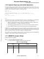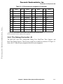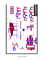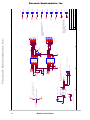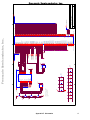
1
Freescale Semiconductor, Inc...
Freescale Semiconductor, Inc.
M5407C3 User's Manual
M5407C3UM/D
Rev. 1.1, 8/2000
Freescale Semiconductor, Inc.
How to Reach Us:
Home Page:
www.freescale.com
Freescale Semiconductor, Inc...
E-mail:
[email protected]
USA/Europe or Locations Not Listed:
Freescale Semiconductor
Technical Information Center, CH370
1300 N. Alma School Road
Chandler, Arizona 85224
+1-800-521-6274 or +1-480-768-2130
[email protected]
Europe, Middle East, and Africa:
Freescale Halbleiter Deutschland GmbH
Technical Information Center
Schatzbogen 7
81829 Muenchen, Germany
+44 1296 380 456 (English)
+46 8 52200080 (English)
+49 89 92103 559 (German)
+33 1 69 35 48 48 (French)
[email protected]
Japan:
Freescale Semiconductor Japan Ltd.
Headquarters
ARCO Tower 15F
1-8-1, Shimo-Meguro, Meguro-ku,
Tokyo 153-0064
Japan
0120 191014 or +81 3 5437 9125
[email protected]
Asia/Pacific:
Freescale Semiconductor Hong Kong Ltd.
Technical Information Center
2 Dai King Street
Tai Po Industrial Estate
Tai Po, N.T., Hong Kong
+800 2666 8080
[email protected]
For Literature Requests Only:
Freescale Semiconductor Literature Distribution Center
P.O. Box 5405
Denver, Colorado 80217
1-800-441-2447 or 303-675-2140
Fax: 303-675-2150
[email protected]
Information in this document is provided solely to enable system and software
implementers to use Freescale Semiconductor products. There are no express or
implied copyright licenses granted hereunder to design or fabricate any integrated
circuits or integrated circuits based on the information in this document.
Freescale Semiconductor reserves the right to make changes without further notice to
any products herein. Freescale Semiconductor makes no warranty, representation or
guarantee regarding the suitability of its products for any particular purpose, nor does
Freescale Semiconductor assume any liability arising out of the application or use of
any product or circuit, and specifically disclaims any and all liability, including without
limitation consequential or incidental damages. “Typical” parameters which may be
provided in Freescale Semiconductor data sheets and/or specifications can and do
vary in different applications and actual performance may vary over time. All operating
parameters, including “Typicals” must be validated for each customer application by
customer’s technical experts. Freescale Semiconductor does not convey any license
under its patent rights nor the rights of others. Freescale Semiconductor products are
not designed, intended, or authorized for use as components in systems intended for
surgical implant into the body, or other applications intended to support or sustain life,
or for any other application in which the failure of the Freescale Semiconductor product
could create a situation where personal injury or death may occur. Should Buyer
purchase or use Freescale Semiconductor products for any such unintended or
unauthorized application, Buyer shall indemnify and hold Freescale Semiconductor
and its officers, employees, subsidiaries, affiliates, and distributors harmless against all
claims, costs, damages, and expenses, and reasonable attorney fees arising out of,
directly or indirectly, any claim of personal injury or death associated with such
unintended or unauthorized use, even if such claim alleges that Freescale
Semiconductor was negligent regarding the design or manufacture of the part.
© Motorola Inc., 2000. All rights reserved.
Freescale Semiconductor, Inc.
LIMITED WARRANTY
Freescale Semiconductor, Inc...
Matrix Design warrants this product against defects in material and workmanship for
a period of sixty (60) days from the original date of purchase. This warranty extends
to the original customer only and is in lieu of all other warrants, including
implied warranties of merchantability and fitness. In no event will the seller be
liable for any incidental or consequential damages. During the warranty period,
Matrix Design will replace, at no charge, components that fail, provided the product
is returned (properly packed and shipped prepaid) to Matrix Design at address below.
Dated proof of purchase (such as a copy of the invoice) must be enclosed with the
shipment. We will return the shipment prepaid via UPS.
This warranty does not apply if, in the opinion of Matrix Design, the product has been
damaged by accident, misuse, neglect, misapplication, or as a result of service or
modification (other than specified in the manual) by others.
Please send the board and cables with a complete description of the problem to:
Matrix Design & Manufacturing, Inc.
2914 Montopolis Drive #290
Austin, TX 78741
Phone: (512) 385-9210
Fax: (512) 385-9224
http://www.cadreiii.com
Freescale Semiconductor, Inc.
WARNING
Freescale Semiconductor, Inc...
This board generates, uses, and can radiate radio frequency energy and, if not installed
properly, may cause interference to radio communications. As temporarily permitted
by regulation, it has not been tested for compliance with the limits for class a
computing devices pursuant to Subpart J of Part 15 of FCC rules, which are designed
to provide reasonable protection against such interference. Operation of this product
in a residential area is likely to cause interference, in which case the user, at his/her
own expense, will be required to correct the interference.
Freescale Semiconductor, Inc.
apps docs:ColdFire:5407:Eval Board UM NEW:5407C3UMTOC.fm
8/14/00
CONTENTS
Paragraph
Number
Page
Number
Title
Freescale Semiconductor, Inc...
Chapter 1
M5407C3 Board
1.1
1.2
1.3
1.4
1.5
1.6
1.7
1.8
1.9
1.9.1
1.9.2
1.9.3
1.9.4
1.9.5
1.9.6
1.9.7
1.10
1.11
1.12
General Hardware Description ........................................................................... 1-1
System Memory .................................................................................................. 1-4
Serial Communication Channels......................................................................... 1-4
Parallel I/O Ports................................................................................................. 1-4
Programmable Timer/Counter ............................................................................ 1-5
PCI Controller..................................................................................................... 1-5
On Board Ethernet .............................................................................................. 1-5
System Configuration ......................................................................................... 1-5
Installation And Setup......................................................................................... 1-7
Unpacking....................................................................................................... 1-7
Preparing the Board for Use ........................................................................... 1-7
Providing Power to the Board......................................................................... 1-8
Selecting Terminal Baud Rate ........................................................................ 1-8
The Terminal Character Format ..................................................................... 1-8
Connecting the Terminal ................................................................................ 1-8
Using a Personal Computer as a Terminal...................................................... 1-8
System Power-up and Initial Operation............................................................ 1-11
M5407C3 Jumper Setup ................................................................................... 1-11
Using The BDM Port ........................................................................................ 1-13
Chapter 2
Using the Monitor/Debug Firmware
2.1
2.2
2.2.1
2.2.2
2.2.2.1
2.2.2.2
What Is dBUG?...................................................................................................
Operational Procedure ........................................................................................
System Power-up ............................................................................................
System Initialization .......................................................................................
Hard RESET Button. ..................................................................................
ABORT Button...........................................................................................
Contents
PRELIMINAR
2-1
2-3
2-3
2-4
2-5
2-5
v
WITHOUT NOTICE
Freescale Semiconductor, Inc.
CONTENTS
Paragraph
Number
2.5
2.5.1
2.5.2
2.5.3
2.5.4
Title
Page
Number
TRAP #15 Functions ........................................................................................
OUT_CHAR .................................................................................................
IN_CHAR .....................................................................................................
CHAR_PRESENT ........................................................................................
EXIT_TO_dBUG..........................................................................................
2-39
2-39
2-39
2-40
2-40
Freescale Semiconductor, Inc...
Chapter 3
Hardware Description and Reconfiguration
3.1
3.1.1
3.1.2
3.1.3
3.1.4
3.1.5
3.1.6
3.1.7
3.1.8
3.1.9
3.1.10
3.1.11
3.1.12
3.1.13
3.1.14
3.2
3.2.1
3.2.2
3.3
3.4
3.5
3.6
3.6.1
3.6.2
The Processor and Support Logic ....................................................................... 3-1
Processor......................................................................................................... 3-1
Reset Logic ..................................................................................................... 3-1
HIZ Signal....................................................................................................... 3-2
Clock Circuitry ............................................................................................... 3-2
Watchdog Timer ............................................................................................. 3-2
Interrupt Sources............................................................................................. 3-2
Internal SRAM................................................................................................ 3-3
The MCF5407 Registers and Memory Map ................................................... 3-4
Reset Vector Mapping .................................................................................... 3-5
TA Generation ................................................................................................ 3-5
Wait State Generator....................................................................................... 3-6
SDRAM DIMM.............................................................................................. 3-6
Flash ROM...................................................................................................... 3-7
JP15 Jumper and User’s Program................................................................... 3-7
Serial Communication Channels......................................................................... 3-7
MCF5407 UARTs........................................................................................... 3-7
I2C Module ..................................................................................................... 3-8
Real-Time Clock................................................................................................. 3-8
Parallel I/O Port .................................................................................................. 3-8
On-Board Ethernet Logic.................................................................................... 3-8
Connectors and Expansion Bus ........................................................................ 3-11
Expansion Connectors - J1 and J2 ................................................................ 3-11
The Debug Connector J5 .............................................................................. 3-13
Appendix A
Configuring dBUG for Network Downloads
Appendix B
ColdFire to ISA, IRQ7 and Reset Logic Abel Code
Appendix C
vi
M5407C3 User’s Manual
Freescale Semiconductor, Inc.
CONTENTS
Paragraph
Number
Page
Number
Title
SDRAM MUX PAL Equation
Appendix D
Evaluation Board BOM
Appendix E Schematics
Freescale Semiconductor, Inc...
Appendix F
Errata
Contents
PRELIMINAR
vii
WITHOUT NOTICE
Freescale Semiconductor, Inc.
CONTENTS
Paragraph
Number
Freescale Semiconductor, Inc...
Title
viii
PRELIMINAR
M5407C3 User’s Manual
WITHOUT NOTICE
Page
Number
Freescale Semiconductor, Inc.
apps docs:ColdFire:5407:Eval Board UM NEW:5407C3UMLOF.fm
8/14/00
ILLUSTRATIONS
Freescale Semiconductor, Inc...
Figure
Number
1-1
1-2
1-3
1-4
2-1
3-1
Page
Number
Title
5407 Block Diagram ..................................................................................................... 1-3
Minimum System Configuration .................................................................................. 1-6
Pin assignment for female P4 (Terminal) connector. ................................................... 1-9
Jumper Locations ........................................................................................................ 1-10
Flow Diagram of dBUG Operational Mode. ................................................................ 2-4
The J5 Connector pin assignment ............................................................................... 3-14
Illustrations
PRELIMINAR
ix
WITHOUT NOTICE
Freescale Semiconductor, Inc.
ILLUSTRATIONS
Figure
Number
Page
Number
Freescale Semiconductor, Inc...
Title
x
BookTitle
PRELIMINAR
WITHOUT NOTICE
Freescale Semiconductor, Inc.
apps docs:ColdFire:5407:Eval Board UM NEW:5407C3UMLOT.fm
8/14/00
TABLES
Freescale Semiconductor, Inc...
Table
Number
1-1
1-2
1-3
1-4
2-1
3-1
3-2
3-3
D-1
Page
Number
Title
Power Supply Connections ........................................................................................... 1-8
Jumper Settings........................................................................................................... 1-11
Jumper Settings........................................................................................................... 1-13
Jumper Settings........................................................................................................... 1-13
dBUG Command Summary.......................................................................................... 2-7
The M5407C3 Memory Map ........................................................................................ 3-5
J1 Connector Pin Assignment..................................................................................... 3-11
J2 Connector pin assignment ...................................................................................... 3-12
MCF5407EVM_BOM ................................................................................................. D-1
Tables
PRELIMINAR
xi
WITHOUT NOTICE
Freescale Semiconductor, Inc.
TABLES
Table
Number
Freescale Semiconductor, Inc...
Title
xii
PRELIMINAR
M5407C3 User’s Manual
WITHOUT NOTICE
Page
Number
Freescale Semiconductor, Inc.
Freescale Semiconductor, Inc...
Chapter 1
M5407C3 Board
The M5407C3 is a versatile single board computer based on MCF5407 ColdFire®
Processor. It may be used as a powerful microprocessor based controller in a variety of
applications. With the addition of a terminal, it serves as a complete microcomputer for
reference, development/evaluation, training and educational use. The user need only
connect an RS-232 compatible terminal (or a personal computer with terminal emulation
software) and power supply to have a fully functional system.
Provisions have been made to connect this board to additional user supplied peripherals, via
the Microprocessor Expansion Bus connectors, to expand memory and I/O capabilities.
Additional peripherals may require bus buffers to minimize additional bus loading.
Furthermore, provisions have been made in the PC-board to permit configuration of the
board in a way, which best suits, an application. Options available are: upgrade to
512MBytes SDRAM, 512K SRAM, and commercially available slave PCI devices.
1.1 General Hardware Description
The M5407C3 board provides the RAM, Flash ROM, on board NE2000 compatible
Ethernet interface (10M bit/sec), RS232, and all the built-in I/O functions of the MCF5407
for learning and evaluating the attributes of the microprocessor. The MCF5407 is a member
of the ColdFire® family of processors. It is a 32-bit processor with 32-bit of address bus
and 32 lines of data. The processor has eight 32-bit data registers, eight 32-bit address
registers, a 32-bit program counter, and a 16-bit status register.
The MCF5407 has a System Integration Module referred to as the SIM. The module
incorporates many of the functions needed for system design. These include programmable
chip-select logic, System Protection logic, General purpose I/O, and Interrupt controller
logic. The chip-select logic can select up to eight memory banks and peripherals in addition
to two banks of DRAM’s. The chip-select logic also allows programmable number of
wait-states to allow the use of slower memory (refer to MCF5407 User's Manual by
Freescale for detailed information about the SIM.). The M5407C3 uses four (CS[3:0]) of
the eight chip selects to access the Flash ROM’s (CS0), PCI bridge chip (CS1), SRAM
Chapter 1. M5407C3 Board
1-1
Freescale Semiconductor, Inc.
General Hardware Description
to the user.
Freescale Semiconductor, Inc...
The M5407C3 will work with most PC100 SDRAM DIMMs with a few exceptions. The
MCF5407 supports up to two banks of SDRAM, but double-sided DIMMs require 4 bank
selects to access all of the chips. Therefore when using double-sided DIMMs only half of
the available memory will be accessible. Since DIMMs are manufactured primarily for use
in PCs the DQM signals on some DIMMS are routed so that the SDRAM can only be
accessed correctly as a 64-bit port so the M5407C3 will not be able to access the SDRAM
correctly.
1-2
M5407C3 User’s Manual
Freescale Semiconductor, Inc.
General Hardware Description
Figure 1-1 shows the 5407 block diagram.
(1) DB-9
Debug
Module
26-pin debug connector
(1) RS232
ColdFire® MCF5407
drivers
Bus Clk Drv
Osc.
(1) RS232
drivers
data[31:0]
addr[31:0]
Control Signals
Freescale Semiconductor, Inc...
SDRAM
(1) DB-9
External
Mux (PAL)
Expansion Connector#1
Expansion Connector#2
SDRAM
32bit 3.3V
Buffers
PCI slot
512KB Sync
FSRAM
32 bit 3.3V
(not populated)
Osc.
Control Signals
PCI Interface
EEPROM
Flash
16 bit
1MB minimum
PAL
Osc.
Davicom
10 Mb/sec
External
Data
Bus
External
Address
Bus
RJ45 Connector
Real TIme
Clock
Osc.
Figure 1-1. 5407 Block Diagram
Chapter 1. M5407C3 Board
1-3
System Memory
Freescale Semiconductor, Inc.
1.2 System Memory
One on board Flash ROM (U12) is used to store the M5407C3 dBUG debugger/monitor
firmware in the lower 128 KBytes. The AM29PL160C-XX device is 16Mbits (16 bit by 1
MByte) giving a total of 2MBytes of Flash memory.
The PCI bridge chip provides the interface to the Universal 32-bit PCI on board connector
allowing the user to experiment and develop new applications to commercially available
slave PCI based peripherals products.
Freescale Semiconductor, Inc...
The MCF5407 has 4KBytes of internal SRAM organized as two independently
configurable 2 Kbyte blocks. each block can be configured for either data or instruction
space.
There is one 168-pin DIMM socket for SDRAM. System ships with 1M x 8 Bank x 16-Bits
SDRAM totaling 16M of volatile memory. Various SDRAM configurations are supported.
The internal caches of the MCF5407 are non-blocking. The data cache is 8 KByte, 4-way
set-associative with a 16-byte line size. The instruction cache is 16 KBytes, 4-way
set-associative with a 16-byte line size. The ROM Monitor currently does not utilize the
caches, but programs downloaded with the ROM Monitor can use the cache.
The M5407C3 evaluation board has a foot print for 512 KByte SRAM but is unpopulated.
1.3 Serial Communication Channels
The MCF5407 has 2 built-in UART’s (UART0 and UART1) with independent baud rate
generators. The signals of both channels are passed through external Driver/Receivers to
make the channel compatible with RS-232. An RS232 serial cable with DB9 connectors is
included. UART0 (P4) is used by the debugger for the user to access with a terminal. In
addition, the signals of both channels are available on the 120 pin expansion connector J2.
UART0 channel is the “TERMINAL” channel used by the debugger for communication
with external terminal/PC. The “TERMINAL’ baud rate defaults to 19200.
1.4 Parallel I/O Ports
MCF5407 offers one 16-bit general-purpose parallel I/O port. Each pin can be individually
programmed as input or output. The parallel port bits PP[7:0] are multiplexed with
TT[1:0], TM[2:0], DREQ[1:0], and XTIP. The second set of parallel port bits PP[15:8] is
multiplexed with address bus bits A[31:24]. Both bytes of the parallel port are controlled
by the Pin Assignment Register (PAR). The pins are programmable on a pin by pin basis.
The setting of the multiplexed pins is determined by the configuration byte during reset.
After reset, PP[7:0] are configured as parallel port output pins and the PP[15:8] are
configured as A[31:24]. PP[7:4] are general purpose outputs and PP[3:0] are used by the
ROM Monitor to automatically configure the SDRAM address lines via the U27 mux.
1-4
M5407C3 User’s Manual
Freescale Semiconductor, Inc.
Programmable Timer/Counter
1.5 Programmable Timer/Counter
The MCF5407 has two built in general purpose timer/counters. These timers are available
to the user. The signals for each timer are available on the 120 pin expansion connector J2.
Freescale Semiconductor, Inc...
1.6 PCI Controller
The MCF5407 connects to the PCI controller (U17) via the PCI host interface. The PCI
controller is configured for master mode. U18 contains the arbitration logic for the PCI bus.
This logic is such that the PCI controller (U17) defaults to allowing the 5407 bus
mastership. A PCI card wishing to arbitrate the bus away from the controller must use
signal REQ# to request the bus. U18 will then arbitrate the bus away from U17 and assert
GNT# to the PCI card to show that the card has been granted the bus. Similarly the
controller can arbitrate the bus back using signals /REQ and /GNT. By default the controller
currently has priority over the card in the equations in U18, if the user wanted to alter this
priority they could do so by editing file "ISA5407.abl" available on the ColdFire website
(www.mot.com/coldfire).
1.7 On Board Ethernet
The M5407C3 has an on board Ethernet (NE2000 compatible controller) operating at 10M
bits/sec. The on board dBUG ROM monitor is programmed to allow a user to download
files from a network to memory in different formats. The current compiler formats
supported are S-Record, COFF, ELF, or Image. Refer to Appenix A for details on how to
configure.
1.8 System Configuration
The M5407C3 board requires only the following items for minimum system configuration:
•
•
•
•
The M5407C3 board (provided).
Power supply, 7V to 14V DC with minimum of 1.0 Amp.
RS-232C compatible terminal or a PC with terminal emulation software.
RS-232 Communication cable (provided).
Refer to Section 2.2.2, “System Initialization” for initial setup.
Chapter 1. M5407C3 Board
1-5
System Configuration
Freescale Semiconductor, Inc.
Figure 1-2 displays minimum system configuration.
dBUG>
+7.0 to +14VDC
Input Power
Freescale Semiconductor, Inc...
RS-232 Terminal
Or PC
BDM
Connector
Figure 1-2. Minimum System Configuration
1-6
M5407C3 User’s Manual
Freescale Semiconductor, Inc.
Installation And Setup
1.9 Installation And Setup
The following sections describe all the steps needed to prepare the board for operation.
Please read the following sections carefully before using the board. When you are
preparing the board for the first time, be sure to check that all jumpers are in the default
locations. Default marking are on the board next to the individual jumpers and a master
jumper table is on the underside of the board. After the board is functional in its default
mode, you may use the Ethernet by following the instructions provided in Appendix A.
Freescale Semiconductor, Inc...
1.9.1 Unpacking
Unpack the computer board from its shipping box. Save the box for storing or reshipping.
Refer to the following list and verify that all the items are present. You should have
received:
•
•
•
•
•
•
M5407C3 Single Board Computer
M5407C3 User's Manual, this documentation
One RS-232 communication cable
One debug wiggler cable
Programmers Reference Manual
A selection of Third Party Developer Tools and Literature
NOTE:
Avoid touching the mos devices. Static discharge can and will
damage these devices.
Once you verified that all the items are present, remove the board from its protective jacket.
Check the board for any visible damage. Ensure that there are no broken, damaged, or
missing parts. If you have not received all the items listed above or they are damaged,
please contact Matrix Design immediately.
1.9.2 Preparing the Board for Use
The board as shipped is ready to be connected to a terminal and the power supply without
any need for modification. However, follow the steps below to insure proper operation from
the first time you apply the power. Figure 3 Jumper Table and Locations shows the
placement of the jumpers and the connectors, which you need to refer to in the following
sections. The steps to be taken are:
a) Connecting the power supply.
b) Connecting the terminal.
Chapter 1. M5407C3 Board
1-7
Installation And Setup
Freescale Semiconductor, Inc.
1.9.3 Providing Power to the Board
The board accepts two means of power supply connections. Connector P6 is a 2.1mm
power jack and P3 lever actuated connector. The board accepts 7V to 14V DC at 1.5 Amp
via either one of the connectors.
Table 1-1. Power Supply Connections
Contact Number
Voltage
1
+7–14V DC
2
Ground
Freescale Semiconductor, Inc...
1.9.4 Selecting Terminal Baud Rate
The serial channel of MCF5407 which is used for serial communication has a built in timer
used by the dBUG ROM monitor to generate the baud rate used to communicate with a
terminal.. It can be programmed to a number of baud rates. After the power-up or a manual
RESET, the dBUG ROM monitor firmware configures the channel for 19200 baud. After
the dBUG ROM monitor is running, you may issue the SET command to choose any baud
rate supported by the dBUG ROM monitor. Refer to Chapter 2 for the discussion of this
command.
1.9.5 The Terminal Character Format
The character format of the communication channel is fixed at the power-up or RESET.
The character format is 8 bits per character, no parity, and one stop bit. You need to insure
that your terminal or PC is set to this format.
1.9.6 Connecting the Terminal
The board is now ready to be connected to a terminal. Use the RS-232 male/female DB-9
serial cable to connect the PC to the M5407C3. The cable has a 9-pin female D-sub
terminal connector at one end and a 9-pin male D-sub connector at the other end. Connect
the 9-pin male connector to P4 connector on M5407C3. Connect the 9-pin female
connector to one of the available serial communication channels normally referred to as
COM1 (COM2, etc.) on the IBM PC’s or compatible. Depending on the kind of serial
connector on the back of your PC, the connector on your PC may be a male 25-pin or 9-pin.
You may need to obtain a 9-pin-to-25-pin adapter to make the connection. If you need to
build an adapter, refer to Figure 2 which shows the pin assignment for the 9-pin connector
on the board.
1.9.7 Using a Personal Computer as a Terminal
You may use your personal computer as a terminal provided you also have a terminal
emulation software such as PROCOMM, KERMIT, QMODEM, Windows 95/98/2000
1-8
M5407C3 User’s Manual
Freescale Semiconductor, Inc.
Installation And Setup
Hyper Terminal or similar packages. Then connect as described in 1.9.6, “Connecting the
Terminal.”
Once the connection to the PC is made, you are ready to power-up the PC and run the
terminal emulation software. When you are in the terminal mode, you need to select the
baud rate and the character format for the channel. Most terminal emulation software
packages provide a command known as "Alt-p" (press the p key while pressing the Alt key)
to choose the baud rate and character format. Make sure you select 8 bits, no parity, one
stop bit, see section The Terminal Character Format. Then, select the baud rate as 19200.
Now you are ready to apply power to the board.
Freescale Semiconductor, Inc...
Figur 1-3 shows pin assignments for female terminal connector.
5
1
9
6
Figure 1-3. Pin assignment for female P4 (Terminal) connector.
Pin assignments are as follows.
1.
2.
3.
4.
5.
6.
7.
8.
9.
Data Carrier Detect, Output (shorted to pins 4 and 6).
Receive Data, Output from board (receive refers to terminal side).
Transmit Data, Input to board (transmit refers to terminal side).
Data Terminal Ready, input (shorted to pin 1 and 6).
Signal Ground.
Data Set Ready, Output (shorted to pins 1 and 4).
Request to Send, input.
Clear to send, output.
Not connected.
Figure 1-4 shows jumper locations.
Chapter 1. M5407C3 Board
1-9
Freescale Semiconductor, Inc.
Freescale Semiconductor, Inc...
Installation And Setup
Figure 1-4. Jumper Locations
1-10
M5407C3 User’s Manual
Freescale Semiconductor, Inc.
System Power-up and Initial Operation
1.10 System Power-up and Initial Operation
Now that you have connected all the cables, you may apply power to the board. After power
is applied, the dBUG initializes the board then displays the power-up message on the
terminal, which includes the amount of memory present.
Hard Reset
DRAM Size: 32M
Copyright 1995-2000 Motorola, Inc. All Rights Reserved.
ColdFire MCF5407 EVS Firmware v2e.1a.1a (Build XXX on XXX
17:27:52)
XX 20XX
Freescale Semiconductor, Inc...
Enter 'help' for help.
dBUG>
The board is now ready for operation under the control of the debugger as described in
Chapter 2. If you do not get the above response, perform the following checks:
1. Make sure that the power supply is properly configured for polarity, voltage level,
and current capability (~1A) and is connected to the board.
2. Check that the terminal and board are set for the same character format and baud.
3. Press the RESET button to insure that the board has been initialized properly.
If dBUG does not come up try removing power from the board and then powering up the
board with the SDRAM DIMM removed. The LEDs (D1-D8) should flash indicating that
there is a problem with the serial cable, terminal, or SDRAM jumpers.
If you still are not receiving the proper response, your board may have been damaged in
shipping. Contact Matrix Design for further instructions.
1.11 M5407C3 Jumper Setup
Jumper settings are as follows:
Note ‘*’ is used to indicate that default setting.
‘**’ is used to indicate mandatory setting for proper operation.
Table 1-2. Jumper Settings
Jumper
JP1
JP2
Function
* ON
LED D10 driven by TOUT0
OFF
LED D10 NOT driven by TOUT0
* ON
LED D9 driven by TOUT1
Chapter 1. M5407C3 Board
1-11
M5407C3 Jumper Setup
Freescale Semiconductor, Inc.
Table 1-2. Jumper Settings (Continued)
Freescale Semiconductor, Inc...
Jumper
On/On/x
Reserved
---
On/Off/On
Reserved
---
On/Off/Off
*1/3
40.0–54.0/120.0–162 MHz
Off/On/On
1/4
25.0–40.5/100.0–162 MHz
Off/On/Off
1/5
25.0–32.4/125.0–162 MHz
Off/Off/On
1/6
25.0–27.0/150.0–162 MHz
Off/Off/Off
Reserved
---
JP6/D[3]/
BE[3:0] CONF
ON / 0
BE[3:0] is enabled as byte write enables only
* OFF / 1
BE[3:0] is enabled as byte enables for reads & write
ON / 0
PP[15:0], defaulted to inputs upon reset
* OFF / 1
ADDR[31:24]/TIP/DREQ[1:0]/TM[2:1]
JP9/D[6]/PS1
JP8/D[5]/PS0
Boot CS0 Port Size at Reset
ON / 0
ON / 0
32-bit Port
ON / 0
OFF / 1
8-bit Port
OFF / 1
ON / 0
16-bit Port
* OFF / 1
* OFF / 1
16-bit Port
JP10/D[7]/AA
ON / 0
Boot CS0 Auto Acknowledge (AA) DISABLED
* OFF / 1
Boot CS AA Enabled with 15 wait states
JP11
* ON
EVCC (+3.3V) Power to ColdFire MCF5407 I/O
JP12
** ON
IVCC (+1.8V) Power to ColdFire MCF5407 core
JP13
* ON
Pull up enabled on !DREQ1 / PP[5]
JP14
* ON
Pull up enabled on !DREQ0 / PP[6]
JP15
* 1-2
Boot ROM Monitor from Flash
2-3
Boot User Code from user Flash Space
* 1-2
Enable writes to PCI EEPROM1
2-3
Disable writes to PCI EEPROM1
* 1-2
+3.3 V to J5 Debug Header Pin 9
2-3
+1.8 V to J5 Debug Header Pin 9
** 1-2
Default Clocking
2-3
Alternate Clocking
** OFF
Default Clocking
ON
Alternate Clocking
** 1-2
Default Core Power (+1.8V)
2-3
Alternate Core Power (+3.3V)
JP7/D[4]/
ADDR_CONF
JP16
JP17
JP18
JP19
JP20
1
1-12
Function
JP16 functionality is opposite that of the silkscreen. The table is correct.
M5407C3 User’s Manual
Freescale Semiconductor, Inc.
Using The BDM Port
Freescale Semiconductor, Inc...
Table 1-3. Jumper Settings
JP21
JP22
JP23
JP24
Function
* 1-2
* 1-2
* 1-2
* 1-2
Driven by PP[3:0]
2-3
2-3
2-3
2-3
8 col, 11 row
OFF
2-3
2-3
2-3
9 col, 11 row
2-3
OFF
2-3
2-3
10 col, 11 row
OFF
OFF
2-3
2-3
8 col, 12 row
2-3
2-3
OFF
2-3
9 col, 12 row
OFF
2-3
OFF
2-3
10 col, 12 row
2-3
OFF
OFF
2-3
11 col, 12 row
OFF
OFF
OFF
2-3
8 col, 13 row
2-3
2-3
2-3
OFF
9 col, 13 row
OFF
2-3
2-3
OFF
10 col, 13 row
2-3
OFF
2-3
OFF
11 col, 13 row
Table 1-4. Jumper Settings
Jumper
Function
JP251
*ON
Enable serial clock SCL to PCI EEPROM
JP26
* 1-2
+3.3 V to J5 Debug Header Pin 25
2-3
+1.8 V to J5 Debug Header Pin 25
* 1-2
ColdFire CS1 used on PCI !SELECT
2-3
ColdFire !A31 used on PCI !SELECT
* 1-2
ColdFire Normal/BDM Mode
2-3
ColdFire Normal/JTAG Mode
JP291
*ON
Enable serial data SDA to PCI EEPROM
JP30
* 1-2
STROBE signal on PCI controller tied to GND
2-3
STROBE signal on PCI controller tied to !TS
JP27
JP28
1
The settings for JP25 and JP29 differ from those given on the back of the silkscreen. The settings
listed in this table are correct.
1.12 Using The BDM Port
The MCF5407 has a built in debug mechanism referred to as BDM (background debug
module). The M5407C3 has the Freescale defined debug module connector, J5, to facilitate
this connection.
Chapter 1. M5407C3 Board
1-13
Using The BDM Port
Freescale Semiconductor, Inc.
In order to use the BDM, simply connect the 26-pin connector at the end of the BDM
wiggler cable provided Freescale from P&E Microcomputer Systems to the J5 connector.
No special setting is needed. Refer to the ColdFire® User's Manual BDM Section for
additional instructions.
Freescale Semiconductor, Inc...
NOTE:
BDM functionality and use is supported via third party
developer software and hardware tools.
1-14
M5407C3 User’s Manual
Freescale Semiconductor, Inc.
Freescale Semiconductor, Inc...
Chapter 2
Using the Monitor/Debug Firmware
The M5407C3 single board computer has a resident firmware package that provides a
self-contained programming and operating environment. The firmware, named dBUG,
provides the user with monitor/debug interface, inline assembler and disassembly, program
download, register and memory manipulation, and I/O control functions. This Chapter is a
how-to-use description of the dBUG package, including the user interface and command
structure.
2.1 What Is dBUG?
dBUG is a traditional ROM monitor/debugger that offers a comfortable and intuitive
command line interface that can be used to download and execute code. It contains all the
primary features needed in a debugger to create a useful debugging environment.
dBUG is a resident firmware package for the ColdFire® family single board computers.
The firmware (stored in one 1Mx16 Flash ROM device) provides a self-contained
programming and operating environment. dBUG interacts with the user through
pre-defined commands that are entered via the terminal. These commands are defined in
Section 2.4, “Commands.”
The user interface to dBUG is the command line. A number of features have been
implemented to achieve an easy and intuitive command line interface.
dBUG assumes that an 80x24 character dumb-terminal is utilized to connect to the
debugger. For serial communications, dBUG requires eight data bits, no parity, and one
stop bit, 8N1. The default baud rate is 19200 but can be changed after the power-up.
The command line prompt is “dBUG> “. Any dBUG command may be entered from this
prompt. dBUG does not allow command lines to exceed 80 characters. Wherever possible,
dBUG displays data in 80 columns or less. dBUG echoes each character as it is typed,
eliminating the need for any “local echo” on the terminal side.
In general, dBUG is not case sensitive. Commands may be entered either in upper or lower
case, depending upon the user’s equipment and preference. Only symbol names require
Chapter 2. Using the Monitor/Debug Firmware
2-1
What Is dBUG?
Freescale Semiconductor, Inc.
Most commands can be recognized by using an abbreviated name. For instance, entering
“h” is the same as entering “help”. Thus, it is not necessary to type the entire command
name.
The commands DI, GO, MD, STEP and TRACE are used repeatedly when debugging.
dBUG recognizes this and allows for repeated execution of these commands with minimal
typing. After a command is entered, simply press <RETURN> or <ENTER> to invoke the
command again. The command is executed as if no command line parameters were
provided.
Freescale Semiconductor, Inc...
An additional function called the "TRAP 15 handler" allows the user program to utilize
various routines within dBUG. The TRAP 15 handler is discussed at the end of this chapter.
The operational mode of dBUG is demonstrated in Figure 2-1. After the system
initialization, the board waits for a command-line input from the user terminal. When a
proper command is entered, the operation continues in one of the two basic modes. If the
command causes execution of the user program, the dBUG firmware may or may not be
re-entered, depending on the discretion of the user. For the alternate case, the command
will be executed under control of the dBUG firmware, and after command completion, the
system returns to command entry mode.
During command execution, additional user input may be required depending on the
command function.
For commands that accept an optional <width> to modify the memory access size, the valid
values are:
•
•
•
B8-bit (byte) access
W16-bit (word) access
L32-bit (long) access
When no <width> option is provided, the default width is .W, 16-bit.
The core ColdFire® register set is maintained by dBUG. These are listed below:
•
•
•
•
A0-A7
D0-D7
PC
SR
All control registers on ColdFire® are not readable by the supervisor-programming model,
and thus not accessible via dBUG. User code may change these registers, but caution must
be exercised as changes may render dBUG inoperable.
A reference to “SP” (stack pointer) actually refers to general purpose address register
seven, “A7."
2-2
M5407C3 User’s Manual
Freescale Semiconductor, Inc.
Operational Procedure
2.2 Operational Procedure
System power-up and initial operation are described in detail in Chapter 1. This information
is repeated here for convenience and to prevent possible damage.
2.2.1 System Power-up
Be sure the power supply is connected properly prior to power-up.
Make sure the terminal is connected to TERMINAL (P4) connector.
Turn power on to the board.
Freescale Semiconductor, Inc...
•
•
•
Chapter 2. Using the Monitor/Debug Firmware
2-3
Operational Procedure
Freescale Semiconductor, Inc.
Freescale Semiconductor, Inc...
Figur 2-1shows the dUBG operational mode.
Figure 2-1. Flow Diagram of dBUG Operational Mode.
2.2.2 System Initialization
The act of powering up the board will initialize the system. The processor is reset and
dBUG is invoked.
dBUG performs the following configurations of internal resources during the initialization.
2-4
M5407C3 User’s Manual
Freescale Semiconductor, Inc.
Operational Procedure
The instruction cache is invalidated and disabled. The Vector Base Register, VBR, points
to the Flash. However, a copy of the exception table is made at address $00000000 in
SDRAM. To take over an exception vector, the user places the address of the exception
handler in the appropriate vector in the vector table located at 0x00000000, and then points
the VBR to 0x00000000.
The Software Watchdog Timer is disabled and internal timers are placed in a stop condition.
Interrupt controller registers initialized with unique interrupt level/priority pairs. Please
refer to the dBUG source files on theColdFire website (www.freescale.com/coldfire) for the
complete initialization code sequence.
Freescale Semiconductor, Inc...
After initialization, the terminal will display:
Hard Reset
DRAM Size: 32M
Copyright 1995-2000 Motorola, Inc. All Rights Reserved.
ColdFire MCF5407 EVS Firmware v2e.1a.1a (Build XXX on XXX
17:27:52)
XX 20XX
Enter 'help' for help.
dBUG>
If you did not get this response check the setup. Refer to Section 1.10 System Power-Up
and Initial Operation. Note the date ‘xxx 199x xx:xx:xx’ may vary in different revisions.
Other means can be used to re-initialize the M5407C3 Computer Board firmware. These
means are discussed in the following paragraphs.
2.2.2.1 Hard RESET Button.
Hard RESET (S1) is the button. Depressing this button causes all processes to terminate,
resets the MCF5407 processor and board logic and restarts the dBUG firmware. Pressing
the RESET button would be the appropriate action if all else fails.
2.2.2.2 ABORT Button.
ABORT (S2) is the button located next to RESET button. The abort function causes an
interrupt of the present processing (a level 7 interrupt on MCF5407) and gives control to
the dBUG firmware. This action differs from RESET in that no processor register or
memory contents are changed, the processor and peripherals are not reset, and dBUG is not
restarted. Also, in response to depressing the ABORT button, the contents of the MCF5407
core internal registers are displayed.
The abort function is most appropriate when software is being debugged. The user can
interrupt the processor without destroying the present state of the system. This is
Chapter 2. Using the Monitor/Debug Firmware
2-5
Command Line Usage
Freescale Semiconductor, Inc.
2.2.2.3 Software Reset Command.
dBUG does have a command that causes the dBUG to restart as if a hardware reset was
invoked. The command is "RESET".
2.3 Command Line Usage
Freescale Semiconductor, Inc...
The user interface to dBUG is the command line. A number of features have been
implemented to achieve an easy and intuitive command line interface.
dBUG assumes that an 80x24 ASCII character dumb terminal is used to connect to the
debugger. For serial communications, dBUG requires eight data bits, no parity, and one stop
bit (8N1). The baud rate default is19200 bps — a speed commonly available from
workstations, personal computers and dedicated terminals.
The command line prompt is: dBUG>
Any dBUG command may be entered from this prompt. dBUG does not allow command
lines to exceed 80 characters. Wherever possible, dBUG displays data in 80 columns or
less. dBUG echoes each character as it is typed, eliminating the need for any local echo on
the terminal side.
The <Backspace> and <Delete> keys are recognized as rub-out keys for correcting
typographical mistakes.
Command lines may be recalled using the <Control> U, <Control> D and <Control> R key
sequences. <Control> U and <Control> D cycle up and down through previous command
lines. <Control> R recalls and executes the last command line.
In general, dBUG is not case-sensitive. Commands may be entered either in uppercase or
lowercase, depending upon the user’s equipment and preference. Only symbol names
require that the exact case be used.
Most commands can be recognized by using an abbreviated name. For instance, entering h
is the same as entering help. Thus it is not necessary to type the entire command name.
The commands DI, GO, MD, STEP and TRACE are used repeatedly when debugging.
dBUG recognizes this and allows for repeated execution of these commands with minimal
typing. After a command is entered, press the <Return> or <Enter> key to invoke the
command again. The command is executed as if no command line parameters were
provided.
2.4 Commands
This section lists the commands that are available with all versions of dBUG. Some board
or CPU combinations may use additional commands not listed below.
2-6
M5407C3 User’s Manual
Freescale Semiconductor, Inc.
Commands
Table 2-1. dBUG Command Summary
Freescale Semiconductor, Inc...
MNEMONIC
ASM
BC
BF
BM
BR
BS
DC
DI
DL
DN
GO
GT
HELP
IRD
IRM
LR
LW
MD
MM
MMAP
RD
RM
RESET
SD
SET
SHOW
STEP
SYMBOL
TRACE
UPDBUG
UPUSER
VERSION
SYNTAX
DESCRIPTION
asm <<addr> stmt>
Assemble
bc addr1 addr2 length
Block Compare
bf <width> begin end data <inc>
Block Fill
bm begin end dest
Block Move
br addr <-r> <-c count> <-t trigger>
Breakpoint
bs <width> begin end data
Block Search
dc value
Data Convert
di<addr>
Disassemble
dl <offset>
Download Serial
dn <-c> <-e> <-i> <-s <-o offset>> <filename>
Download Network
go <addr>
Execute
gt addr
Execute To
help <command>
Help
ird <module.register>
Internal Register Display
irm module.register data
Internal Register Modify
lr<width> addr
Loop Read
lw<width> addr data
Loop Write
md<width> <begin> <end>
Memory Display
mm<width> addr <data>
Memory Modify
mmap
Memory Map Display
rd <reg>
Register Display
rm reg data
Register Modify
reset
Reset
sd
Stack Dump
set <option value>
Set Configurations
show <option>
Show Configurations
step
Step (Over)
symbol <symb> <-a symb value> <-r symb> <-C|l|s> Symbol Management
trace <num>
Trace (Into)
updbug
Update dBUG
upuser <bytes>
Update User Flash
version
Show Version
Chapter 2. Using the Monitor/Debug Firmware
2-7
Freescale Semiconductor, Inc.
Commands
ASM
Usage:
Assembler
ASM <<addr> stmt>
The ASM command is a primitive assembler. The <stmt> is assembled and the resulting
code placed at <addr>. This command has an interactive and non-interactive mode of
operation.
Freescale Semiconductor, Inc...
The value for address <addr> may be an absolute address specified as a hexadecimal value,
or a symbol name. The value for stmt must be valid assembler mnemonics for the CPU.
For the interactive mode, the user enters the command and the optional <addr>. If the
address is not specified, then the last address is used. The memory contents at the address
are disassembled, and the user prompted for the new assembly. If valid, the new assembly
is placed into memory, and the address incremented accordingly. If the assembly is not
valid, then memory is not modified, and an error message produced. In either case, memory
is disassembled and the process repeats.
The user may press the <Enter> or <Return> key to accept the current memory contents
and skip to the next instruction, or a enter period to quit the interactive mode.
In the non-interactive mode, the user specifies the address and the assembly statement on
the command line. The statement is the assembled, and if valid, placed into memory,
otherwise an error message is produced.
Examples:
To place a NOP instruction at address 0x00010000, the command is:
asm
10000 nop
To interactively assembly memory at address 0x00400000, the command is:
asm
2-8
400000
M5407C3 User’s Manual
Freescale Semiconductor, Inc.
Commands
BC
Block Compare
Usage:
BC addr1 addr2 length
The BC command compares two contiguous blocks of memory on a byte by byte basis. The
first block starts at address addr1 and the second starts at address addr2, both of length
bytes.
If the blocks are not identical, the address of the first mismatch is displayed. The value for
addresses addr1 and addr2 may be an absolute address specified as a hexadecimal value or
a symbol name. The value for length may be a symbol name or a number converted
according to the user defined radix (hexadecimal by default).
Freescale Semiconductor, Inc...
Example:
To verify that the data starting at 0x20000 and ending at 0x30000 is identical to the data
starting at 0x80000, the command is:
bc
20000 80000 10000
Chapter 2. Using the Monitor/Debug Firmware
2-9
Commands
Freescale Semiconductor, Inc.
BF
Usage:
Block Fill
BF<width> begin end data <inc>
The BF command fills a contiguous block of memory starting at address begin, stopping at
address end, with the value data. <Width> modifies the size of the data that is written. If no
<width> is specified, the default of word sized data is used.
The value for addresses begin and end may be an absolute address specified as a
hexadecimal value, or a symbol name. The value for data may be a symbol name, or a
number converted according to the user-defined radix, normally hexadecimal.
Freescale Semiconductor, Inc...
The optional value <inc> can be used to increment (or decrement) the data value during the
fill.
This command first aligns the starting address for the data access size, and then increments
the address accordingly during the operation. Thus, for the duration of the operation, this
command performs properly-aligned memory accesses.
Examples:
To fill a memory block starting at 0x00020000 and ending at 0x00040000 with the value
0x1234, the command is:
bf
20000 40000 1234
To fill a block of memory starting at 0x00020000 and ending at 0x0004000 with a byte
value of 0xAB, the command is:
bf.b
20000 40000 AB
To zero out the BSS section of the target code (defined by the symbols bss_start and
bss_end), the command is:
bf
bss_start bss_end 0
To fill a block of memory starting at 0x00020000 and ending at 0x00040000 with data that
increments by 2 for each <width>, the command is:
bf
2-10
20000 40000 0 2
M5407C3 User’s Manual
Freescale Semiconductor, Inc.
Commands
BM
Usage:
Block Move
BM begin end dest
The BM command moves a contiguous block of memory starting at address begin and
stopping at address end to the new address dest. The BM command copies memory as a
series of bytes, and does not alter the original block.
The values for addresses begin, end, and dest may be absolute addresses specified as
hexadecimal values, or symbol names. If the destination address overlaps the block defined
by begin and end, an error message is produced and the command exits.
Freescale Semiconductor, Inc...
Examples:
To copy a block of memory starting at 0x00040000 and ending at 0x00080000 to the
location 0x00200000, the command is:
bm
40000 80000 200000
To copy the target code’s data section (defined by the symbols data_start and data_end) to
0x00200000, the command is:
bm
data_start data_end 200000
NOTE:
Refer to “upuser” command for copying code/data into Flash
memory.
Chapter 2. Using the Monitor/Debug Firmware
2-11
Freescale Semiconductor, Inc.
Commands
BR
Usage:
Breakpoints
BR addr <-r> <-c count> <-t trigger>
The BR command inserts or removes breakpoints at address addr. The value for addr may
be an absolute address specified as a hexadecimal value, or a symbol name. Count and
trigger are numbers converted according to the user-defined radix, normally hexadecimal.
If no argument is provided to the BR command, a listing of all defined breakpoints is
displayed.
Freescale Semiconductor, Inc...
The -r option to the BR command removes a breakpoint defined at address addr. If no
address is specified in conjunction with the -r option, then all breakpoints are removed.
Each time a breakpoint is encountered during the execution of target code, its count value
is incremented by one. By default, the initial count value for a breakpoint is zero, but the -c
option allows setting the initial count for the breakpoint.
Each time a breakpoint is encountered during the execution of target code, the count value
is compared against the trigger value. If the count value is equal to or greater than the trigger
value, a breakpoint is encountered and control returned to dBUG. By default, the initial
trigger value for a breakpoint is one, but the -t option allows setting the initial trigger for
the breakpoint.
If no address is specified in conjunction with the -c or -t options, then all breakpoints are
initialized to the values specified by the -c or -t option.
Examples:
To set a breakpoint at the C function main() (symbol _main; see “symbol” command), the
command is:
br
_main
When the target code is executed and the processor reaches main(), control will be returned
to dBUG.
To set a breakpoint at the C function bench() and set its trigger value to 3, the command is:
br
_bench -t 3
When the target code is executed, the processor must attempt to execute the function
bench() a third time before returning control back to dBUG.
To remove all breakpoints, the command is:
br
2-12
-r
M5407C3 User’s Manual
Freescale Semiconductor, Inc.
Commands
BS
Usage:
Block Search
BS<width> begin end data
The BS command searches a contiguous block of memory starting at address begin,
stopping at address end, for the value data. <Width> modifies the size of the data that is
compared during the search. If no <width> is specified, the default of word sized data is
used.
Freescale Semiconductor, Inc...
The values for addresses begin and end may be absolute addresses specified as hexadecimal
values, or symbol names. The value for data may be a symbol name or a number converted
according to the user-defined radix, normally hexadecimal.
This command first aligns the starting address for the data access size, and then increments
the address accordingly during the operation. Thus, for the duration of the operation, this
command performs properly-aligned memory accesses.
Examples:
To search for the 16-bit value 0x1234 in the memory block starting at 0x00040000 and
ending at 0x00080000:
bs40000 80000 1234
This reads the 16-bit word located at 0x00040000 and compares it against the 16-bit value
0x1234. If no match is found, then the address is incremented to 0x00040002 and the next
16-bit value is read and compared.
To search for the 32-bit value 0xABCD in the memory block starting at 0x00040000 and
ending at 0x00080000:
bs.l40000 80000 ABCD
This reads the 32-bit word located at 0x00040000 and compares it against the 32-bit value
0x0000ABCD. If no match is found, then the address is incremented to 0x00040004 and
the next 32-bit value is read and compared.
Chapter 2. Using the Monitor/Debug Firmware
2-13
Freescale Semiconductor, Inc.
Commands
DC
Usage:
Data Conversion
DC data
The DC command displays the hexadecimal or decimal value data in hexadecimal, binary,
and decimal notation.
The value for data may be a symbol name or an absolute value. If an absolute value passed
into the DC command is prefixed by ‘0x’, then data is interpreted as a hexadecimal value.
Otherwise data is interpreted as a decimal value.
All values are treated as 32-bit quantities.
Freescale Semiconductor, Inc...
Examples:
To display the decimal and binary equivalent of 0x1234, the command is:
dc
0x1234
To display the hexadecimal and binary equivalent of 1234, the command is:
dc
2-14
1234
M5407C3 User’s Manual
Freescale Semiconductor, Inc.
Commands
DI
Usage:
Disassemble
DI <addr>
The DI command disassembles target code pointed to by addr. The value for addr may be
an absolute address specified as a hexadecimal value, or a symbol name.
Wherever possible, the disassembler will use information from the symbol table to produce
a more meaningful disassembly. This is especially useful for branch target addresses and
subroutine calls.
Freescale Semiconductor, Inc...
The DI command attempts to track the address of the last disassembled opcode. If no
address is provided to the DI command, then the DI command uses the address of the last
opcode that was disassembled.
The DI command is repeatable.
Examples:
To disassemble code that starts at 0x00040000, the command is:
di
40000
To disassemble code of the C function main(), the command is:
di
_main
Chapter 2. Using the Monitor/Debug Firmware
2-15
Freescale Semiconductor, Inc.
Commands
DL
Usage:
Download Console
DL <offset>
The DL command performs an S-record download of data obtained from the console,
typically a serial port. The value for offset is converted according to the user-defined radix,
normally hexadecimal. Please reference the ColdFire Microprocessor Family
Programmer’s Reference Manual for details on the S-Record format.
If offset is provided, then the destination address of each S-record is adjusted by offset.
Freescale Semiconductor, Inc...
The DL command checks the destination download address for validity. If the destination
is an address outside the defined user space, then an error message is displayed and
downloading aborted.
If the S-record file contains the entry point address, then the program counter is set to reflect
this address.
Examples:
To download an S-record file through the serial port, the command is:
dl
To download an S-record file through the serial port, and add an offset to the destination
address of 0x40, the command is:
dl
2-16
0x40
M5407C3 User’s Manual
Freescale Semiconductor, Inc.
Commands
DN
Usage:
Download Network
DN <-c> <-e> <-i> <-s> <-o offset> <filename>
Freescale Semiconductor, Inc...
The DN command downloads code from the network. The DN command handle files which
are either S-record, COFF, ELF or Image formats. The DN command uses Trivial File
Transfer Protocol (TFTP) to transfer files from a network host.
In general, the type of file to be downloaded and the name of the file must be specified to
the DN command. The -c option indicates a COFF download, the -e option indicates an
ELF download, the -i option indicates an Image download, and the -s indicates an S-record
download. The -o option works only in conjunction with the -s option to indicate an
optional offset for S-record download. The filename is passed directly to the TFTP server
and therefore must be a valid filename on the server.
If neither of the -c, -e, -i, -s or filename options are specified, then a default filename and
filetype will be used. Default filename and filetype parameters are manipulated using the
SET and SHOW commands.
The DN command checks the destination download address for validity. If the destination
is an address outside the defined user space, then an error message is displayed and
downloading aborted.
For ELF and COFF files which contain symbolic debug information, the symbol tables are
extracted from the file during download and used by dBUG. Only global symbols are kept
in dBUG. The dBUG symbol table is not cleared prior to downloading, so it is the user’s
responsibility to clear the symbol table as necessary prior to downloading.
If an entry point address is specified in the S-record, COFF or ELF file, the program counter
is set accordingly.
Examples:
To download an S-record file with the name “srec.out”, the command is:
dn -s srec.out
To download a COFF file with the name “coff.out”, the command is:
dn -c coff.out
To download a file using the default filetype with the name “bench.out”, the command is:
dn bench.out
To download a file using the default filename and filetype, the command is:
dn
Chapter 2. Using the Monitor/Debug Firmware
2-17
Commands
Freescale Semiconductor, Inc.
GO
Usage:
Execute
GO <addr>
The GO command executes target code starting at address addr. The value for addr may be
an absolute address specified as a hexadecimal value, or a symbol name.
If no argument is provided, the GO command begins executing instructions at the current
program counter.
Freescale Semiconductor, Inc...
When the GO command is executed, all user-defined breakpoints are inserted into the target
code, and the context is switched to the target program. Control is only regained when the
target code encounters a breakpoint, illegal instruction, trap #15 exception, or other
exception which causes control to be handed back to dBUG.
The GO command is repeatable.
Examples:
To execute code at the current program counter, the command is:
go
To execute code at the C function main(), the command is:
go _main
To execute code at the address 0x00040000, the command is:
go 40000
2-18
M5407C3 User’s Manual
Freescale Semiconductor, Inc.
Commands
GT
Usage:
Execute To
GT addr
The GT command inserts a temporary breakpoint at addr and then executes target code
starting at the current program counter. The value for addr may be an absolute address
specified as a hexadecimal value, or a symbol name.
When the GT command is executed, all breakpoints are inserted into the target code, and
the context is switched to the target program. Control is only regained when the target code
encounters a breakpoint, illegal instruction, or other exception which causes control to be
handed back to dBUG.
Freescale Semiconductor, Inc...
Examples:
To execute code up to the C function bench(), the command is:
gt _bench
Chapter 2. Using the Monitor/Debug Firmware
2-19
Commands
Freescale Semiconductor, Inc.
IRD
Internal Register Display
Usage:
IRD <module.register>
This command displays the internal registers of different modules inside the MCF5407. In
the command line, module refers to the module name where the register is located and
register refers to the specific register to display.
The registers are organized according to the module to which they belong. The available
modules on the MCF5407 are CS, DMA0, DMA1, DMA2, DMA3, DRAMC, PP, MBUS,
SIM, TIMER1, TIMER2, UART0 and UART1. Refer to the MCF5407 user’s manual for
more information on these modules and the registers they contain.
Freescale Semiconductor, Inc...
Example:
ird
2-20
sim.rsr
M5407C3 User’s Manual
Freescale Semiconductor, Inc.
Commands
IRM
Internal Register Modify
Usage:
IRM module.register data
This command modifies the contents of the internal registers of different modules inside the
MCF5407. In the command line, module refers to the module name where the register is
located and register refers to the specific register to modify. The data parameter specifies
the new value to be written into the register.
Freescale Semiconductor, Inc...
The registers are organized according to the module to which they belong. The available
modules on the MCF5407 are CS, DMA0, DMA1, DMA2, DMA3, DRAMC, PP, MBUS,
SIM, TIMER1, TIMER2, UART0 and UART1. Refer to the MCF5407 user’s manual for
more information on these modules and the registers they contain.
Example:
To modify the TMR register of the first Timer module to the value 0x0021, the command is:
irm
timer1.tmr 0021
Chapter 2. Using the Monitor/Debug Firmware
2-21
Commands
Freescale Semiconductor, Inc.
HELP
Usage:
Help
HELP <command>
The HELP command displays a brief syntax of the commands available within dBUG. In
addition, the address of where user code may start is given. If command is provided, then
a brief listing of the syntax of the specified command is displayed.
Examples:
To obtain a listing of all the commands available within dBUG, the command is:
help
Freescale Semiconductor, Inc...
To obtain help on the breakpoint command, the command is:
help br
2-22
M5407C3 User’s Manual
Freescale Semiconductor, Inc.
Commands
LR
Loop Read
Usage:
LR<width> addr
The LR command continually reads the data at addr until a key is pressed. The optional
<width> specifies the size of the data to be read. If no <width> is specified, the command
defaults to reading word sized data.
Example:
To continually read the longword data from address 0x20000, the command is:
20000
Freescale Semiconductor, Inc...
lr.l
Chapter 2. Using the Monitor/Debug Firmware
2-23
Commands
Freescale Semiconductor, Inc.
LW
Usage:
Loop Write
LW<width> addr data
The LW command continually writes data to addr. The optional width specifies the size of
the access to memory. The default access size is a word.
Examples:
To continually write the longword data 0x12345678 to address 0x20000, the command is:
lw.l
20000 12345678
Note that the following command writes 0x78 into memory:
20000 12345678
Freescale Semiconductor, Inc...
lw.b
2-24
M5407C3 User’s Manual
Freescale Semiconductor, Inc.
Commands
MD
Usage:
Memory Display
MD<width> <begin> <end>
The MD command displays a contiguous block of memory starting at address begin and
stopping at address end. The values for addresses begin and end may be absolute addresses
specified as hexadecimal values, or symbol names. Width modifies the size of the data that
is displayed. If no <width> is specified, the default of word sized data is used.
Freescale Semiconductor, Inc...
Memory display starts at the address begin. If no beginning address is provided, the MD
command uses the last address that was displayed. If no ending address is provided, then
MD will display memory up to an address that is 128 beyond the starting address.
This command first aligns the starting address for the data access size, and then increments
the address accordingly during the operation. Thus, for the duration of the operation, this
command performs properly-aligned memory accesses.
Examples:
To display memory at address 0x00400000, the command is:
md 400000
To display memory in the data section (defined by the symbols data_start and data_end),
the command is:
md data_start
To display a range of bytes from 0x00040000 to 0x00050000, the command is:
md.b
40000 50000
To display a range of 32-bit values starting at 0x00040000 and ending at 0x00050000:
md.l
40000 50000
Chapter 2. Using the Monitor/Debug Firmware
2-25
Commands
Freescale Semiconductor, Inc.
MM
Usage:
Memory Modify
MM<width> addr <data>
Freescale Semiconductor, Inc...
The MM command modifies memory at the address addr. The value for addr may be an
absolute address specified as a hexadecimal value, or a symbol name. Width specifies the
size of the data that is modified. If no <width> is specified, the default of word sized data
is used. The value for data may be a symbol name, or a number converted according to the
user-defined radix, normally hexadecimal.
If a value for data is provided, then the MM command immediately sets the contents of addr
to data. If no value for data is provided, then the MM command enters into a loop. The loop
obtains a value for data, sets the contents of the current address to data, increments the
address according to the data size, and repeats. The loop terminates when an invalid entry
for the data value is entered, i.e., a period.
This command first aligns the starting address for the data access size, and then increments
the address accordingly during the operation. Thus, for the duration of the operation, this
command performs properly-aligned memory accesses.
Examples:
To set the byte at location 0x00010000 to be 0xFF, the command is:
mm.b
10000 FF
To interactively modify memory beginning at 0x00010000, the command is:
mm
2-26
10000
M5407C3 User’s Manual
Freescale Semiconductor, Inc.
Commands
MMAP
Usage:
Memory Map Display
mmap
This command displays the memory map information for the M5407C3 evaluation board.
The information displayed includes the type of memory, the start and end address of the
memory, and the port size of the memory. The display also includes information on how the
Chip-selects are used on the board.
Here is an example of the output from this command:
Type
Start
End
Port Size
Freescale Semiconductor, Inc...
--------------------------------------------------SDRAM
0x00000000
0x00FFFFFF
32-bit
Vector Table
0x00000000
0x000003FF
32-bit
USER SPACE
0x00020000
0x00FFFFFF
32-bit
MBAR
0x10000000
0x100003FF
32-bit
Internal SRAM0
0x20000000
0x200007FF
32-bit
Internal SRAM1
0x20000800
0x20000FFF
32-bit
External SRAM
0x30000000
0x3007FFFF
32-bit
Ethernet IO
0x40000300
0x400FFFFF
16-bit
Flash
0x7FE00000
0x7FFFFFFF
16-bit
PCI
0xFFFF0000
0xFFFF3FFF
32-bit
Chip Selects
---------------CS0
Flash
CS1
PCI
CS2
Ext SRAM
CS3
Ethernet
CS4
not in use
CS5
not in use
CS6
not in use
CS7
not in use
Chapter 2. Using the Monitor/Debug Firmware
2-27
Freescale Semiconductor, Inc.
Commands
RD
Usage:
Register Display
RD <reg>
The RD command displays the register set of the target. If no argument for reg is provided,
then all registers are displayed. Otherwise, the value for reg is displayed.
dBUG preserves the registers by storing a copy of the register set in a buffer. The RD
command displays register values from the register buffer.
Examples:
To display all the registers and their values, the command is:
Freescale Semiconductor, Inc...
rd
To display only the program counter:
rd
pc
Here is an example of the output from this command:
PC: 00000000 SR: 2000 [t.Sm.000...xnzvc]
An: 00000000 00000000 00000000 00000000 00000000 00000000 00000000 01000000
Dn: 00000000 00000000 00000000 00000000 00000000 00000000 00000000 00000000
2-28
M5407C3 User’s Manual
Freescale Semiconductor, Inc.
Commands
RM
Usage:
Register Modify
RM reg data
The RM command modifies the contents of the register reg to data. The value for reg is
the name of the register, and the value for data may be a symbol name, or it is converted
according to the user-defined radix, normally hexadecimal.
dBUG preserves the registers by storing a copy of the register set in a buffer. The RM
command updates the copy of the register in the buffer. The actual value will not be written
to the register until target code is executed.
Freescale Semiconductor, Inc...
Examples:
To change register D0 on MC68000 and ColdFire to contain the value 0x1234, the
command is:
rm
D0 1234
Chapter 2. Using the Monitor/Debug Firmware
2-29
Commands
Freescale Semiconductor, Inc.
RESET
Usage:
Reset the Board and dBUG
RESET
The RESET command resets the board and dBUG to their initial power-on states.
The RESET command executes the same sequence of code that occurs at power-on. If the
RESET command fails to reset the board adequately, cycle the power or press the reset
button.
Examples:
To reset the board and clear the dBUG data structures, the command is:
Freescale Semiconductor, Inc...
reset
2-30
M5407C3 User’s Manual
Freescale Semiconductor, Inc.
Commands
SET
Usage:
Set Configurations
SET <option value>
The SET command allows the setting of user-configurable options within dBUG. With no
arguments, SET displays the options and values available. The SHOW command displays
the settings in the appropriate format. The standard set of options is listed below.
•
Freescale Semiconductor, Inc...
•
•
•
•
•
•
•
•
baud - This is the baud rate for the first serial port on the board. All communications
between dBUG and the user occur using either 9600 or 19200 bps, eight data bits,
no parity, and one stop bit, 8N1.
base - This is the default radix for use in converting a number from its ASCII text
representation to the internal quantity used by dBUG. The default is hexadecimal
(base 16), and other choices are binary (base 2), octal (base 8), and decimal (base
10).
client - This is the network Internet Protocol (IP) address of the board. For network
communications, the client IP is required to be set to a unique value, usually
assigned by your local network administrator.
server - This is the network IP address of the machine which contains files accessible
via TFTP. Your local network administrator will have this information and can assist
in properly configuring a TFTP server if one does not exist.
gateway - This is the network IP address of the gateway for your local subnetwork.
If the client IP address and server IP address are not on the same subnetwork, then
this option must be properly set. Your local network administrator will have this
information.
netmask - This is the network address mask to determine if use of a gateway is
required. This field must be properly set. Your local network administrator will have
this information.
filename - This is the default filename to be used for network download if no name
is provided to the DN command.
filetype - This is the default file type to be used for network download if no type is
provided to the DN command. Valid values are: “srecord”, “coff”, and “elf”.
mac - This is the ethernet Media Access Control (MAC) address (a.k.a hardware
address) for the evaluation board. This should be set to a unique value, and the most
significant nibble should always be even.
Examples:
To set the baud rate of the board to be 19200, the command is:
set
baud 19200
Chapter 2. Using the Monitor/Debug Firmware
2-31
Freescale Semiconductor, Inc.
Commands
SHOW
Usage:
Show Configurations
SHOW <option>
The SHOW command displays the settings of the user-configurable options within dBUG.
When no option is provided, SHOW displays all options and values.
Examples:
To display all options and settings, the command is:
show
To display the current baud rate of the board, the command is:
Freescale Semiconductor, Inc...
show
baud
Here is an example of the output from a show command:
dBUG> show
base: 16
baud: 19200
server: 192.0.0.1
client: 192.0.0.2
gateway: 0.0.0.0
netmask: 255.255.255.0
filename: test.srec
filetype: S-Record
mac: 00:CF:54:07:C3:01
2-32
M5407C3 User’s Manual
Freescale Semiconductor, Inc.
Commands
STEP
Usage:
Step Over
STEP
The STEP command can be used to “step over” a subroutine call, rather than tracing every
instruction in the subroutine. The ST command sets a temporary breakpoint one instruction
beyond the current program counter and then executes the target code.
The STEP command can be used to “step over” BSR and JSR instructions.
Freescale Semiconductor, Inc...
The STEP command will work for other instructions as well, but note that if the STEP
command is used with an instruction that will not return, i.e. BRA, then the temporary
breakpoint may never be encountered and dBUG may never regain control.
Examples:
To pass over a subroutine call, the command is:
step
Chapter 2. Using the Monitor/Debug Firmware
2-33
Commands
Freescale Semiconductor, Inc.
SYMBOL
Usage:
Symbol Name Management
SYMBOL <symb> <-a symb value> <-r symb> <-c|l|s>
The SYMBOL command adds or removes symbol names from the symbol table. If only a
symbol name is provided to the SYMBOL command, then the symbol table is searched for
a match on the symbol name and its information displayed.
The -a option adds a symbol name and its value into the symbol table. The -r option
removes a symbol name from the table.
Freescale Semiconductor, Inc...
The -c option clears the entire symbol table, the -l option lists the contents of the symbol
table, and the -s option displays usage information for the symbol table.
Symbol names contained in the symbol table are truncated to 31 characters. Any symbol
table lookups, either by the SYMBOL command or by the disassembler, will only use the
first 31 characters. Symbol names are case-sensitive.
Symbols can also be added to the symbol table via in-line assembly labels and ethernet
downloads of ELF formatted files.
Examples:
To define the symbol “main” to have the value 0x00040000, the command is:
symbol
-a main 40000
To remove the symbol “junk” from the table, the command is:
symbol
-r junk
To see how full the symbol table is, the command is:
symbol
-s
To display the symbol table, the command is:
symbol
2-34
-l
M5407C3 User’s Manual
Freescale Semiconductor, Inc.
Commands
TRACE
Usage:
Trace Into
TRACE <num>
The TRACE command allows single-instruction execution. If num is provided, then num
instructions are executed before control is handed back to dBUG. The value for num is a
decimal number.
The TRACE command sets bits in the processors’ supervisor registers to achieve
single-instruction execution, and the target code executed. Control returns to dBUG after a
single-instruction execution of the target code.
Freescale Semiconductor, Inc...
This command is repeatable.
Examples:
To trace one instruction at the program counter, the command is:
tr
To trace 20 instructions from the program counter, the command is:
tr
20
Chapter 2. Using the Monitor/Debug Firmware
2-35
Commands
Freescale Semiconductor, Inc.
UPDBUG
Usage:
Update dBUG
updbug
Freescale Semiconductor, Inc...
The updbug command is used to update the dBUG image in Flash. When updates to the
M5407C3 dBUG are available, the updated image is downloaded to address 0x00020000.
The new image is placed into Flash using the UPDBUG command. The user is prompted
for verification before performing the operation. Use this command with extreme caution,
as any error can render dBUG useless!
2-36
M5407C3 User’s Manual
Freescale Semiconductor, Inc.
Commands
UPUSER
Usage:
Update User Flash
UPUSER <bytes>
The UPUSER command places user code and data into space allocated for the user in Flash.
The optional parameter bytes specifies the number of bytes to copy into the user portion of
Flash.If the bytes parameter is omitted, then this command writes to the entire user space.
There are seven sectors of 256K each available as user space. Users access this memory
starting at address 0xFFE40000.
Examples:
Freescale Semiconductor, Inc...
To program all 7 sectors of user Flash, the command is:
upuser
To program only 1000 bytes into user Flash, the command is:
upuser 1000
Chapter 2. Using the Monitor/Debug Firmware
2-37
Freescale Semiconductor, Inc.
Commands
VERSION
Usage:
Display dBUG Version
VERSION
The VERSION command displays the version information for dBUG. The dBUG version,
build number and build date are all given.
The version number is separated by a decimal, for example, “v 2b.1c.1a”.
Freescale Semiconductor, Inc...
dBUG common
major and minor
revision
{
{
{
In this example, v 2b . 1c . 1a
CPU major
and minor
revision
board major
and minor
revision
The version date is the day and time at which the entire dBUG monitor was compiled and
built.
Examples:
To display the version of the dBUG monitor, the command is:
version
2-38
M5407C3 User’s Manual
Freescale Semiconductor, Inc.
TRAP #15 Functions
2.5 TRAP #15 Functions
An additional utility within the dBUG firmware is a function called the TRAP 15 handler.
This function can be called by the user program to utilize various routines within the dBUG,
to perform a special task, and to return control to the dBUG. This section describes the
TRAP 15 handler and how it is used.
There are four TRAP #15 functions. These are: OUT_CHAR, IN_CHAR,
CHAR_PRESENT, and EXIT_TO_dBUG.
Freescale Semiconductor, Inc...
2.5.1 OUT_CHAR
This function ( function code 0x0013) sends a character, which is in lower 8 bits of D1, to
terminal.
Assembly example:
/* assume d1 contains the character */
move.l
#$0013,d0
Selects the function
TRAP
#15
The character in d1 is sent to terminal
C example:
void board_out_char (int ch)
{
/* If your C compiler produces a LINK/UNLK pair for this routine,
* then use the following code which takes this into account
*/
#if l
/* LINK a6,#0 -- produced by C compiler */
asm (“ move.l8(a6),d1”);
/* put ‘ch’into d1 */
asm (“ move.l#0x0013,d0”); /* select the function */
asm (“ trap#15”);
/* make the call */
/* UNLK a6 -- produced by C compiler */
#else
/* If C compiler does not produce a LINK/UNLK pair, the use
* the following code.
*/
asm (“ move.l4(sp),d1”);
/* put ‘ch’into d1 */
asm (“ move.l#0x0013,d0”); /* select the function */
asm (“ trap#15”);
/* make the call */
#endif
}
2.5.2 IN_CHAR
Chapter 2. Using the Monitor/Debug Firmware
2-39
TRAP #15 Functions
Freescale Semiconductor, Inc.
Assembly example:
move.l
#$0010,d0
Select the function
trap
#15
Make the call, the input character is in d1.
C example:
int board_in_char (void)
{
asm (“ move.l#0x0010,d0”);
/* select the function */
asm (“ trap#15”);
/* make the call */
asm (“ move.ld1,d0”);
/* put the character in d0 */
Freescale Semiconductor, Inc...
}
2.5.3 CHAR_PRESENT
This function (function code 0x0014) checks if an input character is present to receive. A
value of zero is returned in D0 when no character is present. A non-zero value in D0 means
a character is present.
Assembly example:
move.l
#$0014,d0
trap
#15
Select the function
Make the call,
d0 contains the response (yes/no).
C example:
int board_char_present (void)
{
asm (“ move.l#0x0014,d0”);
/* select the function */
asm (“ trap#15”);
/* make the call */
}
2.5.4 EXIT_TO_dBUG
This function (function code 0x0000) transfers the control back to the dBUG, by
terminating the user code. The register context are preserved.
Assembly example:
move.l
#$0000,d0
Select the function
trap
#15
Make the call,
exit to dBUG.
C example:
void board_exit_to_dbug (void)
{
asm (“ move.l#0x0000,d0”);
2-40
/* select the function */
M5407C3 User’s Manual
Freescale Semiconductor, Inc.
TRAP #15 Functions
asm (“ trap#15”);
/* exit and transfer to dBUG */
Freescale Semiconductor, Inc...
}
Chapter 2. Using the Monitor/Debug Firmware
2-41
Freescale Semiconductor, Inc.
Freescale Semiconductor, Inc...
TRAP #15 Functions
2-42
M5407C3 User’s Manual
Freescale Semiconductor, Inc.
Freescale Semiconductor, Inc...
Chapter 3
Hardware Description and
Reconfiguration
This chapter provides a functional description of the M5407C3 board hardware. With the
description given here and the schematic diagram in Appendix E, the user can gain a good
understanding of the board's design. In this manual, an active low signal is indicated by a
"-" preceding the signal name in this text and a bar over the signal name in the schematics.
3.1 The Processor and Support Logic
This part of the Chapter discusses the CPU and general supporting logic on the M5407C3
board.
3.1.1 Processor
The microprocessor used in the M5407C3 is the highly integrated Freescale ColdFire® MCF5407,
32-bit processor. The MCF5407 implements a ColdFire version 4 core with 16 KByte instruction
cache and 8 KByte of data cache, two UART channels, two Timers, 4 KBytes of SRAM, Freescale
M-Bus Module supporting the I2C, two-byte wide parallel I/O port, and the supporting integrated
system logic. All the registers of the core processor are 32 bits wide except for the Status Register
(SR) which is 16 bits wide. This processor communicates with external devices over a 32-bit wide
data bus, D0-D31 with support for 8 and 16-bit ports. This chip can address 4 GBytes of memory
space using internal chip-select logic. All the processor's signals are available through the
expansion connectors (J1 and J2). Refer to section 3.6 for pin assignment.
The MCF5407 has an IEEE JTAG-compatible port and BDM port used with third party
tools. The board is configured to boot up in the normal/BDM mode of operation. These
signals are available at port J5. The processor also has the logic to generate up to eight (8)
chip selects, -CS0 to -CS7, and support for 2 banks of ADRAM (not on evaluation board)
or 2 banks of SDRAM (on evaluation board).
3.1.2 Reset Logic
Chapter 3. Hardware Description and Reconfiguration
3-1
Freescale Semiconductor, Inc.
The Processor and Support Logic
U19 is used to produce active low power-on RESET signal which feeds into the
ispLSI2032. The reset switch is fed into U19 which generates U18's input for reset. The
U18 device generates the system reset (-CF_RSTI) and Ethernet RESET (ETH_RST)
signals.
Freescale Semiconductor, Inc...
dBUG performs the following configurations of internal resources during the initialization.
The instruction cache is invalidated and disabled. The Vector Base Register, VBR, points
to the Flash. A copy of the exception table is made at address $00000000 in the SDRAM.
The Software Watchdog Timer is disabled, Bus Monitor enabled, and internal timers are
placed in a stop condition. Interrupt controller registers are initialized with unique interrupt
level/priority pairs. PP[7:0] are configured as paralell port output pins and PP[15:8] are
configured as A[31:24]. PP[7:4] are general purpose outputs and PP[3:0] are used by the
ROM monitor to automaticaly configure the SDRAM address lines via the U27 mux.
3.1.3 HIZ Signal
The assertion of the -HIZ signal forces all output drivers to a high-impedance state. The
-HIZ signal is actively driven by the ispLSI2032V-100LJ (U18). -HIZ is only driven low
(asserted) during reset. This Signal is available on the 120 pin expansion connector J1. This
signal should not be driven by the user.
3.1.4 Clock Circuitry
The M5407C3 uses a 50MHZ oscillator (U21) to provide the clock to CLKIN pin of the
processor. In addition to U21, there also exist a 20MHz oscillator (U10) which feeds into
the Ethernet chip, a PCI bus master 33MHZ oscillator (U30) and a 32.768 KHZ crystal
(Y1) for the real-time clock. The CLKIN drives the clock buffer chip (U24). The buffered
CLKIN drives the 5407 and the ispLSI2032 for Ethernet timing (1/6 bus clock), SRAM
(U13), and SDRAM (U26).
3.1.5 Watchdog Timer
The duration of the Watchdog is selected by BMT0-1 bits in System Protection Register.
The dBUG initializes this register with the value 00, which provides for 1024 system clock
time-out but dBUG does NOT enable it.
3.1.6 Interrupt Sources
The ColdFire® family of processors can receive interrupts for seven levels of interrupt
priorities. When the processor receives an interrupt which has higher priority than the
current interrupt mask (in status register), it will perform an interrupt acknowledge cycle at
the end of the current instruction cycle. This interrupt acknowledge cycle indicates to the
source of the interrupt that the request is being acknowledged and the device should provide
the proper vector number to indicate where the service routine for this interrupt level is
3-2
M5407C3 User’s Manual
Freescale Semiconductor, Inc.
The Processor and Support Logic
located. If the source of interrupt is not capable of providing a vector, its interrupt should
be set up as autovector interrupt which directs the processor to a predefined entry into the
exception table (refer to the MCF5407 User's Manual).
Freescale Semiconductor, Inc...
The processor goes to an exception routine via the exception table. This table is in the Flash
and the VBR points to it. However, a copy of this table is made in the RAM starting at
$00000000. To set an exception vector, the user places the address of the exception handler
in the appropriate vector in the vector table located at $00000000, and then points the VBR
to $00000000.
The MCF5407 has four external interrupt request lines. You can program the external
interrupt request pins to level 1, 3, 5, and 7 or levels 2, 4, 6, and 7. The M5407C3 configures
these lines as level 1, 3, 5, and 7. There are also six internal interrupt requests from Timer0,
Timer1, Software watchdog timer, UART0, UART1, and MBUS. Each interrupt source,
external and internal, can be programmed for any priority level. In case of similar priority
level, a second relative priority between 0 to 3 will be assigned.
However, the software watchdog is programmed for Level 7, priority 2 and uninitialized
vector. The UART0 is programmed for Level 3, priority 2 and autovector. The UART1 is
programmed for Level 3, priority 1 and autovector. The M-Bus is at Level 3, priority 0 and
autovector. The Timers are at Level 5 with Timer0 with priority 3 and Timer1 with priority
2 and both for autovector.
NOTE:
No interrupt sources should have the same level and priority as
another. Programming two interrupt sources with the same
level and priority can result in undefined operation.
The M5407C3 uses -IRQ7 to support the ABORT function using the ABORT switch S2.
This switch is used to force a non-maskable interrupt (level 7, priority 3) if the user's
program execution should be aborted without issuing a RESET (refer to Chapter 2 for more
information on ABORT). Since the ABORT switch is not capable of generating a vector in
response to level seven interrupt acknowledge from the processor, the debugger programs
this request for autovector mode.
The -IRQ1 line of the MCF5407 is connected to the PCI connector J3 pin A6 signal INTA#.
The -IRQ5 line of the MCF5407 is connected to the PCI controller (U17) pin 12 signal
-IRQ_OUT.
Refer to MCF5407 User’s Manual for more information about the interrupt controller.
3.1.7 Internal SRAM
Chapter 3. Hardware Description and Reconfiguration
3-3
Freescale Semiconductor, Inc.
The Processor and Support Logic
configured as data space but is not used by dBUG except during system initialization. After
system initialization is complete it is available to the user. The memory is relocatable to
any 2 KByte boundary.
If one or both of the internal SRAMs will be used to store instructions, then the RAMBAR
should initially be set up for data. While the SRAM is programmed as data the code can be
loaded into the SRAM. After the code has been moved reprogram the RAMBAR so that the
SRAM is defined as instruction. Now the code stored in the SRAM can execute.
Freescale Semiconductor, Inc...
3.1.8 The MCF5407 Registers and Memory Map
The memory and I/O resources of the M5407C3 are divided into three groups, MCF5407
Internal, External resources, and the ethernet controller. All the I/O registers are memory
mapped.
The MCF5407 has built in logic and up to eight chip-select pins (-CS0 to -CS7) which are
used to enable external memory and I/O devices. In addition there are two -RAS lines for
DRAM’s. There are registers to specify the address range, type of access, and the method
of -TA generation for each chip-select and -RAS pins. These registers are programmed by
dBUG to map the external memory and I/O devices.
The M5407C3 uses chip-select zero (-CS0) to enable the Flash ROM (refer to Section 3.3.)
The M5407C3 uses -RAS1, -RAS2, -CAS0, -CAS1, -CAS2, and -CAS3 to enable the
SDRAM DIMM module (refer to Section 3.2), -CS2 for SRAM (not populated), -CS3 for
Ethernet Bus I/O space, and -CS1 for the PCI bridge chip.
The chip select mechanism of the MCF5407 allows the memory mapping to be defined
based on the memory space desired (User/Supervisor, Program/Data spaces).
All the MCF5407 internal registers, configuration registers, parallel I/O port registers,
UART registers and system control registers are mapped by MBAR register at any 1 KByte
boundary. It is mapped to 0x10000000 by dBUG. For complete map of these registers refer
to the MCF5407 User's Manual.
The M5407C3 board can have up to 512 MBytes of SDRAM installed. The first 16 MBytes
of memory space are reserved for this memory. Refer to Section 3.2 for a discussion of
RAM. The dBUG is programmed in one Am29PL160C-XX Flash ROM which occupies 2
MBytes of the address space. The first 256 KBytes are used by ROM Monitor and the
remainder is left for user use. Refer to section 3.3.
dBUG maps all the I/O space of the Ethernet bus to the MCF5407 memory at address
$40000000. Refer to section 3.6
3-4
M5407C3 User’s Manual
Freescale Semiconductor, Inc.
The Processor and Support Logic
Table 3-1 shows the M5407C3 memory maps.
Table 3-1. The M5407C3 Memory Map
Freescale Semiconductor, Inc...
Address Range
1
Signal and Device
Memory Access Time
$00000000-$00020000
SDRAM space for dBug ROM monitor use
refer to manufacturer spec
$00020000-$00FFFFFF
SDRAM space
refer to manufacturer spec
$10000000-$100003FF
System Integration Module (SIM) registers
internal access
$20000000-$200007FF
SRAM0
internal access (1 clock)
$20000800-$20000FFF
SRAM1
internal access (1 clock)
$30000000-$300003FF1
-CS2, External SRAM
2-1-1-1
$40000000-$400FFFFF
-CS3, 1M Ethernet Bus Area
external TA from PLD (U18)
$7FE00000-$7FFFFFFF
-CS0, 2M Flash ROM
8-7-7-7
$FFFF0000-$FFFFFFFF
-CS1, PCI Bridge Chip
external TA from PCI (U17)
Not installed. SRAM footprint accepts Motorola’s MCM69F737TQ chip and any other SRAM with the same
electrical specifications and package.
All the unused area of the memory map is available to the user.
3.1.9 Reset Vector Mapping
After reset, the processor attempts to get the initial stack pointer and initial program counter
values from locations $000000-$000007 (the first eight bytes of memory space). This
requires the board to have a nonvolatile memory device in this range with proper
information. However, in some systems, it is preferred to have RAM starting at address
$00000000. In MCF5407, the -CS0 responds to any accesses after reset until the CSMR0
is written. Since -CS0 (the global chip select) is connected to Flash ROM, the Flash ROM
appears at address $00000000 which provides the initial stack pointer and program counter
(the first 8 bytes of the Flash ROM). The initialization routine programs the chip-select
logic, locates the Flash ROM to start at $7FE00000 and the configures the rest of the
internal and external peripherals.
3.1.10 TA Generation
The processor starts a bus cycle by asserting -TS with other control signals. The processor
then waits for an acknowledgment (-TA) either from within (Auto acknowledge mode) or
by the externally addressed device before it can complete the bus cycle. -TA is used not only
to indicate the completion of the bus cycle, it also allows devices with different access times
to communicate with the processor properly (i.e. asynchronously). The MCF5407, as part
Chapter 3. Hardware Description and Reconfiguration
3-5
Freescale Semiconductor, Inc.
The Processor and Support Logic
generate -TA internally after a preprogrammed number of wait states. In order to support
future expansion of the board, the -TA input of the processor is also connected to the
Processor Expansion Bus, J2. This allows the expansion boards to assert this line to
indicate their -TA to the processor. On the expansion boards, however, this signal should
be generated through an open collector buffer with no pull-up resistor; a pull-up resistor is
included on the board. All the -TA’s from the expansion boards should be connected to this
line.
Freescale Semiconductor, Inc...
3.1.11 Wait State Generator
The Flash ROM and SDRAM DIMM on the board may require some adjustments on the
cycle time of the processor to make them compatible with processor speed. To extend the
CPU bus cycles for the slower devices, the chip-select logic of the MCF5407 can be
programmed to generate an internal -TA after a given number of wait states. Refer to
Sections 3.1.12 and 3.1.13 for information about the wait state requirements of SDRAM
and Flash ROM respectively.
3.1.12 SDRAM DIMM
The M5407C3 has one 168-pin DIMM socket (U26) for a SDRAM DIMM. The M5407C3
will work with most PC100 SDRAM DIMMs with a few exceptions. The 5407 supports up
to two banks of SDRAM, but double-sided DIMMs require 4 bank selects to access all of
the chips. Therefore when using double-sided DIMMs only half of the available memory
will be accessible. Since DIMMs are manufactured primarily for use in PCs some DIMMs
have the DQM (byte enables) and RAS (bank selects) routed so that the DIMM cannot be
accessed as a 32-bit port.
In order to support SDRAM DIMMs with different configurations the M5407C3 uses a
helper mux (U27) to configure the address line connections to the DIMM socket. See the
Connecting the MCF5307 to 168-Pin Unbuffered SDRAM DIMMs application note on the
coldfire website (www.freescale.com/coldfi re) for more information. JP21-JP24 are used
to configure the inputs to the helper mux. When dBUG comes up it will read the SDRAM
configuration information from the EEPROM on the DIMM and drive the proper
configuration data for the helper mux on PP[0:3].
If you are using a third party debugger or want to use PP[0:3] then the jumpers JP21-JP24
should be moved to the correct settings for the particular DIMM you are using. There are a
couple of ways to determine which settings should be used. First, the jumper settings for
different combinations of row and column addresses are listed in the jumper table
silkscreen on the back of the board. The settings can also be determined by allowing the
board to boot up under dBUG control. Since dBUG drives the configuration data on PP[0:3]
the data will be seen on the LEDs (D1-D4). If the LED is on then the corresponding jumper
should be OFF, and if the LED is off then the jumper should be in position 2-3.
3-6
M5407C3 User’s Manual
Freescale Semiconductor, Inc.
Serial Communication Channels
3.1.13 Flash ROM
There is one 2 MByte Flash ROM on the M5407C3, U12.
The board is shipped with one Am29PL160C, 2 MByte Flash ROM. The first 256K of the
Flash contains ROM Monitor firmware. The remaining memory is available to the user.
The MCF5407 chip-select logic can be programmed to generate the -TA for -CS0 signal
after a certain number of wait states (i.e. auto acknowledge mode). dBUG programs this
parameter to six wait-states.
Freescale Semiconductor, Inc...
3.1.14 JP15 Jumper and User’s Program
This jumper allows users to test code from the boot without having to overwrite the ROM
Monitor.
When the jumper is set between pins 1 and 2, the behavior is normal. When the jumper is
set between pins 2 and 3, the board boots from the second half of Flash (0x7FF00000).
Procedure:
1. Compile and link as though the code was to be placed at the base of the flash, but
setup so that it will download to the SDRAM starting at address 0xE0000. The user
should refer to the compiler for this, since it will depend upon the compiler used.
2. Set up the jumper (JP15) for Normal operation, pin1 connected to pin 2.
3. Download to SDRAM (If using serial or ethernet, start ROM Monitor first. If using
BDM via wiggler, download first, then start ROM Monitor by pointing PC to
0x7fe00400 and run.)
4. In ROM Monitor, run 'upuser' command.
5. Move jumper (JP15) to pin 2 connected to pin 3 and push the reset button (S1). User
code should be running.
3.2 Serial Communication Channels
The M5407C3 offers a number of serial communications. They are discussed in this
section.
3.2.1 MCF5407 UARTs
The MCF5407 has two built in UARTs, each with its own software programmable baud rate
generators; one channel is the ROM Monitor to Terminal output and the other is available
to the user. The ROM Monitor programs the interrupt level for UART0 to Level 3, priority
Chapter 3. Hardware Description and Reconfiguration
3-7
Real-Time Clock
Freescale Semiconductor, Inc.
through the RS-232 driver/receiver and are available on DB-9 connectors P4 and P5. Refer
to the MCF5407 User’s Manual for programming and the register map.
Freescale Semiconductor, Inc...
3.2.2 I2C Module
The MCF5407 has a built in I2C module which allows interchip bus interface for a number of I/O
devices. It is compatible with industry-standard I2C Bus. The M5407C3 uses this to access the
SDRAM eeprom parameters. The two I2C signals are SDA and SCL which are available on the J2
expansion connector and J6 (this connector is unpopulated, see BOM in Appendix XXX for part
number). These signals are open-collector signals. However, they have pull-up resistors on the
M5407C3. These signals are connected to the SDRAM DIMM module I2C interface but not used
by the debugger. The interrupt control register for I2C is set for Level 3, priority 0 and autovector.
Please note the MCF5407 I2C module is only 3.3V tolerant. Level shifters should be used if 5V
devices are being interfaced to the MCF5407 I2C.
3.3 Real-Time Clock
The M41T11M is a real-time clock incorporating 64 bytes of low power static RAM and a
built-in 32.768KHz oscillator, driven from an external crystal. The first 8 bytes of RAM are
used to provide the clock/calendar storage, which are configured in BCD format. The
remaining 56 bytes of RAM is available for use as battery backed storage - if the battery
site on the M5407C3 is populated. Addresses and data are transferred via the I2C
bus to the M41T11M within which an address register is incremented after each read or
write of data. The device is year 2000 compliant and has automatic leap year compensation.
There are counters within the device for seconds, minutes, hours, day, date, month, year and
century.
3.4 Parallel I/O Port
The MCF5407 has one 16-bit parallel port. All the pins have dual functions. They can be
configured as I/O or their alternate function via the Pin Assignment register. dBug programs
the parllel port pins as follows:
P[3:0] connects to the SDRAM mux control and LEDs.
P[7:4] connects to LEDs and are available to the user during dBUG.
P[15:8] are configured as A[31:24].
3.5 On-Board Ethernet Logic
The M5407C3 includes the necessary logic, drivers, and the NE2000 compatible Ethernet
chip to allow 10M bit transfer rate on a network. The Ethernet-space addresses are located
starting at 0x40000000.
The interface base address is 0x300 and uses IRQ3. However, the Ethernet base address in
3-8
M5407C3 User’s Manual
Freescale Semiconductor, Inc.
On-Board Ethernet Logic
our system as mentioned earlier is 0x40000000. Which brings the address of chip to
0x40000300. Note that all registers should be addressed as WORD accesses (even though
the registers are bytes). Note that the even address registers are addressed as they are (no
change), the read word will have the byte of the data in the lower byte of the word.
For odd addressed bytes, the address is mapped to 0x400083xx-1. Note that odd-bytes are
addressed as even addresses but increased by 0x8000. Still the read byte will be in the
lower byte of the read word
Freescale Semiconductor, Inc...
Below is an example of the data structure used to define the registers. For more information
on the Davicom DM9008 visit the Davicom website (www.davicom8.com).
typedef struct
{
NATURAL16CR;
union
{
struct
{
/* Even registers */
NATURAL16 CLDA1;/* CLDA1 (rd) PSTOP (wr) */
NATURAL16 TSR;
/* TSR (rd) TPSR (wr) */
NATURAL16 FIFO; /* FIFO (rd) TBCR1 (wr) */
NATURAL16 CRDA0;/* CRDA0 (rd) RSAR0 (wr) */
NATURAL16 RBCR0;/* Remote Byte Count 0 (wr) */
NATURAL16 RSR;
/* RSR (rd) RCR (wr) */
NATURAL16 CNTR1;/* CNTR1 (rd) DCR (wr) */
NATURAL16
DATAPORT;
NATURAL16
reserved[(0x10000-0x0012)/2];
/* Odd registers */
NATURAL16 CLDA0;/* CLDA0 (rd) PSTART (wr) */
NATURAL16 BNRY; /* Boundary pointer (rd wr) */
NATURAL16 NCR;
/* NCR (rd) TBCR0 (wr) */
NATURAL16 ISR;
/* Interrupt Status Register (rd wr) */
NATURAL16 CRDA1;/* CRDA1 (rd) RSAR1 (wr) */
NATURAL16 RBCR1;/* Remote Byte Count 1 (wr) */
NATURAL16 CNTR0;/* CNTR0 (rd) TCR (wr) */
NATURAL16 CNTR2;/* CNTR2 (rd) IMR (wr) */
} page0;
struct
{
/* Even registers */
NATURAL16 PAR1; /* Physical Address Byte 1 */
Chapter 3. Hardware Description and Reconfiguration
3-9
Freescale Semiconductor, Inc...
On-Board Ethernet Logic
Freescale Semiconductor, Inc.
NATURAL16
NATURAL16
MAR4; /* Multicast Address Byte 4 */
MAR6; /* Multicast Address Byte 6 */
NATURAL16
reserved[(0x10000-0x0010)/2];
/* Odd registers */
NATURAL16 PAR0; /* Physical Address Byte 0 */
NATURAL16 PAR2; /* Physical Address Byte 2 */
NATURAL16 PAR4; /* Physical Address Byte 4 */
NATURAL16 CURR; /* Current Page Register (rd wr) */
NATURAL16 MAR1; /* Multicast Address Byte 1 */
NATURAL16 MAR3; /* Multicast Address Byte 3 */
NATURAL16 MAR5; /* Multicast Address Byte 5 */
NATURAL16 MAR7; /* Multicast Address Byte 7 */
} page1;
struct
{
/* Even registers */
NATURAL16 PSTOP;/* PSTOP (rd) CLDA1 (wr) */
NATURAL16 TPSR; /* Transmit Page Start Address (rd) */
NATURAL16 ACU;
/* Address Counter Upper */
NATURAL16 reserved0;
NATURAL16 reserved2;
NATURAL16 RCR;
/* Receive Configuration Register (rd) */
NATURAL16 DCR;
/* Data Configuration Register (rd) */
NATURAL16
reserved[(0x10000-0x0010)/2];
/* Odd registers */
NATURAL16 PSTART;/* PSTART (rd) CLDA0 (wr) */
NATURAL16 RNPP; /* Remote Next Packet Pointer */
NATURAL16 LNPP; /* Local Next Packet Pointer */
NATURAL16 ACL;
/* Address Counter Lower */
NATURAL16 reserved1;
NATURAL16 reserved3;
NATURAL16 TCR;
/* Transmit Configuration Register (rd) */
NATURAL16 IMR;
/* Interrupt Mask Register (rd) */
} page2;
} regs;
} NS8390;
The main purpose for this setup is to allow the use of Ethernet card (NE2000 compatible)
to facilitate network download, refer to chapter 2 for network download command (DN).
The dBUG driver is 100% NE2000 compatible.
The Ethernet Bus interrupt request line is connected via the 2032V PLD to IRQ3.
The on board ROM MONITOR is programmed to allow a user to download files from a
network to memory in different formats. The current compiler formats supported are
S-Record, COFF, ELF, or Image.
3-10
M5407C3 User’s Manual
Freescale Semiconductor, Inc.
Connectors and Expansion Bus
3.6 Connectors and Expansion Bus
There are 2 expansion connectors on the M5407C3 (J1 and J2) which are used to connect
the board to external I/O devices and/or expansion boards.
3.6.1 Expansion Connectors - J1 and J2
Table 3-2 shows pin assignments for the J1 connector.
Table 3-2. J1 Connector Pin Assignment
Freescale Semiconductor, Inc...
Pin
Signal
Pin
Signal
Pin
Signal
Pin
Signal
1
1.8V
2
1.8V
61
D20
62
A15
3
1.8V
4
GND
63
D21
64
A16
5
D0
6
-HIZ
65
D22
66
GND
7
D1
8
-BKPT_TMS
67
GND
68
A17
9
GND
10
DSDI_TDI
69
D23
70
A18
11
D2
12
1.8V
71
D24
72
A19
13
D3
14
DSDO_TDO
73
D25
74
3.3V
15
3.3V
16
TCK
75
3.3V
76
A20
17
D4
18
DSCLK_TRST
77
D26
78
A21
19
D5
20
GND
79
D27
80
A22
21
GND
22
A0
81
D28
82
GND
23
D6
24
A1
83
GND
84
A23
25
D7
26
3.3V
85
D29
86
A24
27
3.3.V
28
A2
87
D30
88
A25
29
D8
30
A3
89
D31
90
3.3V
31
D9
32
A4
91
3.3V
92
A26
33
D10
34
GND
93
SIZ0
94
A27
35
GND
36
A5
95
SIZ1
96
A28
37
D11
38
A6
97
GND
98
GND
39
D12
40
A7
99
-OE
100
A29
41
D13
42
3.3V
101
-CS0
102
A30
43
3.3V
44
A8
103
-CS1
104
A31
45
D14
46
A9
105
3.3V
106
1.8V
Chapter 3. Hardware Description and Reconfiguration
3-11
Freescale Semiconductor, Inc.
Connectors and Expansion Bus
Table 3-2. J1 Connector Pin Assignment (Continued)
Pin
Signal
Pin
Signal
Pin
Signal
Pin
Signal
51
GND
52
A11
111
1.8V
112
1.8V
53
D17
54
A12
113
5V
114
5V
55
D18
56
A13
115
5V
116
5V
57
D19
58
3.3V
117
GND
118
GND
59
3.3V
60
A14
119
GND
120
GND
Table 3-3 shows the pin assignments of the J2 connector.
Freescale Semiconductor, Inc...
Table 3-3. J2 Connector pin assignment
Pin
3-12
Signal
Pin
Signal
Pin
Signal
Pin
Signal
1
1.8V
2
1.8V
61
TIN1
62
GND
5
-CS2
6
PP0
63
-R_RAS0/SO0
64
GND
3
GND
4
GND
65
-R_RAS1/S02
66
MTMOD1
7
-CS3
8
PP1
67
GND
68
MTMOD0
9
-CS4
10
3.3V
69
-R_CAS0/DQM
0
70
1.8V
11
1.8V
12
PP2
71
-R_CAS1/DQM
1
72
CLKIN
13
-CS5
14
PP3
73
-R_CAS2/DQM
2
74
GND
15
-CS6
16
PP4
75
3.3V
76
-RSTO
17
-CS7
18
GND
77
-R_CAS3/DQM
3
78
1.8V
19
GND
20
PP5
79
-RDRAMW
80
BCLKO
21
-AS
22
PP6
81
-R_SRAS
82
GND
23
R/-W
24
PP7
83
GND
84
EDGESEL
25
-TA
26
1.8V
85
-R_SCAS
86
3.3V
27
3.3V
28
PSTDDATA7
87
R_SCKE
88
TXD0
29
-TS
30
PSTDDATA6
89
-BWE0
90
RXD0
31
-CF_RSTI*
32
GND
91
3.3V
92
-RTS0
33
-IRQ7
34
PSTDDATA5
93
-BWE1
94
-CTS0
35
GND
36
PSTDDATA4
95
-BWE2
96
GND
37
-IRQ5
38
3.3V
97
-BWE3
98
TXD1
39
-IRQ3
40
PSTDDATA3
99
GND
100
RXD1
M5407C3 User’s Manual
Freescale Semiconductor, Inc.
Connectors and Expansion Bus
Table 3-3. J2 Connector pin assignment (Continued)
Freescale Semiconductor, Inc...
Pin
Signal
Pin
Signal
Pin
Signal
Pin
Signal
41
-IRQ1
42
PSTDDATA2
101
SCL
102
-RTS1
43
1.8V
44
GND
103
SDA
104
-CTS1
45
-BR
46
PSTDDATA1
105
GND
106
1.8V
47
-BD
48
PSTDDATA0
107
1.8V
108
1.8V
49
-BG
50
1.8V
109
3.3V
110
3.3V
51
GND
52
PSTCLK
111
-A31
112
-CS_FPCIBD*
53
TOUT1
54
GND
113
5V
114
5V
55
TOUT0
56
MTMOD3
115
5V
116
5V
57
TIN0
58
MTMOD2
117
GND
118
GND
59
3.3V
60
1.8V
119
GND
120
GND
* -CFRSTI and -CS_FPCIBD are board specific control signals, NOT processor signals.
See the schematics and PLD equations in the appendix.
3.6.2 The Debug Connector J5
The MCF5407 does have background Debug Port, Real-Time Trace Support, and
Real-Time Debug Support. The necessary signals are available at connector J5. Figure 3-1
shows the J5 Connector pin assignment shows the pin assignment.
Chapter 3. Hardware Description and Reconfiguration
3-13
Freescale Semiconductor, Inc.
Connectors and Expansion Bus
DEVELOPER RESERVED
GND
GND
-RST_IN
I/O PAD VOLTAGE
GND
PSTDDATA6
Freescale Semiconductor, Inc...
PSTDDATA4
PSTDDATA2
PSTDDATA0
FREESCALE RESERVED
GND
CORE VOLTAGE
1
3
5
2
4
6
7
9
11
13
15
17
19
21
23
25
8
10
12
14
16
18
20
22
24
26
-BKPT
DSCLK
DEVELOPER RESERVED
DSI
DSO
PSTDDATA7
PSTDDATA5
PSTDDATA3
PSTDDATA1
GND
FREESCALE RESERVED
PST_CLK
-TA
Figure 3-1. The J5 Connector pin assignment
3-14
M5407C3 User’s Manual
Freescale Semiconductor, Inc.
Freescale Semiconductor, Inc...
Appendix A
Configuring dBUG for Network
Downloads
The dBUG module has the ability to perform downloads over an Ethernet network using
the Trivial File Transfer Protocol, TFTP. Prior to using this feature, several parameters are
required for network downloads to occur. The information that is required and the steps for
configuring dBUG are described below.
A.1 Required Network Parameters
For performing network downloads, dBUG needs 6 parameters; 4 are network-related, and
2 are download-related. The parameters are listed below, with the dBUG designation
following in parenthesis.
All computers connected to an Ethernet network running the IP protocol need 3
network-specific parameters. These parameters are:
Internet Protocol, IP, address for the computer (client IP),
IP address of the Gateway for non-local traffic (gateway IP), and
Network netmask for flagging traffic as local or non-local (netmask).
In addition, the dBUG network download command requires the following three
parameters:
IP address of the TFTP server (server IP),
Name of the file to download (filename),
Type of the file to download (filetype of S-record, COFF, ELF, or Image).
Your local system administrator can assign a unique IP address for the board, and also
provide you the IP addresses of the gateway, netmask, and TFTP server. Fill out the lines
below with this information.
Client IP:___.___.___.___(IP address of the board)
Server IP:___.___.___.___(IP address of the TFTP server)
Gateway:___.___.___.___(IP address of the gateway)
Appendix A. Configuring dBUG for Network Downloads
A-1
Freescale Semiconductor, Inc.
Configuring dBUG Network Parameters
A.2 Configuring dBUG Network Parameters
Once the network parameters have been obtained, the Rom Monitor must be configured.
The following commands are used to configure the network parameters.
Freescale Semiconductor, Inc...
set client <client IP>
set server <server IP>
set gateway <gateway IP>
set netmask <netmask>
set mac <addr>
For example, the TFTP server is named ‘santafe’ and has IP address 123.45.67.1. The
board is assigned the IP address of 123.45.68.15. The gateway IP address is 123.45.68.250,
and the netmask is 255.255.255.0. The commands to dBUG are:
set client 123.45.68.15
set server 123.45.67.1
set gateway 123.45.68.250
set netmask 255.255.255.0
set mac 00:CF:54:07:03:01
The last step is to inform dBUG of the name and type of the file to download. Prior to
giving the name of the file, keep in mind the following.
Most, if not all, TFTP servers will only permit access to files starting at a particular
sub-directory. (This is a security feature which prevents reading of arbitrary files by
unknown persons.) For example, SunOS uses the directory /tftp_boot as the default TFTP
directory. When specifying a filename to a SunOS TFTP server, all filenames are relative
to /tftp_boot. As a result, you normally will be required to copy the file to download into
the directory used by the TFTP server.
A default filename for network downloads is maintained by dBUG. To change the default
filename, use the command:
set filename <filename>
When using the Ethernet network for download, either S-record, COFF, ELF, or Image files
may be downloaded. A default filetype for network downloads is maintained by dBUG as
well. To change the default filetype, use the command:
set filetype <srecord|coff|elf|image>
Continuing with the above example, the compiler produces an executable COFF file,
‘a.out’. This file is copied to the /tftp_boot directory on the server with the command:
rcp a.out santafe:/tftp_boot/a.out
Change the default filename and filetype with the commands:
set filename a.out
A-2
M5407C3 User’s Manual
Freescale Semiconductor, Inc.
Troubleshooting Network Problems
set filetype coff
Finally, perform the network download with the ‘dn’ command. The network download
process uses the configured IP addresses and the default filename and filetype for initiating
a TFTP download from the TFTP server.
A.3 Troubleshooting Network Problems
Freescale Semiconductor, Inc...
Most problems related to network downloads are a direct result of improper configuration.
Verify that all IP addresses configured into dBUG are correct. This is accomplished via the
‘show ’command.
Using an IP address already assigned to another machine will cause dBUG network
download to fail, and probably other severe network problems. Make certain the client IP
address is unique for the board.
Check for proper insertion or connection of the network cable. IS status LED lit indicating
that network traffic is present?
Check for proper configuration and operation of the TFTP server. Most Unix workstations
can execute a command named ‘tftp’ which can be used to connect to the TFTP server as
well. Is the default TFTP root directory present and readable?
If ‘ICMP_DESTINATION_UNREACHABLE’ or similar ICMP message appears, then a
serious error has occurred. Reset the board, and wait one minute for the TFTP server to
time out and terminate any open connections. Verify that the IP addresses for the server and
gateway are correct.
Appendix A. Configuring dBUG for Network Downloads
A-3
Freescale Semiconductor, Inc.
Freescale Semiconductor, Inc...
Troubleshooting Network Problems
A-4
M5407C3 User’s Manual
Freescale Semiconductor, Inc.
Appendix B
ColdFire to ISA, IRQ7 and Reset Logic
Abel Code
Freescale Semiconductor, Inc...
module isa2
title 'isa
controller'
"June 18 '00 version v4 of the 5407
"isa2 device 'ispLSI';
;"*****************************************************"
;"This abel file contains the code for a NE2000 compatible ethernet"
;"for the 5407 Coldfire processor as well as reset"
;"It was targeted to Lattice ispLSI LV 2032 PLD
;"CS: B25D
"
"
;"*****************************************************"
;"*****************************************************"
;"Declaration Section
"
;"*****************************************************"
;" constants"
C,P,X,Z,H,L = .C.,.P.,.X.,.Z.,1,0;
;"*****************************************************"
DLYIOCHRDY0 node ISTYPE 'reg_d,buffer';
DLYIOCHRDY,ENDIT,END16,END8 node;
STARTISA node ISTYPE 'reg_d,buffer';
SBHE,IOR,IOW,ISAOE node;
DA,DLYDA node ISTYPE 'reg_d,buffer';
DAOE,CLK16MHZ node ISTYPE 'reg_d,buffer';
CLK8MHZ node ISTYPE 'reg_d,buffer';
Appendix B. ColdFire to ISA, IRQ7 and Reset Logic Abel Code
B-1
Freescale Semiconductor, Inc.
BCLK0 node ISTYPE 'reg_d,buffer';
BCLK1 node ISTYPE 'reg_d,buffer';
BCLK2 node ISTYPE 'reg_d,buffer';
DIV6Q0 node ISTYPE 'reg_d,buffer';
DIV6Q1 node ISTYPE 'reg_d,buffer';
GNTANC_L
RST_L
Freescale Semiconductor, Inc...
DB_CS_L
A0IN
pin 3;
pin 4;
pin 5;
pin 6;
"Output - to Anchor 3042 to grant PCI bus
"Output - to ColdFire reset
"Output - Data buffer enable for ethernet
"INPUT - A0 received from CF through buffers
IOCHRDY
pin 7;
"Input
- asserted by ethernet
CS0_L
pin 8;
"Input
- Chip select 0 from ColdFire
IOCS16L
pin 9;
"Input
- asserted by ethernet
SIZ1
pin 10;
XCLK0
pin 11;
"Input
- global clock currently 50MHz
IOWL
pin 15;
"Input
- write signal from ethernet
RD
pin 16;
"INPUT
- R/W* from the ColdFire
DIV6Q2
pin 17 ISTYPE 'reg_d,buffer';
BALE
pin 18;
"Output - address latch enable
A0
pin 19;
"OUTPUT - A0 sent to the ethernet
CS1_L
pin 20;
"Input
- Chip select 1 from ColdFire
CS2_L
pin 21;
"Input
- Chip select 2 from ColdFire
CS3_L
pin 22;
"Input
- From ColdFire
CS_FPCIBD_L
data buffers
pin 25;
PORIN_L
pin 26;
GNTPCI_L
pin 27;
"Output - Chip selects 0,1 & 2 or'd for
"Input
- Suppy Voltage Supervisor
"Output - Grant signal to the PCI connector
ETHER_IRQ
pin 28;
"Input
IRQ3
pin 29;
"Output - IRQ 3 into the ColdFire
RST_H
pin 30;
"Output - to the Ethernet
REQPCI_L
pin 31;
HIZ_L
pin 32;
"Output - to ColdFire *HIZ
IORL
pin 37;
"Input
A31
pin 38;
A16
pin 39;
TAL
pin 40;
B-2
"Input
- Ethernet IRQ 3
- request from the PCI connector
- read signal from ethernet
"Input - A31 signal for CS to PCI controller
"Input / Output - Transfer acknowledge
M5407C3 User’s Manual
Freescale Semiconductor, Inc.
REQANC_L
NOT_A31
controller
pin 41;
"Input
pin 42;
SIZ0
pin 43;
BDM_RST_L
pin 44;
- request from the PCI controller
"Output - Inverted A31 for CS to PCI
"Input
- BDM reset input
; "********************************"
Freescale Semiconductor, Inc...
; " Lattice attributes
"
; "********************************"
pLSI property 'CLK XCLK0 CLK0 ';
pLSI property 'CLK CLK8MHZ SLOWCLK ';
pLSI property 'ISP ON';
pLSI property 'PULLUP ON';
pLSI property 'Y1_AS_RESET OFF';
; "--------------------------------"
; " Output inverter macro
"
; "--------------------------------"
OB21 MACRO (XO0, A0)
{
?XO0 = !?A0;
};
; "--------------------------------"
; " Tristate Output inverter macro "
; "--------------------------------"
OT21 MACRO (XO0, A0, OE)
{
?XO0.OE = ?OE;
?XO0 = !?A0;
};
Appendix B. ColdFire to ISA, IRQ7 and Reset Logic Abel Code
B-3
Freescale Semiconductor, Inc.
{
[?Q0..?Q2].clk = ?CLK;
?Q0.D = ?Q0.Q & !?CS $ ?EN & !?CS ;
?Q1.D = ?Q1.Q & !?CS $ ( ?Q0.Q & ?EN & !?CS
?Q2.D = ?Q2.Q & !?CS $ ( ?Q0.Q & ?Q1.Q &
);
?EN & !?CS );
};
equations
Freescale Semiconductor, Inc...
;"###########################################"
;"Bidirectional circuit equations"
;"###########################################"
OT21 (TAL, DA, DAOE)
OB21 (IORL, IOR)
OB21 (IOWL, IOW)
OB21 (RST_L, RST_H)
IRQ3 = !ETHER_IRQ;
!DB_CS_L = !RST_H & !CS3_L;
!CS_FPCIBD_L = !RST_H & (!CS0_L # !CS1_L # !CS2_L);
NOT_A31 = !A31;
!GNTPCI_L = !REQPCI_L & GNTANC_L;
by the PCI
" Grant PCI bus if not in use
" controller.
!GNTANC_L = !REQANC_L & GNTPCI_L;
if not
" Grant PCI controller the bus
" already granted to the PCI connector.
RST_H = !PORIN_L # !BDM_RST_L;
HIZ_L = 1;
B-4
M5407C3 User’s Manual
Freescale Semiconductor, Inc.
DAOE := !CS3_L # DA;
DAOE.clk = XCLK0 ;
A0 =
!SIZ1 & SIZ0 & !A0IN #
A16 ;
SBHE =
STARTISA & !SIZ1 &
STARTISA &
SIZ0 & !A0IN #
SIZ1 & !SIZ0 & !A0IN #
Freescale Semiconductor, Inc...
STARTISA & !SIZ1 & !SIZ0 & !A0IN ;
CLK16MHZ := !CLK16MHZ ;
CLK16MHZ.clk = XCLK0 ;
CLK8MHZ := CLK8MHZ & !CLK16MHZ #
!CLK8MHZ & CLK16MHZ ;
CLK8MHZ.clk = XCLK0 ;
CLK4MHZ := CLK4MHZ $ ( CLK16MHZ & CLK8MHZ ) ;
CLK4MHZ.clk = XCLK0 ;
" Total div. 6 to produce 8.333MHz
for Ethernet
" controller - Davicom DM9008
from 50MHz - XCLK0.
DIV6Q0 := !DIV6Q0 & !DIV6Q1 ;
chain using XCLK0.
" First D-type in divide by 3
DIV6Q0.clk = XCLK0 ;
DIV6Q1 := DIV6Q0 & !DIV6Q1 ;
chain using XCLK0.
" Second D-type in div. by 3
Appendix B. ColdFire to ISA, IRQ7 and Reset Logic Abel Code
B-5
Freescale Semiconductor, Inc.
DIV6Q2.clk = DIV6Q1 ;
DA :=
!CS3_L & END16 & ENDIT & !IOCS16L & RD & !CLK8MHZ & SBHE #
!CS3_L & END8 & ENDIT & RD & !CLK8MHZ #
DLYDA
& !CS3_L #
DA & !CS3_L;
Freescale Semiconductor, Inc...
DA.clk=XCLK0;
DLYDA :=!CS3_L & END16 & ENDIT & !IOCS16L & !RD & !CLK8MHZ & SBHE #
!CS3_L & END8 & ENDIT & IOCS16L & !RD & !CLK8MHZ #
!CS3_L & END8 & ENDIT & !SBHE & !RD & !CLK8MHZ ;
DLYDA.clk=XCLK0;
STARTISA := !CS3_L & !ENDIT ;
STARTISA.clk
= CLK8MHZ ;
CBU43 (BCLK0,BCLK1,BCLK2,CLK8MHZ,STARTISA,!STARTISA)
BALE
= STARTISA & !CLK8MHZ &
!BCLK2 & !BCLK1 & !BCLK0 & !IOR & !IOW ;
IOR
= STARTISA & !BCLK2 & !BCLK1 & BCLK0 & !CLK8MHZ & RD #
IOR & !CS3_L ;
IOW
= STARTISA & !BCLK2 & !BCLK1 & BCLK0 & !CLK8MHZ & !RD #
IOW & STARTISA ;
END16 = !BCLK2 & BCLK1 & !BCLK0 & !CLK8MHZ#
END16 & STARTISA ;
END8 =
BCLK2 & !BCLK1 & BCLK0 & !CLK8MHZ #
END8 & STARTISA ;
ENDIT = END16 & !IOCS16L & IOCHRDY & DLYIOCHRDY0 & DLYIOCHRDY & SBHE & STARTISA#
B-6
M5407C3 User’s Manual
Freescale Semiconductor, Inc.
END8
& IOCS16L & IOCHRDY & DLYIOCHRDY0 & DLYIOCHRDY & STARTISA #
END8
& !SBHE
& IOCHRDY & DLYIOCHRDY0 & DLYIOCHRDY & STARTISA ;
DLYIOCHRDY0:= IOCHRDY;
DLYIOCHRDY0.clk
= CLK8MHZ ;
DLYIOCHRDY = IOCHRDY & CLK8MHZ #
Freescale Semiconductor, Inc...
DLYIOCHRDY & !CLK8MHZ ;
;"****************************************************"
;" Test Vector Section"
;"****************************************************"
test_vectors 'HIZ_L
Test Vector'
([XCLK0,PORIN_L,BDM_RST_L,CS3_L]->[RST_H])
[P,1,1,1,]->[X];
[C,1,1,1,]->[X];
[C,1,0,1,]->[X];
[C,1,0,1,]->[X];
[C,1,1,1,]->[X];
[C,1,1,1,]->[X];
[C,0,1,1,]->[X];
[C,0,1,1,]->[X];
[C,0,1,1,]->[X];
[C,1,1,1,]->[X];
[C,1,1,0,]->[X];
[C,1,1,1,]->[X];
[C,1,1,1,]->[X];
[C,1,1,1,]->[X];
[C,0,1,1,]->[X];
[C,0,1,1,]->[X];
[C,0,1,1,]->[X];
[C,0,1,1,]->[X];
Appendix B. ColdFire to ISA, IRQ7 and Reset Logic Abel Code
B-7
Freescale Semiconductor, Inc.
[C,0,1,1,]->[X];
[C,0,1,1,]->[X];
[C,1,1,1,]->[X];
[C,1,1,1,]->[X];
[C,1,1,1,]->[X];
[C,1,1,1,]->[X];
[C,1,1,0,]->[X];
[C,1,1,1,]->[X];
[C,1,1,1,]->[X];
Freescale Semiconductor, Inc...
[C,1,1,1,]->[X];
end
B-8
M5407C3 User’s Manual
Freescale Semiconductor, Inc.
apps docs:ColdFire:5407:Eval Board UM NEW:5407_C_SDRAM_Equations.fm
8/11/00
Appendix C
SDRAM MUX PAL Equation
module SDRAMmux
Freescale Semiconductor, Inc...
title 'SDRAM Mux Controller for the MCF5407EVM'
"MAR 16 '99 First revision of the code based on Bill Benners application note"
"5307mux device 'ispLSI22LV10';
;"*****************************************************"
;"This abel file contains the code to mux the address lines"
;"allowing the MCF5407 to support all 168pin 1Bank x 64 bit PC compliant DIMMS"
;"It was targeted to Lattice ispLSI 22LV10 PAL
"
;"All logic with this PAL is com
;"CS:4C86 "
;"*****************************************************"
;"*****************************************************"
;"Declaration Section
"
;"*****************************************************"
;" constants"
C,P,X,Z,H,L = .C.,.P.,.X.,.Z.,1,0;
;"*****************************************************"
M0
PIN
3;
"Mux Input (0)
M1
PIN
4;
"Mux Input (1)
M2
PIN
5;
"Mux Input (2)
M3
PIN
6;
"Mux Input (3)
CA18
PIN
2;
"Input - ColdFire driven address (18)
Appendix C. SDRAM MUX PAL Equation
C-1
Freescale Semiconductor, Inc...
Freescale Semiconductor, Inc.
CA23
PIN
12;
"Input - ColdFire driven address (23)
CA24
PIN
13;
"Input - ColdFire driven address (24)
CA25
PIN
16;
"Input - ColdFire driven address (25)
CA26
PIN
23;
"Input - ColdFire driven address (26)
CA27
PIN
21;
"Input - ColdFire driven address (27)
SA8
PIN
24;
"Output - SDRAM input address (A8)
SA9
PIN
19;
"Output - SDRAM input address (A9)
SA10
PIN
25;
"Output - SDRAM input address (A10)
SA11
PIN
17;
"Output - SDRAM input address (A11)
SA12
PIN
27;
"Output - SDRAM input address (A12)
SA13
PIN
20;
"Output - SDRAM input address (A13)
BA0
PIN
18;
"Output - SDRAM input address (BA0)
BA1
PIN
26;
"Output - SDRAM input address (BA1)
select
= [M3,M2,M1,M0];
; "********************************"
; " Lattice attributes
"
; "********************************"
"pLSI property 'CLK XCLK0 CLK0 ';
"pLSI property 'CLK CLK8MHZ SLOWCLK ';
pLSI property 'ISP ON';
pLSI property 'PULLUP ON';
pLSI property 'Y1_AS_RESET OFF';
equations
;"###########################################"
;"COMBINATORIAL Logic Only"
;"###########################################"
when (select == 0) then {
SA8=CA18;
SA9=CA19;
SA10=CA20;
BA0=CA21;
C-2
BookTitle
Freescale Semiconductor, Inc.
BA1=CA22;
}
when (select == 1) then {
SA8=CA19;
SA9=CA20;
SA10=CA21;
BA0=CA22;
BA1=CA23;
Freescale Semiconductor, Inc...
}
when (select == 2) then {
SA8=CA19;
SA9=CA21;
SA10=CA22;
BA0=CA23;
BA1=CA24;
}
when (select == 3) then {
SA8=CA18;
SA9=CA19;
SA10=CA20;
SA11=CA21;
BA0=CA22;
BA1=CA23;
}
when (select == 4) then {
SA8=CA19;
SA9=CA20;
SA10=CA21;
SA11=CA22;
BA0=CA23;
BA1=CA24;
}
Appendix C. SDRAM MUX PAL Equation
C-3
Freescale Semiconductor, Inc.
SA9=CA21;
SA10=CA22;
SA11=CA23;
BA0=CA24;
BA1=CA25;
}
when (select == 6) then {
SA8=CA19;
Freescale Semiconductor, Inc...
SA9=CA21;
SA10=CA23;
SA11=CA24;
BA0=CA25;
BA1=CA26;
}
when (select == 7) then {
SA8=CA18;
SA9=CA19;
SA10=CA20;
SA11=CA21;
SA12=CA22;
BA0=CA23;
BA1=CA24;
}
when (select == 8) then {
SA8=CA19;
SA9=CA20;
SA10=CA21;
SA11=CA22;
SA12=CA23;
BA0=CA24;
BA1=CA25;
}
when (select == 9) then {
SA8=CA19;
SA9=CA21;
C-4
BookTitle
Freescale Semiconductor, Inc.
SA10=CA22;
SA11=CA23;
SA12=CA24;
BA0=CA25;
BA1=CA26;
}
when (select == ^h0A) then {
SA8=CA19;
SA9=CA21;
Freescale Semiconductor, Inc...
SA10=CA23;
SA11=CA24;
SA12=CA25;
BA0=CA26;
BA1=CA27;
}
"****************************************************"
" Test Vector Section"
"****************************************************"
test_vectors 'M0, M1, M2, M3
Test Vector'
([M3, M2, M1, M0, CA18, CA19, CA20, CA21, CA22, CA23, CA24, CA25, CA26,
CA27]->[SA8, SA9, SA10, SA11, SA12, BA0, BA1])
[0,0,0,0,1,0,1,0,1,0,1,0,1,0]->[X,X,X,X,X,X,X];
[0,0,0,1,1,0,1,0,1,0,1,0,1,0]->[X,X,X,X,X,X,X];
[0,0,1,0,1,0,1,0,1,0,1,0,1,0]->[X,X,X,X,X,X,X];
[0,0,1,1,1,0,1,0,1,0,1,0,1,0]->[X,X,X,X,X,X,X];
[0,1,0,0,1,0,1,0,1,0,1,0,1,0]->[X,X,X,X,X,X,X];
[0,1,0,1,1,0,1,0,1,0,1,0,1,0]->[X,X,X,X,X,X,X];
[0,1,1,0,1,0,1,0,1,0,1,0,1,0]->[X,X,X,X,X,X,X];
[0,1,1,1,1,0,1,0,1,0,1,0,1,0]->[X,X,X,X,X,X,X];
[1,0,0,0,1,0,1,0,1,0,1,0,1,0]->[X,X,X,X,X,X,X];
[1,0,0,1,1,0,1,0,1,0,1,0,1,0]->[X,X,X,X,X,X,X];
end
Appendix C. SDRAM MUX PAL Equation
C-5
Freescale Semiconductor, Inc...
Freescale Semiconductor, Inc.
C-6
BookTitle
Freescale Semiconductor, Inc.
apps docs:ColdFire:5407:Eval Board UM NEW:5407_D_EvalBdBOM.fm
8/11/00
Appendix D
Evaluation Board BOM
Freescale Semiconductor, Inc...
Table D-1. MCF5407EVM_BOM
Item
Qty
Reference
Part
1
1
BT1
VARTA CR2032PCB
Battery for RTC (not populated)
2
41
C1,C2,C3,C4,C13,C14,C15,C16
,C17,C18,C37,C38,C40,C41,C4
2,C43,C44,C62,C63,C64,C65,C
66,C67,C79,C80,C82,C83,C86,
C89,C90,C96,C99,C103,C104,C
105,C106,C107,C108,C109,C11
0,C125
0.1 UF
SMT Capacitor
3
53
C5,C6,C7,C8,C9,C10,C19,C20,
C21,C22,C23,C24,C45,C46,C47
,C48,C49,C50,C51,C53,C54,C5
5,C56,C57,C58,C59,C60,C61,C
68,C69,C70,C71,C72,C73,C74,
C75,C76,C77,C84,C85,C87,C91
,C92,C93,C111,C112,C113,C11
4,C115,C116,C118,C119,C120
1nF
SMT Capacitor
4
6
C11,C30,C31,C32,C33,C34
220pF
SMT Capacitor
5
7
C12,C35,C94,C121,C122,C123,
C124
10 uF TANT.
SMT Capacitor
6
9
C25,C26,C27,C28,C29,C36,C39
,C81,C88
10nF
SMT Capacitor
7
1
C52
0.1uF
SMT Capacitor
8
1
C95
100uF TANT.
SMT Capacitor
9
2
C97,C101
AVX TPSE220M10RLM
SMT Capacitor
10
1
C98
AVX TPSE330K10CLR
SMT Capacitor
11
1
C100
1000uF 35V
SMT Capacitor
12
6
D1,D3,D5,D7,D12,D13
LTL-94PCK-TA
SMT LED
Appendix D. Evaluation Board BOM
Function
D-1
Freescale Semiconductor, Inc.
Freescale Semiconductor, Inc...
Table D-1. MCF5407EVM_BOM (Continued)
Item
Qty
15
2
D14,D15
MRA4003T3
SMT Power Diode
16
5
D16,D18,D19,D20,D21
MBRS340T3
SMT Schottky Power Diode
17
1
F1
MULTICOMP
MCHTE-15M
Fuse
18
17
JP1,JP2,JP3,JP4,JP5,JP6,JP7,J
P8,JP9,JP10,JP11,JP12,JP13,J
P14,JP19,JP25,JP29
JP2
2-way Jumpers
19
13
JP15,JP16,JP17,JP18,JP20,JP2
1,JP22,JP23,JP24,JP26,JP27,J
P28,JP30
JP3
3-way Jumpers
20
2
J1,J2
AMP 177983-5
120-way SMT Receptacle
expansion connectors
21
1
J3
22
1
J4
JUMP1X8
Reset configuration jumpers
23
1
J5
HJ2X13 KEYED w/ plastic
outline
BDM connector
24
1
J6
I2C Molex Conn. 71565
I2C socket (not populated)
25
1
J7
AMP350210-1
3-way +/-12V connector
26
1
L2
FERRITE_BEAD
Inductor for Ethernet controller
supply filter
27
2
L3,L4
SIEMENS B82111-B-C24
25uH PSU switching inductors
28
1
P1
RJ45 thru board
connector
29
1
P3
Augat 25V-02
30
2
P5,P4
RS232 port thru board
connectors DB9
31
1
P6
Switchcraft RAPC712
PSU barrel connector
32
23
RP1,RP4,RP6,RP7,RP8,RP9,R
P10,RP11,RP12,RP15,RP16,RP
17,RP18,RP19,RP20,RP21,RP2
2,RP24,RP25,RP26,RP30,RP31
,RP34
PHILIPS ARV241-4K7
SMT 4K7x4 resistor packs
33
3
RP2,RP3,RP5
PHILIPS ARV241-270
SMT 270x4 resistor packs
34
6
RP13,RP14,RP27,RP28,RP29,R
P32
PHILIPS ARV241-22
SMT 22x4 resistor packs
35
1
RP23
PHILIPS ARV241-22
SMT 22x4 resistor pack
36
1
RP33
PHILIPS ARV241-4K7
SMT 4K7x4 resistor pack
37
4
RP35,RP36,RP37,RP38
PHILIPS ARV241-4K7
SMT 4K7x4 resistor packs
D-2
Reference
Part
Function
Universal 32-bit PCI Connector
BookTitle
PSU bare wire connector
Freescale Semiconductor, Inc.
Freescale Semiconductor, Inc...
Table D-1. MCF5407EVM_BOM (Continued)
Item
Qty
38
3
R1,R2,R23
SMT 4K7 resistors
39
1
R3
SMT 10 resistor
40
1
R4
SMT 22 resistor
41
2
R5,R6
42
3
R7,R10,R11
SMT 270 resistors
43
1
R8
SMT 1K resistor
44
1
R9
SMT 3K resistor
45
1
R12
SMT 4.7K resistor
46
4
R13,R16,R17,R18
SMT 10K resistors
47
1
R14
SMT 120 resistor
48
1
R15
SMT 56 resistor
49
1
S1
KS11R23CQD
Hard reset red push-button switch
50
1
S2
KS11R22CQD
/IRQ7 black push-button switch
TP1,TP2,TP3,TP4,TP5,TP6,TP7
,TP8,TP9,TP10
TEST POINTS
51
Reference
Part
Function
51
52
1
U1
MCF5407FT150
MCF5407 ColdFire processor
53
5
U2,U3,U4,U5,U7
MC74LCX16245DT
16-bit wide bus transceiver
54
1
U6
MC74LCX16244DT
16-bit wide bus buffer
55
1
U8
DM9008F
Davicom 10BaseT ethernet
controller
56
1
U9
AT93C46-10SC-2.7-8S1
I2C E2PROM not populated
during assembly
57
1
U10
OSC 20 MHZ
Oscillator for ethernet clock.
58
1
U11
FD22-101G
Halo ethernet filter
59
1
U12
Am29PL160C-120
AMD 1Mx16 burst Flash memory
60
1
U13
MCM69F737TQ11*
Burst FSRAM (not populated)
61
1
U14
M41T11M
I2C Real-time clock
62
1
U16
X24C04S8 -1.8
I2C E2PROM (not populated)
63
1
U17
Anchor AN3042Q
Cypress PCI Controller
64
1
U18
ispLSI2032V-100LJ
2000 series Lattice FPGA SMT
Appendix D. Evaluation Board BOM
D-3
Freescale Semiconductor, Inc.
Table D-1. MCF5407EVM_BOM (Continued)
Item
Qty
68
1
U22
LT1086CM
3.3V to 1.8V regulator
69
1
U23
LM2596S-3.3
5V to 3.3V regulator
70
1
U24
CDC351DB
Clock driver IC 1 to 10 way
U25
LM2596S-5
+6.5V to +14V I/P to 5V regulator
Freescale Semiconductor, Inc...
71
Reference
Part
Function
72
1
U26
PC100 Unbuffered 1 Bank
x 64 DIMM 8M or 16M,
support for up to 512M
Volatile main system memory
73
1
U27
ispGAL22LV10
Lattice PAL - SDRAM multiplexing
SMT
74
1
U28
MC145407DW
RS232 transceiver (plus charge
pump)
75
1
U29
MC145406DW
RS232 transceiver
76
1
U30
OSC 33MHz
PCI clock
77
1
U31
MPC905D
Clock driver for 33MHz PCI clock
signal, 1 to 6 way
78
11
V1,V2,V3,V4,V5,V6,V7,V8,V9,V
10,V11
VIA's
79
1
Y1
32.768KHz
Real time clock watch crystal
*Alternate Parts - Samsung K7B403625M, GalvantechGVT71128E36,ISSI IS61SF12836,
Micron MT58L128L36F1, GSI GS84036A, IDT 71V3577, Cypress CY7C1345
D-4
BookTitle
Freescale Semiconductor, Inc.
Freescale Semiconductor, Inc...
Appendix E Schematics
Appendix E . Schematics
E-1
1
2
3
+3.3
7
5
3
1
7
5
3
1
7
5
3
1
RP6
7
5
3
1
RP4
8
6
4
2
8
6
4
2
8
6
4
2
JP3
JP4
JP5
JP6
JP7
JP8
JP9
JP10
2
2
2
2
2
2
2
2
-CF_RSTI
4x 4.7K
8
6
4
2
4x 4.7K
1
1
1
1
1
1
1
1
A
DEFAULT SETTING JUMPERS 5&7 SHOULD
BE INSTALLED DURING
ASSEMBLY.
R/-W
-BD_CS3
D[0:31]
B_D[16:31]
R/-W
-CS_FPCIBD
PP[0:7]
D[0:31]
+3.3
PP0
PP1
PP2
PP3
PP4
PP5
PP6
PP7
Uni-Buffers
D16
D17
D18
D19
D20
D21
D22
D23
D24
D25
D26
D27
D28
D29
D30
D31
28
34
39
45
7
18
31
42
47
46
44
43
41
40
38
37
36
35
33
32
30
29
27
26
4
10
15
21
1
48
25
24
2
3
5
6
8
9
11
12
13
14
16
17
19
20
22
23
4
10
15
21
1
48
25
24
GND
GND
GND
GND
VCC
VCC
VCC
VCC
GND
GND
GND
GND
VCC
VCC
VCC
VCC
1A1
1A2
1A3
1A4
1A5
1A6
1A7
1A8
2A1
2A2
2A3
2A4
2A5
2A6
2A7
2A8
Bi-Buffers
GND
GND
GND
GND
1OE
2OE
3OE
4OE
1Y1
1Y2
1Y3
1Y4
2Y1
2Y2
2Y3
2Y4
3Y1
3Y2
3Y3
3Y4
4Y1
4Y2
4Y3
4Y4
MC74LCX16244DT
GND
GND
GND
GND
VCC
VCC
VCC
VCC
1A1
1A2
1A3
1A4
2A1
2A2
2A3
2A4
3A1
3A2
3A3
3A4
4A1
4A2
4A3
4A4
U6
2
3
5
6
8
9
11
12
13
14
16
17
19
20
22
23
4
10
15
21
28
34
39
45
7
18
31
42
47
46
44
43
41
40
38
37
36
35
33
32
30
29
27
26
28
34
39
45
7
18
31
42
1
48
25
24
MC74LCX16245DT
GND
GND
GND
GND
1DIR
1OE
2OE
2DIR
1B1
1B2
1B3
1B4
1B5
1B6
1B7
1B8
2B1
2B2
2B3
2B4
2B5
2B6
2B7
2B8
U4
MC74LCX16245DT
GND
GND
GND
GND
1DIR
1OE
2OE
2DIR
B
D0
D1
D2
D3
D4
D5
D6
D7
7
5
3
1
D0:
D1:
D2:
D3:
D4:
D5:
D6:
D7:
8
6
4
2
4x 270
7
5
3
1
RP5
8
6
4
2
PRESET DIV0
PRESET DIV1
PRESET DIV2
BE[3:0] CONF
ADDR_CONF
BOOT PORT SIZE [0]
BOOT PORT SIZE [1]
CS0 AA ENABLE
INITIAL RESET CONFIGURATION:
+3.3
B_D16
B_D17
B_D18
B_D19
B_D20
B_D21
B_D22
B_D23
B_D24
B_D25
B_D26
B_D27
B_D28
B_D29
B_D30
B_D31
B_D[16:31]
R/-W
+3.3
-CS_FPCIBD
D8
4
LED SMT GRN
FB_D16
FB_D17
FB_D18
FB_D19
FB_D20
FB_D21
FB_D22
FB_D23
FB_D24
FB_D25
FB_D26
FB_D27
FB_D28
FB_D29
FB_D30
FB_D31
4
10
15
21
1
48
25
24
7
5
3
1
RP3
TOUT1
7
5
3
1
GND
GND
GND
GND
1DIR
1OE
2OE
2DIR
1B1
1B2
1B3
1B4
1B5
1B6
1B7
1B8
2B1
2B2
2B3
2B4
2B5
2B6
2B7
2B8
C
GND
GND
GND
GND
VCC
VCC
VCC
VCC
1A1
1A2
1A3
1A4
1A5
1A6
1A7
1A8
2A1
2A2
2A3
2A4
2A5
2A6
2A7
2A8
8
6
4
2
4x 270
8
6
4
2
C
MC74LCX16245DT
TOUT0
D6
1A1
1A2
1A3
1A4
1A5
1A6
1A7
1A8
2A1
2A2
2A3
2A4
2A5
2A6
2A7
2A8
D5
1B1
1B2
1B3
1B4
1B5
1B6
1B7
1B8
2B1
2B2
2B3
2B4
2B5
2B6
2B7
2B8
D7
D16
D17
D18
D19
D20
D21
D22
D23
D24
D25
D26
D27
D28
D29
D30
D31
LED SMT RED
Bi-Buffers
FB_D0
FB_D1
FB_D2
FB_D3
FB_D4
FB_D5
FB_D6
FB_D7
FB_D8
FB_D9
FB_D10
FB_D11
FB_D12
FB_D13
FB_D14
FB_D15
JP1
2
TOUT1
TOUT0
JP2
2
1
1
1
3
5
7
4x 270
1
3
5
7
2
4
6
8
2
4
6
8
4x 4.7K
1
3
5
7
RP1
RP2
1
3
5
7
A[0:31]
+3.3
JUMPER 1&2 DEFAULT
SETTING IS INSTALLED
DURING ASSEMBLY.
28
34
39
45
7
18
31
42
47
46
44
43
41
40
38
37
36
35
33
32
30
29
27
26
D3
U7
LED SMT RED
2
3
5
6
8
9
11
12
13
14
16
17
19
20
22
23
LED SMT GRN
D0
D1
D2
D3
D4
D5
D6
D7
D8
D9
D10
D11
D12
D13
D14
D15
LED SMT RED
M5407C3 User’s Manual
PRELIMINARY—SUBJECT TO CHANGE WITHOUT NOTICE
D4
B
LED SMT GRN
47
46
44
43
41
40
38
37
36
35
33
32
30
29
27
26
D1
Bi-Buffers
D2
U2
LED SMT GRN
2
3
5
6
8
9
11
12
13
14
16
17
19
20
22
23
LED SMT RED
FB_D[0:31]
D9
A
LED SMT YEL
D10
-2
2
4
6
8
2
4
6
8
+3.3
LED SMT YEL
FB_D[0:31]
C1
0.1 UF
+3.3
A16
A17
A18
A19
A20
A21
A22
A23
A24
A25
A26
A27
A28
A29
A0
A1
A2
A3
A4
A5
A6
A7
A8
A9
A10
A11
A12
A13
A14
A15
D
D
C2
0.1 UF
4
10
15
21
1
48
25
24
2
3
5
6
8
9
11
12
13
14
16
17
19
20
22
23
4
10
15
21
1
48
25
24
2
3
5
6
8
9
11
12
13
14
16
17
19
20
22
23
GND
GND
GND
GND
VCC
VCC
VCC
VCC
1A1
1A2
1A3
1A4
1A5
1A6
1A7
1A8
2A1
2A2
2A3
2A4
2A5
2A6
2A7
2A8
GND
GND
GND
GND
VCC
VCC
VCC
VCC
1A1
1A2
1A3
1A4
1A5
1A6
1A7
1A8
2A1
2A2
2A3
2A4
2A5
2A6
2A7
2A8
C3
0.1 UF
Date:
Size
B
Title
C5
1nF
28
34
39
45
7
18
31
42
47
46
44
43
41
40
38
37
36
35
33
32
30
29
27
26
28
34
39
45
7
18
31
42
47
46
44
43
41
40
38
37
36
35
33
32
30
29
27
26
C7
1nF
MA16
MA17
MA18
MA19
MA20
E
C8
1nF
Friday, July 14, 2000
Document Number
MCF5407.BUFFERS
E
Sheet
SPS SESG ColdFire Group
C6
1nF
+3.3
+3.3
MA0
MA1
MA2
MA3
MA4
MA5
MA6
MA7
MA8
MA9
MA10
MA11
MA12
MA13
MA14
MA15
MCF5407 Evaluation Board
M
C4
0.1 UF
MC74LCX16245DT
GND
GND
GND
GND
1DIR
1OE
2OE
2DIR
1B1
1B2
1B3
1B4
1B5
1B6
1B7
1B8
2B1
2B2
2B3
2B4
2B5
2B6
2B7
2B8
Uni-Buffers
U5
MC74LCX16245DT
GND
GND
GND
GND
1DIR
1OE
2OE
2DIR
1B1
1B2
1B3
1B4
1B5
1B6
1B7
1B8
2B1
2B2
2B3
2B4
2B5
2B6
2B7
2B8
Uni-Buffers
U3
Freescale Semiconductor, Inc...
1
of
C9
1nF
V1
1
1
VIA
V2
10
Rev
1.1
C10
1nF
VIA
1
VIA
V11
1
VIA
V10
1
VIA
V9
1
VIA
V8
1
VIA
V7
1
VIA
V6
1
VIA
V5
1
VIA
V4
1
VIA
V3
MA[0:20]
1
2
3
4
Freescale Semiconductor, Inc.
1
3
5
7
2
4
6
8
0.1 UF
C14
4x 4.7K
1
3
5
7
RP16
ST
CK
DO
TDI
MS
IZ
LKO
RSTO
LKIN
CLK
SEL
M2
M3
MW
0.1 UF
C15
2
4
6
8
+3.3
A
2
4
6
8
4x 22
2
4
6
8
0.1 UF
C17
2
4
6
8
4x 22
1
3
5
7
4x 4.7K
1
3
5
7
RP17
0.1 UF
C16
1
3
5
7
RP14
RP13
1
3
5
7
+3.3
2
4
6
8
C18
1nF
1
3
5
7
1nF
C20
2
4
6
8
1nF
C21
-OE
-CS3
4x 4.7K
2
4
6
8
+3.3
SCKE
-SCAS
DSCLK/TRST
TCK
DSO/TDO
DSI/TDI
BKPT/TMS
HIZ
BCLKO
RSTO
CLKIN
PSTCLK
EDGESEL
RP18
IVCC
+3.3
JP11 3.3V
2
1
+3VP
C
PSTDDATA4
PSTDDATA5
PSTDDATA6
PSTDDATA7
B
DEFAULT SETTING
- JUMPERS 11&12
SHOULD BE
INSTALLED.
RAS0/SO0
RAS1/SO2
CAS0/DQM0
CAS1/DQM1
CAS2/DQM2
CAS3/DQM3
DRAMW
SRAS
SCAS
SCKE
SIZ0
SIZ1
BWE0
BWE1
BWE2
BWE3
BR
BD
BG
AS
R/W
TA
TS
RSTI
IRQ1
IRQ3
IRQ5
IRQ7
8
6
4
2
+3.3
I/O ring supply decoupling.
0.1 UF
C19
1
3
5
7
149
150
151
153
154
155
170
172
174
184
168
83
84
86
87
88
90
91
92
94
95
2
4
6
8
O0
O2
M0
M1
2
4
6
8
46
47
IZ0
IZ1
1
3
5
7
96
98
99
100
E0
E1
E2
E3
1
3
5
7
74
75
76
-BR
-BD
-BG
8
6
4
2
62
63
64
66
67
4x 4.7K
7
5
3
1
-AS
/-W
-TA
-TS
STI
2
4
6
8
7
5
3
1
72
71
70
68
1
3
5
7
2
4
6
8
RP8
RQ1
RQ3
RQ5
RQ7
1
3
5
7
A
4x 4.7K
1
7
13
21
29
37
45
52
57
65
73
81
89
97
105
113
121
129
137
145
152
157
167
171
175
IVCC1
EVCC2
EVCC3
EVCC4
EVCC5
EVCC6
EVCC7
EVCC8
IVCC9
EVCC10
IVCC11
EVCC12
EVCC13
EVCC14
IVCC15
EVCC16
EVCC17
EVCC18
EVCC19
EVCC20
IVCC21
IVCC22
EVCC23
IVCC24
IVCC25
185
191
197
205
IVCC27
EVCC28
IVCC29
EVCC30
RP7
B
1nF
C22
1
3
5
7
1
3
5
7
RP34
2
4
6
8
1nF
1nF
C24
+3VP
4x 4.7K
C23
2
4
6
8
+3.3
C25
10nF
IVCC
220pF
C11
10nF
C26
10 uF TANT.
C12
C27
10nF
NOTE: R3 is 1206
R3
size and may be
changed to 220uH
10
inductor in same
package.
IVCC
C
U1
C13
10nF
C29
2
4
6
8
C30
4x 4.7K
220pF
1
3
5
7
2
4
6
8
C31
220pF
MTMOD3
MTMOD2
MTMOD1
MTMOD0
CPU Core supply decoupling.
10nF
C28
0.1 UF
1
3
5
7
RP15
Cold Fire®
MCF5407FT150
PVCC
192
193
195
196
PSTDDATA4
PSTDDATA5
PSTDDATA6
PSTDDATA7
PP0
PP1
PP2
PP3
PP4
PP5
PP6
PP7
176
177 MTMOD0
181 MTMOD1
182 MTMOD2
MTMOD3
+3.3
D[0:31]
D
PP[0:7]
PSTDDATA[4:7]
220pF
C32
220pF
C33
D
TIN1
TIN0
TOUT1
TOUT0
207
206
204
203
202
200
199
198
180
GND1
GND2
GND3
GND4
GND5
GND6
GND7
GND8
GND9
GND10
GND11
GND12
GND13
GND14
GND15
GND16
GND17
GND18
GND19
GND20
GND21
GND22
GND23
GND24
GND25
GND26
GND27
GND28
GND29
GND30
GND31
4
10
17
25
33
41
48
53
61
69
77
85
93
101
104
109
117
125
133
141
148
156
162
169
173
178
183
188
194
201
208
TXD0
RXD0
RTS0
CTS0
166
165
164
163
TXD1
RXD1
RTS1
CTS1
161
160
159
158
TT0/PP0
TT1/PP1
TM0/PP2
TM1/PP3
TM2/PP4
DREQ1/PP5
DREQ0/PP6
XTIP/PP7
147
146
144
143
142
140
139
138
136
135
134
132
131
130
128
127
126
124
123
122
120
119
118
116
115
114
112
111
110
108
107
106
220pF
C34
Date:
Size
B
Title
A0
A1
A2
A3
A4
A5
A6
A7
A8
A9
A10
A11
A12
A13
A14
A15
A16
A17
A18
A19
A20
A21
A22
A23
A24
A25
A26
A27
A28
A29
A30
A31
+3.3
4x 4.7K
1
3
5
7
-CS7
-CS6
-CS5
-CS4
-CS3
-CS2
-CS1
-CS0
+3.3
+3.3
SCL
SDA
-OE
2
4
6
8
R1
R2
MCF5407 Evaluation Board
Friday, July 14, 2000
Document Number
MCF5407 CPU
PSTDDATA[4:7]
PP[0:7]
A[0:31]
4K7
4K7
RP12
4x 4.7K
E
Sheet
7
5
3
1
4x 4.7K
8
6
4
2
8
6
4
2
SCL
SDA
-OE
-CS7
-CS6
-CS5
-CS4
-CS3
-CS2
-CS1
-CS0
2
of
10
TOUT0
TOUT1
TIN0
TIN1
-CTS1
-RTS1
RXD1
TXD1
-CTS0
-RTS0
RXD0
TXD0
PSTDDATA[0:3]
7
5
3
1
+3.3
RP11
DEFAULT SETTING JUMPERS 13&14 SHOULD
BE INSTALLED.
2
4
6
8
SPS SESG ColdFire Group
TOUT0
TOUT1
TIN0
TIN1
-CTS1
-RTS1
RXD1
TXD1
-CTS0
-RTS0
RXD0
TXD0
1
3
5
7
E
1 JP13 2
1 JP14 2
A[0:31]
+3.3
RP10
DREQ0
DREQ1
D[0:31]
PSTDDATA3
PSTDDATA2
PSTDDATA1
PSTDDATA0
179
102
103
49
60
59
58
56
55
54
51
50
2
3
5
6
8
9
11
12
14
15
16
18
19
20
22
23
24
26
27
28
30
31
32
34
35
36
38
39
40
42
43
44
M
NC
SCL
SDA
OE
CS7
CS6
CS5
CS4
CS3
CS2
CS1
CS0
A0
A1
A2
A3
A4
A5
A6
A7
A8
A9
A10
A11
A12
A13
A14
A15
A16
A17
A18
A19
A20
A21
A22
A23
A24/PP8
A25/PP9
A26/PP10
A27/PP11
A28/PP12
A29/PP13
A30/PP14
A31/PP15
D0
D1
D2
D3
D4
D5
D6
D7
D8
D9
D10
D11
D12
D13
D14
D15
D16
D17
D18
D19
D20
D21
D22
D23
D24
D25
D26
D27
D28
D29
D30
D31
82
80
78
79
1
3
5
7
1
3
5
7
2
4
6
8
D31
D30
D29
D28
D27
D26
D25
D24
D23
D22
D21
D20
D19
D18
D17
D16
D15
D14
D13
D12
D11
D10
D9
D8
D7
D6
D5
D4
D3
D2
D1
D0
186
187 PSTDDATA0
189 PSTDDATA1
190 PSTDDATA2
PSTDDATA3
PP6
2
4
6
8
PP5
Rev
1.1
1
2
3
4
-4
+5
1
3
5
7
1
3
5
7
RP20
2
4
6
8
2
4
6
8
-IOR
M5407C3 User’s Manual
A
SA0
-IOW
+5
4x 4.7K
MA[0:20]
B_D[16:31]
A
2
C35
10 UF TANT.
L2
FERRITE_BEAD
1
ECLK
BALE
MA1
MA2
MA3
MA4
MA5
MA6
MA7
MA8
MA9
+5
C40
0.1 UF
ETH_RESET
B_D[16:31]
C41
0.1 UF
C36
10nF
B_D16
B_D17
B_D18
B_D19
B_D20
B_D21
B_D22
B_D23
B_D24
B_D25
B_D26
B_D27
B_D28
B_D29
B_D30
B_D31
B
IOR*
C43
0.1 UF
DM9008F
GND1
GND2
GND3
GND4
AGND1
AGND2
AGND3
NC
AVDD1
AVDD2
AVDD3
MEMR*
MEMW*
AEN*
RST
SMEMR*
IOW*
0.1 UF
C44
GND0
VCC1
VCC2
VCC3
LILED
TPRX-
TPRX+
TPTX-
TPTX+
TX+
TXRX+
RXCD+
CD-
BNCEN
X2
X1
IOCHRDY*
IO16*
IRQ3
IRQ4
IRQ5
IRQ9
IRQ10
IRQ11
IRQ12
IRQ15
PA7
PA6
PA5
PA4
PA3
PA2
PA1
PA0
EECS
BPCS*
MSD7
MSD6_SLOT
MSD5_BNCSW
MSD4
MSD3
MSD2_EECK
MSD1_EED0
MSD0_EED1
Ethernet 10 Base-T
SYSCLK
BALE
SA14
SA15
SA16
SA17
SA18
SA19
SA0
SA1
SA2
SA3
SA4
SA5
SA6
SA7
SA8
SA9
SA10
SA11
SD0
SD1
SD2
SD3
SD4
SD5
SD6
SD7
SD8
SD9
SD10
SD11
SD12
SD13
SD14
SD15
U8
C42
0.1 UF
75
74
73
52
43
44
51
76
36
47
48
90
89
24
35
23
21
19
14
2
15
16
17
18
20
22
96
97
98
99
3
4
5
7
9
11
12
13
26
27
28
29
30
31
32
33
88
87
86
85
84
83
82
81
B
100
1
53
72
55
45
46
49
50
38
37
40
39
42
41
54
77
78
25
95
6
8
10
34
94
93
92
91
CS*
SK
DI
DO
U9
GND
VCC
ORG
NC
Ethernet E2
7
5
8
6
+5
C
LED GREEN
D11
C37
0.1 UF
R5
51
C39
10nF
270
R7
R6
51
-IOCHRDY
-IO16
-ETH_IRQ3
8
7
6
3
2
1
C38
0.1 UF
AT 93C46-10SC-2.7-8S1 not populated during assembly
1
79
80
56
57
58
59
60
61
62
63
2
3
4
71
70
69
68
67
66
65
64
C
+5
FD22-101G
RXI-
AGND2
RXI+
TXD-
AGND1
TDX+
U11
22
R4
Ethernet Filter
+5
Freescale Semiconductor, Inc...
D
TPRX-
NC2
TPRX+
TPTX-
NC1
TPTX+
D
7
1
CLK
9
10
11
14
15
16
8
Date:
Size
B
2
4
6
8
2
4
6
8
+5
4x 4.7K
1
3
5
7
RP26
4x 4.7K
1
3
5
7
RP19
2
4
6
8
2
4
6
8
+5
E
8
7
6
5
4
3
2
1
Friday, July 14, 2000
Document Number
MCF5407 ETHERNET
MCF5407 Evaluation Board
E
Sheet
8
7
6
5
4
3
2
1
3
RJ45 Th
P1
M SPS SESG ColdFire Group
14
Title
OSC 20 MHZ
GND
NC
VCC
Ethernet Osc.
U10
1
3
5
7
1
3
5
7
+5
Freescale Semiconductor, Inc.
C46
1nF
Appendix E . Schematics
A
-OE
-CS0
-CS1
SIZ0
SIZ1
D[0:31]
C47
1nF
A[0:31]
+5
D29
D30
D31
D26
D27
D28
D23
D24
D25
D20
D21
D22
D17
D18
D19
D14
D15
D16
D11
D12
D13
D8
D9
D10
D6
D7
D4
D5
D2
D3
D0
D1
+3.3
C48
1nF
+3.3
IVCC
1
3
5
7
9
11
13
15
17
19
21
23
25
27
29
31
33
35
37
39
41
43
45
47
49
51
53
55
57
59
61
63
65
67
69
71
73
75
77
79
81
83
85
87
89
91
93
95
97
99
101
103
105
107
109
111
113
115
117
119
2
4
6
8
10
12
14
16
18
20
22
24
26
28
30
32
34
36
38
40
42
44
46
48
50
52
54
56
58
60
62
64
66
68
70
72
74
76
78
80
82
84
86
88
90
92
94
96
98
100
102
104
106
108
110
112
114
116
118
120
2
4
6
8
10
12
14
16
18
20
22
24
26
28
30
32
34
36
38
40
42
44
46
48
50
52
54
56
58
60
62
64
66
68
70
72
74
76
78
80
82
84
86
88
90
92
94
96
98
100
102
104
106
108
110
112
114
116
118
120
IVCC
C49
1nF
C50
1nF
B
C51
1nF
AMP 177983-5 120way SMT Receptacle
1
3
5
7
9
11
13
15
17
19
21
23
25
27
29
31
33
35
37
39
41
43
45
47
49
51
53
55
57
59
61
63
65
67
69
71
73
75
77
79
81
83
85
87
89
91
93
95
97
99
101
103
105
107
109
111
113
115
117
119
J1
+3.3
+5
A29
A30
A31
A26
A27
A28
A23
A24
A25
A20
A21
A22
A17
A18
A19
A14
A15
A16
A11
A12
A13
A8
A9
A10
A5
A6
A7
A2
A3
A4
A0
A1
+3.3
C53
1nF
C54
1nF
-CS5
-CS6
-CS7
DSDO_TDO
TCK
DSCLK_TRST
+5
C
C55
1nF
-A31
SCL
SDA
-BWE1
-BWE2
-BWE3
-R_SCAS
R_SCKE
-BWE0
-R_CAS3/DQM3
-R_DRAMW
-R_SRAS
-R_CAS0/DQM0
-R_CAS1/DQM1
-R_CAS2/DQM2
TIN1
-R_RAS0/SO0
-R_RAS1/SO2
TOUT1
TOUT0
TIN0
-BR
-BD
-BG
-IRQ5
-IRQ3
-IRQ1
-TS
-CF_RSTI
-IRQ7
-AS
R/-W
-TA
-CS2
-CS3
-CS4
-HIZ
-BKPT_TMS
DSDI_TDI
C56
1nF
C57
1nF
+3.3
IVCC
1
3
5
7
9
11
13
15
17
19
21
23
25
27
29
31
33
35
37
39
41
43
45
47
49
51
53
55
57
59
61
63
65
67
69
71
73
75
77
79
81
83
85
87
89
91
93
95
97
99
101
103
105
107
109
111
113
115
117
119
2
4
6
8
10
12
14
16
18
20
22
24
26
28
30
32
34
36
38
40
42
44
46
48
50
52
54
56
58
60
62
64
66
68
70
72
74
76
78
80
82
84
86
88
90
92
94
96
98
100
102
104
106
108
110
112
114
116
118
120
2
4
6
8
10
12
14
16
18
20
22
24
26
28
30
32
34
36
38
40
42
44
46
48
50
52
54
56
58
60
62
64
66
68
70
72
74
76
78
80
82
84
86
88
90
92
94
96
98
100
102
104
106
108
110
112
114
116
118
120
IVCC
C58
1nF
C59
1nF
D
C60
1nF
+3.3
C61
1nF
AMP 177983-5 120way SMT Receptacle
1
3
5
7
9
11
13
15
17
19
21
23
25
27
29
31
33
35
37
39
41
43
45
47
49
51
53
55
57
59
61
63
65
67
69
71
73
75
77
79
81
83
85
87
89
91
93
95
97
99
101
103
105
107
109
111
113
115
117
119
J2
Freescale Semiconductor, Inc...
Date:
Size
B
+5
PSTDDATA[0
PSTDDATA[4
PP[0:7]
Friday, July 14, 2000
Document Number
120 way Expansion Connectors
MCF5407 Evaluation Board
E
Sheet
M SPS SESG ColdFire Group
-CS_FPCIBD
TXD1
RXD1
-RTS1
-CTS1
TXD0
RXD0
-RTS0
-CTS0
EDGESEL
BCLKO
-RSTO
CLKIN
MTMOD1
MTMOD0
MTMOD3
MTMOD2
PSTCLK
PSTDDATA1
PSTDDATA0
PSTDDATA3
PSTDDATA2
PSTDDATA5
PSTDDATA4
PSTDDATA7
PSTDDATA6
Title
PP5
PP6
PP7
PP2
PP3
PP4
PP0
PP1
PP[0:7]
Freescale Semiconductor, Inc.
-5
-6
-OE
-CS0
R/-W
MA[0:20]
+3.3
M5407C3 User’s Manual
A
C62
0.1 UF
C63
0.1 UF
C64
0.1 UF
C65
0.1 UF
C66
0.1 UF
FB_D16
FB_D24
FB_D17
FB_D25
FB_D18
FB_D26
FB_D19
FB_D27
MA19
MA18
MA8
MA7
MA6
MA5
MA4
MA3
MA2
MA1
1
2
3
4
5
6
7
8
9
10
11
12
13
14
15
16
17
18
19
20
21
22
FB_D[0:31]
NC
A19
A8
A9
A10
A11
A12
A13
A14
A15
A16
BYTE#
Vss
DQ15/A-1
DQ7
DQ14
DQ6
DQ13
DQ5
DQ12
DQ4
Vcc
44
43
42
41
40
39
38
37
36
35
34
33
32
31
30
29
28
27
26
25
24
23
C67
0.1 UF
B
C68
1nF
C69
1nF
+3.3
FB_D31
FB_D23
FB_D30
FB_D22
FB_D29
FB_D21
FB_D28
FB_D20
MA9
MA10
MA11
MA12
MA13
MA14
MA15
MA16
MA17
16-BIT WIDE FLASH
Am29PL160C-70
WE#
A18
A17
A7
A6
A5
A4
A3
A2
A1
A0
CE#
Vss
OE#
DQ0
DQ8
DQ1
DQ9
DQ2
DQ10
DQ3
DQ11
U12
B
C70
1nF
PU_CSPCI
PU_RDPCI
C71
1nF
2
MA20
1
3
FB_D[0:31]
A
C72
1nF
C73
1nF
1
3
5
7
7
5
3
1
C
C74
1nF
1
3
5
7
C75
1nF
1
3
5
7
RP22
-BWE2
-BWE0
-BWE1
-BWE3
1
3
5
7
RP21
7
5
3
1
RP9
BCLK_SRAM
+3.3
+3.3
DEFAULT SETTING JUMPER 15 SHOULD BE
INSTALLED ACROSS PINS
1&2.
16MBit Flash Boot
JP15
C
8
6
4
2
2
4
6
8
2
4
6
8
C76
1nF
4x 4.7K
2
4
6
8
+3.3
4x 4.7K
2
4
6
8
4x 4.7K
8
6
4
2
MA[0:20]
-CS2
Freescale Semiconductor, Inc...
D
MA2
MA3
MA4
MA5
MA6
MA7
MA8
MA9
MA10
MA11
MA12
MA13
MA14
MA15
MA16
MA17
MA18
D
5
10
17
21
26
40
55
60
67
71
76
90
14
16
38
39
42
98
97
92
31
96
95
94
93
89
86
87
88
84
83
85
37
36
32
33
34
35
44
45
46
47
48
49
50
81
82
99
100
FSRAM
VDD1
VDD2
VDD3
VDD4
VDD5
VDD6
VDD7
VDD8
VDD9
VDD10
VDD11
VDD12
NC6
NC7
NC8
QA8
QA7
QA6
QA5
QA4
QA3
QA2
QA1
QA0
QB17
QB16
QB15
QB14
QB13
QB12
QB11
QB10
QB9
QC26
QC25
QC24
QC23
QC22
QC21
QC20
QC19
QC18
QD35
QD34
QD33
QD32
QD31
QD30
QD29
QD28
QD27
FB_D7
FB_D6
FB_D5
FB_D4
FB_D3
FB_D2
FB_D1
FB_D0
63
62
59
58
57
56
53
52
51
4
11
15
20
27
41
54
61
65
70
77
91
43
64
66
FB_D23
FB_D22
FB_D21
FB_D20
FB_D19
FB_D18
FB_D17
FB_D16
+3.3
Friday, July 14, 2000
Document Number
MCF5407 FLASH
MCF5407 Evaluation Board
E
Sheet
M SPS SESG ColdFire Group
Date:
Size
B
Title
FB_D31
FB_D30
FB_D29
FB_D28
FB_D27
FB_D26
FB_D25
FB_D24
FB_D15
FB_D14
FB_D13
FB_D12
FB_D11
FB_D10
FB_D9
FB_D8
80
79
78
75
74
73
72
69
68
13
12
9
8
7
6
3
2
1
30
29
28
25
24
23
22
19
18
FB_D[0:31]
MCM69F737TQ11 not populated at assembly
GND1
GND2
GND3
GND4
GND5
GND6
GND7
GND8
GND9
GND10
GND11
GND12
NC1
NC2
NC3
NC4
NC5
SE1*
SE2*
SE3*
LBO*
SBD*
SBC*
SBB*
SBA*
K
G*
SW*
SGW*
ADSP*
ADV*
ADSC
SA0
SA1
SA2
SA3
SA4
SA5
SA6
SA7
SA8
SA9
SA10
SA11
SA12
SA13
SA14
SA15
SA16
U13
FB_D[0:31]
E
Freescale Semiconductor, Inc.
GNT#
REQ#
A
C81
10nF
AD1
AD5
AD3
AD8
AD7
AD12
AD10
AD14
AD17
AD21
AD19
AD23
AD27
AD25
-12
+5+3.3
2
4
6
8
+3.3
1
3
5
7
2
4
6
8
4x 4.7K
1
3
5
7
RP35
2
4
6
8
B52
B53
B54
B55
B56
B57
B58
B59
B60
B61
B62
B14
B15
B16
B17
B18
B19
B20
B21
B22
B23
B24
B25
B26
B27
B28
B29
B30
B31
B32
B33
B34
B35
B36
B37
B38
B39
B40
B41
B42
B43
B44
B45
B46
B47
B48
B49
B1
B2
B3
B4
B5
B6
B7
B8
B9
B10
B11
AD[0:31]
AD8
AD7
+3.3V
AD5
AD3
GND
AD1
+Vi/o
ACK64#
+5V
+5V
RESERVED
GND
CLK
GND
REQ#
+Vi/o
AD31
AD29
GND
AD27
AD25
+3.3V
C/BE3#
AD23
GND
AD21
AD19
+3.3V
AD17
C/BE2#
GND
IRDY#
+3.3V
DEVSEL#
GND
LOCK#
PERR#
+3.3V
SERR#
+3.3V
C/BE1#
AD14
GND
AD12
AD10
GND
C/BE0#
+3.3V
AD6
AD4
GND
AD2
AD0
+Vi/o
REQ64#
+5V
+5V
RESERVED
RST#
+Vi/o
GNT#
GND
RESERVED
AD30
+3.3V
AD28
AD26
GND
AD24
IDSEL
+3.3V
AD22
AD20
GND
AD18
AD16
+3.3V
FRAME#
GND
TRDY#
GND
STOP#
+3.3V
SDONE
SBO#
GND
PAR
AD15
+3.3V
AD13
AD11
GND
AD9
TRST#
+12V
TMS
TDI
+5V
INTA#
INTC#
+5V
RESERVED
+Vi/o
RESERVED
Universal 32-bit PCI Connector
-12V
TCK
GND
TDO
+5V
+5V
INTB#
INTD#
PRSNT1#
RESERVED
PRSNT2#
J3
B
A52
A53
A54
A55
A56
A57
A58
A59
A60
A61
A62
A14
A15
A16
A17
A18
A19
A20
A21
A22
A23
A24
A25
A26
A27
A28
A29
A30
A31
A32
A33
A34
A35
A36
A37
A38
A39
A40
A41
A42
A43
A44
A45
A46
A47
A48
A49
A1
A2
A3
A4
A5
A6
A7
A8
A9
A10
A11
NOTE: +12V is only available when the
evaluation board is powered from a PC
PSU via the PC power connector.
+12
C80
0.1 UF
+3.3 +5
PCI configued for max. 7.5W power.
4x 4.7K
2
4
6
8
AD2
AD0
AD6
AD4
AD15
AD13
AD11
AD9
AD18
AD16
AD22
AD20
AD24
AD30
AD28
AD26
AD30
AD14
AD13
AD12
AD11
AD10
AD9
AD8
AD15
AD18
AD17
AD16
AD21
AD20
AD19
AD31
AD23
AD22
AD[0:31]
C
41
42
43
44
45
46
47
48
49
50
51
52
53
54
55
56
57
58
59
60
61
62
63
64
65
66
67
68
69
70
71
72
73
74
75
76
77
78
79
80
U17
VSSP3
C/BE[3]
IDSEL
AD[23]
AD[22]
NC1
AD[21]
AD[20]
AD[19]
VSSP4
VDDP4
AD[18]
AD[17]
AD[16]
C/BE[2]
NC2
FRAME
IRDY
TRDY
VSSP5
VDDP5
DEVSEL
STOP
PERR
NC3
SERR
PAR
C/BE[1]
AD[15]
VSSP6
VDDP6
AD[14]
AD[13]
AD[12]
AD[11]
AD[10]
AD[9]
AD[8]
NC4
VSSP7
Anchor AN3042Q
+3.3
AD24
AD25
AD26
AD27
AD28
+3.3
R12
4.7K
AD[0:31]
1
3
5
7
4 x 22
1
3
5
7
RP23
2
4
6
8
2
4
6
8
+3.3
1
2
3
4
5
6
7
8
MPC905D
XTAL_OUT XTAL_IN
Enable2
Enable1
GND1
BCLK5
BCLK0
VDD3
VDD1
BCLK4
BCLK1
GND3
GND2
BCLK3
BCLK2
VDD2
U31
16
15
14
13
12
11
10
9
+3.3
NOTE - Ensure the clock trace to the PCI controller is 2.5
inches longer than the clock trace to the PCI connector.
AD7
AD6
AD5
AD4
1
3
5
7
JP25 1
2 SCL
JP29 1
VSS12
ADR[9]
ADR[10]
ADR[11]
ADR[12]
ADR[13]
ADR[14]
STROBE
BE[0]
BE[1]
BE[2]
BE[3]
VDD8
VSS11
CLKIN
VSS10
PCLKOUT2
PCLKOUT1
PCLKOUT0
RDY_OUT
RDY_IN
RDY_IN
WRITE
READ
BLAST
VSS9
DQ[31]
DQ[30]
DQ[29]
VDD7
VSS8
DQ[28]
DQ[27]
DQ[26]
DQ[25]
DQ[24]
DQ[23]
DQ[22]
DQ[21]
VDD6
8
14
+3.3
CLK
VCC
D
33MHz
GND
NC
U30
7
1
160
159
158
157
156
155
154
153
152
151
150
149
148
147
146
145
144
143
142
141
140
139
138
137
136
135
134
133
132
131
130
129
128
127
126
125
124
123
122
121
2 SDA
FB_D28
FB_D27
FB_D26
FB_D25
FB_D24
FB_D23
FB_D22
FB_D21
FB_D31
FB_D30
FB_D29
MA0
MA1
MA9
MA10
MA11
MA12
MA13
MA14
STROBE
JP30
GND
VCC
SCL
SDA
PCI CS
JP27
7
3
2
1
MA[0:20]
-REQ
-GNT
-IRQ5
-IRQ1
-CF_RSTI
-TA
BCLK_PCI
SIZ0
SIZ1
2
Friday, July 14, 2000
Document Number
MCF5407 PCI Interface
MCF5407 Evaluation Board
E
Sheet
SPS SESG ColdFire Group
FB_D[0:31]
-CS1
6
of
DEFAULT SETTING JUMPER 27 SHOULD BE
INSTALLED ACROSS
PINS 1&2.
-A31
PU_CSPCI
R/-W
PU_RDPCI
+3.3
DEFAULT SETTING JUMPER 30 SHOULD
BE INSTALLED
ACROSS PINS 1&2.
-TS
2
A2
A1
A0
U16
WP
X24C04S8 -1.8
4x 4.7K
1
1
3
3 5
5
7
7
4
8
6
5
SHOULD BE
INSTALLED
ACROSS
PINS 1&2.
RP33
2
2
4
6 4
6
8
8
C79
0.1 UF
+3.3
10K
R17
+3.3
WRITE PROTECT +3.3
DEFAULT
SETTING JP16
JUMPER 16
10K
R16
M
2
Date:
Size
C
Title
DEFAULT SETTING - FOR JUMPERS 25 &
29 SHOULD BE INSTALLED.
MA2
MA3
MA4
MA5
MA6
MA7
MA8
RP36
AD29
AD30
AD31
AD3
AD2
AD1
AD0
1
3
5
7
FB_D0
FB_D1
FB_D2
FB_D3
FB_D4
FB_D5
FB_D6
AD31
AD29
+3.3
FB_D7
FB_D8
FB_D9
FB_D10
FB_D11
FB_D12
FB_D13
3
40
39
38
37
36
35
34
33
32
31
30
29
28
27
26
25
24
23
22
21
20
19
18
17
16
15
14
13
12
11
10
9
8
7
6
5
4
3
2
1
VDDP3
AD[24]
AD[25]
AD[26]
AD[27]
AD[28]
VDDP2
VSSP2
AD[29]
AD[30]
AD[31]
REQ
GNT
VDDP1
VSSP1
CLK
RST
INTA
TEST_MODE
SCL
SDA
SELECT
VSS3
RSTOUT
RSTOUTD
RSTOUTD
VDD2
VSS2
IRQ_OUT
IRQ_IN
ALE
VSS1
ADR[2]
ADR[3]
ADR[4]
ADR[5]
ADR[6]
ADR[7]
ADR[8]
VDD1
VDDP7
C/BE[0]
AD[7]
AD[6]
AD[5]
AD[4]
VSSP8
VDDP8
AD[3]
AD[2]
AD[1]
AD[0]
VSS4
VDD3
DQ[0]
DQ[1]
DQ[2]
DQ[3]
DQ[4]
DQ[5]
DQ[6]
VSS5
VDD4
DQ[7]
DQ[8]
DQ[9]
DQ[10]
DQ[11]
DQ[12]
DQ[13]
VSS6
VDD5
DQ[14]
DQ[15]
DQ[16]
DQ[17]
DQ[18]
DQ[19]
DQ[20]
VSS7
81
82
83
84
85
86
87
88
89
90
91
92
93
94
95
96
97
98
99
100
101
102
103
104
105
106
107
108
109
110
111
112
113
114
115
116
117
118
119
120
FB_D14
FB_D15
FB_D16
FB_D17
FB_D18
FB_D19
FB_D20
3
1
Appendix E . Schematics
1
3
1
Freescale Semiconductor, Inc...
Freescale Semiconductor, Inc.
-7
-8
R9
3K
R8
1K
M5407C3 User’s Manual
A
KS11R22CQD
S2
+1.8
+3.3
C87
1nF
+5
Vcc5 RST
RSTIN GND
Vcc3
MR
U19
CONTROL
RESET
RESET
VCC
SENSE
TLC7733ID
GND
CT
RESIN
1
2
3
1
6
5
8
7
Debounced IRQ7 Signal
4
3
2
U20
MAX6355LSUT-T
6
5
4
+3.3
B
R11
270
RED LED
D13
KS11R23CQD
RESET
S1
HARD_RESET
-IRQ7
D12
R10
270
RED LED
+3.3
C
J4
SCLK
MODE
SDI
SDO
1
2
3
4
5
6
7
8
+5
PU_IP3
BCLK_FPLA
GNT#
-ETH_IRQ3
-IRQ3
ETH_RESET
REQ#
-HIZ
-IOW
R/-W
ECLK
BALE
SA0
-CS1
-CS2
-CS3
-CS_FPCIBD
C88
10nF
1
3
5
7
2
4
6
8
1
3
5
7
RP25
2
4
6
8
GND0
GND1
VCC0
VCC1
I/O31
I/O30
I/O29
I/O28
I/O27
I/O26
I/O25
I/O24
I/O23
I/O22
I/O21
I/O20
I/O19
I/O18
I/O17
I/O16
2
4
6
8
2
4
6
8
+3.3
4x4.7K
1
3
5
7
D
4x 4.7K
1
3
5
7
+3.3
Date:
Size
B
C83
0.1 UF
C84
1nF
+3.3
C85
1nF
R18
10K
+5
C86
0.1 UF
Friday, July 14, 2000
Document Number
MCF5407 PLD
MCF5407 Evaluation Board
E
Sheet
7
SIZ1
-IO16
-CS0
-IOCHRDY
MA0
-BD_CS3
-CF_RSTI
-GNT
-BDM_RSTI
SIZ0
-A31
-REQ
-TA
MA16
A31
-IOR
M SPS SESG ColdFire Group
C82
0.1 UF
1
23
12
34
10
9
8
7
6
5
4
3
44
43
42
41
40
39
38
37
Title
+3.3
ispLSI2032V-100LJ SMT socket
TDO*/IN1
TDI*/IN 0
ispEN*/NC
TMS*/NC
TCK*/Y2
Y0
RESET*/Y1
GOE0
I/O0
I/O1
I/O2
I/O3
I/O4
I/O5
I/O6
I/O7
I/O8
I/O9
I/O10
I/O11
I/O12
I/O13
I/O14
I/O15
RP24
24
14
13
36
33
11
35
2
15
16
17
18
19
20
21
22
25
26
27
28
29
30
31
32
U18
Ethernet ISA PLD
Freescale Semiconductor, Inc...
of
10
Freescale Semiconductor, Inc.
CLK
VCC
2
8
14
+3.3
ACROSS PINS 1&2
JUMPER 20 SHOULD
+3.3
A
+1.8
1
12
13
17
20
24
3
10
15
22
8
7
6
5
IVCC
2
CDC351DB
GND1
GND2
GND3
GND4
GND5
GND6
VCC1
VCC2
VCC3
VCC4
P1
P0
A
0E
U24
2
4
9
11
14
16
18
19
21
23
-SCAS
SCKE
Y10
Y9
Y8
Y7
Y6
Y5
Y4
Y3
Y2
Y1
Bus Clock Driver
VCC_CORE
2
JP20
JUMPER 19 SHOULD ONLY BE
FITTED FOR ALTERNATE
CLOCKING IN CONJUNCTION WITH
1
JP19
OSC 50 MHZ
GND
NC
U21
Socketed CF
Osc.
3
1
3
1
CLOCK I/P
JP18
1
3
5
7
1
3
5
7
1
3
5
7
1
3
5
7
1
JP17
2
4
6
8
2
4
6
8
2
4
6
8
2
4
6
8
2
4
6
8
2
4
6
8
2
4
6
8
RP27 4x 22
1
3
5
7
2
4
6
8
RP32 4x 22
1
3
5
7
RP28 4x 22
1
3
5
7
RP29 4x 22
1
3
5
7
+3.3
3
B
2
MRA4003T3
D15
1
MBRS340T3
D20
-R_SCAS
R_SCKE
EDGESEL
CLKIN
BCLK_SDRAM3
BCLK_SDRAM2
BCLK_SDRAM1
BCLK_SDRAM0
BCLK_FPLA
BCLK_PCI
BCLK_SRAM
JP26
+1.8
1
C
1
2
3
J5
3
2
1
2
BCLK_SDRAM[0:3]
C
2-way Bare Wire
Power Connector
1
PSTDDATA7
PSTDDATA5
PSTDDATA3
PSTDDATA1
PSTCLK
-TA
+3.3
C52
0.1uF
1
D21
1nF
C77
MBRS340T3
D18
5A Fast blow.
F1
MBRS340T3
2
+5
+1.8
1
2
D
C100
1000uF
5.0V Regulator
C97
220uF
3.3V Regulator
JP12
JP12 SHOULD BE INSTALLED
DURING ASSEMBLY.
DSDI_TDI
DSDO_TDO
-BKPT_TMS
DSCLK_TRST
NOTE: Schottky Diode prevents excessive
difference between 3.3V & 1.8V
rails, at power down.
Power Jack Connector
- 2.1mm dia.
-12
+12
Augat 25V-02
P3
2
4
6
8
10
12
14
16
18
20
22
24
26
D
5
1
5
1
3
VIN
~ON/OFF
VIN
~ON/OFF
VIN
4
2
4
2
120
56
R14
R15
2
C89
0.1 UF
D19
MBRS340T3
25uH
L4
C101
220uF
MCF5407 Evaluation Board
Friday, July 14, 2000
Document Number
MCF5407 POWER
E
Sheet
8
C93
1nF
of
C103
0.1 UF
+5
C99
0.1 UF
+3.3
+1.8
C96
0.1 UF
C92
1nF
C98
330uF
C95
100uF TANT.
C91
1nF
D16
MBRS340T3
25uH
L3
C90
0.1 UF
All caps less
than 1uF are
0805 body size.
E
M SPS SESG ColdFire Group
Date:
Size
B
Title
FB
VOUT
U25 LM2596S-5
FB
VOUT
U23 LM2596S-3.3
+3.3
All resistors are
0805 body size
except R3 which
is 1206.
VOUT
1.8V Regulator
U22
LT1086CM
C94
10 uF TANT.
IMPORTANT NOTE: ONLY a 3.3V BDM debugging
cable can be used with the MCF5407 processor.
BDM Header
Switchcraft RAPC712
P6
1
3
5
7
9
11
13
15
17
19
21
23
25
+1.8
R13
DEBUGGER PORT
10K
100mil header
2x13pin
3
+3.3
J7
AMP350210-1
NOTE: Mating connector for
J7 is AMP1-480303-0.
MRA4003T3
D14
PU_IP3
PSTDDATA6
PSTDDATA4
PSTDDATA2
PSTDDATA0
-BDM_RSTI
+1.8
NOTE: Diodes prevent excessive
difference between 3.3V & 1.8V
rails, at power up.
PSTDDATA[4:7]
PSTDDATA[0:3]
BCLKDRV_IP
JUMPER 18 SHOULD BE
INSTALLED ACROSS PINS 1&2
FOR A 5407 CPU AND PINS 2&3
FOR ALTERNATE CPU WITH JP19
FITTED.
CLKIN
+3.3
+3.3
2
JUMPER 17 SHOULD BE
INSTALLED ACROSS PINS
1&2 DURING ASSEMBLY
2
JUMPER 26 INSTALLED ACROSS PINS
1&2 FOR DEFAULT POWER, PINS 2&3
RESERVED FOR ALTERNATE POWER.
3
B
3
GND
GND
A
1
2
ADJ
1
TAB
6
TAB
6
1
2
1
2
Appendix E . Schematics
-9
10
MTMOD0
M5407C3 User’s Manual
3V
BT1
1
2
3
4
VBAT
OSCI
OSCO
VBAT
VSS
U14
A
8
7
6
5
M41T11M
VCC
FT/OUT
SCL
SDA
+3.3
REAL-TIME CLOCK.
NOT POPULATED AT ASSEMBLY.
VBAT
32.768KHz
Y1
DEFAULT SETTING FOR JP28 SHOULD BE
PINS 1&2 FOR NORMAL/BDM MODE AND PINS
2&3 FOR NORMAL/JTAG MODE.
BDM/JTAG 3WAY JUMPER
PD_MTMOD0
2
JP28
PU_MTMOD0
3
-10
1
TXD1
RXD1
-RTS1
-CTS1
+5
C125
0.1 uF
10 uF TANT.
C124
B
SCL
SDA
+5
16
1
14
15
12
13
10
11
TX1
RX1
TX2
RX2
TX3
RX3
C1+
C1VSS
GND
VSS
GND
TX1
RX1
TX2
RX2
TX3
RX3
MC145406DW
VCC
VDD
DI1
DO1
DI2
DO2
DI3
DO3
U29
RS232 Driver
MC145407DW
DI1
DO1
DI2
DO2
DI3
DO3
C2+
C2VCC
VDD
U28
NOT POPULATED AT ASSEMBLY.
I2C Molex Conn. 71565
1
2
3
4
J6
NOTE: The I2C/Mbus on the MCF5407 will ONLY
support 3.3V devices.
+5
C122
10 uF TANT.
TXD0
RXD0
-RTS0
-CTS0
15
16
13
14
11
12
1
3
19
17
RS232 Driver
C
8
9
3
2
5
4
7
6
6
5
8
7
10
9
20
18
4
2
C123
10 uF TANT.
C121
10 uF TANT.
P5
AUXILARY PORT
5
9
4
8
3
7
2
6
1
D
CLKIN
BCLKO
-AS
-TA
-CS1
-CS0
R/-W
-TS
Friday, July 14, 2000
E
Sheet
Document Number
Serial Interfaces, Real-Time Clock & Test points.
MCF5407 Evaluation Board.
TRANS
READ N
CHIP S
CHIP S
1
TP5
1
TP4
1
TP3
1
TP2
1
TP1
ADDRE
BUS CL
MCF54
GND
1
10
GND
TP10
1
TP9
1
TP8
1
TP7
1
TP6
TRANSFER AC
M SPS SESG ColdFire Group
Date:
Size
B
Title
NOTE: Place TP9 & TP10 at opposite
diagonal corners of the PCB, to attach
'scope ground leads.
NOTE: Use the netlist names to label
each of the test points on the
silkscreen.
TERMINAL PORT
5
9
4
8
3
7
2
6
1
P4
Freescale Semiconductor, Inc...
Freescale Semiconductor, Inc.
Appendix E . Schematics
2
JP24
2
JP23
2
JP22
2
JP21
A
A[0:31]
A
C111
1nF
1
3
5
7
C113
1nF
C105
0.1 UF
4x 4.7K
1
3
5
7
2
4
6
8
2
4
6
8
A20
A21
A22
A23
A24
A25
+3.3
9
10
11
12
13
16
A19
C114
1nF
TCLK
TDI
TDO
MODE
I5
I6
I7
I8
I9
I10
I/CLK
I0
I1
I2
I3
I4
U27
VCC
GND
I/O/Q5
I/O/Q6
I/O/Q7
I/O/Q8
I/O/Q9
I/O/Q0
I/O/Q1
I/O/Q2
I/O/Q3
I/O/Q4
SDRAM MUX
B
C115
1nF
C107
0.1 UF
C116
1nF
B
C108
0.1 UF
28
14
23
24
25
26
27
17
18
19
20
21
C118
1nF
ispGAL22LV10 SMT socket
C106
0.1 UF
1
15
22
8
2
3
4
5
6
7
A18
RP31
SCLK
SDI
SDO
MODE
C104
0.1 UF
C112
1nF
+3.3
DEFAULT SETTING - JUMPERS
21,22,23 & 24 SHOULD BE
INSTALLED ACROSS PINS
1&2.
C110
0.1 UF
PP3
PP2
PP1
PP0
1
3
1
3
1
3
1
3
1
3
5
7
+3.3
C119
1nF
A27
A26
C120
1nF
4x 4.7K
1
3
5
7
RP30
2
4
6
8
2
4
6
8
+3.3
MA[0:20]
SDA
SCL
-R_RAS1/SQ2
-R_RAS0/SQ0
-R_CAS0/DQM0
-R_CAS1/DQM1
-R_CAS2/DQM2
-R_CAS3/DQM3
-R_SCAS
-R_SRAS
-R_DRAMW
R_SCKE
C
+3.3
C
24
25
50
51
61
80
81
108
164
1
12
23
32
43
54
64
68
78
85
96
107
116
127
138
148
152
162
6
18
26
40
41
49
59
73
84
90
102
110
124
133
143
157
168
167
166
165
82
83
45
30
114
129
131
130
113
112
47
46
29
28
122
39
128
63
111
115
27
33
117
34
118
35
119
36
120
37
121
38
123
126
132
NC0
NC1
NC2
NC3
NC4
NC5
NC6
NC7
NC13
VSS1
VSS2
VSS3
VSS4
VSS5
VSS6
VSS7
VSS8
VSS9
VSS10
VSS11
VSS12
VSS13
VSS14
VSS15
VSS16
VSS17
VSS18
VDD1
VDD2
VDD3
VDD4
VDD5
VDD6
VDD7
VDD8
VDD9
VDD10
VDD11
VDD12
VDD13
VDD14
VDD15
VDD16
VDD17
SA2
SA1
SA0
SDA
SCL
SO2*
SO0*
SO1*
SO3*
DQM7
DQM6
DQM5
DQM4
DQM3
DQM2
DQM1
DQM0
BA0
BA1
CKE0
CKE1
CAS*
RAS*
WE*
A0
A1
A2
A3
A4
A5
A6
A7
A8
A9
A10_AP
A11
A12
A13
U26
SDRAM
NC8
NC9
NC10
NC11
NC12
CLK0
CLK1
CLK2
CLK3
DU1
DU2
DU3
CB0
CB1
CB2
CB3
CB4
CB5
CB6
CB7
VREF1
VREF2
D63
D62
D61
D60
D59
D58
D57
D56
D55
D54
D53
D52
D51
D50
D49
D48
D47
D46
D45
D44
D43
D42
D41
D40
D39
D38
D37
D36
D35
D34
D33
D32
D31
D30
D29
D28
D27
D26
D25
D24
D23
D22
D21
D20
D19
D18
D17
D16
D15
D14
D13
D12
D11
D10
D9
D8
D7
D6
D5
D4
D3
D2
D1
D0
109
134
135
145
147
42
125
79
163
31
44
48
21
22
52
53
105
106
136
137
62
146
161
160
159
158
156
155
154
153
151
150
149
144
142
141
140
139
104
103
101
100
99
98
97
95
94
93
92
91
89
88
87
86
77
76
75
74
72
71
70
69
67
66
65
60
58
57
56
55
20
19
17
16
15
14
13
11
10
9
8
7
5
4
3
2
BCLK_SDRAM0
BCLK_SDRAM1
BCLK_SDRAM2
BCLK_SDRAM3
D
D
PC100 Unbuffered 1 Bank x 64 DIMM 8M or 16M, support for up to 512M
MA15
MA14
MA13
MA12
MA11
MA10
MA9
MA17
Freescale Semiconductor, Inc...
D31
D30
D29
D28
D27
D26
D25
D24
D23
D22
D21
D20
D19
D18
D17
D16
D31
D30
D29
D28
D27
D26
D25
D24
D23
D22
D21
D20
D19
D18
D17
D16
D15
D14
D13
D12
D11
D10
D9
D8
D7
D6
D5
D4
D3
D2
D1
D0
D15
D14
D13
D12
D11
D10
D9
D8
D7
D6
D5
D4
D3
D2
D1
D0
D[0:31]
E
Friday, July 14, 2000
Document Number
MCF5407 SDRAM
MCF5407 Evaluation Board
E
Sheet
M SPS SESG ColdFire Group
Date:
Size
B
Title
BCLK_SDRAM[0:3]
D[0:31]
9
of
10
Rev
1.1
1
2
3
4
Freescale Semiconductor, Inc.
-11
Freescale Semiconductor, Inc...
Freescale Semiconductor, Inc.
-12
M5407C3 User’s Manual
Freescale Semiconductor, Inc.
apps docs:ColdFire:5407:Eval Board UM NEW:5407_F_Errata.fm
8/11/00
Freescale Semiconductor, Inc...
Appendix F
Errata
1. The descriptions of the JP29 and JP25 on the back of the silkscreen table are wrong.
Table 1-4 lists the correct functions.
2. The descriptions of the JP16 functionality on the back of the silkscreen are wrong.
Table 1-2 lists the correct functions.
3. The pin numbering for U28, U29, and U24 on the silkscreen is reversed. Pin ll on
the silkscreen should be pin 1, pin 20 should be pin 10, etc..
Appendix F. Errata
F-1
Freescale Semiconductor, Inc.
How to Reach Us:
Home Page:
www.freescale.com
Freescale Semiconductor, Inc...
E-mail:
[email protected]
USA/Europe or Locations Not Listed:
Freescale Semiconductor
Technical Information Center, CH370
1300 N. Alma School Road
Chandler, Arizona 85224
+1-800-521-6274 or +1-480-768-2130
[email protected]
Europe, Middle East, and Africa:
Freescale Halbleiter Deutschland GmbH
Technical Information Center
Schatzbogen 7
81829 Muenchen, Germany
+44 1296 380 456 (English)
+46 8 52200080 (English)
+49 89 92103 559 (German)
+33 1 69 35 48 48 (French)
[email protected]
Japan:
Freescale Semiconductor Japan Ltd.
Headquarters
ARCO Tower 15F
1-8-1, Shimo-Meguro, Meguro-ku,
Tokyo 153-0064
Japan
0120 191014 or +81 3 5437 9125
[email protected]
Asia/Pacific:
Freescale Semiconductor Hong Kong Ltd.
Technical Information Center
2 Dai King Street
Tai Po Industrial Estate
Tai Po, N.T., Hong Kong
+800 2666 8080
[email protected]
For Literature Requests Only:
Freescale Semiconductor Literature Distribution Center
P.O. Box 5405
Denver, Colorado 80217
1-800-441-2447 or 303-675-2140
Fax: 303-675-2150
[email protected]
A-2
Information in this document is provided solely to enable system and software
implementers to use Freescale Semiconductor products. There are no express or
implied copyright licenses granted hereunder to design or fabricate any integrated
circuits or integrated circuits based on the information in this document.
Freescale Semiconductor reserves the right to make changes without further notice to
any products herein. Freescale Semiconductor makes no warranty, representation or
guarantee regarding the suitability of its products for any particular purpose, nor does
Freescale Semiconductor assume any liability arising out of the application or use of
any product or circuit, and specifically disclaims any and all liability, including without
limitation consequential or incidental damages. “Typical” parameters which may be
provided in Freescale Semiconductor data sheets and/or specifications can and do
vary in different applications and actual performance may vary over time. All operating
parameters, including “Typicals” must be validated for each customer application by
customer’s technical experts. Freescale Semiconductor does not convey any license
under its patent rights nor the rights of others. Freescale Semiconductor products are
not designed, intended, or authorized for use as components in systems intended for
surgical implant into the body, or other applications intended to support or sustain life,
or for any other application in which the failure of the Freescale Semiconductor product
could create a situation where personal injury or death may occur. Should Buyer
purchase or use Freescale Semiconductor products for any such unintended or
unauthorized application, Buyer shall indemnify and hold Freescale Semiconductor
and its officers, employees, subsidiaries, affiliates, and distributors harmless against all
claims, costs, damages, and expenses, and reasonable attorney fees arising out of,
directly or indirectly, any claim of personal injury or death associated with such
unintended or unauthorized use, even if such claim alleges that Freescale
Semiconductor was negligent regarding the design or manufacture of the part.
BookTitle