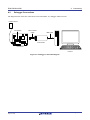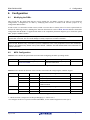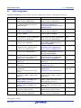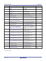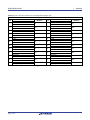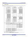
1
User`s Manual RX63N Group 32 32 Renesas Starter Kit+ User’s Manual For e2 studio RENESAS MCU RX Family / RX600 Series All information contained in these materials, including products and product specifications, represents information on the product at the time of publication and is subject to change by Renesas Electronics Corp. without notice. Please review the latest information published by Renesas Electronics Corp. through various means, including the Renesas Electronics Corp. website (http://www.renesas.com). Rev.1.00 Aug 2014 Disclaimer By using this Renesas Starter Kit (RSK+), the user accepts the following terms: The RSK+ is not guaranteed to be error free, and the entire risk as to the results and performance of the RSK+ is assumed by the User. The RSK+ is provided by Renesas on an “as is” basis without warranty of any kind whether express or implied, including but not limited to the implied warranties of satisfactory quality, fitness for a particular purpose, title and non-infringement of intellectual property rights with regard to the RSK+. Renesas expressly disclaims all such warranties. Renesas or its affiliates shall in no event be liable for any loss of profit, loss of data, loss of contract, loss of business, damage to reputation or goodwill, any economic loss, any reprogramming or recall costs (whether the foregoing losses are direct or indirect) nor shall Renesas or its affiliates be liable for any other direct or indirect special, incidental or consequential damages arising out of or in relation to the use of this RSK+, even if Renesas or its affiliates have been advised of the possibility of such damages. Precautions The following precautions should be observed when operating any RSK+ product: This Renesas Starter Kit is only intended for use in a laboratory environment under ambient temperature and humidity conditions. A safe separation distance should be used between this and any sensitive equipment. Its use outside the laboratory, classroom, study area or similar such area invalidates conformity with the protection requirements of the Electromagnetic Compatibility Directive and could lead to prosecution. The product generates, uses, and can radiate radio frequency energy and may cause harmful interference to radio communications. However, there is no guarantee that interference will not occur in a particular installation. If this equipment causes harmful interference to radio or television reception, which can be determined by turning the equipment off or on, you are encouraged to try to correct the interference by one or more of the following measures; • ensure attached cables do not lie across the equipment • reorient the receiving antenna • increase the distance between the equipment and the receiver • connect the equipment into an outlet on a circuit different from that which the receiver is connected • power down the equipment when not in use • consult the dealer or an experienced radio/TV technician for help NOTE: It is recommended that wherever possible shielded interface cables are used. The product is potentially susceptible to certain EMC phenomena. To mitigate against them it is recommended that the following measures be undertaken; • The user is advised that mobile phones should not be used within 10m of the product when in use. • The user is advised to take ESD precautions when handling the equipment. The Renesas Starter Kit does not represent an ideal reference design for an end product and does not fulfil the regulatory standards for an end product. How to Use This Manual 1. Purpose and Target Readers This manual is designed to provide the user with an understanding of the RSK+ hardware functionality, and electrical characteristics. It is intended for users designing sample code on the RSK+ platform, using the many different incorporated peripheral devices. The manual comprises of an overview of the capabilities of the RSK+ product, but does not intend to be a guide to embedded programming or hardware design. Further details regarding setting up the RSK+ and development environment can found in the tutorial manual. Particular attention should be paid to the precautionary notes when using the manual. These notes occur within the body of the text, at the end of each section, and in the Usage Notes section. The revision history summarizes the locations of revisions and additions. It does not list all revisions. Refer to the text of the manual for details. The following documents apply to the RSK+RX63N-256K. Make sure to refer to the latest versions of these documents. The newest versions of the documents listed may be obtained from the Renesas Electronics Web site. Document Type Description Document Title Document No. User’s Manual Describes the technical details of the RSK+ hardware. RSK+RX63N-256K User Manual R20UT3076EG Tutorial Manual Provides a guide to setting up RSK+ environment, running sample code and debugging programs. RSK+RX63N-256K Tutorial Manual R20UT3077EG Quick Start Guide Provides simple instructions to setup the RSK+ and run the first sample, on a single A4 sheet. RSK+RX63N-256K Quick Start Guide R20UT3078EG USB Function Manual Provides sample instructions to configure the RSK+ and Host PC for running the USB function sample code. RSK+RX63N USB Function Manual R20UT0442EG Schematics Full detail circuit schematics of the RSK+. RSK+RX63N-256K Schematics R20UT0437EG User’s Manual: Hardware Provides technical details of the RX63N microcontroller. RX63N Group, RX631 Group User's Manual: Hardware R01UH0041EJ 2. List of Abbreviations and Acronyms Abbreviation Full Form ADC Analog-to-Digital Converter bps CAN bits per second Controller-Area Network CPU CRC Central Processing Unit Cyclic Redundancy Check DIP DMA Dual In-line Package Direct Memory Access DMAC E1 Direct Memory Access Controller On-chip Debugger EEPROM EMC Electronically Erasable Programmable Read Only Memory Electromagnetic Compatibility ESD 2 IC Electrostatic Discharge Phillips™ Inter-Integrated Circuit Connection Bus IC IRQ Integrated Circuit Interrupt Request LCD LED Liquid Crystal Display Light Emitting Diode MAC MCU Media Access Control Micro-controller Unit MTU OTG Multifunction Timer Unit On The Go™ PC PCB Program Counter or Personal Computer Printed Circuit Board PLL PWM Phase Locked Loop Pulse Width Modulation RSK+ RSPI Renesas Starter Kit+ Renesas Serial Peripheral Interface SDRAM SFR Synchronous Dynamic Random Access Memory Special Function Register SPI SRAM Serial Peripheral Interface Static Random Access Memory TFT UART Thin Film Transistor Universal Asynchronous Receiver/Transmitter USB Universal Serial Bus All trademarks and registered trademarks are the property of their respective owners Table of Contents 1. Overview ............................................................................................................................................ 8 1.1 1.2 1.3 Purpose...................................................................................................................................................................... 8 Features ..................................................................................................................................................................... 8 Scope......................................................................................................................................................................... 8 2. Power Supply ..................................................................................................................................... 9 2.1 2.2 Requirements ............................................................................................................................................................ 9 Power-Up Behaviour................................................................................................................................................. 9 3. Board Layout ................................................................................................................................... 10 3.1 3.2 3.3 Component Layout.................................................................................................................................................. 10 Board Dimensions ....................................................................................................................................................11 Component Placement ............................................................................................................................................ 12 4. Connectivity ..................................................................................................................................... 14 4.1 4.2 Internal RSK+ Connections .................................................................................................................................... 14 Debugger Connections ............................................................................................................................................ 15 5. User Circuitry................................................................................................................................... 16 5.1 5.2 5.3 5.4 5.5 5.6 5.7 5.8 5.9 5.10 5.11 5.12 5.13 5.14 Reset Circuit............................................................................................................................................................ 16 Clock Circuit ........................................................................................................................................................... 16 Switches .................................................................................................................................................................. 16 LEDs ....................................................................................................................................................................... 17 Potentiometer .......................................................................................................................................................... 17 Debug LCD Module ............................................................................................................................................... 17 RS232 Serial Port.................................................................................................................................................... 18 Controller-Area Network (CAN) ............................................................................................................................ 18 Ethernet ................................................................................................................................................................... 19 Universal Serial Bus (USB) .................................................................................................................................... 20 Generic LCD Header .............................................................................................................................................. 21 External Bus ............................................................................................................................................................ 22 Renesas Serial Peripheral Interface (RSPI) ............................................................................................................. 22 I2C Bus (Inter-IC Bus) ............................................................................................................................................ 22 6. Configuration ................................................................................................................................... 23 6.1 6.2 6.3 6.4 6.5 6.6 6.7 6.8 6.9 6.10 6.11 6.12 6.13 Modifying the RSK+............................................................................................................................................... 23 MCU Configuration ................................................................................................................................................ 23 ADC Configuration ................................................................................................................................................. 24 RS232 Serial Port Configuration ............................................................................................................................ 25 CAN Configuration ................................................................................................................................................. 26 External Bus Configuration .................................................................................................................................... 27 USB Configuration ................................................................................................................................................. 29 Ethernet Configuration ............................................................................................................................................ 32 Multi-Function Timer Pulse Unit (MTU) Configuration ........................................................................................ 34 IRQ & General I/O Pin Configuration .................................................................................................................... 35 Power Supply Configuration ................................................................................................................................... 37 Clock Configuration................................................................................................................................................ 39 External Memory Configuration ............................................................................................................................. 39 7. Headers ............................................................................................................................................ 41 7.1 7.2 Application Headers ................................................................................................................................................ 41 Generic Headers ...................................................................................................................................................... 46 8. Code Development........................................................................................................................... 48 8.1 Overview ................................................................................................................................................................. 48 8.2 8.3 8.4 8.5 Compiler Restrictions ............................................................................................................................................. 48 Mode Support.......................................................................................................................................................... 48 Debugging Support ................................................................................................................................................. 48 Address Space ......................................................................................................................................................... 49 9. Additional Information..................................................................................................................... 50 RSK+RX63N-256K R20UT3076EG0100 Rev. 1.00 Aug 14, 2014 RENESAS STARTER KIT+ 1. Overview 1.1 Purpose This RSK+ is an evaluation tool for Renesas microcontrollers. This manual describes the technical details of the RSK+ hardware. The Quick Start Guide and Tutorial Manual provide details of the software installation and debugging environment. 1.2 Features This RSK+ provides an evaluation of the following features: • Renesas microcontroller programming • User code debugging • User circuitry such as switches, LEDs and a potentiometer • Sample application • Sample peripheral device initialisation code The RSK+ board contains all the circuitry required for microcontroller operation. 1.3 Scope This manual covers the RSK+RX63N-256K which is fitted a R5F563NFDDFC microcontroller. For the RSK+RX63N please http://www.renesas.com/rskrx63n. R20UT3076EG0100 Rev. 1.00 Aug 14, 2014 refer to User Manual R20UT2043EG, which can be found at Page 8 of 54 RSK+RX63N-256K 2. Power Supply 2. Power Supply 2.1 Requirements This RSK+ is supplied with an E1 debugger. The debugger is able to supply the RSK+ board with up to 200mA. In applications requiring more than 200mA or when the E1 debugger is not used, the RSK+ must be powered externally. All RSK and RSK+ boards have a centre positive supply connector using a 2.0mm barrel power jack. This RSK+ supports a wide range of voltage inputs, and requires specific configuration for different inputs. Details of the external power supply connections are shown in Table 2-1 below. Connector PWR1 Supply Voltages J8 Setting J9 Setting Regulated, 5V DC Shorted Shorted Unregulated, 7 to 15V DC Open Open Table 2-1: Main Power Supply Requirements The main power supply connected to PWR1 should supply a minimum of 5W to ensure full functionality. This RSK+ features an independent USB power supply, which allows a user to power the USB host/OTG modules from a second external power supply. Connections for the external USB power supply are detailed in Table 2-2 below. Connector Supply Voltages PWR2 (USB_3V3) Regulated, 3.3V DC PWR3 (USB_5V) Regulated, 5V DC Table 2-2: USB Power Supply Requirements The USB power supplies connected to PWR2 and PWR3 should both supply a minimum of 600mA to ensure full USB host functionality. Note: The OTG module is limited to supply a maximum of 200mA when operating as host. The RSK+ can also be powered directly from the USB VBUS, when a suitable host device is connected to the USB0 connector and the RSK+ is correctly configured (refer to §6). This will limit the current consumption of the RSK+ to 500mA (USB maximum), therefore full functionality cannot be achieved whilst being powered from the USB VBUS. This RSK+ also features a coin cell backup battery function which is used to power the real-time clock and subclock oscillator when the voltage drop at the VCC pin is detected. Connections for the backup battery power supply are detailed in Table 2-3 below. Connector PWR4 Supply Voltage 2.3V to 3.6V DC Table 2-3: Backup Battery Power Supply Requirements 2.2 Power-Up Behaviour When the RSK+ is purchased, the RSK+ board has the ‘Release’ or stand-alone code from the example tutorial code pre-programmed into the Renesas microcontroller. On powering up the board the user LEDs will start to flash. After 200 flashes or after pressing any switch, the LEDs will flash at a rate controlled by the potentiometer. R20UT3076EG0100 Rev. 1.00 Aug 14, 2014 Page 9 of 54 RSK+RX63N-256K 3. Board Layout 3. Board Layout 3.1 Component Layout Figure 3-1 below shows the top component layout of the board. Ethernet Status LEDs Application Board Interfaces USB1 (Function) USB0 (Host) USB0 (Function) Ethernet Connector JA5 JA6 RS232 Serial RX63N Application Board Interfaces Debug LCD Header CAN JA1 JA2 DC Power Jack 7 to 15V Input or 5V Input SW4 5V_PWR 3V3_PWR DIP Switch 32bit Data Bus Hrader TFT Generic TFT LCD Header JA3 Application Board Interfaces J22 Potentiometer Battery Holder User Switches E1 Header User LEDs Reset Switch Figure 3-1: Board Layout R20UT3076EG0100 Rev. 1.00 Aug 14, 2014 Page 10 of 54 RSK+RX63N-256K 3.2 3. Board Layout Board Dimensions 7.00mm Figure 3-2 below gives the board dimensions and connector positions. All the through-hole connectors are on a common 0.1 inch grid for easy interfacing. 7.00mm 3.2mm USB 150.00mm JA1 JA2 LCD 128.00mm JA5 JA6 Seria l RX63N 143.00mm 68.64mm Ether net 119.44mm USB 111.82mm USB 104.20mm 3.2mm 110.00mm 12.00mm 40.00mm 3.00mm CAN SW4 PWR TFT JA3 J22 Battery Holder E1 7.00mm 8.81mm 10.00mm 19.00mm 85.01mm 90.00mm 97.71mm 173.00mm 180.00mm Figure 3-2: Board Dimensions R20UT3076EG0100 Rev. 1.00 Aug 14, 2014 Page 11 of 54 RSK+RX63N-256K 3.3 3. Board Layout Component Placement Figure 3-3 below shows placement of individual components on the top-side PCB – bottom-side component placement can be seen in Figure 3-4. Component types and values can be looked up using the board schematics. R240 C72 R343 T20 R208 C86 R100 R107 R98 R367 R105 R365 R232 R231 R361 R328 C88 C87 C58 PWR 3 PWR 2 D9 R280 C85 C84 R276 /L3 T17 R273 R274 R275 R271 J3 T2 J15 R2 R58 R1 R71 C15 C19 C5 C6 R261 R262 R264 R128 R126 R23 R22 R19 R17 C27 C26 R18 R26 R21 R25 R27 C31 J16 L4 USB0_1 R68 C79 D10 R270 C83 T14 C76 R156 R155 J18 R139 U12 /L2 R256 R254 C77 R138 J4 C41 GND5 R141 U5 JA5 R373 R253 USB0_3 T13 R38 R36 R99 R96 R91 R89 R87 R85 R34 R43 R41 T4 R83 R356 R132 R135 R136 R133 J7 R134 R137 C81 R140 R374 T12 T3 RES C78 U13 R65 C29 R257 GND2 C80 R217 R218 X2 R129 R127 R125 R4 J1 X3 X1 T15 C30 T8 R16 C24 R15 T7 R24 R263 R259 R260 D8 C4 R93 JA1 R277 T16 R3 C1 C2 R20 RV1 R272 R76 C3 C28 C21 USB1 D11 J19 R258 R13 L5 C16 C17 J6 R117 R368 R369 PWR4 R88 R90 R92 C18 C20 C25 R116 T9 T6 T5 R86 C60 R55 R278 R279 T1 C14 C43 LED2 R237 U1 C13 C42 R81 R219 R250 R95 C82 J20 C8 C7 U6 R248 T11 C9 C12 TFT JA3 C62 C61 LED1 C22 R267 R266 R268 J2 C10 C57 U15 J21 R359 R82 J22 E20 R195 R190 R191 R193 C23 R265 R281 C11 R194 R14 J17 C36 C33 R192 LED3 R33 U2 C37 LED0 R77 R63 R78 R50 R51 R220 C39 C32 GND6 C106 R45 R47 R49 R57 R189 R187 R39 R185 R35 R37 R53 R226 R225 R224 R64 R67 R72 R223 R222 R221 U3 R238 C34 C59 R111 R109 R106 GND4 R121 R122 R285 R298 X5 X4 J5 JA6 C35 R327 R326 R324 R325 R329 L7 C95 C91 C93 U14 R212 L6 R119 C38 T18 C96 C97 C98 C92 L8 J13 R214 JA2 R120 T19 R206 J12 R213 R211 SPEED R306 R54 R70 R108 R75 R60 R74 R110 R69 R66 R186 R341 C99 C94 C89 R112 R184 R198 R203 R196 R338 R337 C67 R215 C100 C90 R62 R59 R200 R332 C104 C103 R340 R216 R115 R201 R202 R331 C101 C102 R151 R188 R152 E1 R199 R197 J10 R114 R334 R333 SW4 R113 R182 T21 R344 C105 R207 C69 DUPLEX C56 R150 R339 R342 C66 R209 R210 C55 U10 Product Label U7 D3 D4 SW3 L1 C49 C47 C70 C68 J11 R252 R251 R148 J9 R149 J8 D2 D5 C51 GND3 SW2 C48 C46 R204 R205 C75 LCD GND1 R245 U11 C73 R244 R147 SERIAL C71 R239 C45 C44 ETHERNET R243 J14 D1 C50 SW1 U8 T10 PWR1 POWER1(5V_PWR) POWER2 (3V3_PWR) RCAN Figure 3-3: Top-Side Component Placement R20UT3076EG0100 Rev. 1.00 Aug 14, 2014 Page 12 of 54 RSK+RX63N-256K 3. Board Layout R161 R160 C74 R247 R246 R242 R241 MAC Address C52 C53 R303 R321 R296 R302 R294 R313 R295 R287 R286 Serial Number R304 R322 R284 R168 R293 R167 R314 R166 R319 R330 R323 R159 R297 R335 R158 D6 R157 R336 R292 R309 C54 R308 R307 R305 R299 R283 R315 R372 R300 R289 R288 R320 R301 R318 R312 R317 R311 R316 R310 R180 R179 R291 R290 R349 R181 R183 R178 R355 R362 JA6 JA2 R353 R101 R102 R97 R233 R234 R347 R348 R358 R124 R123 R118 R236 R235 R351 J22 R354 R32 R176 R177 R172 R173 R175 R174 R146 R94 R371 R31 R230 R228 R229 R143 R360 R144 R370 R30 R28 R29 R366 JA3 TFT R364 R363 R227 R142 R145 R40 R162 R42 R163 R249 R7 R5 R6 R352 R44 R164 R46 R165 R170 USB0_1 R171 U9 U4 C64 R169 C65 D7 R269 R61 R73 R255 R56 R282 USB0_2 C40 R350 C63 R9 R10 R153 R154 R12 R48 R131 R130 R52 R84 R357 R346 R345 JA5 R11 JA1 Figure 3-4: Bottom-Side Component Placement R20UT3076EG0100 Rev. 1.00 Aug 14, 2014 Page 13 of 54 RSK+RX63N-256K 4. Connectivity 4. Connectivity 4.1 Internal RSK+ Connections The diagram below shows the RSK+ board components and their connectivity to the MCU. Power Jack Optional Jacks Backup Battery Boot Mode Switches 128Mbit SDRAM Application Board Headers VBATT Mode Pins VCC MCU Pin Headers 16Kbit I2C EEPROM Debug LCD 16Mbit SPI Serial Flash E1/E20 Debug Interface RX63N MCU Reset Switch Reset CAN IRQ RS-232 ADC I/O TFT Driver SW3 USB Function/Host Potentiometer SW1 SW2 User Switches Ethernet Power User LEDs O O R G R G Ethernet G G G LEDs Y Figure 4-1: Internal RSK+ Block Diagram R20UT3076EG0100 Rev. 1.00 Aug 14, 2014 Page 14 of 54 RSK+RX63N-256K 4.2 4. Connectivity Debugger Connections The diagram below shows the connections between the RSK+, E1 debugger and the host PC. External Power LCD Display User Interface Cable USB Cable E1 Emulator CPU Board Host PC Figure 4-2: Debugger Connection Diagram R20UT3076EG0100 Rev. 1.00 Aug 14, 2014 Page 15 of 54 RSK+RX63N-256K 5. User Circuitry 5. User Circuitry 5.1 Reset Circuit A reset control circuit is fitted to the RSK+ to generate the required reset signal, and is triggered from the RES switch. Refer to the RX63N Group, RX631 Group User’s Manual: Hardware for details regarding the reset signal timing requirements, and the RSK+RX63N board schematics for information regarding the reset circuitry in use on the RSK+. 5.2 Clock Circuit A clock circuit is fitted to the RSK+ to generate the required clock signal to drive the MCU, and associated peripherals. Refer to the RX63N Group, RX631 Group User’s Manual: Hardware for details regarding the clock signal requirements, and the RSK+RX63N board schematics for information regarding the clock circuitry in use on the RSK+. Details of the oscillators fitted to the RSK+ are listed in Table 5-1 below. Crystal X1 Function Default Placement Main MCU oscillator. Fitted Frequency 12MHz Device Package HC49/4U X2 Internal RSK+ Testing Only Unfitted n/a n/a X3 Real time Clock Fitted 32.768kHz Encapsulated, SMT X4 Ethernet Clock (MII) Fitted 25MHz HC49/4U X5 Ethernet Clock (RMII) Unfitted 50MHz Encapsulated, SMT Table 5-1: Oscillators 5.3 Switches There are four switches located on the RSK+ board. The function of each switch and its connection is shown in Table 5-2. For further information regarding switch connectivity, refer to the RSK+RX63N board schematics. Switch Function MCU Connection RES When pressed, the microcontroller is reset. RES#, Pin 21 SW1 Connects to an IRQ input for user controls. IRQ10, Pin 6 SW2 Connects to an IRQ input for user controls. IRQ8, Pin 8 SW3/ADTRG Connects to an IRQ input for user controls. The switch is also connected to an ATRG input, and is used to trigger AD conversions. IRQ15/ADTRG0#, Pin 176 Table 5-2: Switch Connections R20UT3076EG0100 Rev. 1.00 Aug 14, 2014 Page 16 of 54 RSK+RX63N-256K 5.4 5. User Circuitry LEDs There are ten LEDs on the RSK+ board. The function of each LED, its colour and connections are shown in Table 5-3. LED Colour Function MCU Connection 3V3_PWR Green Indicates the status of the 3.3V power rail. No connection 5V_PWR Green Indicates the status of the 5V power rail. No connection LED0 Green User operated LED. P03, Pin 4 LED1 Orange User operated LED. P05, Pin 2 LED2 Red User operated LED. P10, Pin 56 LED3 Red User operated LED. P11, Pin 55 SPEED Green Ethernet speed status LED. No connection DUPLEX Green Ethernet duplex status LED. P54, Pin 67* Built into Ethernet con. Green Ethernet link status LED. No connection Built into Ethernet con. Yellow Ethernet activity status LED. No connection Table 5-3: LED Connections * This connection is a not available in the default RSK+ configuration - refer to §6 for the required modifications. 5.5 Potentiometer A single-turn potentiometer is connected as a potential divider to analog input AN000, pin 173. The potentiometer can be used to create a voltage between AVCC0 and ground (by default, AVCC0 is connected to the MCU power supply UC_VCC). The potentiometer offers an easy method of supplying a variable analog input to the microcontroller. It does not necessarily reflect the accuracy of the controller’s ADC. Refer to the device hardware manual for further details. 5.6 Debug LCD Module A debug LCD module is supplied with the RSK+, and should be connected to the LCD header, LCD1. Care should be taken when installing the LCD module to ensure pins are not bent or damaged. The LCD module is vulnerable to electrostatic discharge (ESD); therefore appropriate ESD protection should be used. The debug LCD module uses a 4-bit interface to reduce pin allocation. No contrast control is provided, as this is set by a resistor supplied on the display module. Connection information for the debug LCD is provided in Table 5-4. Debug LCD Header Pin Circuit Net Name MCU Pin Pin Circuit Net Name MCU Pin 1 Ground - 2 Board_5V - 3 No Connection - 4 DLCDRS PJ5, Pin 11 5 R/W (Pulled to ground) - 6 DLCDE PF5, Pin 9 7 No Connection - 8 No Connection - 9 No Connection - 10 No Connection - 11 DLCDD4_XDRIVE P84, Pin 69 12 DLCDD5_YDRIVE P85, Pin 52 13 DLCDD6_BACKLIGHT P86, Pin 49 14 DLCDD7 P87, Pin 47 Table 5-4: LCD Header Connections R20UT3076EG0100 Rev. 1.00 Aug 14, 2014 Page 17 of 54 RSK+RX63N-256K 5.7 5. User Circuitry RS232 Serial Port Serial port SCI0 is connected to the standard RS232 header fitted to the RSK+. Alternatively, serial port SCI1 or SCI6 can be connected to the RS232 transceiver by making changes to the configurations to the jumpers and option links (refer to §6). Connections between the RS232 header and the microcontroller are listed in the Table 5-5. SCI Signal Function MCU Connection RS232 Connection TxD0 SCI0 Transmit Signal. P20, Pin P45 Pin 13 RxD0 SCI0 Receive Signal. P21, Pin P44 Pin 15 TxD1 SCI1 Transmit Signal. PF0, Pin 35 Pin 13* RxD1 SCI1 Receive Signal. PF2, Pin 31 Pin 15* TxD6 SCI6 Transmit Signal. P00, Pin 8 Pin 12* RxD6 SCI6 Receive Signal. P01, Pin 7 Pin 10* Table 5-5: Serial Port Connections * This connection is a not available in the default RSK+ configuration - refer to §6 for the required modifications. 5.8 Controller-Area Network (CAN) A CAN transceiver IC is fitted to the RSK+, and is connected to the CAN MCU peripheral. For further details regarding the CAN protocol and supported modes of operation, please refer to the RX63N Group, RX631 Group User’s Manual: Hardware. The connections for the CAN microcontroller signals are listed in Table 5-6 below. CAN Signal Function MCU Connection CTX1 CAN Data Transmission. P54, Pin 67 CRX1 CAN Data Reception. P55, Pin 66 CANEN CAN Transceiver Device Enable Control. PG1, Pin 144 CANERRn CAN Error and Power Status. P25, Pin 38 CANSTBn CAN Standby Mode Control. PG0, Pin 146 Table 5-6: CAN Connections R20UT3076EG0100 Rev. 1.00 Aug 14, 2014 Page 18 of 54 RSK+RX63N-256K 5.9 5. User Circuitry Ethernet When running any Ethernet software, a unique MAC address should be used. A unique Renesas allocated MAC address is attached to the RSK+RX63N PCB as a sticker, and should always be used with this device to ensure full compatibility when using other Renesas hardware on a common Ethernet connection. An Ethernet controller IC is fitted to the RSK+, and is connected to the Ethernet MCU peripheral. The RX63N MCU supports full duplex 10Mb/s and 100Mb/s transmission and reception. The Ethernet status LEDs (LED6 – 9) are detailed in §5.4. The connections for the Ethernet controller are listed in Table 5-7 below. Ethernet Signal Function MCU Connection ETMDIO Management data serial I/O P71, Pin 102 ETMDC Management serial clock P72, Pin 101 ETTXCLK Transmit clock PC4, Pin 82 ETTXEN Transmit enable. P80, Pin 81 ETTXER Transmit error. PC3, Pin 83 ETETXD0 Transmit data bit 0. P81, Pin 80 ETETXD1 Transmit data bit 1. P82, Pin 79 ETETXD2 Transmit data bit 2. PC5, Pin 78 ETETXD3 Transmit data bit 3. PC6, Pin 77 ETRXCLK Receive clock P76, Pin 85 ETRXDV Receive data valid. PC2, Pin 86 ETRXER Receive data error. P77, Pin 84 ETERXD0 Receive data bit 0. P75, Pin 87 ETERXD1 Receive data bit 1. P74, Pin 88 ETERXD2 Receive data bit 2. PC1, Pin 89 ETERXD3 Receive data bit 3. PC0, Pin 91 ETCOL Collision detect. PC7, Pin 76 ETLINKSTA Link status P54, Pin 67 ETCRS Carrier sense. P83, Pin 74 Table 5-7: Ethernet Connections R20UT3076EG0100 Rev. 1.00 Aug 14, 2014 Page 19 of 54 RSK+RX63N-256K 5.10 5. User Circuitry Universal Serial Bus (USB) This RSK+ device is fitted with a USB host socket (type A) and a function socket (type Mini B). USB module USB0 is connected to the host and function socket, and can operate as either a host or function device. Module USB1 is connected to a dedicated function port. The connections for the USB0 module are shown in Table 5-8 below. USB Signal Function MCU Connection USB0DP Positive differential data signal. USB0_DP, Pin 59 USB0DM Negative differential data signal. USB0_DM, Pin 58 USB0VBUS Cable monitor pin. P16, Pin 48 USB0EXICEN OTG low-power control signal. P21, Pin 44* USB0VBUSEN-H VBUS power supply enable (Host). P16, Pin 48 USB0VBUSEN-O VBUS power supply enable (OTG). P24, Pin 40* USB0OVRCURA Over-current detection signal A. P14, Pin 51 USB0OVRCURB Over-current detection signal B. P16, Pin 48* USB0ID USB ID pin. P20, Pin 45* USB0DPUPE-O Positive differential data pull-up control signal (OTG). P23, Pin 42* USB0DPUPE-F Positive differential data pull-up control signal (Function). P14, Pin 51 USB0DPRPD Differential data pull-down control signal. P25, Pin 38 USB0DRPD Differential data pull-down control signal. P22, Pin 43 Table 5-8: USB0 Module Connections Note: • • When evaluating OTG, ensure to replace the default USB connector (USB0_D) with a USB Micro-AB connector. Connectors such as the one manufactured by Hirose Electric with part number ZX62R-AB-5P, can be used. The connections for the USB1 module are shown in Table 5-9 below. USB Signal Function MCU Connection USB1DP Positive differential data signal. USB1_DP, Pin 64 USB1DM Negative differential data signal. USB1_DM, Pin 63 USB1VBUS VBUS power supply P17, Pin 46 USB1DPUPE Positive differential data pull-up control signal. P15, Pin 50 Table 5-9: USB1 Module Connections R20UT3076EG0100 Rev. 1.00 Aug 14, 2014 Page 20 of 54 RSK+RX63N-256K 5.11 5. User Circuitry Generic LCD Header This RSK+ device is fitted with a generic TFT LCD header, that allows connection to compatible Renesas LCD application boards. The pin connections of this header are listed in Table 5-10 below. Generic LCD Header (TFT) Pin Circuit Net Name MCU Pin Pin Circuit Net Name MCU Pin 1 5V - 2 5V - 3 3V3 - 4 3V3 - 5 Reserved - 6 Reserved - 7 B1 PD0, Pin 158 8 B2 PD1, Pin 156 9 B3 PD2, Pin 154 10 B4 PD3, Pin 150 11 B5 PD4, Pin 148 12 G0 PD5, Pin 147 13 G1 PD6, Pin 145 14 G2 PD7, Pin 143 15 G3 PE0, Pin 135 16 G4 PE1, Pin 134 17 G5 PE2, Pin 133 18 R1 PE3, Pin 132 19 R2 PE4, Pin 131 20 R3 PE5, Pin 130 21 R4 PE6, Pin 126 22 R5 PE7, Pin 125 23 EDACK P56, Pin 62 24 HSYNC P32, Pin 29 25 DOTCLK PJ3, Pin 13 26 LCDDEN P34, Pin 27 27 VSYNC P24, Pin 40 28 EDREQ P57, Pin 61 29 SSCK P27, Pin 36 30 SSI P30, Pin 33 31 SSO P26, Pin 37 32 SCS P50, Pin 72 33 RESET RES#, Pin 21 34 GND - 35 BACKLIGHT P86, Pin 49 36 SD_DOTCLK - 37 GND - 38 GND - 39 GND - 40 GND - 41 X_DRIVE P84, Pin 69 42 Y_DRIVE P85, Pin 52 43 X_INPUT1 P44, Pin 168 44 Y_INPUT1 P45, Pin 167 45 X_INPUT2 P46, Pin 166 46 Y_INPUT2 P47, Pin 165 47 Reserved - 48 Reserved - 49 Reserved - 50 Reserved - Table 5-10: Generic LCD Header Connections R20UT3076EG0100 Rev. 1.00 Aug 14, 2014 Page 21 of 54 RSK+RX63N-256K 5.12 5. User Circuitry External Bus The RX63N features an external data bus, which is connected to various devices on the RSK+ board. Details of the devices connected to the external data bus are listed in Table 5-11 below. Further details of the devices connected to the external bus can be found in the board schematics. Chip Select Device Name Device Description Address Space CS0 JA3 Application Header FF000000h to FFFFFFFFh (16Mbytes) SDCS U3 128MBit SDRAM 08000000h to 0FFFFFFFh (128Mbytes) JA3 Application Header 08000000h to 0FFFFFFFh (128Mbytes) CS1 to CS2 - Unused 06000000h to 07FFFFFFh (2 x 16Mbytes) CS3 JA3 Application Header 05000000h to 05FFFFFFh (16Mbytes) CS4 to CS7 - Unused 01000000h to 04FFFFFFh (4 x 16Mbytes) Table 5-11: External Bus Address Space 5.13 Renesas Serial Peripheral Interface (RSPI) The RX63N features three Renesas Serial Peripheral Interface modules (Renesas SPI or RSPI). Table 5-12 below details the connected devices, and their connections to the MCU. RSPI Channel Slave Select Device Name Device Description 1 SSLB0 U4 Serial Flash, 16Mbits 1 SSLB1 TFT Generic LCD Header Table 5-12: SPI Connections 5.14 I2C Bus (Inter-IC Bus) The RX63N features four I2C (Inter-IC Bus) interface modules. I2C module 0 is connected to a 16Kbit EEPROM (Electronically-Erasable Programmable Read Only Memory). Specific details of the EEPROM device and the connections can be found in the board schematics. This device is configured to respond to the address 0x3. The first bit of the device address can be configured by modifying option links – refer to §6 for further details. R20UT3076EG0100 Rev. 1.00 Aug 14, 2014 Page 22 of 54 RSK+RX63N-256K 6. Configuration 6. Configuration 6.1 Modifying the RSK+ This section lists the option links that are used to modify the way RSK+ operates in order to access different configurations. Configurations are made by modifying link resistors or headers with movable jumpers or by configuration DIP switches A link resistor is a 0Ω surface mount resistor, which is used to short or isolate parts of a circuit. Option links are listed in the following sections, detailing their function when fitted or removed. Bold, blue text indicates the default configuration that the RSK+ is supplied with. Refer to the component placement diagram (§3) to locate the option links, jumpers and DIP switches. When removing soldered components, always ensure that the RSK+ is not exposed to a soldering iron for intervals greater than 5 seconds. This is to avoid damage to nearby components mounted on the RSK+. When modifying a link resistor, always check the related option links to ensure there is no possible signal contention or short circuits. Because many of the MCU’s pins are multiplexed, some of the peripherals must be used exclusively. Refer to the RX63N Group, RX631 Group User’s Manual: Hardware and RSK+RX63N-256K board schematics for further information. 6.2 MCU Configuration Table 6-1 below details the option links associated with configuring the MCU operating modes. Reference R169 Link Fitted Configuration Link Removed Configuration Connects RESn (U1B, pin 21) to the reset switch RES. Disconnects RESn (U1B, pin 21) from the reset switch RES. Related Ref. U9 Table 6-1: MCU Option Links Table 6-2 below details the function of the switches associated with configuring the emulator support. Reference SW4 Pin 1 OFF Pin 2 OFF Operating Mode Single chip mode Related Ref. - ON OFF Boot mode (SCI) - OFF ON Single chip mode - ON ON User Boot Mode - USB Boot Mode Reference SW4 Pin 3 Pin 4 Operating Mode Related Ref. OFF x USB boot mode bus-powered* - ON x USB boot mode self-powered* - Table 6-2: MCU Setting DIP Switches x – Mode selection is irrespective of this pin changing (i.e. “Don’t care”). * To configure the device to power from the USB VBUS, see the USB configuration section (§6.7). R20UT3076EG0100 Rev. 1.00 Aug 14, 2014 Page 23 of 54 RSK+RX63N-256K 6. Configuration Table 6-3 below details the different configurations and functions of the MCU operating mode jumpers. Reference J6 Position One Pins 1 and 2 shorted. Connects EMLE (U1B, pin 10) to Board_VCC. Position Two Position Three Pins 2 and 3 shorted. Connects EMLE (U1B, pin 10) to GROUND. All pins open. EMLE is left to float – DO NOT SET. Related Ref. - Table 6-3: MCU Operating Mode Jumpers 6.3 ADC Configuration Table 6-4 & Table 6-5 below details the function of the option links associated with the Analog-to-Digital circuit. Reference Link Fitted Configuration Link Removed Configuration Related Ref. R5 Connects VREFH0 (U1A, pin 174) to UC_VCC. Disconnects VREFH0 (U1A, pin 174) from UC_VCC. R6* R6* Connects VREFH0 (U1A, pin 174) to CON_VREFH0 (JA1, pin 7). Disconnects VREFH0 (U1A, pin 174) from CON_VREFH0 (JA1, pin 7). R5 R7 Connects VREFL0 (U1A, pin 172) to GROUND. Disconnects VREFL0 (U1A, pin 172) from GROUND. - R9 Connects AVCC0 (U1A, pin 175) to UC_VCC. Disconnects AVCC0 (U1A, pin 175) from UC_VCC. R10* R10* Connects AVCC0 (U1A, pin 175) to CON_AVCC0 (JA1, pin 5). Disconnects AVCC0 (U1A, pin 175) from CON_AVCC0 (JA1, pin 5). R9 R11 Connects AVSS0 (U1A, pin 1) to GROUND. Disconnects AVSS0 (U1A, pin 1) from GROUND. R12* R12* Connects AVSS0 (U1A, pin 1) to CON_AVSS0 (JA1, pin 6). Disconnects AVSS0 (U1A, pin 1) from CON_AVSS0 (JA1, pin 6). R11 R13 Connects ADPOT (RV1) to Board_VCC. Disconnects ADPOT (RV1) from Board_VCC. R14* R14* Connects ADPOT (RV1) to CON_AVCC0 (JA1, pin 5). Disconnects ADPOT (RV1) from CON_AVCC0 (JA1, pin 5). R13 R15 Connects VREFH (U1A, pin 3) to UC_VCC. Disconnects VREFH (U1A, pin 3) from UC_VCC. - R16 Connects VREFL (U1A, pin 5) to GROUND. Disconnects VREFL (U1A, pin 5) from GROUND. ** R83* Connects AN000_ADPOT (U1C, pin 173) to AN000 (JA1, pin 9). Disconnects AN000_ADPOT (U1C, pin 173) from AN000 (JA1, pin 9). R84 R84 Connects AN000_ADPOT (U1C, pin 173) to ADPOT (RV1). Disconnects AN000_ADPOT (U1C, pin 173) from ADPOT (RV1). R83* R85* Connects AN004_XINPUT1 (U1C, pin 168) to AN004 (JA5, pin 1). Disconnects AN004_XINPUT1 (U1C, pin 168) from AN004 (JA5, pin 1). - Table 6-4: ADC Option Links (Continued Overleaf) * Do not fit the related reference link when the reference link is fitted. ** Do not remove. R20UT3076EG0100 Rev. 1.00 Aug 14, 2014 Page 24 of 54 RSK+RX63N-256K Reference 6. Configuration Link Fitted Configuration Link Removed Configuration Related Ref. R87* Connects AN005_YINPUT1 (U1C, pin 167) to AN005 (JA5, pin 2). Disconnects AN005_YINPUT1 (U1C, pin 167) from AN005 (JA5, pin 2). R88 R89* Connects AN006_XINPUT2 (U1C, pin 166) to AN006 (JA5, pin 3). Disconnects AN006_XINPUT2 (U1C, pin 166) from AN006 (JA5, pin 3). R90 R91* Connects AN007_YINPUT2 (U1C, pin 165) to AN007 (JA5, pin 4). Disconnects AN007_YINPUT2 (U1C, pin 165) from AN007 (JA5, pin 4). R92 Table 6-5: ADC Option Links (Continuation) * Do not fit the related reference link when the reference link is fitted. 6.4 RS232 Serial Port Configuration Table 6-6 below details the function of the option links associated with serial port configuration. Reference Link Fitted Configuration Link Removed Configuration Related Ref. R35* Connects IRQ8_TXD6 (U1B, pin 8) to TXD6 (JA6, pin 8). Disconnects IRQ8_TXD6 (U1B, pin 8) from TXD6 (JA6, pin 8) R34 R37* Connects IRQ9_RXD6 (U1B, pin 7) to RXD6 (JA6, pin 7). Disconnects IRQ9_RXD6 (U1B, pin 7) from RXD6 (JA6, pin 7). R36 R39 Connects IRQ10_SCK6 (U1B, pin 6) to SCK6 (JA6, pin 10). Disconnects IRQ10_SCK6 (U1B, pin 6) from SCK6 (JA6, pin 10). R38 R59 Connects TXD0_TRIGb_USB0ID (U1B, pin 45) to TXD0 (JA2, pin 6) Disconnects TXD0_TRIGb_USB0ID (U1B, pin 45) from TXD0 (JA2, pin 6) R60*, R61* R62 Connects RXD0_MTIOC1B_TRIGa_USB0EXICEN (U1B, pin 44) to RXD0 (JA2, pin 8) Disconnects RXD0_MTIOC1B_TRIGa_USB0EXICEN (U1B, pin 44) from RXD0 (JA2, pin 8) R63*, R64*, R65* R66 Connects SCK0_TMR0_USB0DRPD (U1B, pin 43) to SCK0 (JA2, pin 10) Disconnects SCK0_TMR0_USB0DRPD (U1B, pin 43) from SCK0 (JA2, pin 10) R67*, R68* R69 Connects CTS0RTS0_TMR1_USB0DPUPE-O (U1B, pin 42) to CTS0RTS0 (JA2, pin 12). Disconnects CTS0RTS0_TMR1_USB0DPUPE-O (U1B, pin 42) from CTS0RTS0 (JA2, pin 12). R70*, R71* R185 Connects TDO_TXD1 (U1B, pin 35) to TXD1 (JA6, pin 9) Disconnects TDO_TXD1 (U1B, pin 35) from TXD1 (JA6, pin 9) R184 R189 Connects TDI_RXD1 (U1B, pin 31) to RXD1 (JA2, pin 8) Disconnects TDI_RXD1 (U1B, pin 31) from RXD1 (JA2, pin 8) R188 R187* Connects TCK_SCK1 (U1B, pin 34) to SCK1 (JA2, pin 10) Disconnects TCK_SCK1 (U1B, pin 34) from SCK1 (JA2, pin 10) R186 R215 Connects TXD6 (JA6, pin 8) to T2IN (U10, pin 12). Disconnects TXD6 (JA6, pin 8) from T2IN (U10, pin 12). R34, R35* R216 Connects RXD6 (JA6, pin 7) to R2OUT (U10, pin 10). Disconnects RXD6 (JA6, pin 7) from R2OUT (U10, pin 10). R36, R37* Table 6-6: RS232 Serial Port Option Links * Not fitted by default. R20UT3076EG0100 Rev. 1.00 Aug 14, 2014 Page 25 of 54 RSK+RX63N-256K 6. Configuration Table 6-7 below details the different configurations and functions of the RS232 serial jumpers. Reference J12 Position One Position Two Position Three (Pin 1 and 2 Shorted) (Pin 2 and 3 Shorted) (All Pins Open) Connects TXD0 (U1B, pin 45) to T1IN (U10, pin 13) Connects TXD1 (U1B, pin 35) to T1IN (U10, pin 13) Related Ref. Disconnects both lines. R59, R60* R61*, R184 R185, R213** J13 Connects RXD0 (U1B, pin 44) to R1OUT (U10, pin 15) Connects RXD1 (U1B, pin 31) to R1OUT (U10, pin 15) Disconnects both lines. R62, R63*, R64*, R65*, R188, R189, R214** Table 6-7: RS232 Serial Port Jumpers * Ensure to only fit one option link relating to TXD0 and RXD0. ** When fitted, set the configuration to ‘Position One’. 6.5 CAN Configuration Table 6-8 below details the function of the option links associated with CAN configuration. Reference Link Fitted Configuration Link Removed Configuration Related Ref. R74 Connects CANERRn_MTIOC4C_USB0DPRPD (U1B, pin 38) to CANERRn (U11, pin 8). Disconnects CANERRn_MTIOC4C_USB0DPRPD (U1B, pin 38) from CANERRn (U11, pin 8). R75*, R76* R96 Connects CTX1_ALE_ETLINKSTA (U1C, pin 67) to CTX1 (JA5, pin 5). Disconnects CTX1_ALE_ETLINKSTA (U1C, pin 67) from CTX1 (JA5, pin 5). R97*, R98* R99 Connects CRX1_WAITn (U1C, pin 66) to CRX1 (JA5, pin 6). Disconnects CRX1_WAITn (U1C, pin 66) from CRX1 (JA5, pin 6). R100* R239 Connects CTX1 to TXD (U11, pin 1). Disconnects CTX1 from TXD (U11, pin 1). R96 R240 Connects CRX1 to RXD (U11, pin 4). Disconnects CRX1 from RXD (U11, pin 4). R99 R244 Connects WAKE (U11, pin 9) to GROUND. Disconnects WAKE (U11, pin 9) from GROUND. - R245 Connects VBAT (U11, pin 10) to Board_5V. Disconnects VBAT (U11, pin 10) from Board_5V. J14 * R371 Connects D24_CANSTBn (U1C, pin 146) to CANSTBn (U11, pin 14). Disconnects D24_CANSTBn (U1C, pin 146) from CANSTBn (U11, pin 14). - R372 Connects D25_CANEN (U1C, pin 144) to CANEN (U11, pin 6). Disconnects D25_CANEN (U1C, pin 144) from CANEN (U11, pin 6). - Table 6-8: CAN Option Links * Not fitted by default. R20UT3076EG0100 Rev. 1.00 Aug 14, 2014 Page 26 of 54 RSK+RX63N-256K 6. Configuration Table 6-9 below details the different configurations and functions of the CAN jumpers. Reference J14* Position One Position Two Position Three (Pin 1 and 2 Shorted) (Pin 2 and 3 Shorted) (All Pins Open) Connects VBAT (U11, pin 10) to Board_5V. Connects VBAT (U11, pin 10) to Unregulated_VCC. VBAT (U11, pin 10) is not connected to a power supply. Related Ref. R245 Table 6-9: CAN Jumpers * Not fitted by default. J14 is bypassed by R245, connecting VBAT to Board_5V. 6.6 External Bus Configuration Table 6-10 & Table 6-11 below details the function of option links related to configuring the MCU’s external bus. Reference Link Fitted Configuration Link Removed Configuration Related Ref. R93* Connects WR0n_WRn_SSLB1 (U1C, pin 72) to WR0n (JA3, pin 48). Disconnects WR0n_WRn_SSLB1 (U1C, pin 72) from WR0n (JA3, pin 48). R94, R95, R237 R94 Connects WR0n_WRn_SSLB1 (U1C, pin 72) to WRn (JA3, pin 26). Disconnects WR0n_WRn_SSLB1 (U1C, pin 72) from WRn (JA3, pin 26). R93*, R95, R227 R97* Connects CTX1_ALE_ETLINKSTA (U1C, pin 67) to ALE (JA3, pin 46). Disconnects CTX1_ALE_ETLINKSTA (U1C, pin 67) from ALE (JA3, pin 46). R96, R98*, R233 R100* Connects CRX1_WAITn (U1C, pin 66) to WAITn (JA3, pin 45). Disconnects CRX1_WAITn (U1C, pin 66) from WAITn (JA3, pin 45). R99, R232* R101 Connects SDCSn (U1C, pin 139) to BD_SDCSn (U3, pin 19). Disconnects SDCSn (U1C, pin 139) from BD_SDCSn (U3, pin 19) R102* R102* Connects SDCSn (U1C, pin 139) to CON_SDCSn (JA3, pin 28). Disconnects SDCSn (U1C, pin 139) from CON_SDCSn (JA3, pin 28). R101 R217* Connects RSPCKB (U1B, pin 36) to TFT_RSPCKB. Disconnects RSPCKB (U1B, pin 36) from TFT_RSPCKB. R28, R248 R218* Connects MOSIB (U1B, pin 37) to TFT_MOSIB. Disconnects MOSIB (U1B, pin 37) from TFT_MOSIB. R29, 250 R219* Connects MISOB (U1B, pin 33) to TFT_MISOB. Disconnects MISOB (U1B, pin 33) from TFT_MISOB. R30. R249 R227 Connects WRn (U1C, pin 72) to JA3_PIN26 (JA3, pin 26). Disconnects WRn (U1C, pin 72) from JA3_PIN26 (JA3, pin 26). R228* R228* Connects WEn (U1C, pin 136) to JA3_PIN26 (JA3, pin 26). Disconnects WEn (U1C, pin 136) from JA3_PIN26 (JA3, pin 26). R227 R229* Connects SDCLK (U1C, pin 128) to JA3_PIN44 (JA3, pin 44). Disconnects SDCLK (U1C, pin 128) from JA3_PIN44 (JA3, pin 44). R230* Table 6-10: External Bus Option Links (Continued Overleaf) * Not fitted by default. R20UT3076EG0100 Rev. 1.00 Aug 14, 2014 Page 27 of 54 RSK+RX63N-256K Reference 6. Configuration Link Fitted Configuration Link Removed Configuration Related Ref. R230* Connects BCLK (U1C, pin 68) to JA3_PIN44 (JA3, pin 44). Disconnects BCLK (U1C, pin 68) from JA3_PIN44 (JA3, pin 44). R229* R232* Connects WAITn (U1C, pin 66) to JA3_PIN45 (JA3, pin 45). Disconnects WAITn (U1C, pin 66) from JA3_PIN45 (JA3, pin 45). R100*, R231 R231 Connects CON_CS0n to JA3_PIN45 (JA3, pin 45). Disconnects CON_CS0n from JA3_PIN45 (JA3, pin 45). R232*, R360 R233 Connects ALE to JA3_PIN46 (JA3, pin 46). Disconnects ALE from JA3_PIN46 (JA3, pin 46). R234* R234* Connects CKE (U1C, pin 124) to JA3_PIN46 (JA3, pin 46). Disconnects CKE (U1C, pin 124) to JA3_PIN46 (JA3, pin 46). R233 R235 Connects WR1n to JA3_PIN47 (JA3, pin 47). Disconnects WR1n from JA3_PIN47 (JA3, pin 47). R236* R236* Connects DQM1 to JA3_PIN47 (JA3, pin 47). Disconnects DQM1 from JA3_PIN47 (JA3, pin 47). R235 R237 Connects WR0n to JA3_PIN48 (JA3, pin 48). Disconnects WR0n from JA3_PIN48 (JA3, pin 48). R238* R238 Connects DQM0 to JA3_PIN48 (JA3, pin 48). Disconnects DQM0 from JA3_PIN48 (JA3, pin 48). R237 R360 Connects CS0n (U1C, pin 141) to BD_CS0n (U6*, pin 32). Disconnects CS0n (U1C, pin 141) from BD_CS0n (U6*, pin 32). R361*, R370* R361* Connects CS0n (U1C, pin 141) to JA3_PIN45 (JA3, pin 45). Disconnects CS0n (U1C, pin 141) to JA3_PIN45 (JA3, pin 45). R231, R360 R366* Connects ETRXER_RMIIRXER_CS7n (U1C, pin 84) to CS7n (U6*, pin 32). Disconnects ETRXER_RMIIRXER_CS7n (U1C, pin 84) from CS7n (U6*, pin 32). R365, R370* R368* Connects ETCRS_RMIICRSDV_RYBYn (U1C, pin 74) to RYBYn (U6*, pin 17). Disconnects ETCRS_RMIICRSDV_RYBYn (U1C, pin 74) from RYBYn (U6*, pin 17). R367 R361* Table 6-11: External Bus Option Links (Continuation) * Not fitted by default. R20UT3076EG0100 Rev. 1.00 Aug 14, 2014 Page 28 of 54 RSK+RX63N-256K 6.7 6. Configuration USB Configuration Table 6-12 & Table 6-13 below details the function of option links related to configuring the USB ports. Reference Link Fitted Configuration Link Removed Configuration Related Ref. R55 Connects MTCLKB_USB1DPUPE (U1B, pin 50) to USB1DPUPE. Disconnects MTCLKB_USB1DPUPE (U1B, pin 50) from USB1DPUPE. R54* R56* Connects USB0VBUS_USB0VBUSENH_USB0OVRCURB (U1B, pin 48) to USB0OVRCURB. Disconnects USB0VBUS_USB0VBUSENH_USB0OVRCURB (U1B, pin 48) from USB0OVRCURB. J4 R58 Connects MTIOC3A_USB1VBUS (U1B, pin 46) to USB1VBUS. Disconnects MTIOC3A_USB1VBUS (U1B, pin 46) from USB1VBUS. R57* R61* Connects TXD0_TRIGb_USB0ID (U1B, pin 45) to USB0ID. Disconnects TXD0_TRIGb_USB0ID (U1B, pin 45) from USB0ID. R59, R60* R65* Connects RXD0_MTIOC1B_TRIGa_USB0EXICEN (U1B, pin 44) to USB0EXICEN. Disconnects RXD0_MTIOC1B_TRIGa_USB0EXICEN (U1B, pin 44) from USB0EXICEN. R62, R63*, R64* R68* Connects SCK0_TMR0_USB0DRPD (U1B, pin 43) to USB0DRPD. Disconnects SCK0_TMR0_USB0DRPD (U1B, pin 43) from USB0DRPD. R66, R67* R71* Connects CTS0RTS0_TMR1_USB0DPUPE-O (U1B, pin 42) to USB0DPUPE-O. Disconnects CTS0RTS0_TMR1_USB0DPUPE-O (U1B, pin 42) from USB0DPUPE-O. R69, R70* R73* Connects MTIOC4A_USB0VBUSEN-O (U1B, pin 40) to USB0VBUSEN-O. Disconnects MTIOC4A_USB0VBUSEN-O (U1B, pin 40) from USB0VBUSEN-O. R72 R76* Connects CANERRn_MTIOC4C_USB0DPRPD (U1B, pin 38) to USB0DPRPD. Disconnects CANERRn_MTIOC4C_USB0DPRPD (U1B, pin 38) from USB0DPRPD. R74, R75* R254 Connects USB0OVRCURA to FLG (U12, pin 2). Disconnects USB0OVRCURA from FLG (U12, pin 2). R255*, R53* J3 R255* Connects USB0OVRCURA to STATUS1 (U13, pin 5). Disconnects USB0OVRCURA from STATUS1 (U13, pin 5). R254 R258* Connects SHDN (U13, pin 11) to USB0EXICEN. Disconnects SHDN (U13, pin 11) from USB0EXICEN. R65*, R64*, R63*, R62 Shuts down U13 and reduces supply current. Enables the OTG normal operation. R265 Connects USB0VBUS to VBUS0 (USB Connectors: USB0_1, USB0_2 and USB0_3). Disconnects USB0VBUS from VBUS0 (USB Connectors: USB0_1, USB0_2 and USB0_3). J17*, J18 R270 Connects VBUS (USB Connectors: USB0_1, USB0_2 and USB0_3) to USB0_VBUSEL (J18, pin 2). Disconnects VBUS (USB Connectors: USB0_1, USB0_2 and USB0_3) from USB0_VBUSEL (J18, pin 2). L2* R271 Connects FRAME (USB Connectors: USB0_1, USB0_2 and USB0_3) to GROUND. Disconnects FRAME (USB Connectors: USB0_1, USB0_2 and USB0_3) from GROUND. - R272 Connects USB1VBUS to VBUS (USB Connector: USB1 Function). Disconnects USB1VBUS from VBUS (USB Connector: USB1 Function). J19* R276 Connects VBUS (USB Connector: USB1 Function) to USB1VBUS. Disconnects VBUS (USB Connector: USB1 Function) from USB1VBUS. L3*, R272 J15 Table 6-12: USB Option Links (Continued Overleaf) * Not fitted by default. R20UT3076EG0100 Rev. 1.00 Aug 14, 2014 Page 29 of 54 RSK+RX63N-256K Reference 6. Configuration Link Fitted Configuration R280 Link Removed Configuration Connects FRAME (USB Connectors: USB_1 Function) to GROUND. Related Ref. Disconnects FRAME (USB Connectors: USB_1 Function) from GROUND. - R281* Connects VBUS0 to VBUS Disconnects VBUS0 from VBUS. J20* R373 Connects USB0DP (U1B, pin 59) to D+ (USB Connectors: USB0_2 and USB0_3). Disconnects USB0DP (U1B, pin 59) from D+ (USB Connectors: USB0_2 and USB0_3). - R374 Connects USB0DM (U1B, pin 58) to D(USB Connectors: USB0_2 and USB0_3). Disconnects USB0DM (U1B, pin 58) from D- (USB Connectors: USB0_2 and USB0_3). - Table 6-13: USB Option Links (Continuation) * Not fitted by default. Table 6-14 below details the different configurations for the USB0DPUPE-F and USB0OVRCURA USB jumpers. Reference J3 J4 Position One Position Two Position Three (Pin 1 and 2 Shorted) (Pin 2 and 3 Shorted) (All Pins Open) Connects MTCLKA_USB0DPUPEF_USB0OVRCURA (U1B, pin 51) to USB0DPUPE-F. Connects MTCLKA_USB0DPUPEF_USB0OVRCURA (U1B, pin 51) to USB0OVRCURA. Unless R53 is fitted. Connects USB0VBUS_USB0VBUSENH_USB0OVRCURB (U1B, pin 48) to USB0VBUS. Connects USB0VBUS_USB0VBUSENH_USB0OVRCURB (U1B, pin 48) to USB0VBUSEN-H Unless R56 is fitted. Related Ref. Do not set. R53* Do not set. R56* Table 6-14: USB Jumpers USB0DPUPE-F / USB0OVRCURA Configuration * Not fitted by default. Table 6-15 below details the different configurations and functions for the USB0OVRCURA Selection. Reference R254 Link Configuration R255 Function Fitted Removed Host mode Removed Fitted OTG mode Related Ref. R53*, J3 Table 6-15: USB Mode USB0OVRCURA Configuration * Not fitted by default. Table 6-16 below details the different configurations and functions of the USB jumpers. Reference J15/J16* Position One Position Two (Pin 1 and 2 Shorted) (All Pins Open) Host mode Function and OTG mode Related Ref. - Table 6-16: USB Jumpers (USB0DPRPD, DRPD Pull-down Configuration) * Ensure J15 and J16 are set to the same position. R20UT3076EG0100 Rev. 1.00 Aug 14, 2014 Page 30 of 54 RSK+RX63N-256K 6. Configuration Table 6-17 below details the different configurations and functions of the USB jumpers. Reference Position J17* J20* Pin 1 and 2 shorted Function Pin 1 and 2 shorted Bus-powered (via R281) Pin 2 and 3 shorted All open Self-powered (via R265) Table 6-17: USB Jumpers (VBUS0 Self-powered/Bus-powered Configuration) * Not fitted by default. Ensure J17 and J20 have the same configuration. Table 6-18 below details the different configurations and functions of the USB jumpers. Reference J18 Position One Position Two Position Three (Pin 1 and 2 Shorted) (Pin 2 and 3 Shorted) (All Pins Open) Related Ref. Host mode. Function mode. OTG mode. (Ensure R269 is removed) (Ensure R269 is removed) (Ensure R269 is fitted) R269* Table 6-18: USB Jumpers (VBUS0 Host/Function/OTG Select) * Not fitted by default. Table 6-19 below details the different configurations and functions of the USB jumpers. Reference Position J19* Pin 1 and 2 shorted Pin 2 and 3 shorted (via R272) J20* Function Pin 2 and 3 shorted Bus-powered All open Self-powered Table 6-19: USB Jumpers (VBUS1 Self-powered/Bus-powered Configuration) * Not fitted by default. Note: The RSK+RX63N board is configured for Function mode USB operations. Table 6-20 below lists the required changes to configure the board for USB Host mode. Reference Position J3 Pin 2 and 3 shorted J4 Pin 2 and 3 shorted J15 Pin 1 and 2 shorted J16 Pin 1 and 2 shorted J18 Pin 1 and 2 shorted Table 6-20: USB0 Jumpers (Host Mode Configuration) R20UT3076EG0100 Rev. 1.00 Aug 14, 2014 Page 31 of 54 RSK+RX63N-256K 6.8 6. Configuration Ethernet Configuration Table 6-21 & Table 6-22 below details the function of option links related to configuring the MCU’s Ethernet peripheral. Reference Link Fitted Configuration Link Removed Configuration Related Ref. R98* Connects CTX1_ALE_ETLINKSTA to ETLINKSTA (U14, pin 10). Disconnects CTX1_ALE_ETLINKSTA from ETLINKSTA (U14, pin 10). R96, R97* R105 Connects ETRXDV_MTIOC4B to ETRXDV (U14, pin 19). Disconnects ETRXDV_MTIOC4B from ETRXDV (U14, pin 19) R106*, R299 R107 Connects ETTXER_MTIOC4D to ETTXER (U14, pin 1). Disconnects ETTXER_MTIOC4D from ETTXER (U14, pin 1) R108*, R295, R307*, R308* R109 Connects ETTXCLK_MTIOC3D to ETTXCLK (U14, pin 22). Disconnects ETTXCLK_MTIOC3D from ETTXCLK (U14, pin 22) R110*, R294 R111 Connects ETETXD2_MTIOC3B to ETETXD2 (U14, pin 26). Disconnects ETETXD2_MTIOC3B from ETETXD2 (U14, pin 26) R112*, R296, R322* R294 Connects ETTXCLK to U14 (pin 22) via U15 (pin 15). Disconnects ETTXCLK from U14 (pin 22). R109, R110* R295 Connects ETTXER to U14 (pin 1) via U15 (pin 14) and (R107). Disconnects ETTXER from U14 (pin 1). R107, R307* R296 Connects ETETXD2 to U14 (pin 26) via U15 (pin 16) and (R111). Disconnects ETETXD2 from U14 (pin 26). R111, R322* R297 Connects ETETXD3 to U14 (pin 27) via U15 (pin 17). Disconnects ETETXD3 from U14 (pin 27). R323* R298 Connects ETRXCLK_REF50CK (U1C, pin 85) to U14 (pin 20). Disconnects ETRXCLK_REF50CK (U1C, pin 85) from U14 (pin 20). - R299 Connects ETRXDV to U14 (pin 19) via U15 (pin 13). Disconnects ETRXDV from U14 (pin 19). R105 R300 Connects ETERXD2 to U14 (pin 16) via U15 (pin 12). Disconnects ETERXD2 from U14 (pin 16). R318* R301 Connects ETERXD3 to U14 (pin 15) via U15 (pin 11). Disconnects ETERXD3 from U14 (pin 15). R320 R302 Connects ETCOL to U14 (pin 36) via U15 (pin 18). Disconnects ETCOL from U14 (pin 36). R303* R303* Connects ETCRS_RMIICRSDV to U14 (pin 36). Disconnects ETCRS_RMIICRSDV from U14 (pin 36). R302, R304 R304 Connects ETCRS_RMIICRSDV to U14 (pin 3). Disconnects ETCRS_RMIICRSDV from U14 (pin 3). R319* R320 Connects ETERXD3 to GROUND, via R315. Disconnects ETERXD3 from GROUND. R315, R301 R322* Connects ETETXD2 to GROUND. Disconnects ETETXD2 from GROUND. R296 R323* Connects ETETXD3 to GROUND. Disconnects ETETXD3 from GROUND. R297 R324 Connects XTAL1 (U14, pin 14) to X4 (pin 1). Disconnects XTAL1 (U14, pin 14) from X4 (pin 1). R326 R308* Table 6-21: Ethernet Option Links (Continued Overleaf) * Not fitted by default. R20UT3076EG0100 Rev. 1.00 Aug 14, 2014 Page 32 of 54 RSK+RX63N-256K Reference 6. Configuration Link Fitted Configuration Link Removed Configuration Related Ref. R325 Connects XTAL2 (U14, pin 13) to X4 (pin 2). Disconnects XTAL2 (U14, pin 13) from X4 (pin 2). - R326* Connects XTAL1 (U14, pin 14) to X5 (pin 3). Disconnects XTAL1 (U14, pin 14) from X5 (pin 3). R327*, R324 R327* Connects X5 (pin 3) to ETRXCLK_REF50CK (U1C, pin 85) and U14 (pin 20). Disconnects X5 (pin 3) from ETRXCLK_REF50CK (U1C, pin 85) and U14 (pin 20). R326, R298 R328 Connects X5 (pin 1) to GROUND. Disconnects X5 (pin 1) from GROUND. - R339* Connects U14 (pin 9) to GROUND. Disconnects U14 (pin 9) from GROUND. - R340* Connects U14 (pin 12) to GROUND Disconnects U14 (pin 12) from GROUND - R341* Connects U14 (pin 11) to GROUND. Disconnects U14 (pin 11) from GROUND. - R342* Connects U14 (pin 10) to GROUND Disconnects U14 (pin 10) from GROUND - R344 Connects ETHERNET port (pin 10) to GROUND. Disconnects ETHERNET port (pin 10) from GROUND. R303*, R304, R368* R365 Connects ETRXER_RMIIRXER_CS7n (U1C, pin 84) to ETRXER_RMIIRXER (U14, pin 21). Disconnects ETRXER_RMIIRXER_CS7n (U1C, pin 84) from ETRXER_RMIIRXER (U14, pin 21). R366* R367 Connects ETCRS_RMIICRSDV_RYBYn (U1C, pin 74) to ETCRS_RMIICRSDV (U14, pin 3 or pin 36). Disconnects ETCRS_RMIICRSDV_RYBYn (U1C, pin 74) from ETCRS_RMIICRSDV (U14, pin 3 and pin 36). R303*, R304, R368* Table 6-22: Ethernet Option Links (Continuation) * Not fitted by default. R20UT3076EG0100 Rev. 1.00 Aug 14, 2014 Page 33 of 54 RSK+RX63N-256K 6.9 6. Configuration Multi-Function Timer Pulse Unit (MTU) Configuration Table 6-23 & Table 6-24 details the function of option links related to configuring the MCU’s MTU pins. Reference Link Fitted Configuration Link Removed Configuration R45* Connects LED2_MTIC5W (U1B, pin 56) to MTIC5W (JA6, pin 16). Disconnects LED2_MTIC5W (U1B, pin 56) from MTIC5W (JA6, pin 16). R44 R47* Connects LED3_MTIC5V (U1B, pin 55) to MTIC5V (JA6, pin 15). Disconnects LED3_MTIC5V (U1B, pin 55) from MTIC5V (JA6, pin 15). R46 R49* Connects MTIC5U_SCL0 (U1B, pin 54) to MTIC5U (JA6, pin 14). Disconnects MTIC5U_SCL0 (U1B, pin 54) from MTIC5U (JA6, pin 14). R48 R50* Connects MTIOC0B_IRQ3_SDA0 (U1B, pin 53) to MTIOC0B (JA2, pin 9). Disconnects MTIOC0B_IRQ3_SDA0 (U1B, pin 53) from MTIOC0B (JA2, pin 9). R51*, R52, R223* R53* Connects MTCLKA_USB0DPUPEF_USB0OVRCURA (U1B, pin 51) to MTCLKA (JA2, pin 25). Disconnects MTCLKA_USB0DPUPEF_USB0OVRCURA (U1B, pin 51) from MTCLKA (JA2, pin 25). J3 R54* Connects MTCLKB_USB1DPUPE (U1B, pin 50) to MTCLKB (JA2, pin 26). Disconnects MTCLKB_USB1DPUPE (U1B, pin 50) from MTCLKB (JA2, pin 26). R55 R57* Connects MTIOC3A_USB1VBUS (U1B, pin 46) to MTIOC3A (JA6, pin 13). Disconnects MTIOC3A_USB1VBUS (U1B, pin 46) from MTIOC3A (JA6, pin 13). R58 R60* Connects TXD0_TRIGb_USB0ID (U1B, pin 45) to TRIGb (JA2, pin 22). Disconnects TXD0_TRIGb_USB0ID (U1B, pin 45) from TRIGb (JA2, pin 22). R59, R61* R63* Connects RXD0_MTIOC1B_TRIGa_USB0EXICEN (U1B, pin 44) to MTIOC1B (JA2, pin 23). Disconnects RXD0_MTIOC1B_TRIGa_USB0EXICEN (U1B, pin 44) from MTIOC1B (JA2, pin 23). R62, R64*, R65*, R224 R255*,R226* R64* Connects RXD0_MTIOC1B_TRIGa_USB0EXICEN (U1B, pin 44) to TRIGa (JA2, pin 21). Disconnects RXD0_MTIOC1B_TRIGa_USB0EXICEN (U1B, pin 44) from TRIGa (JA2, pin 21). R62, R63*, R65* R67* Connects SCK0_TMR0_USB0DRPD (U1B, pin 43) to TMR0 (JA2, pin 19). Disconnects SCK0_TMR0_USB0DRPD (U1B, pin 43) to TMR0 (JA2, pin 19). R66, R68* R70* Connects CTS0RTS0_TMR1_USB0DPUPE-O (U1B, pin 42) to TMR1 (JA2, pin 20). Disconnects CTS0RTS0_TMR1_USB0DPUPE-O (U1B, pin 42) to TMR1 (JA2, pin 20). R69, R71* R72 Connects MTIOC4A_USB0VBUSEN-O (U1B, pin 40) to MTIOC4A (JA2, pin 15). Disconnects MTIOC4A_USB0VBUSENO (U1B, pin 40) from MTIOC4A (JA2, pin 15). R73* R75* Connects CANERRn_MTIOC4C_USB0DPRPD (U1B, pin 38) to MTIOC4C (JA2, pin 16). Disconnects CANERRn_MTIOC4C_USB0DPRPD (U1B, pin 38) from MTIOC4C (JA2, pin 16). R74, R76* R77 Connects MTIOC0C_IRQ2 (U1B, pin 29) to MTIOC0C (JA2, pin 23). Disconnects MTIOC0C_IRQ2 (U1B, pin 29) from MTIOC0C (JA2, pin 23). R224, R225* Connects MTIOC0A_IRQ4 (U1B, pin 27) to MTIOC0A (JA2, pin 7). Disconnects MTIOC0A_IRQ4 (U1B, pin 27) from MTIOC0A (JA2, pin 7). R82*, R220* R81 Related Ref. R226*, R78 R221 Table 6-23: MTU Option Links (Continued Overleaf) * Not fitted by default. R20UT3076EG0100 Rev. 1.00 Aug 14, 2014 Page 34 of 54 RSK+RX63N-256K 6. Configuration Reference Link Fitted Configuration Link Removed Configuration Related Ref. R106* Connects ETRXDV_MTIOC4B (U1C, pin 86) to MTIOC4B (JA2, pin 17) via U15. Disconnects ETRXDV_MTIOC4B (U1C, pin 86) from MTIOC4B (JA2, pin 17). R105 R108* Connects ETTXER_MTIOC4D (U1C, pin 83) to MTIOC4D (JA2, pin 18) via U15. Disconnects ETTXER_MTIOC4D (U1C, pin 83) from MTIOC4D (JA2, pin 18). R107 R110* Connects ETTXCLK_MTIOC3D (U1C, pin 82) to MTIOC3D (JA2, pin 14) via U15. Disconnects ETTXCLK_MTIOC3D (U1C, pin 82) from MTIOC3D (JA2, pin 14). R109 R112* Connects ETETXD2_MTIOC3B (U1C, pin 78) to MTIOC3B (JA2, pin 13) via U15. Disconnects ETETXD2_MTIOC3B (U1C, pin 78) from MTIOC3B (JA2, pin 13). R111 R221 Connects MTIOC0A (U1B, pin 27) to JA2_PIN7 (JA2, pin 7). Disconnects MTIOC0A (U1B, pin 27) from JA2_PIN7 (JA2, pin 7). R81, R220* R223* Connects MTIOC0B (U1B, pin 53) to JA2_PIN9 (JA2, pin 9). Disconnects MTIOC0B (U1B, pin 53) from JA2_PIN9 (JA2, pin 9). R50, R222 R225* Connects MTIOC1B (U1B, pin 44) to JA2_PIN23 (JA2, pin 23). Disconnects MTIOC1B (U1B, pin 44) from JA2_PIN23 (JA2, pin 23). R63, R224, R226* R226* Connects MTIOC0C (U1B, pin 29) to JA2_PIN23 (JA2, pin 23). Disconnects MTIOC0C (U1B, pin 29) from JA2_PIN23 (JA2, pin 23). R77, R224, R225* Table 6-24: MTU Option Links (Continuation) * Not fitted by default. 6.10 IRQ & General I/O Pin Configuration Table 6-25 & Table 6-26 below details the function of the option links associated with IRQ and general I/O pin configuration. Reference Link Fitted Configuration Link Removed Configuration Related Ref. R28 Connects RSPCKB to U1B (pin 36) Disconnects RSPCKB from U1B (pin 36) - R29 Connects MOSIB to U1B (pin 37) Disconnects MOSIB from U1B (pin 37) - R30 Connects MISOB to U1B (pin 33) Disconnects MISOB from U1B (pin 33) - R31 Connects BCLK to U1C (pin 68) Disconnects BCLK from U1C (pin 68) - R32 Connects SDCLK to U1C (pin 128) Disconnects SDCLK from U1C (pin 128) - R34 Connects IRQ8_TXD6 (U1B, pin 8) to IRQ8 (JA1, pin 23). Disconnects IRQ8_TXD6 (U1B, pin 8) from IRQ8 (JA1, pin 23). R35*, R167 R36 Connects IRQ9_RXD6 (U1B, pin 7) to IRQ9 (JA5, pin 9). Disconnects IRQ9_RXD6 (U1B, pin 7) from IRQ9 (JA5, pin 9). R37* R38 Connects IRQ10_SCK6 (U1B, pin 6) to IRQ10 (JA5, pin 10). Disconnects IRQ10_SCK6 (U1B, pin 6) from IRQ10 (JA5, pin 10). R39*, R166 R307* Table 6-25: IRQ & General I/O Option Links (Continued Overleaf) * Not fitted by default. R20UT3076EG0100 Rev. 1.00 Aug 14, 2014 Page 35 of 54 RSK+RX63N-256K Reference 6. Configuration Link Fitted Configuration Link Removed Configuration Related Ref. R40 Connects LED0_DA0 (U1B, pin 4) to LED0 Disconnects LED0_DA0 (U1B, pin 4) from LED0 R41* R42 Connects LED1_DA1 (U1B, pin 2) to LED1 Disconnects LED1_DA1 (U1B, pin 2) from LED1 R43* R44 Connects LED2_MTIC5W (U1B, pin 56) to LED2 Disconnects LED2_MTIC5W (U1B, pin 56) from LED2 R45* R46 Connects LED3_MTIC5V (U1B, pin 55) to LED3 Disconnects LED3_MTIC5V (U1B, pin 55) from LED3 R47* R48 Connects MTIC5U_SCL0 (U1B, pin 54) to SCL0 (U5, pin 6) Disconnects MTIC5U_SCL0 (U1B, pin 54) from SCL0 (U5, pin 6) R136, R49* R51* Connects MTIOC0B_IRQ3_SDA0 (U1B, pin 53) to IRQ3 (JA2, pin 9). Disconnects MTIOC0B_IRQ3_SDA0 (U1B, pin 53) from IRQ3 (JA2, pin 9). R50*, R52, R222 R52 Connects MTIOC0B_IRQ3_SDA0 (U1B, pin 53) to SDA0 (U5, pin 5) Disconnects MTIOC0B_IRQ3_SDA0 (U1B, pin 53) from SDA0 (U5, pin 5) R50*, R51 R135 R78* Connects MTIOC0C_IRQ2 (U1B, pin 29) to IRQ2 (JA2, pin 23). Disconnects MTIOC0C_IRQ2 (U1B, pin 29) from IRQ2 (JA2, pin 23). R77 R82* Connects MTIOC0A_IRQ4 (U1B, pin 27) to IRQ4 (JA2, pin 7). Disconnects MTIOC0A_IRQ4 (U1B, pin 27) from IRQ4 (JA2, pin 7). R81, R220* R69 Connects CTS0RTS0_TMR1_USB0DPUPE-O (U1B, pin 42) to CTS0RTS0 (JA2, pin 12) Disconnects CTS0RTS0_TMR1_USB0DPUPE-O (U1B, pin 42) from CTS0RTS0 (JA2, pin 12) R70*, R71* R86 Connects AN004_XINPUT1 (U1C, pin 168) to XINPUT1 (TFT connector, pin 43) Disconnects AN004_XINPUT1 (U1C, pin 168) from XINPUT1 (TFT connector, pin 43) R85* R88 Connects AN005_YINPUT1 (U1C, pin 167) to YINPUT1 (TFT connector, pin 44) Disconnects AN005_YINPUT1 (U1C, pin 167) from YINPUT1 (TFT connector, pin 44) R87* R90 Connects AN006_XINPUT2 (U1C, pin 166) to XINPUT2 (TFT connector, pin 45) Disconnects AN006_XINPUT2 (U1C, pin 166) from XINPUT2 (TFT connector, pin 45) R89* R92 Connects AN007_YINPUT2 (U1C, pin 165) to YINPUT2 (TFT connector, pin 46) Disconnects AN007_YINPUT2 (U1C, pin 165) from YINPUT2 (TFT connector, pin 46) R91* R95 Connects WR0n_WRn_SSLB1 (U1C, pin 72) to SSLB1 (TFT connector, pin 32) Disconnects WR0n_WRn_SSLB1 (U1C, pin 72) from SSLB1 (TFT connector, pin 32) R94, R93* R220* Connects IRQ4 (U1B, pin 27) to JA2_PIN7 (JA2, pin 7). Disconnects IRQ4 (U1B, pin 27) from JA2_PIN7 (JA2, pin 7). R82*, R221 R222 Connects IRQ3 (U1B, pin 54) to JA2_PIN9 (JA2, pin9). Disconnects IRQ3 (U1B, pin 54) from JA2_PIN9 (JA2, pin 9). R51*, R223* R224 Connects IRQ2 (U1B, pin 29) to JA2_PIN23 (JA2, pin 23). Disconnects IRQ2 (U1B, pin 29) from JA2_PIN23 (JA2, Pin23) R78*, R225*, R226* Table 6-26: IRQ & General I/O Option Links (Continuation) * Not fitted by default. R20UT3076EG0100 Rev. 1.00 Aug 14, 2014 Page 36 of 54 RSK+RX63N-256K 6. Configuration Table 6-27 below details the function of the jumpers associated with IRQ and general I/O pin configuration. Reference J5 Position One Position Two Pins 1 and 2 shorted. Position Three Pins 2 and 3 shorted. Related Ref. All pins open. SW4 Connects ETCOL_PC7 (U1C, pin 76) to PC7 (E1 interface, pin 10), via U15. Connects ETCOL_PC7 (U1C, pin 76) to ETCOL (U14, pin 36), via U15. R302 R201 Table 6-27: IRQ & General I/O Jumpers Table 6-28 below details the function of option links related to configuring the bus switches U2 and U15. Reference Link Fitted Configuration Link Removed Configuration Related Ref. J2* Enables bus switch U2. Disables bus switch U2. - J21 Enables bus switch U15. Disables bus switch U15. - Table 6-28: Bus Switch Jumper Links * Not fitted by default. 6.11 Power Supply Configuration Table 6-29 & Table 6-30 below details the function of the option links associated with power supply configuration. Reference Link Fitted Configuration Link Removed Configuration Related Ref. R147 Enables Unregulated_VCC to be supplied power from PWR1connector or VBUS (USB connectors). Unregulated_VCC is not supplied power. - R148 Enables CON_5V to be supplied power from PWR1connector or VBUS (USB connectors). CON_5V is not supplied power. J9 R149 Enables Board_5V to be supplied power from PWR1connector or VBUS (USB connectors). Board_5V is not supplied power. J9 R150 Connects U8’s (voltage regulator) 3.3V output to CON_3V3, Board_VCC and UC_VCC (MCU power). Disconnects U8’s (voltage regulator) 3.3V output to CON_3V3, Board_VCC and UC_VCC (MCU power). R151, R152 R151 CON_3V3 (JA1, pin 3) is supplied power from U8 or Board_VCC. CON_3V3 (JA1, pin 3) is not supplied power from U8 or Board_VCC. R150 R152 UC_VCC (MCU power) is supplied power from U8 or Board_VCC. UC_VCC (MCU power) is not supplied power from U8 or Board_VCC. R150, J10* J10* Table 6-29: Power Supply Option Links (Continued Overleaf) * Not fitted by default. R20UT3076EG0100 Rev. 1.00 Aug 14, 2014 Page 37 of 54 RSK+RX63N-256K Reference 6. Configuration Link Fitted Configuration Link Removed Configuration Related Ref. R153* CON_3V3USB is supplied power from Board_VCC. CON_3V3USB is not supplied power from Board_VCC. R154 R154 Enables Board_VCC to supply power to CON_3V3USB and 3V3USB. Disables Board_VCC from supplying power to CON_3V3USB and 3V3USB. R150 R155* CON_5VUSB is supplied power from Board_5V. CON_5VUSB is not supplied power from Board_5V. R156, R149 Enables Board_5V to supply power to CON_5VUSB and 5VUSB. Disables Board_5V from supplying power to CON_5VUSB and 5VUSB. R149, J9 R156 J9 Table 6-30: Power Supply Option Links (Continuation) * Not fitted by default. Table 6-31 below details the function of the jumpers associated with power supply configuration. Reference J10* Position One Position Two Pins 1 and 2 shorted. Enables UC_VCC (MCU power) to be supplied from Board_VCC or U8. Pins 1 and 2 open. UC_VCC is not supplied power. Position Three Related Ref. - R152, R150 ENSURE TO SHORT J10 OR FIT R152. PWR2 Enables CON_3V3USB to be supplied externally. Pins 1 and 2 open. - R153*, R154 PWR3 Enables CON_5VUSB to be supplied externally. Pins 1 and 2 open. - R155*, R156 PWR4 Enables a CR2032 battery to be fitted. Supplies power to the RTC and sub-clock oscillator when a UC_VCC voltage drop is detected. Battery not fitted. - J1, R4* Table 6-31: Power Supply Jumpers * Not fitted by default. R20UT3076EG0100 Rev. 1.00 Aug 14, 2014 Page 38 of 54 RSK+RX63N-256K 6.12 6. Configuration Clock Configuration Table 6-32 below details the function of the option links associated with clock configuration. Reference Link Fitted Configuration Link Removed Configuration Related Ref. R17* X1 feedback resistor. Connects X1 pins 1 and 2. X1 feedback resistor. Connects X1 pins 1 and 2. - R18 Connects XTAL (U1B, pin 22) to X1 (pin 1). Disconnects XTAL (U1B, pin 22) from X1 (pin 1). R21* R19 Connects EXTAL (U1B, pin 24) to X1 (pin 2). Disconnects EXTAL (U1B, pin 24) from X1 (pin 2). R22*, R23* R20* Connects X2 feedback resistor. Connects X2’s pins 1 and 2. X2 feedback resistor. Disconnects X2’s pins 1 and 2. - R21* Connects XTAL (U1B, pin 22) to X2 (pin 1). Disconnects XTAL (U1B, pin 22) from X2 (pin 1). - R22* Connects EXTAL (U1B, pin 24) to X2 (pin 2). Disconnects EXTAL (U1B, pin 24) from X2 (pin 2). - R23* Connects EXTAL (U1B, pin 24) to CON_EXTAL (JA2, pin 2). Disconnects EXTAL (U1B, pin 24) from CON_EXTAL (JA2, pin 2). R18**, R19** R24* X3 feedback resistor. Connects X3 pins 1 and 2. X3 feedback resistor. Connects X3 pins 1 and 2. - R25 Connects XCIN (U1B, pin 19) to X3 (pin 1). Disconnects XCIN (U1B, pin 19) from X3 (pin 1). R27* R26 Connects XCOUT (U1B, pin 20) to X3 (pin 4). Disconnects XCOUT (U1B, pin 20) from X3 (pin 4). - R27* Connects XCIN (U1B, pin 19) to GROUND. Disconnects XCIN (U1B, pin 19) from GROUND. R25 Table 6-32: Clock Option Links * Not fitted by default. ** If option link R23 is to be fitted and an external clock signal is to be used, ensure to remove R18 and R19. 6.13 External Memory Configuration Table 6-33 below details the function of the option links associated with external memory configuration. Reference Link Fitted Configuration Link Removed Configuration Related Ref. R118 Connects SDCLK (U1C, pin 128) to CLK (U3, pin 38) via R32. Disconnects SDCLK (U1C, pin 128) from CLK (U3, pin 38). R32 R128 Connects WP# (U4, pin 3) to GROUND. Disables writing to the flash IC. Disconnects WP# (U4, pin 3) from GROUND. Enables writing to the flash IC. - R129 Connects HOLD# (U4, pin 7) to GROUND. Enables suspensions on the serial flash IC operations. Disconnects HOLD# (U4, pin 7) from GROUND. Disables suspension of serial flash IC operations. - Table 6-33: External Memory Configuration R20UT3076EG0100 Rev. 1.00 Aug 14, 2014 Page 39 of 54 RSK+RX63N-256K 6. Configuration Table 6-34 below details the function of the jumper associated with external memory configuration. Reference J7 Position One Pins 1 and 2 shorted. Connects WP (U5, pin 7) to GROUND, disabling write protection on the 2 I C EEPROM IC (bypassed by R137). Position Two All pins open. WP (U5, pin 7) is disconnected from GROUND, enabling write 2 protection on the I C EEPROM IC (still connectable by R137). Position Three - Related Ref. R137* Table 6-34: External EEPROM Memory Configuration * Not fitted by default. R20UT3076EG0100 Rev. 1.00 Aug 14, 2014 Page 40 of 54 RSK+RX63N-256K 7. Headers 7. Headers 7.1 Application Headers This RSK+ is fitted with application headers, which can be used to connect compatible Renesas application devices or as easy access to MCU pins. Table 7-1 below lists the connections of the application header, JA1. Application Header JA1 Pin 1 3 5 7 9 11 13 15 17 19 21 23 25 Function (Header Name) Circuit Net Name 5V CON_5V 3V3 CON_3V3 AVCC CON_AVCC0 AVREF CON_VREFH0 ADC0 AN000 ADC2 AN002 DAC0 DA0 IO_0 IO0 IO_2 IO2 IO_4 IO4 IO_6 IO6 IRQ3 / IRQAEC / M2_HSIN0 IRQ8 IIC_SDA JA1_SDA (SDA0) MCU Pin Pin - 2 - 4 175 6 174 8 173 10 170 12 4 14 158 16 154 18 148 20 145 22 8 / NC / NC 24 53 26 Function (Header Name) Circuit Net Name 0V GROUND 0V GROUND AVSS CON_AVSS0 ADTRG ADTRG0n ADC1 AN001 ADC3 AN003 DAC1 DA1 IO_1 IO1 IO_3 IO3 IO_5 IO5 IO_7 IO7 IIC_EX NC IIC_SCL JA1_SCL0 (SCL0) MCU Pin 1 176 171 169 2 156 150 147 143 NC 54 Table 7-1: Application Header JA1 Connections R20UT3076EG0100 Rev. 1.00 Aug 14, 2014 Page 41 of 54 RSK+RX63N-256K 7. Headers Table 7-2 below lists the connections of the application header, JA2. Application Header JA2 Pin 1 3 5 7 9 11 13 15 17 19 21 23 25 Function (Header Name) Circuit Net Name RESET RESn NMI NMIn WDT_OVF NC IRQ0 / WKUP / M1_HSIN0 IRQ2 / NC / MTIOC0A IRQ1 / M1_HSIN1 IRQ3 / MTIOC0B M1_UD MTIOC3C M1_UP MTIOC3B M1_VP MTIOC4A M1_WP MTIOC4B TimerOut TMR0 TimerIn TRIGa IRQ2 / M1_EncZ / M1_HSIN2 IRQ2 / MTIOC1B / MTIOC0C M1_TRCCLK MTCLKA MCU Pin Pin 21 2 26 4 NC 6 27 / NC / 27 8 53 / 53 10 13 12 78 14 40 16 86 18 43 20 44 22 29 / 44/ 29 24 51 26 Function (Header Name) Circuit Net Name EXTAL CON_EXTAL Vss1 GROUND SCIaTX TXD0 SCIaRX RXD0 SCIaCK SCK0 CTSRTS CTS0RTS0 M1_UN MTIOC3D M1_VN MTIOC4C M1_WN MTIOC4D TimerOut TMR1 TimerIn TRIGb M1_POE POE3n M1_TRDCLK MTCLKB MCU Pin 24 45 44 43 42 82 38 83 42 45 28 50 Table 7-2: Application Header JA2 Connections R20UT3076EG0100 Rev. 1.00 Aug 14, 2014 Page 42 of 54 RSK+RX63N-256K 7. Headers Table 7-3 below lists the connections of the BUS application header, JA3 Pin 1 3 5 7 9 11 13 15 17 19 21 23 25 27 29 31 33 35 37 39 41 43 45 47 49 Function (Header Name) Circuit Net Name A0 A0 A2 A2 A4 A4 A6 A6 A8 A8 A10 A10 A12 A12 A14 A14 D0 D0_IO0 D2 D2_IO2 D4 D4_IO4 D6 D6_IO6 RDn RDn CSa CS3n D8 D8 D10 D10 D12 D12 D14 D14 A16 A16_ETERXD3 A18 A18_ETRXDV_MTIOC4B A20 A20_ETTXCLK_MTIOC3D A22 A22_ETETXD3 CSc / Wait CON_SC0n / WAITn HWRn / DQM1 WR1n / DQM1 CAS CASn Bus Application Header JA3 Function (Header Name) MCU Pin Pin Circuit Net Name A1 118 2 A1 A3 112 4 A3 A5 109 6 A5 A7 107 8 A7 A9 104 10 A9 A11 99 12 A11 A13 97 14 A13 A15 95 16 A15 D1 158 18 D1_IO1 D3 154 20 D3_IO3 D5 148 22 D5_IO5 D7 145 24 D7_IO7 WR / SDWE 70 26 WRn / WEn CSb 93 28 CON_SDCSn D9 135 30 D9 D11 133 32 D11 D13 131 34 D13 D15 126 36 D15 A17 91 38 A17_ETERXD2 A19 86 40 A19_ETTXER_MTIOC4D A21 82 42 A21_ETETXD2_MTIOC3B SDCLK 77 44 SDCLK / BCLK ALE / SDCKE 14 / 66 46 ALE / CKE LWRn / DQM0 71 / 120 48 WR0n / DQM0 RAS 137 50 RASn MCU Pin 114 110 108 106 100 98 96 94 156 150 147 143 72 / 136 139 134 132 130 125 89 83 78 128 / 68 67 / 124 72 / 122 138 Table 7-3: Bus Application Header JA3 Connections R20UT3076EG0100 Rev. 1.00 Aug 14, 2014 Page 43 of 54 RSK+RX63N-256K 7. Headers Table 7-4 below lists the connections of the application header, JA5. Application Header JA5 Pin 1 3 5 7 9 11 13 15 17 19 21 23 Function (Header Name) Circuit Net Name ADC4 AN004 ADC6 AN006 CAN1TX CTX1 CAN2TX NC IRQ4 / M2_EncZ / M2HSIN1 IRQ9 / NC / NC M2_UD NC M2_Vin NC M2_Toggle NC M2_TRCCLK NC M2_UP NC M2_VP NC M2_WP NC MCU Pin Pin 168 2 166 4 67 6 NC 8 7 / NC / NC 10 NC 12 NC 14 NC 16 NC 18 NC 20 NC 22 NC 24 Function (Header Name) Circuit Net Name ADC5 AN005 ADC7 AN007 CAN1RX CRX1 CAN2RX NC IRQ5 / M2_HSIN2 IRQ10 / NC M2_Uin NC M2_Win NC M2_POE NC M2_TRDCLK NC M2_Un NC M2_Vn NC M2_Wn NC MCU Pin 167 165 66 NC 6 / NC NC NC NC NC NC NC NC Table 7-4: Application Header JA5 Connections R20UT3076EG0100 Rev. 1.00 Aug 14, 2014 Page 44 of 54 RSK+RX63N-256K 7. Headers Table 7-5 below lists the connections of the application header, JA6. Application Header JA6 Pin 1 3 5 7 9 11 13 15 17 19 21 23 Function (Header Name) Circuit Net Name DREQ EDREQ1 TEND NC RS232TX RS232TX SCIbRX RXD6 SCIcTX TXD1 SCIcCK SCK1 M1_Toggle MTIOC3A M1_Vin MTIC5V Reserved NC Reserved NC Reserved NC Unregulated_VCC Unregulated_VCC MCU Pin Pin 61 2 NC 4 NC 6 7 8 35 10 34 12 46 14 55 16 NC 18 NC 20 NC 22 - 24 Function (Header Name) Circuit Net Name DACK EDACK1 STBYn NC RS232RX RS232RX SCIbTX TXD6 SCIbCK SCK6 SCIcRX RXD1 M1_Uin MTIC5U M1_Win MTIC5W Reserved NC Reserved NC Reserved NC Vss GROUND MCU Pin 62 NC NC 8 6 31 54 56 NC NC NC - Table 7-5: Application Header JA6 Connections R20UT3076EG0100 Rev. 1.00 Aug 14, 2014 Page 45 of 54 RSK+RX63N-256K 7.2 7. Headers Generic Headers Generic headers, used to provide easy connections to various pins from devices fitted to the RSK+. Table 7-6 below lists the connections of the Data Bus Connector, J22. Pin 1 3 5 7 9 11 13 15 Function (Header Name) Circuit Net Name D16 D16 D18 D18 D20 D20 D22 D22 D24 D24_CANSTBn D26 D26_TRDATA0 D28 D28_TRSYNCn D30 D30_TRDATA2 32bit Data Bus Connector J22 Function (Header Name) MCU Pin Pin Circuit Net Name D17 163 2 D17 D19 160 4 D19 D21 157 6 D21 D23 152 8 D23 D25 146 10 D25_CANEN D27 123 12 D27_TRDATA1 D29 119 14 D29_TRCLK D31 113 16 D31_TRDATA3 MCU Pin 161 159 155 149 144 121 116 111 Table 7-6: Data Bus Connector J22 Connections R20UT3076EG0100 Rev. 1.00 Aug 14, 2014 Page 46 of 54 RSK+RX63N-256K 7. Headers Table 7-7 below lists the connections of the Generic LCD Header (TFT). Pin 1 3 5 7 9 11 13 15 17 19 21 23 25 27 29 31 33 35 37 39 41 43 45 47 49 Function (Header Name) Circuit Net Name 5V Board_5V 3V3 Board_VCC Reserved NC B1 D0_IO0 B3 D2_IO2 B5 D4_IO4 G1 D6_IO6 G3 D8 G5 D10 R2 D12 R4 D14 EDACK EDACK1 DOTCLK MTIOC3C VSYNC MTIOC4A SSCK TFT_RSPCKB SSO TFT_MOSIB RESET RESn BACKLIGHT DLCDD6_BACKLIGHT GND GROUND GND GROUND X_DRIVE DLCDD4_XDRIVE X_INPUT1 XINPUT1 X_INPUT2 XINPUT2 Reserved NC Reserved NC Generic LCD Header (TFT) Function (Header Name) MCU Pin Pin Circuit Net Name 5V 2 Board_5V 3V3 4 Board_VCC Reserved NC 6 NC B2 158 8 D1_IO1 B4 154 10 D3_IO3 G0 148 12 D5_IO5 G2 145 14 D7_IO7 G4 135 16 D9 R1 133 18 D11 R3 131 20 D13 R5 126 22 D15 HSYNC 62 24 MTIOC0C LCDDEN 13 26 MTIOC0A EDREQ 40 28 EDREQ1 SSI 36 30 TFT_MISOB SCS 37 32 SSLB1 GND 21 34 GROUND SD_DOTCLK 49 36 NC GND 38 GROUND GND 40 GROUND Y_DRIVE 69 42 DLCDD5_YDRIVE Y_INPUT1 168 44 YINPUT1 Y_INPUT2 166 46 YINPUT2 Reserved NC 48 NC Reserved NC 50 NC MCU Pin NC 156 150 147 143 134 132 130 125 29 27 61 33 72 NC 52 167 165 NC NC Table 7-7: TFT Connector Connections R20UT3076EG0100 Rev. 1.00 Aug 14, 2014 Page 47 of 54 RSK+RX63N-256K 8. Code Development 8. Code Development 8.1 Overview For all code debugging using Renesas software tools, the RSK+ board must be connected to a PC via an E1/E20 debugger. An E1 debugger is supplied with this RSK+ product. For further information regarding the debugging capabilities of the E1/E20 debuggers, refer to the RX Family E1/E20 Emulator User’s Manual (R20UT0398EJ). 8.2 Compiler Restrictions The compiler supplied with this RSK+ is fully functional for a period of 60 days from first use. After the first 60 days of use have expired, the compiler will default to a maximum of 128k code and data. To use the compiler with programs greater than this size you need to purchase the full tools from your distributor. The protection software for the compiler will detect changes to the system clock. Changes to the system clock back in time may cause the trial period to expire prematurely. 8.3 Mode Support The MCU supports Single Chip, Boot and USB Boot modes, which are configured on the RSK+ board. Details of the modifications required can be found in §6. All other MCU operating modes are configured within the MCU’s registers, which are listed in the RX63N Group, RX631 Group User's Manual: Hardware. Only ever change the MCU operating mode whilst the RSK+ is in reset, or turned off; otherwise the MCU may become damaged as a result. 8.4 Debugging Support The E1 emulator (as supplied with this RSK+) supports break points, event points (including mid-execution insertion) and basic trace functionality. It is limited to a maximum of 8 on-chip event points, 256 software breaks and 256 branch/cycle trace. For further details, refer RX Family E1/E20 Emulator User’s Manual (R20UT0398EJ). R20UT3076EG0100 Rev. 1.00 Aug 14, 2014 Page 48 of 54 RSK+RX63N-256K 8.5 8. Code Development Address Space Figure 8-1 below details the address space of MCU in its different operating modes. For further details, refer to the RX63N Group, RX631 Group User's Manual: Hardware. Figure 8-1: MCU Address Space Diagram R20UT3076EG0100 Rev. 1.00 Aug 14, 2014 Page 49 of 54 RSK+RX63N-256K 9. Additional Information 9. Additional Information Technical Support For details on how to use e2 studio, refer to the e2 studio help files from the menu bar. For information about the RX63N Group microcontrollers refer to the RX63N Group, RX631 Group User's Manual: Hardware. For information about the RX assembly language, refer to the RX Family Software Manual. Online technical support and information is available at: http://www.renesas.com/rskrx63n256k Technical Contact Details Please refer to the “Quick Start Guide” for Renesas Technical contact details. General information on Renesas Microcontrollers can be found on the Renesas website at: http://www.renesas.com/ Trademarks All brand or product names used in this manual are trademarks or registered trademarks of their respective companies or organisations. Copyright This document may be, wholly or partially, subject to change without notice. All rights reserved. Duplication of this document, either in whole or part is prohibited without the written permission of Renesas Electronics Europe Limited. © 2014 Renesas Electronics Europe Limited. All rights reserved. © 2014 Renesas Electronics Corporation. All rights reserved. © 2014 Renesas Solutions Corp. All rights reserved. R20UT3076EG0100 Rev. 1.00 Aug 14, 2014 Page 50 of 54 REVISION HISTORY Rev. RSK+RX63N-256K User’s Manual (for e2 studio) Date Description Page 1.00 Aug 14, 2014 Summary First Edition issued Renesas Starter Kit+ User’s Manual: User’s Manual Publication Date Published by: Rev.1.00 Aug, 2014 Renesas Electronics Corporation http://www.renesas.com SALES OFFICES Refer to "http://www.renesas.com/" for the latest and detailed information. Renesas Electronics America Inc. 2801 Scott Boulevard Santa Clara, CA 95050-2549, U.S.A. Tel: +1-408-588-6000, Fax: +1-408-588-6130 Renesas Electronics Canada Limited 1101 Nicholson Road, Newmarket, Ontario L3Y 9C3, Canada Tel: +1-905-898-5441, Fax: +1-905-898-3220 Renesas Electronics Europe Limited Dukes Meadow, Millboard Road, Bourne End, Buckinghamshire, SL8 5FH, U.K Tel: +44-1628-585-100, Fax: +44-1628-585-900 Renesas Electronics Europe GmbH Arcadiastrasse 10, 40472 Düsseldorf, Germany Tel: +49-211-6503-0, Fax: +49-211-6503-1327 Renesas Electronics (China) Co., Ltd. Room 1709, Quantum Plaza, No.27 ZhiChunLu Haidian District, Beijing 100191, P.R.China Tel: +86-10-8235-1155, Fax: +86-10-8235-7679 Renesas Electronics (Shanghai) Co., Ltd. Unit 301, Tower A, Central Towers, 555 Langao Road, Putuo District, Shanghai, P. R. China 200333 Tel: +86-21-2226-0888, Fax: +86-21-2226-0999 Renesas Electronics Hong Kong Limited Unit 1601-1613, 16/F., Tower 2, Grand Century Place, 193 Prince Edward Road West, Mongkok, Kowloon, Hong Kong Tel: +852-2265-6688, Fax: +852 2886-9022/9044 Renesas Electronics Taiwan Co., Ltd. 13F, No. 363, Fu Shing North Road, Taipei 10543, Taiwan Tel: +886-2-8175-9600, Fax: +886 2-8175-9670 Renesas Electronics Singapore Pte. Ltd. 80 Bendemeer Road, Unit #06-02 Hyflux Innovation Centre, Singapore 339949 Tel: +65-6213-0200, Fax: +65-6213-0300 Renesas Electronics Malaysia Sdn.Bhd. Unit 906, Block B, Menara Amcorp, Amcorp Trade Centre, No. 18, Jln Persiaran Barat, 46050 Petaling Jaya, Selangor Darul Ehsan, Malaysia Tel: +60-3-7955-9390, Fax: +60-3-7955-9510 Renesas Electronics Korea Co., Ltd. 12F., 234 Teheran-ro, Gangnam-Ku, Seoul, 135-920, Korea Tel: +82-2-558-3737, Fax: +82-2-558-5141 © 2014 Renesas Electronics Corporation. All rights reserved. Colophon 3.0 RX63N Group R20UT3076EG0100 Rev. 1.00