1
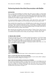
1.3inch OLED User Manual Waveshare 1.3inch OLED User Manual 1. Key Parameters Driver Chip SH1106 Interface Resolution 3-wire SPI、4-wire SPI、I2C 128*64 Display Size Dimension Colors Visible Angle 1.3 inch 29mm*33mm Yellow, Blue >160° Operating Temp. (℃) Storage Temp. (℃) -20~70 -30~80 Table 1: Key Parameters 2. Operation Description We will illustrate the usage of the module with an example of 4-wire SPI mode (default working mode) by connecting Waveshare Open103R development board (STM32F103R MCU on board). 1) Hardware configuration This module provides 3 kinds of driver interfaces; they are 3-wire SPI, 4-wire SPI and I2C interface. In its factory settings, BS0/BS1 pins are set to 0/0 and 4-wire SPI is selected as default. Different working mode and pin function of the module can be set by hardware selection on BS0/BS1 pins. (Notice: In this operation, welding is required. Any changes under no guidance from Waveshare will be considered as a waiver of warranty). symbol mode BS0/BS1 3-wire SPI 1/0 4-wire SPI 0/0 I2C 0/1 DIN CLK MOSI SCLK SDA SCL Table 2: Working mode setting 2) Software configuration Open the project file .\IDE\ OLED.uvproj in Keil, navigate to the following text, delete the ‘//’ (Double slash) before #define INTERFACE _4WIRE_SPI th V1.4.1, Feb. 26 2015 1 1.3inch OLED User Manual Waveshare After compiling successfully, download the project to Open103R development board. Note: You should delete the ‘//’ (Double slash) corresponding to the mode selection 3) Hardware connections Connect module to the SPI2 interface of Open103R development board, power up. OLED displays information as Figure 1 shows. Figure 1: OLED information display 3. 4-wire SPI and I2C interfaces of SH1106 OLED The 8080-Parallel Interface, 6800-Parallel Interface, Serial Interface (SPI) or I2C Interface can be selected by different selections of IM0~2 as shown in Table 3: . Table 3: Different selections of IM0~2 (SH1106_V2.3.pdf Chap. Functional Description) Note1: When Serial Interface (SPI) or I2C Interface is selected, D7~D2 is Hz. D7~ D2 is recommended to connect the VDD1 or VSS. It is also allowed to leave D7~ D2 unconnected. SH1106 provides 5 kinds of driver interfaces, however the OLED board just provides 3 kinds of driver interfaces settling (3-wire SPI, 4-wire SPI and I2C. the IM2 pin is set to “1” by hardware). BS0, BS1 correspond to IM0, IM1 respectively. We introduce 4-wire SPI and I2C interfaces here. Please read SH1106_V2.3.pdf for more details. th V1.4.1, Feb. 26 2015 2 1.3inch OLED User Manual Waveshare 3.1 4 Wire Serial Interface (4-wire SPI) The serial interface consists of serial clock SCL, serial data SI, A0 and CS . SI is shifted into an 8-bit shift register on every rising edge of SCL in the order of D7, D6, … and D0. A0 is sampled on every eighth clock and the data byte in the shift register is written to the display data RAM (A0=1) or command register (A0=0) in the same clock. See Figure 2: . Table 4: SPI interface setting (SH1106_V2.3.pdf Chap. 4 Wire Serial Interface) Note: “-” pin must always be HIGH or LOW. D7~ D2 is recommended to connect the V DD1 or VSS. It is also allowed to leave D7~ D2 unconnected. The serial interface is initialized when CS is high. In this state, SCL clock pulse or SDI data have no effect. A falling edge on CS enables the serial interface and indicates the start of data transmission. The SPI is also able to work properly when the CS always keep low, but it is not recommended. Figure 2: 4-wire SPI data transfer (SH1106_V2.3.pdf Chap. 4 Wire Serial Interface) When the chip is not active, the shift registers and the counter are reset to their initial statuses. Read is not possible while in serial interface mode. Caution is required on the SCL signal when it comes to line-end reflections and external noise. We recommend the operation be rechecked on the actual equipment. 3.2 I2C-bus Interface The SH1106 can transfer data via a standard I2C-bus and has slave mode only in communication. The command or RAM data can be written into the chip and the status and RAM data can be read out of the chip. th V1.4.1, Feb. 26 2015 3 1.3inch OLED User Manual Waveshare Table 5: I2C-bus Interface (SH1106_V2.3.pdf Chap. I2C-bus Interface) Note: “-” pin must always be HIGH or LOW. D7~ D2 is recommended to connect the V DD1 or VSS. It is also allowed to leave D7~ D2 unconnected. CS signal could always pull low in I2C-bus application. The I2C-bus is for bi-directional, two-line communication between different ICs or modules. The two lines are a serial data line (SDA) and a serial clock line (SCL). Both lines must be connected to a positive supply via a pull-up resistor. Data transfer may be initiated only when the bus is not busy. Note: The positive supply of pull-up resistor must equal to the value of VDD1. Bit Transfer One data bit is transferred during each clock pulse. The data on the SDA line must remain stable during the HIGH period of the clock pulse as changes in the data line at this time will be interpreted as a control signal. Figure 3: Bit Transfer (SH1106_V2.3.pdf Chap. I2C-bus Interface) Start and Stop conditions Both data and clock lines remain HIGH when the bus is not busy. A HIGH-to-LOW transition of the data line, while the clock is HIGH is defined as the START condition (S). A LOW-to-HIGH transition of the data line while the clock is HIGH is defined as the STOP condition (P). Figure 4: Start and Stop conditions Acknowledge Each byte of eight bits is followed by an acknowledge bit. The acknowledge bit is a HIGH signal put on the bus by the transmitter during which time the master generates an extra th V1.4.1, Feb. 26 2015 4 1.3inch OLED User Manual Waveshare acknowledge related clock pulse. A slave receiver which is addressed must generate an acknowledge after the reception of each byte. Also a master receiver must generate an acknowledge after the reception of each byte that has been clocked out of the slave transmitter. The device that acknowledges must pull-down the SDA line during the acknowledge clock pulse, so that the SDA line is stable LOW during the HIGH period of the acknowledge related clock pulse (set-up and hold times must be taken into consideration). A master receiver must signal an end of data to the transmitter by not generating an acknowledge on the last byte that has been clocked out of the slave. In this event the transmitter must leave the data line HIGH to enable the master to generate a stop condition. Figure 5: Acknowledge Protocol The SH1106 supports both read and write access. The R/W bit is part of the slave address. Before any data is transmitted on the I2C-bus, the device that should respond is addressed first. Two 7-bit slave addresses (0111100 and 0111101) are reserved for the SH1106. The least significant bit of the slave address is set by connecting the input SA0 to either logic 0(VSS) or 1 (VDD1). The I2C-bus protocol is illustrated in Figure 6: I2C Protocol. The sequence is initiated with a START condition (S) from the I2C-bus master that is followed by the slave address. All slaves with the corresponding address acknowledge in parallel, all the others will ignore the I2C-bus transfer. After acknowledgement, one or more command words follow which define the status of the addressed slaves. A command word consists of a control byte, which defines Co and D/C (note1), plus a data byte (see Figure 6: I2C Protocol). The last control byte is tagged with a cleared most significant bit, the continuation bit Co. After a control byte with a cleared Co-bit, only data bytes will follow. The state of the D/C -bit defines whether the data-byte is interpreted as a command or as RAM-data. The control and data bytes are also acknowledged by all addressed slaves on the bus. After the last control byte, depending on the D/C bit setting, either a series of display data bytes or command data bytes may follow. If the D/C bit was set to ‘1’, these display bytes are stored in the display RAM at the address specified by the data pointer. The data pointer is automatically updated and the data is directed to the intended SH1106 device. If the D/C bit of the last control byte was set to ‘0’, these command bytes will be decoded and the setting of the device will be changed according to the received commands. The acknowledgement after each byte is made only by the addressed slave. At the end of the transmission the I2C-bus master issues a stop condition (P). If the R/W bit is set to one in the slave-address, the chip will output data immediately after the slave-address according to the D/C bit, which was sent during the last write access. If no acknowledge is generated by the master after a byte, the driver stops transferring data to the master. th V1.4.1, Feb. 26 2015 5 1.3inch OLED User Manual Waveshare Figure 6: I2C Protocol th V1.4.1, Feb. 26 2015 6