1
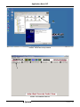
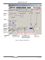
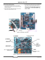
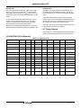
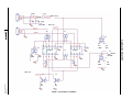
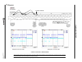
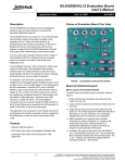
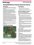
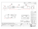
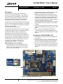
ISL45041EVAL1 User’s Manual ® Application Note Description The ISL45041EVAL1 is the evaluation board for the ISL45041 I2C LCD Module Calibrator. The evaluation kit comes complete with: ISL45041EVAL 1 board, DeVaSys USB to I2C converter board, USB cable to connect the converter board to a PC, Power and I2C cables for the ISL45041EVAL board and Software for both boards. The USB to I2C converter board (USB-I2CIO Rev B2) allows the user to adjust and program the ISL45041 VCOM voltage using a PC. For any help with the USB-I2CIO board please contact the manufacturer at http://www.devasys.com/usbi2cio.htm. This application note will guide the user through the process of installing the USB to I2C drivers, installing the ISL45041 Graphical User Interface (GUI) and configuring the ISL45041EVAL1 board for evaluation of the ISL45041. Additional equipment required are two power supplies, one volt meter and a PC (Windows 98/XP/2000 machine with a standard USB port). The board is designed to operate from an AVDD supply (5V-18V), and VDD supply (2.5V-3.6V). Installing the USB to I2C Drivers USB-I2CIO Board Driver Installation 1. The evaluation kit comes with a CD containing the software and drivers to control the I2C bus. Create a folder on your C drive called I2C_DCP and copy the contents of the CD to this folder. September 12, 2005 AN1207.0 2. After the files are copied, connect the USB cable to the USB port of a PC (it will power up the board). 3. Windows should detect the new USB device and the “Found New Hardware Wizard” should begin (as shown in Figure 2). This will help you install the drivers. Follow the directions on the screen until it asks you where to search for the drivers. At this point, you should select the “Search for a suitable driver for my device (recommended)” option and browse to the C:\I2C_DCP folder created in step one and select the drivers folder (.INF file). 4. Follow the remaining directions and the driver should be installed and the USB-I2CIO detected by your PC. Click finish. 5. Once the drivers are installed and the USB cable connected between the DeVaSys (USB-I2CIO) board and the PC, both LED’s on the board should be on (See Figure 1). Installing the ISL45041EVAL1 GUI 1. Open directory (C:\I2C_DCP), the one generated in the previous step. 2. Launch the “Intersil_IC2_DCP_ISL45041Eval.exe” File (as shown in Figure 2). When the first screen appears, click on the “Open USB” tab (as shown in Figure 3). 3. If the communication is established, the window should look like Figure 4 after clicking on the Open USB tab. In case of failed communication, the warning window will appear. FIGURE 1. USB-I2CIO BOARD (MADE BY DeVaSys) 1 CAUTION: These devices are sensitive to electrostatic discharge; follow proper IC Handling Procedures. 1-888-INTERSIL or 1-888-468-3774 | Intersil (and design) is a registered trademark of Intersil Americas Inc. Copyright Intersil Americas Inc. 2005. All Rights Reserved All other trademarks mentioned are the property of their respective owners. Application Note 1207 FIGURE 2. INSTALLING DeVaSys DRIVERS FIGURE 3. GUI SCREEN AT START-UP 2 AN1207.0 September 12, 2005 Application Note 1207 WARNING SIGNALS SELECTION REGISTER OR EEPROM WRITTEN DATA READ DATA SELECT FOR REPETITIVE WRITE OR READ CYCLES SETS INTERVAL TIME BETWEEN WRITE OR READ COMMANDS STOPS WRITE OR READ CYCLES SHOWS JUMPERS TO CONFIGURE THE ISL45041 WRITE MANUALLY (ALSO WRITTEN EVERY TIME THE POSITION IS CHANGED) READ THE REGISTER VALUE (COULD BE SELECTED TO READ BACK EVERY TIME THE REGISTER IS WRITTEN -- “AUTO READ” SET AND READ REGISTER POSITION FIGURE 4. GUI SCREEN TO PROGRAM ISL45041 3 AN1207.0 September 12, 2005 Application Note 1207 Connecting the Hardware 1. Connect the ISL45041EVAL1 board to the DeVaSys board as shown in Figure 5. Note: Connect the I2C cable as shown in Figure 5. 2. Set the VDD power supply (green wire) to 3.0V. Set the AVDD power supply (red wire) to 10.0V. 3. Connect the power supply cable to the ISL45041EVAL1 board. Note: Connect the power cable as shown in Figure 5. Turn on the power supplies to power up the ISL45041EVAL1 board (make sure the cables are connected properly -- RED = AVDD; GREEN = VDD; BLACK = GND). I2C CABLE POWER CABLE FIGURE 5. ISL45041EVAL1 TEST SETUP J10: SET RESISTOR SELECTION J16: SCL/SCL_C CLOCK INPUT SELECTION I2C CONNECTOR (SCL, SDA, GND) ISL45041IR OUTPUT VOLTAGE CAN BE OBSERVED ON J8 J5 AND J9: ISL45041 POWER SUPPLY (AVDD AND VDD) SELECTION POWER CONNECTOR (GND, AVDD, VDD) ISL45043 SOCKET J6 AND J7: EXTERNAL RESISTOR DIVIDER SELECTION J4: WPp POLARITY CONTROL (ISL45041) FIGURE 6. JUMPER SETTINGS FOR THE ISL45041EVAL1 BOARD 4 AN1207.0 September 12, 2005 Application Note 1207 Configuring the ISL45041EVAL1 Jumpers TABLE 1. VOUT HEX VALUE WRITING TO REGISTER HEX VALUE WRITING TO EEPROM 1 5.468 01 00 10 5.313 13 12 20 5.141 27 26 J4 is used for the Write Protect function test. To be able to program the part, J4 needs to be in the 1-2 position connecting the WP pin to VDD. The WP pin of the ISL45041 has an internal pull-down resistor. If J4 is open or in the 2-3 position (connecting this pin to GND) the part is write protected. 30 4.969 3B 3A 40 4.797 4F 4E 50 4.625 63 62 60 4.453 77 76 70 4.281 8B 8A J6 and J7 enable the user to change the external resistor values on the OUT voltage divider. To use the on board resistors (R13, R14) J6 and J7 need to be in the 2-3 position. To customize the output voltage the user can populate R11 and R12 with their desired resistor values and move J6 and J7 to the 1-2 position. 80 4.109 9F 9E 90 3.936 B3 B2 100 3.764 C7 C6 110 3.592 DB DA 128 3.282 FF FE Jumpers The board is equipped with jumpers to enable the user to adjust the SET current limit and values of output voltage with different values of R1 and R2 (reference schematic in Figure 7). Jumpers not used for the ISL45041 are J3, J6 and J16. These jumpers should be left open. J8 provides a convenient connection to monitor the VCOM output voltage. J10 enables the user to program the output current limit of the part. J10 needs to be in the 2-3 position to use the on board resistor R19. To customize the output current limit the user can populate R16 with their desired resistor value and move J10 to the 1-2 position. J5 and J9 provide the power to the ISL45041. SETTING VALUE Controlling the Output VCOM Voltage Using the GUI Figure 4 shows the Graphical User Interface for controlling the ISL45041EVAL1 board VCOM output voltage on jumper J8. The brief definition of the GUI’s application screen follows: I2C Slave Address You are now ready to adjust the VCOM output voltage using the ISL45041EVAL1 GUI. The I2C 8 bit Slave Address for this part is HEX code 9E or 9F. The I2C 7 bit Save Address for this part is HEX code 4F. Note the LSB sets the condition for writing to EEPROM (0) or Register (1). Reference Figure 8. Using the GUI to Control the VCOM Output Voltage Wrt - DATA - Rd Expected Output Voltage The ISL45041 provides an output sink current which lowers the voltage on the external voltage divider (VCOM output voltage). Equation 1 and Equation 2 can be used to calculate the output current (IOUT) and output voltage (VOUT) values. Setting AVDD IOUT = --------------------- X ----------------------------128 20 ( RSET ) EQ 1. R2 Setting R1 VOUT = ---------------------- AVDD 1 – --------------------- X ----------------------------- R1 + R2 128 20 ( RSET ) EQ 2. NOTE: Where setting is an integer between 1 and 128. Table 1 gives the calculated value of VOUT for the eval board using the on board resistors values of: RSET = 24.9K, R1 = 200K, R2 = 243K, and VADD = 10V. Also provided in Table 1 are the HEX values for several settings when writing to either the Register or EEPROM. 5 The Hex number displayed on the left is the logic string written to the ISL45041. The Hex number displayed on the right is the logic string read from the ISL45041. Once again, the LSB sets the condition for writing to EEPROM (0) or Register (1). This results in the first address being HEX 01 and the last being HEX FF when writing to the Register and 00 and FE when writing to the EEPROM (see Table 2). Clicking in the box to the right of the “Write Timer Controlled” or the “Read Timer Controlled”, will enable the user to select a time interval between Write or Read commands. Once you check the box the Stop Timer tab will appear. This will enable the automatic Write or Read cycle to stop. This feature is handy when evaluating the operation with a scope. For single Write or Read cycles click on the I2C-Write button or the I2C-Read button in the middle of the screen. Programming Mode Selects either the EEPROM or the Register to write to or read from. AN1207.0 September 12, 2005 Application Note 1207 Set Position Read Position This is how you adjust the ISL45041 output VCOM voltage. Placing your curser on top of the slide bar, click and hold then drag the mouse to adjust the VCOM voltage. When you release the mouse, the new HEX value will appear in the Wrt window. To read the value of the Register or EEPROM click on the I2C-Read button in the middle of the screen. This gives a visual representation of the either the EEPROM or Register value. The window directly below the slide bar shows the set bar position. The true decimal value of the logic code being written is one less than the number shown. This results because the ISL45041 has 128 resistive taps for programming. The digital logic designates 0 to 127 for the possible 128 steps. The slide bar starts at 1 and ends at 128. The window directly below the slide bar shows the bars position read from either the Register or EEPROM. The true decimal value of the logic code being read is one less than the number shown, for the same reason as above. Click on the auto read box in the bottom middle of the screen to automatically read any value selected. I2C Timing Diagram Figure 8 shows the I2C timing diagram and expected scope photos of SCL and SDA when writing all zeros or all ones. ISL45041EVAL1 Bill of Materials TABLE 2. ISL45041EVAL1 BOM PART NUMBER REF. DES. QTY H1046-00104-25V20 C13, C19-21 4 0.1µF 20% SMD-10% T353K106K050AS C15, C17 2 10µF 10% Radial-10% TANT-200 5000 TP 4 SIP 68000-236-1X3 J3-4, J6-7, J10, J16 4 1X3 Berg/FCI Connector/Header 68000-236-1X5 Power, I2C 2 1X5 Berg/FCI Connector/Header 69190-202 J5, J9 2 1X2 Berg/FCI Connector/Header H2512-01002-1/10W1-T R7-8 2 10K 1% 1/10W SMD-1% SM0805 Generic TFC Resistor H2512-02003-1/10W1-T R13 1 200K 1% 1/10W SMD-1% SM0805 Generic TFC Resistor H2512-02433-1/10W1-T R14 1 243K 1% 1/10W SMD-1% SM0805 Generic TFC Resistor H2512-02492-1/10W1-T R19 1 24.9K 1% 1/10W SMD-1% SM0805 Generic TFC Resistor ISL45041IR U7 1 TDFN 8DFN-3X3A Intersil Three Twisted Wire Male Banana Jack 1 +10V, +3V, GND 6 3 VALUE TOLERANCE POWER PACKAGE 1’ JEDEC SM0805 MANUF. DESCRIPTION Kemet Multilayer Capacitor Kemet Tantulum Capacitor CONN-GEN Keystone Mini Test Point VCOM Red, Green, Black Red, Green, Black AN1207.0 September 12, 2005 AVDD = 10.0V VDD = 3.0V 7 J16 J9 J6 J10 ISL45043 J5 R13 200K ISL45041 J8 VCOM OUTPUT R16 USER R19 24.9K VOLTAGE J7 R12 USER VDD = 3.0V J3 AN1207.0 September 12, 2005 R7 10K J4 R8 10K FIGURE 7. ISL45041EVAL1 SCHEMATIC R14 243K Application Note 1207 R11 USER I2C Diagrams 7 BIT ADDRESS 4 F 0 TO WRITE TO EEPROM 8 BIT ADDRESS 9 E 8 Application Note 1207 FIGURE 8. ISL45041EVAL1 TIMING DIAGRAM AN1207.0 September 12, 2005 Intersil Corporation reserves the right to make changes in circuit design, software and/or specifications at any time without notice. Accordingly, the reader is cautioned to verify that the Application Note or Technical Brief is current before proceeding. For information regarding Intersil Corporation and its products, see www.intersil.com