1
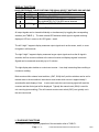
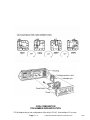
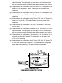
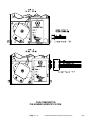
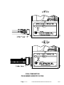
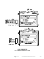
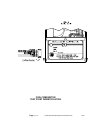
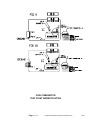
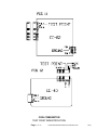
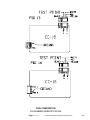
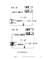
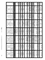
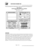
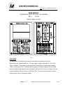
The Name in Validation Systems
PO Box 5128, 400 Regency Drive, Glendale Heights, IL 60139 FAX: (630) 924-7088 VOICE: (630) 924-7070
USER MANUAL
COMPARITOR TEST STATION P/N 00660003
REV. 1
6/19/99
FRONT PANEL LAYOUT
FIG. 1
OVERVIEW
The Comparitor Test Station can be used to test, adjust and troubleshoot all Coin
Mechanisms coin validation products. The input supply voltage is selectable to 110V, 120V,
220V, or 240VAC. The internal power supply can be externally set to three output voltages
12VDC, 24VDC and 24VAC. Switches can be toggled to simulate a machine’s inhibit control
lines and display output signals such as the sense, credit and tilt, and can be viewed on the two
numerical displays and as well as on a dual-color LED. The sensor coil null meter is used to
balance sensor coils on Comparitor models.
Page 1 of 15
G:\DOC\PROCED\0030\00300001R1\00300001.DOC
REV1
DISPLAY FUNCTIONS
QUICK REFERENCE TABLE POSITIONS FOR SIGNAL SELECT SWITCHES SW6 AND SW5
SW6
SW5
DISPLAY FUNCTIONS
UP×
UP×
CREDIT and LONG TILT PULSE WIDTHS
UP×
DOWNØ
SENSE PULSE WIDTHS
DOWN
UP×
SINGLE CREDIT PULSE WIDTHS and EVENT
Ø
also UNWANTED TILT PULSES can be detected
DOWN
DOWNØ
SENSE and CREDIT EVENT
Ø
Table 1
All output signals can be viewed individually or simultaneously by toggling the corresponding
switches (see TABLE 1). The dual-colored LED indicates which signal or signals are being
displayed, LED red = sense or tilt, LED green = credit.
The left 3-digit 7-segment display measures output signals such as the sense, credit, or some
tilt signals in milli-seconds.
The right 3-digit 7-segment display measures longer output signals such as the tilt signal in
seconds, the first counter overflows to the second counter and displays signals in seconds.
Signals can be measured accurately up to 15 minutes.
The right display also doubles as a coin/event counter. It can help in detecting false crediting or
numerous crediting.
Both counters utilize external reset switches, (SW7, SW4) the 3-position switches can be set for
manual reset or the test station’s internal auto-reset mode which occurs in approximately 2
seconds after each display of time. In auto-reset mode the next incoming signal will reset the
counters and then that signal will be displayed. Typically the manual reset (SW4) is used for
coin counting (accumulating), The milli-second counter reset switch (SW7) can typically run in
the auto-reset mode.
I / O HOOKUP FUNCTIONS
For simplified choices regarding operation of the test station refer to TABLE 1.
Page 2 of 15
G:\DOC\PROCED\0030\00300001R1\00300001.DOC
REV1
FRONT PANEL HOOK-UP: JP1
1 = SENSE input, sourcing signals only. (from sense output of Comparitor)
2 = OUTPUT VOLTAGE (pos. +) to Comparitor, selected via SW3 and controlled
via SW1. SW1 is used to switch power on or off only to the unit under test
connected to hot terminal 2 of JP1.
Caution: Care must be taken to ensure that the proper voltage range
is selected before connecting the unit to be tested.
3 = SENSE input, open collector signals only. (from sense output of
Comparitor)
4 = COMMON, GROUND
5 = CREDIT input, open collector signals only. (from credit output of
Comparitor)
6 = Micro-Switch N.O. connection only, (with internal debounce circuit)
Mechanical Mechs
micro-switch connection = N.O. tab to JP1 #6 and switch COMM. tab to JP1
#4.
7 = TILT input, open collector signals only. (from tilt output of Comparitor)
8 = INHIBIT output, controlled via SW2. (to inhibit input of Comparitor)
Switch SW1 is used to switch power on or off only to the unit under test
connected to hot terminal 2 of JP1
INHIBIT SWITCH
The Inhibit switch SW2 has marked settings on the front panel INH/HIGH, INH/FLT and
INH/LOW function as outlined below. The inhibit function output sends a signal level to the
Comparitor to disable it from accepting coins.
INH/HIGH =
12VDC, 24VDC or 15VAC
INH/FLT =
OPEN (Floating connection)
INH/LOW =
GROUND
To enable the Comparitor to accept coins (Comparitor Accept Mode) apply the proper signal
level to the inhibit wire, refer to Comparitor Specification Sheet.
SENSOR COIL NULL METER
JP2 = Comparitor Test Point, use banana/mini-clip lead and connect to Comparitors Test Point,
refer to schematic or Test Point identification at the end of this document. This test point is
typically used to view the null waveform on the null meter or oscilloscope.
VOLTAGE SELECTION
To change voltage: open cover, using small blade screwdriver or similar tool: set aside
cover/fuse block assembly: pull voltage selector card straight out of housing, using
Page 3 of 15
G:\DOC\PROCED\0030\00300001R1\00300001.DOC
indicator pin; orient selector card so that desired voltage is readable at the bottom; orient
REV1
COIN COMPARITOR
PIN NUMBER INDENIFICATION
FIG #1 depicts the pin out configuration of the six pin CC-46. Use interface “A” on units
Page 4 of 15
G:\DOC\PROCED\0030\00300001R1\00300001.DOC
REV1
with a JST header. This configuration can also apply to the CC-40 comparitors.
Refer to the machine manual to determine what outputs pertain to your machine.
Fig # 2 depicts the pin out configuration of the CC-33 and the CC-37 comparitors. Use
interface “B” with three pin JST header. The pin outs are the same for both
comparitors.
Fig # 3 depicts the pin out configuration of the CC-32 and the CC-36 comparitors. Use
interface “C” with six-pin MOLEX header. The pin outs are the same for both
comparitors.
Fig # 4 depicts the pin out configuration of the IC-33 and IC-37 with a JST header. Use
interface “A” on units with a JST header. The pin outs are the same on both
comparitors.
Fig # 5 depicts the pin out configuration for the IC-16. Use interface “C” with six-pin
MOLEX header.
Fig # 6 depicts the pin out configuration of the six pin CC-46. Use interface “A” on units
with a JST header. This configuration can also apply to the CC-16 comparitors.
Refer to the machine manual to determine what outputs pertain to your machine.
Fig # 7 depicts the pin out configuration for the seven pin CC-46. Use interface “D” on
units with a seven pin Molex header. This configuration can also apply to the
CC-62 or IC-62 comparitor.
Fig # 8 depicts the pin out configuration of the IC-32 and IC-36 with a JST header. The
pin outs are the same on both comparitors. Any additional pin out configuration
can be determined by referring to the specific comparitor specification
sheets.
COIN COMPARITOR
PIN NUMBER INDENTIFICATION
Page 5 of 15
G:\DOC\PROCED\0030\00300001R1\00300001.DOC
REV1
COIN COMPARITOR
PIN NUMBER INDENTIFICATION
Page 6 of 15
G:\DOC\PROCED\0030\00300001R1\00300001.DOC
REV1
COIN COMPARITOR
PIN NUMBER INDENTIFICATION
Page 7 of 15
G:\DOC\PROCED\0030\00300001R1\00300001.DOC
REV1
COIN COMPARITOR
PIN NUMBER INDENTIFICATION
Page 8 of 15
G:\DOC\PROCED\0030\00300001R1\00300001.DOC
REV1
COIN COMPARITOR
TEST POINT INDENTIFICATION
Page 9 of 15
G:\DOC\PROCED\0030\00300001R1\00300001.DOC
REV1
COIN COMPARITOR
TEST POINT INDENTIFICATION
Page 10 of 15
G:\DOC\PROCED\0030\00300001R1\00300001.DOC
REV1
COIN COMPARITOR
TEST POINT INDENTIFICATION
Page 11 of 15
G:\DOC\PROCED\0030\00300001R1\00300001.DOC
REV1
COIN COMPARITOR
PIN NUMBER INDENTIFICATION
Page 12 of 15
G:\DOC\PROCED\0030\00300001R1\00300001.DOC
REV1
COIN COMPARITOR
Page 13 of 15
G:\DOC\PROCED\0030\00300001R1\00300001.DOC
REV1
TEST POINT INDENTIFICATION
Page 14 of 15
G:\DOC\PROCED\0030\00300001R1\00300001.DOC
REV1
CC20,CC40,CC50
IC40
CC46
&
MC SERIES
Power / Tilt reset
CC61,CC62
DD62,2CC62&
IC62
Power ON/OFF
IC33,IC37
Power ON/OFF
IC-32,IC36
CC30 - series
TABLE 1
MATRIX
Power / Tilt reset
INF FLT = INHIBIT
(center position)
Power / Tilt reset
N/A
INH/LOW = ENABLE
(bottom position)
VOLTAGE
Refer to Spec Sheet
User preference
SENSE=
(bottom position)
Power ON/OFF
VOLTAGE
Refer to Spec Sheet
User preference
SENSE=
(bottom position)
N/A
CC10,CC16,
DD16HI12D
& IC16
VOLTAGE
Refer to Spec Sheet
User preference
SENSE = JP1 #3
(bottom position)
N/A
N/A
Power ON/OFF
VOLTAGE
Refer to Spec Sheet
User preference
SENSE =
(Refer to Spec Sheet)
CREDIT = JP1 #5
(top position)
N/A
EVENT
(bottom position)
SW1
CREDIT =
(Refer to Spec Sheet)
TILT = JP1 #7
(top position)
EVENT
(bottom position)
High or Low INHIBIT
Refer to Spec Sheet
VOLTAGE
Refer to Spec Sheet
User preference
NO SETTING
REQUIRED
CREDIT = JP1 #5
(top position)
TILT =
(Refer to Spec Sheet)
EVENT
(bottom position)
EVENT
(bottom position)
INF FLT = INHIBIT
(center position)
INH/LOW = ENABLE
(bottom position)
VOLTAGE
Refer to Spec Sheet
User preference
NO SETTING
REQUIRED
n/a
EVENT
(Refer to Spec Sheet)
EVENT
(bottom position)
N/A
N/A
n/a
n/a
TILT = JP1 #7
(top position)
For long Tilts also set
SW6 (top position)
EVENT
(bottom position)
EVENT
(bottom position)
N/A
INH FLT = INHIBIT
(center position)
n/a
EVENT
(bottom position)
EVENT
(Refer to Spec Sheet)
EVENT
(bottom position)
SW2
EVENT
(bottom position)
EVENT
(bottom position)
EVENT
(Refer to Spec Sheet)
INH/LOW = ENABLE
(bottom position)
VOLTAGE
Refer to Spec Sheet
User preference
n/a
EVENT
(bottom position)
EVENT
(bottom position)
N/A
n/a
N/A
n/a
(top position)
(top position)
User preference
PG 9 / FIG 10
1 = Sense, see Specs
2 = +Input Voltage
3 = Sense, see Specs
4 = Ground, common
5 = N/A
6 = N/A
7 = N/A
8 = Inhibit, see Specs
n/a
User preference
PG 9 / FIG 9
1 = Sense, see Specs
2 = +Input Voltage
3 = Sense, see Specs
4 = Ground, common
5 = N/A
6 = N/A
7 = N/A
8 = Inhibit, see Specs
n/a
INH/LOW = INHIBIT
(bottom position)
INH/FLT = ENABLE
(center position)
SW3
SW4
SW5
Sense
SW5
Credit
SW5
Tilt
SW6
Coin
SW6
Sense
SW6
Credit
SW6
Tilt
SW7
JP2
JP1
User preference
PG 10 / FIG 12
1 = n/a
2 = + Input Voltage
3 = n/a
4 = Ground, common
5 = Credit, low
6 = n/a
7 = Tilt, low
8 = Inhibit, see SW2
User preference
PG 10/ FIG 11
1 = Sense, see Specs
2 = +Input Voltage
3 = Sense, see Specs
4 = Ground, common
5 = Credit, see Specs
6 = n/a
7 = Tilt, see Specs
8 = Inhibit, see Specs
High going tilts to JP1#1
Low tilts are set
same as CC40 or
CC/IC62
User preference
PG 12 / FIG 15 & 16
1 = Sense, see Specs
2 = + Input Voltage
3 = Sense, see Specs
4 = Ground, common
5 = Credit, see Specs
6 = n/a
7 = Tilt, see Specs
8 = Inhibit, see Specs
User preference
User preference
PG 11 / FIG 13 & 14 PG 13 / FIG 17 &18
1 = SENSE, Sourcing 1 = SENSE, Sourcing
2 = +Input Voltage
2 = +Input Voltage
3 = n/a
3 = n/a
4 = Ground, common 4 = Ground, common
5 = n/a
5 = n/a
6 = n/a
6 = n/a
7 = n/a
7 = n/a
8 = Inhibit, see SW2
8 = n/a
See DD16HI12D Specs
G:\DOC\PROCED\0030\00300001R1\00300001.DOC
REV1
Page 15 of 15