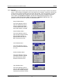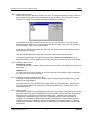
1
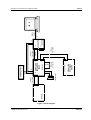
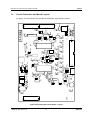
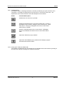
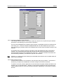
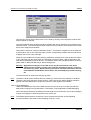
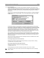
CML Microcircuits
COMMUNICATION SEMICONDUCTORS
EV8000
Evaluation Kit User
Manual
UM8000/4 October 2004
Provisional Issue
1.0
•
Features
For FX/MX828, 829 Product
Evaluation
•
Socketed Discrete Components
around Target Devices
•
UV-Erasable PIC µC Board
•
User's Prototyping Area
•
On-Board Microphone
•
Loudspeaker Output
•
On-Board Regulator
•
Single Power Supply Operation
•
Easy Access to Test Points
•
WindowsTM Software Included
1.1
Brief Description
The EV8000 Evaluation Kit comprises two boards. The signalling processor board contains an
FX828 and an FX829. The signalling processor board is powered from a single 8 - 35V dc power
supply; an on-board regulator sets 3.3V or 5.0V operation. LEDs indicate the status of the FX829
carrier detect output and the FX828 comparator output. Both of these lines are available on the
same connectors as the C-BUS. The FX828 and FX829 may be driven from a common external
clock, or from a common crystal oscillator. The supply current of either target device may be
measured by removing the appropriate jumper. A user prototyping area is provided and important
signals can be monitored by test points. There is an on-board microphone and a loudspeaker
output.
C-BUS signals can be applied at either of two connectors (J1 or J2). The other can be used to
add future C-BUS evaluation kits in parallel with the EV8000. A third connector (J3) provides a
daisy chained C-BUS to enable a second EV8000 signalling processor board to be controlled
from the same PC. The signalling processor board can also be used with a user's own µC board,
with appropriate software. Component footprints are provided in case the user requires level
shifting between the C-BUS input logic HI and the VDD level of the signalling processor board.
The µC board is fitted with a PIC µC containing the firmware to interface a PC serial port to the
signalling processor board C-BUS. The EV8000 is controlled by WindowsTM software on the PC.
© 2004 CML Microsystems Plc
Evaluation Kit User Manual for FX828 and FX829
EV8000
CONTENTS
Section
Page
1.0
Features ................................................................................................ 1
1.1
Brief Description ............................................................................... 1
1.2
Preliminary Information.................................................................. 4
1.2.1
1.2.2
1.3
Laboratory Equipment............................................................... 4
Handling Precautions ................................................................ 4
Quick Start ........................................................................................... 5
1.3.1
1.3.2
Setting-Up ................................................................................... 5
Operation .................................................................................... 6
1.4
Signal Lists .......................................................................................... 7
1.5
Circuit Schematics and Board Layouts................................. 12
1.6
Detailed Description ...................................................................... 14
1.6.1
1.6.2
1.6.3
1.6.4
1.6.5
1.6.6
1.7
Hardware Description - Signalling Processor Board ........... 14
Hardware Description - µC Board .......................................... 15
Software Description - Signalling Processor Board ............ 16
Software Description - µC Board............................................ 30
Known Bugs in the ES8000 (V 1.0) Software ........................ 31
Troubleshooting Guide for the ES8000 (V 1.0) Software ..... 32
Performance Specification ......................................................... 33
1.7.1
Electrical Performance ............................................................ 33
© 2004 CML Microsystems Plc
2
UM8000/4
© 2004 CML Microsystems Plc
EV8xxx
Loudspeaker
20-way
Flat Cable
3
J3
J1
SIGNALLING
PROCESSOR
BOARD
J1
Analogue
Connector
J6
J7
second (=far)
J5
(PCB004)
J2 SIGNALLING
PROCESSOR
BOARD
J4
POWER SUPPLY
20-way
Flat Cable
C-BUS
20-way
Flat Cable
J2
(PCB002)
µ C BOARD
J1
J4
J3
RS232
Cable
IBM - PC
Evaluation Kit User Manual for FX828 and FX829
EV8000
Figure 1 Block Diagram
UM8000/4
Evaluation Kit User Manual for FX828 and FX829
1.2
Preliminary Information
1.2.1
Laboratory Equipment
EV8000
The following laboratory equipment is needed to use this evaluation kit:
1.2.1.1 8 - 35V DC Power Supply (which can also be used to supply the PIC programming voltage, if set
to 13V).
1.2.1.2 A µC control board, together with appropriate firmware and a user interface. This kit contains a
suitable control board, which is fitted with a pre-programmed PIC 16LC74JW (or similar) µC.
1.2.1.3 An 8Ω loudspeaker.
1.2.1.4 An IBM compatible PC; 40MHz '386DX or better with 8MB of RAM, running Microsoft Windows
3.11 / '95 / NT having a serial port configuration of 8 data bits, no parity, 1 stop bit and 19,200
baud with hardware handshake but without CR -> CR/LF conversion.
The following laboratory equipment is needed to re-program the PIC µC in this evaluation kit:
1.2.1.5 If the evaluation kit is to be programmed via the serial port (J3), then a PC running DOS, or a
DOS window under Windows 3.11 or '95, will need to be used with the PIC programming software
supplied ( PICPROGA.EXE ).
1.2.1.6 As an alternative to on-board programming, a PIC 16-series Development System (available
from Arizona Microchip Technology), or a suitable PIC programmer, together with PIC
development software, may be preferred.
1.2.1.7 MPASM assembler or MPLAB software is required for re-assembling the source code. These
tools are available from Arizona Microchip Technology.
1.2.1.8 A UV-eraser to remove the pre-programmed PIC µC firmware.
1.2.2
Handling Precautions
Like most evaluation kits, this product is designed for use in office and laboratory environments.
The following practices will help ensure its proper operation.
1.2.2.1 Static Protection
This product uses low power CMOS circuits which may be damaged by electrostatic discharge.
Partially damaged circuits may function erroneously, leading to misleading results. Observe ESD
precautions at all times when handling this product.
1.2.2.2 Contents - Unpacking
Please ensure that you have received all of the items listed on the separate information sheet
(EK8000) and notify CML within 7 working days if the delivery is incomplete.
© 2004 CML Microsystems Plc
4
UM8000/4
Evaluation Kit User Manual for FX828 and FX829
1.3
EV8000
Quick Start
This section provides instructions for users who wish to experiment immediately with the
evaluation kit. A fuller description of the kit and its use appears later in this document.
1.3.1
Setting-Up
THE EV8000 COMES PRE-CONFIGURED FOR OPERATION AT 5.0V.
The µC board contains a socket for a 40-pin DIL PIC (or compatible) general-purpose µC, which
the user may re-program with his applications software. The µC board comes with a preprogrammed PIC 16C74AJW or equivalent containing communications firmware and application
specific demonstration firmware for the EV8000 evaluation kit.
The kit also contains a 9-way D-type RS232 cable (for connection to a PC), as shown in the Block
Diagram of Figure 1. No board adjustments are required by the user.
The C-BUS connector on the signalling processor board, J1 or J2, should be linked to connector
J1 on the µC board with a 20-way flat cable, as shown in Figure 1, connecting pin 1 to pin 1.
Analogue signals can be input or monitored at connector J6.
BEFORE APPLYING POWER, PLEASE CHECK THE FOLLOWING:
ENSURE THE PIC µC IS PLUGGED INTO SOCKET U2 ON THE µC BOARD.
ATTACH THE 9-WAY RS232 CABLE TO CONNECTOR J3 ON THE µC BOARD AND THE
SERIAL PORT OF A PC.
ATTACH THE 20-WAY FLAT CABLE TO CONNECTOR J1 ON THE µC BOARD AND
CONNECTOR J1 ON THE SIGNALLING PROCESSOR BOARD. PIN 1 MUST CONNECT TO
PIN 1.
Connect any other equipment as shown in Figure 1.
Ensure the PC software supplied is set up as detailed in Section 1.6.3.1.
The EV8000 boards each have connections for a single 8 - 35V dc power supply. Only one board
(as shown in Figure 1) needs to be connected as power is supplied to the other board over the
20-way flat cable. If the µC board supplied is not used, then power will need to be applied to the
signalling processor board instead. Each board has its own power supply regulator chip, with a
jumper to select 3.3V or 5.0V (default) operation.
Ensure that the component value jumpers on each of the EV8000 evaluation boards are correctly
set for 3.3V or 5.0V operation. Please refer to Sections 1.6.1.1 and 1.6.2.1 for further details.
MAKE SURE BOTH BOARDS HAVE THIS LINK SET TO THE SAME VOLTAGE. DAMAGE
MAY RESULT IF THIS STEP IS NOT OBSERVED. DO NOT OPERATE THE
µC BOARD WITH ITS VOLTAGE SELECTION LINK REMOVED. THE µC BOARD AND
SIGNALLING PROCESSOR BOARD VOLTAGE SELECTION LINKS HAVE DIFFERENT
CONFIGURATIONS.
© 2004 CML Microsystems Plc
5
UM8000/4
Evaluation Kit User Manual for FX828 and FX829
1.3.2
EV8000
Operation
This evaluation kit has no inherent functionality without the µC board and appropriate firmware
and PC software. The signalling processor board may be used independently of the µC board, if
the user wishes to interface to a different type of µC. The user will then have to supply his own
software.
The µC board is designed to control the operation of the signalling processor board. The
firmware which is pre-programmed into the PIC µC has both communications and application
specific functions. These functions are controlled from the PC software (ES8000) which runs in a
Windows environment.
Refer to Section 1.6.5 for the known software bugs and Section 1.6.6 for the troubleshooting
guide.
The PICPROGA.EXE program can be used to re-program the PIC µC firmware, if required.
© 2004 CML Microsystems Plc
6
UM8000/4
Evaluation Kit User Manual for FX828 and FX829
1.4
EV8000
Signal Lists
CONNECTOR PINOUT - SIGNALLING PROCESSOR BOARD
Connector
Ref.
Connector
Pin No.
Signal
Name
Signal
Type
J1, J2
1, 2
Power
+ve power from external power supply.
3, 4
VIN
VSS
Power
0V power from external power supply.
5
C-BUS-HI
I/P
Logic HI level for level shifting, if fitted.
6
D/IRQ
O/P
Alternative IRQ for daisy chain connector.
7
/IRQ
O/P
C-BUS interrupt line.
8
D/CS
I/P
Alternative CS for daisy chain connector.
9
/CS
I/P
C-BUS chip select line.
10
PTT
O/P
PTT switch.
11
SER-CLK
I/P
C-BUS serial clock.
12
I/O3
13
C-DATA
14
I/O1
15
R-DATA
16
I/O2
17
CARDET
O/P
FX829 carrier detect output.
18
COMPOUT
O/P
FX828 comparator output.
19, 20
VSS
1, 2
Power
+ve power from external power supply.
3, 4
VIN
VSS
Power
0V power from external power supply.
5
C-BUS-HI
I/P
Logic HI level for level shifting, if fitted.
6
VSS
D/IRQ
O/P
Alternative IRQ for daisy chain connector.
9
VSS
D/CS
I/P
Alternative CS for daisy chain connector.
10
I/O3
11
SER-CLK
I/P
C-BUS serial clock.
12
VSS
C-DATA
I/P
C-BUS command data.
VSS
R-DATA
O/P
C-BUS reply data.
J3
7
8
13
14
15
16
Description
Spare I/O
I/P
C-BUS command data.
Spare I/O
O/P
C-BUS reply data.
Spare I/O
Spare I/O
17
VSS
I/O1
Spare I/O
18
I/O2
Spare I/O
19, 20
VSS
© 2004 CML Microsystems Plc
7
UM8000/4
Evaluation Kit User Manual for FX828 and FX829
EV8000
CONNECTOR PINOUT - SIGNALLING PROCESSOR BOARD
Connector
Ref.
Connector
Pin No.
Signal
Name
Signal
Type
J4
1
Power
0V power from external power supply.
2
VSS
VIN
Power
+ve power from external power supply.
1, 2
SPEAKER
O/P
J5
Connector
Ref.
J6, J7
Description
Output for 8Ω loudspeaker.
CONNECTOR PINOUT - SIGNALLING PROCESSOR BOARD ANALOGUE INTERFACE
Connector
Signal
Signal
Description
Pin No.
Name
Type
even Nos.
1
VSS
MICIN
I/P
FX829 mic input.
3
829MOD2
O/P
FX829 MOD2 gain control output.
5
829MOD1
O/P
FX829 MOD1 gain control output.
7
AUDOUT
O/P
FX829 audio volume control output.
9
VOLIN
I/P
FX829 audio volume control input.
11
829MOD1IN
I/P
FX829 MOD1 gain control input.
13
829SUMOUT
O/P
FX829 audio summing amplifier output.
15
FFSK/DTMF
O/P
FX829 FFSK modem or DTMF gen output.
17
FILOUT
O/P
FX829 audio filter/limiter section output.
19
829EXTSUMIN
I/P
FX829 additional input to summing amp.
21
DEMODIN
I/P
FX829 Rx input.
23
COMPIN
I/P
FX828 comparator input.
25
8x8MOD2
O/P
FX828 MOD2 gain control output.
27
8x8MOD1
O/P
FX828 MOD1 gain control output.
29
TXSUBAUD
O/P
FX828 sub audio output.
31
8x8MOD1IN
I/P
FX828 MOD1 gain control input.
33
8x8SUMOUT
O/P
FX828 audio summing amplifier output.
35
TXAUDOUT
O/P
FX828 selcall tone generator output.
37
RXAUDOUT
O/P
FX828 Rx audio filter section output.
39
8x8EXTSUMIN
I/P
FX828 additional input to summing amp.
© 2004 CML Microsystems Plc
8
UM8000/4
Evaluation Kit User Manual for FX828 and FX829
EV8000
TEST POINTS - SIGNALLING PROCESSOR BOARD
Test Point
Ref.
Default
Measurement
TP1
8 - 35V
TP2
5.0V
TP3
0V
TP4
0V
TP5
0V
TP6
0V
VSS connection.
VSS connection.
TP7
LO
FX829 carrier detect output.
TP8
-
TP9
VDD/2
VDD/2
TP10
TP11
TP12
TP13
TP14
TP15
TP16
TP17
TP18
TP19
Description
VIN connection.
VDD connection (3.3V or 5.0V)
VSS connection.
VSS connection.
FX829 mic input.
FX829 DEMODFB pin.
FX828 RXAMPOUT pin.
VDD/2
VDD/2
FX829 MOD2 gain control output.
VDD/2
VDD/2
FX829 audio summing amplifier output.
FX829 MOD1 gain control output.
FX829 FFSK modem or DTMF generator output.
VDD/2
VDD/2
FX829 audio filter/limiter section output.
VDD/2
VDD/2
FX828 MOD1 gain control output.
FX828 MOD2 gain control output.
FX828 sub audio output.
TP20
VDD/2
VDD/2
FX828 audio summing amplifier output.
FX828 selcall tone generator output.
TP21
VDD/2
FX828 Rx audio filter section output.
TP22
-
TP23
HI
C-BUS interrupt request line.
TP24
HI
C-BUS chip select line.
FX828 comparator output.
JUMPERS - SIGNALLING PROCESSOR BOARD
Link
Ref.
Positions
Default
Position
JP1
1-2
o/c
Sets VDD = 3.3V (closed) or VDD = 5.0V (open)
JP2,3
1-2
1-2
Remove to supply an external clock to JP3 pin 2.
JP4
1-2
1-2
Remove to measure IDD of FX829.
JP5
1-2
1-2
Remove to measure IDD of FX828.
JP6
1-2 or 2-3
1-2
Select FX829 ( default ) or FX828 to drive loudspeaker.
JP7
1-2
1-2
Connects microphone to FX829 MICIN.
© 2004 CML Microsystems Plc
Description
9
UM8000/4
Evaluation Kit User Manual for FX828 and FX829
EV8000
CONNECTOR PINOUT - µC BOARD
Connector
Ref.
Connector
Pin No.
Signal
Name
Signal
Type
J1
1, 2
Power
+ve power from external power supply.
3, 4
VIN
VSS
Power
0V power from external power supply.
5
RA0
BI
PIC µC Bidirectional Port, pin 2
6
RA1
BI
PIC µC Bidirectional Port, pin 3
7
RA2
BI
PIC µC Bidirectional Port, pin 4
8
RA3
BI
PIC µC Bidirectional Port, pin 5
9
RB0
BI
PIC µC Bidirectional Port, pin 33
10
RB1
BI
PIC µC Bidirectional Port, pin 34
11
RB2
BI
PIC µC Bidirectional Port, pin 35
12
RB3
BI
PIC µC Bidirectional Port, pin 36
13
RB4
BI
PIC µC Bidirectional Port, pin 37
14
RB5
BI
PIC µC Bidirectional Port, pin 38
15
RB6
BI
PIC µC Bidirectional Port, pin 39
16
RB7
BI
PIC µC Bidirectional Port, pin 40
17
RC0
BI
PIC µC Bidirectional Port, pin 15
18
RC1
BI
PIC µC Bidirectional Port, pin 16
19
RC2
BI
PIC µC Bidirectional Port, pin 17
20
RC3
BI
PIC µC Bidirectional Port, pin 18
1
RA4
BI
PIC µC Bidirectional Port, pin 6
2
RA5
BI
PIC µC Bidirectional Port, pin 7
3
RD0
BI
PIC µC Bidirectional Port, pin 19
4
RD1
BI
PIC µC Bidirectional Port, pin 20
5
RD2
BI
PIC µC Bidirectional Port, pin 21
6
RD3
BI
PIC µC Bidirectional Port, pin 22
7
RD4
BI
PIC µC Bidirectional Port, pin 27
8
RD5
BI
PIC µC Bidirectional Port, pin 28
9
RD6
BI
PIC µC Bidirectional Port, pin 29
10
RD7
BI
PIC µC Bidirectional Port, pin 30
11
RE0
BI
PIC µC Bidirectional Port, pin 8
12
RE1
BI
PIC µC Bidirectional Port, pin 9
13
RE2
BI
PIC µC Bidirectional Port, pin 10
14 to 18 inc
-
-
19, 20
VSS
Power
J2
© 2004 CML Microsystems Plc
10
Description
Not used. No connection needed.
0V power from external power supply.
UM8000/4
Evaluation Kit User Manual for FX828 and FX829
EV8000
CONNECTOR PINOUT - µC BOARD
Connector
Ref.
Connector
Pin No.
Signal
Name
Signal
Type
J3
1
DCD
Output
PC connection (linked to DTR).
2
RXD
Output
PC connection to screen.
3
TXD
Input
PC connection to keyboard.
4
DTR
Input
PC connection.
5
Power
0V common connection to PC.
6
VSS
DSR
Output
PC connection (linked to DTR).
7
RTS
Input
PC 'RTS' connection.
8
CTS
Output
PC 'CTS' connection.
9
-
-
1
VSS
VIN
Power
0V power from external power supply.
Power
+ve power from external power supply.
J4
2
Description
Not used. No connection needed.
TEST POINTS - µC BOARD
Test Point
Ref.
Default
Measurement
TP1
8 - 35V
TP2
3.3V or 5.0V
TP3
0V
TP4
0V
TP5
3.3V or 5.0V
Description
VIN connection.
VDD connection.
VSS connection.
VSS connection.
VPP connection (13.0V in programming mode).
JUMPERS - µC BOARD
Link
Ref.
Positions
Default
Position
JP1
1-2 or 2-3
2-3
Sets VDD = 3.3V (1-2) or VDD = 5.0V (2-3)
JP2_1,2
1-2
1-2
Disconnect to supply external clock to JP2_1 (1).
JP3
1-2
1-2
Connects TXD to RS232 converter in normal use.
JP4 to JP7
1-2
n/f
Only fitted (and JP3 removed) in Programming Mode.
SW1
-
o/c
Push to reset switch. (Default = o/c = not reset).
Notes:
I/P = Input
Logic HI level
© 2004 CML Microsystems Plc
Description
O/P = Output
≈ +VDD
BI = Bidirectional
Logic LO level ≈ 0V (VSS)
11
UM8000/4
J2
© 2004 CML Microsystems Plc
VIN
12
VSS
TP5
J4
VDD
R27
TP1 C20
JP7
X2
C28
C26
U6
C27
JP4
R19
R5
JP1
R15
LK2
LK1
TP14
J5
JP6
1
1
1
MOD2 AUDOUT F/D
R23
TP25
MOD1 SUMOUT
U5
FILOUT
TP15
R14
C15
TP9
DEMFB
R16
LK4
C9
TP18
XX8x8
TP19
R11
TP20
TP21
C10 R8
C11
R9
LK3 R10
C7
J6
J7
R29
RXFB
R18
D4
S1
VSS
TP6
C32
J3
J1
PTT
1
1
CARDET COMPOUT
D3
R17
C12
R7
VSS
TP4
C25
C13 R28
R21
TP10
U4
C21
MOD1 SUMOUT TXAUD RXAUD
TP17
JP5
LK7
RP1
LK6
U3
LK5
MOD2 SUBAUD
TP16
C24
COMPOUT
R20 C8
TP22
C22 R22
C14
R12
TP24
/IRQ
TP23
C6 /CS
C2
R3
C16
XX829
R13
TP12
TP13
U2
TP11
MICIN
TP8
C19
C30 C17
CARDET
TP7
C4 JP3
C18
C23
R26
VDD
D2
C5 JP2
C3
R6
R25 U7
C31
X1
C1
TP2
R4
R1
74F07
VSS
1
VSS
R2
5
U1
4
D1
3
VIN
2
VSS
1
board mod
74HC4050
R24
1.5
TP3
Evaluation Kit User Manual for FX828 and FX829
EV8000
Circuit Schematics and Board Layouts
For clarity, circuit schematics are provided as a separate, high-resolution pdf file.
Figure 4 Signalling Processor Board - Layout
UM8000/4
Evaluation Kit User Manual for FX828 and FX829
D4
R1
R6
TP1 TP5
VIN
VPP
J1
EV8000
VSS
VIN
R3_2 R2_2
SW1
U1
C9
1
RD1
D2
C11
U2
PIC16C74
X1
C1
VSS
R4
JP5-7
D3
RS2
VDD
R5
RS1
R2_1 R3_1
D1
TP2
C10 TP4
1
RD2
JP1
1
C2
R8
J2
RD3
R7
JP2
1
C3
xclk
RD4
J3
JP3
JP4
C4
C5
MAX3232
C12
RS3
C6
C7
RS4
C8
U3
board mod
VSS
TP3
1
2
3
4
5
Figure 5 µC Board - Layout
© 2004 CML Microsystems Plc
13
UM8000/4
Evaluation Kit User Manual for FX828 and FX829
EV8000
1.6
Detailed Description
1.6.1
Hardware Description - Signalling Processor Board
1.6.1.1 Operating Voltage
Jumper JP1 is used to select the operating voltage. Open circuit selects 5.0V operation (default)
and closed circuit (link fitted) selects 3.3V operation.
1.6.1.2 Clock/Oscillator
The evaluation devices may use either an external clock or their own xtal oscillator. A 4.032MHz
xtal is provided on-board for the latter method. The links on jumpers JP2 and JP3, which are
normally fitted, select the xtal oscillator. An external clock may be supplied to JP3 pin 1 once the
links have been removed.
1.6.1.3 Microphone
By fitting a link to jumper JP7, the on-board electret microphone is connected via a buffer amplifier
to the MICIN input of the FX829. The signal applied to the FX829 can be monitored
at TP8. A push-to-talk (PTT) switch is also provided.
1.6.1.4 Loudspeaker
An 8Ω loudspeaker output is provided at the 3.5mm mono jack socket J5. The signal source for
the loudspeaker can be either the FX829 (default) or the FX8x8, link selectable at jumper JP6.
1.6.1.5 C-BUS and optional level shifting.
There are identical connectors (J1 and J2) either side of the board for C-BUS. This enables the
C-BUS source to be connected either side of the signalling processor board and also enables
future C-BUS evaluation boards to be connected in parallel. A third connector (J3) allows the
daisy chaining of a second signalling processor board with alternative /IRQ and /CS lines. This
allows for the emulation of both ends of a radio link, using a single PC.
If it is desired to operate the signalling processor board at VDD = 3.3V with the interface to C-BUS
operating at VDD = 5.0V, then level shifting components will need to be added to the signalling
processor board. Level shifting can be added to the C-BUS interface by removing solder links
LK4 to LK7 and fitting the following components:
A 74F07 in position U5.
A pull-up resistor pack in position RP1, suggested value 470Ω.
A pull-up resistor in position R22, suggested value 22kΩ.
A de-coupling capacitor for U5 may be fitted in position C22, suggested value 47nF.
1.6.1.6 Analogue re-configuration
Some discrete components and links around the target devices are socketed to allow path gains
to be adjusted. Also the analogue connector J6 has a second bare footprint, J7, which, in
conjunction with the removable components and links, can be used as a patch board to allow the
user to re-arrange signal paths as required.
1.6.1.7 IDD Measurement
The current consumption of the FX829 or the FX828 may be measured by removing the link on
jumper JP4 or JP5 respectively and replacing it with a multimeter.
© 2004 CML Microsystems Plc
14
UM8000/4
Evaluation Kit User Manual for FX828 and FX829
1.6.2
EV8000
Hardware Description - µC Board
1.6.2.1 Operating Voltage
Jumper JP1 is used to select the operating voltage. A link fitted at position 1,2 selects 3.3V
operation and at position 2,3 selects 5.0V operation (default). Do not operate this board with the
link on jumper JP1 removed.
1.6.2.2 Clock/Oscillator
A 4MHz xtal is the highest frequency xtal that may be used with a PIC16LC74(A)JW at
VDD = 3.3V. The PIC 16C74(A)JW has a similar limitation and is fitted for availability reasons.
Although rated at 5.0V, it has been found to work successfully at 3.3V. The links on jumpers JP2,
which are normally fitted, select an on-board 4MHz xtal. An external 3.58MHz clock, for
example, may be supplied to JP2_1 (1) once the links have been removed, taking care to adjust
any firmware timing routines accordingly.
1.6.2.3 RS232 Interface
The RS232 interface (connector J3) has its communications protocol determined by the µC
firmware. A suggested configuration is 8 data bits, no parity, 1 stop bit and 19,200 baud with
hardware handshake but without CR -> CR/LF conversion. The firmware supplied in the PIC µC
assumes this configuration.
1.6.2.4 Reset Switch (SW1)
This is provided to reset the PIC µC firmware, should this be required.
1.6.2.5 Programming Mode
TO ENTER PROGRAMMING MODE
(a)
(b)
(c)
(d)
(e)
(f)
(g)
Remove power from board
Disconnect the µC board from the signalling processor board
Ensure the link on jumper JP1 is fitted in position 2,3 for VDD = 5.0V
Remove link on jumper JP3
Insert links on jumpers JP4, JP5, JP6 and JP7
Re-apply power to board
Connect the programming voltage (VPP = 12.5V to 13.5V) power supply between test point
TP5 (+ve) and VSS (-ve)
(h) Ensure the PIC µC programming utility PICPROGA.EXE is loaded into the PC under DOS
and the PC is connected to the µC board
(i) UV-erase the PIC µC first, then download firmware into the PIC µC and verify it
TO LEAVE PROGRAMMING MODE
(a)
(b)
(c)
(d)
(e)
Remove power from board (including the programming voltage)
Remove links on jumpers JP4, JP5, JP6 and JP7
Insert a link on jumper JP3
Reconnect the link on jumper JP1 to its original position
Reconnect the µC board to the signalling processor board, checking that the voltage
selection jumpers are correctly set
(f) Ensure the ES8000 software is running on the PC under Windows
(g) Re-apply power to board and run the new µC firmware
© 2004 CML Microsystems Plc
15
UM8000/4
Evaluation Kit User Manual for FX828 and FX829
1.6.3
EV8000
Software Description - Signalling Processor Board
1.6.3.1 Installation
The ES8000 Windows Application Software consists of a single executable file named
ES8000xx.EXE, where xx refers to the version number. Copy this from its 3.5” floppy disk to the
hard disk of the user’s PC.
Windows NT and '95
For convenient and quick launching of the program create an ES8000 shortcut within the Start
menu or Desktop.
Windows 3.11
For convenient and quick launching of the ES8000 software create a new program group and
ES8000 icon.
1.6.3.2 System Requirements
This program is a 16-bit application, compatible with Windows 3.11, NT and '95 operating
systems. The software has been designed to operate on a 386DX 40MHz or faster with 8MB of
RAM. We recommend that the user has the screen resolution set no lower than 800 x 600, to
allow maximised device forms to fit within the screen.
Note:
ES8000 Version 1.0 requires the signalling processor board crystal (X1) frequency to be
4.032MHz, to ensure correct generation of frequency data.
1.6.3.3 Starting the ES8000 Windows Application Software
Windows NT and '95
To execute the program from the Start Menu click on the Start Button, and then point to the
folder that contains the ES8000 Windows Application Software. Click on the program when it has
been located.
If a shortcut has not been created in the Start Menu then execute the program using the Run
command, click on the Start button and then click on Run. Type the path and name of the
program and then click on the OK button. If the program path is unknown click on Browse to look
for the item.
Windows 3.11
To execute the program locate the ES8000 icon from the appropriate program group. Double
click on the program icon when it has been located.
If a program group and icon has not been created execute the program using the Run command,
click on the File menu then click on Run. Type the path and name of the program and then click
on the OK button. If the program path is unknown click on Browse to look for the item.
1.6.3.4 Shutting Down the ES8000 Windows Application Software
Windows NT and '95
To quit the ES8000 program click on the close button in the upper-right corner of the main
application window.
Windows 3.11
To quit the ES8000 program click on the upper-left corner pulldown application menu, click on
the close command.
© 2004 CML Microsystems Plc
16
UM8000/4
Evaluation Kit User Manual for FX828 and FX829
EV8000
1.6.3.5 Near and Far ES8000 Definitions
The near EV8000 signalling processor board is connected to the µC board via the J1 connector.
Therefore all FX8xx devices located on the near signalling processor board are considered to be
near devices and are controlled by near device forms.
The far signalling processor is created by taking a signalling processor board out of a second
EV8000 evaluation kit. It should be connected to the near signalling processor board by using
another 20-way flat cable between connector J3 on the near board and connector J1 on the far
board. Pin 1 on connector J3 should be connected to Pin 1 on connector J1. All FX8xx devices
located on the far signalling processor board are considered to be far devices and are controlled
by far device forms.
Note:
In certain parts of the ES8000 Windows Application Software the variables CBUS and CBUS2 are
used. These correspond to the near and far boards respectively.
1.6.3.6 ES8000 and EV8000 Startup Procedure
Ensure all of the hardware is connected correctly. Follow the ‘Starting the ES8000 Windows
Application Software’ instructions described earlier. When the ES8000 Windows Application
Software is executed a pop-up window asks the user to switch on the EV8000 kit. Switch on the
power supply feeding the signalling processor and µC boards.
When power has been applied the Add Device pop-up window is opened. If the user is ready to
add a device form to the view select the device and click on OK. Click on cancel if you do not
require a device form.
Perform a General Reset when the first device form is opened, any further device forms added
will not require a General Reset unless they have been opened on the other C-BUS (near or far).
If the ES8000 Windows Application Software is executed with power already applied to the
signalling processor and µC boards, simply press the reset switch (SW1) on the µC board. The
Add Device window should now open.
If these methods fail, shutdown the ES8000 application and turn off the power supply to the
signalling processor and µC boards. Repeat the procedure described above.
© 2004 CML Microsystems Plc
17
UM8000/4
Evaluation Kit User Manual for FX828 and FX829
EV8000
1.6.3.7 Toolbar Buttons
An ES8000 toolbar, containing five buttons, has been provided to give quick access to menu
commands. The toolbar is optional and can be turned on or off from the View menu. The
appearance of the buttons and their command descriptions are as follows:
Button
Command Description
Initialises the Com link to the µC board
Notifies the software that the user will be resetting the µC board. It
generates a pop-up window, asking the user to push the µC board
reset switch. This pop-up disappears when the µC board reset
switch (SW1) is pushed.
Performs a General Reset on the current C-BUS. All EV8000
devices and ES8000 active device forms on this C-BUS will be
reset.
Opens the Add Device pop-up window.
Opens the About ES8000 pop-up window which displays program
information and version number.
1.6.3.8 Viewing the Toolbar and Status Bar
The Toolbar and Status Bar can be removed from or inserted into the main window by clicking on
the View menu and then clicking on the required command.
© 2004 CML Microsystems Plc
18
UM8000/4
Evaluation Kit User Manual for FX828 and FX829
EV8000
1.6.3.9 Menubars
The main application menubar which resides at the top of the main window contains five pulldown
menus. This menubar is available for use until a device form is opened. Whenever a device form
is active a form menubar resides at the top of the main window. This form menubar is currently
the same for all devices and is similar to the main menubar except for an additional pulldown
menu called Local (disabled in Version 1.0) and three additional Global pulldown menu
commands called General Reset, BER Test and Demo1 (disabled in Version 1.0). The
pulldown menus from the form menubar are illustrated below.
Setup Pulldown Menu
This menu allows the user to
open the Add Device pop-up
window, initialise the RS232
communications link to the µC
board and reset the µC board.
Global Pulldown Menu
This menu allows the user to
open the Direct C-BUS Control
pop-up window, perform a
General Reset and open the
BER Test pop-up window.
View Pulldown Menu
This menu allows the user to
turn the Toolbar and Statusbar
on or off.
Window Pulldown Menu
This menu allows the user to
rearrange iconised or opened
device forms and to switch
between the device forms.
Help Pulldown Menu
This menu allows the user to
open the About ES8000 pop-up
window which displays program
information and version number.
© 2004 CML Microsystems Plc
19
UM8000/4
Evaluation Kit User Manual for FX828 and FX829
EV8000
1.6.3.10 Adding a Device Form
There are two ways to add device forms to the view. The quickest method is to click on the Add
Device toolbar button which opens the Add Device pop-up window. The second way involves
clicking on the Setup menu and then selecting the Add Device command.
The Add Device window gives the user the choice of near and far devices. The user should
select the required device form corresponding to the device located in the near or far signalling
processor board. Finally, click on the OK button.
If a device form already exists within the main view, this selection will not be available from the
Add Device pop-up window.
The cancel button allows the user to exit the window without selecting a device form.
If the user attempts to open more than four device forms (Version 1.0 maximum) during an
evaluation session, a pop-up window will notify the user that no more device forms are available.
1.6.3.11 Deleting a Device Form
Windows NT and '95
To close a device form (iconised or open), click on the close button in the upper-right corner of the
device form.
Windows 3.11
To close a device form (not iconised), click on the upper-left corner pulldown menu of the device
form, and click on the close command.
1.6.3.12 Switching between Opened Device Forms
A device form must have the focus to allow the user to modify the Write registers and view the
settings of the read registers.
The device form focus can be switched by simply clicking on the required form. Switching the
focus can also be achieved by clicking on the Window pulldown menu, and then click on the
required device form.
1.6.3.13 Device Forms
The evaluation software has been designed so that each device has a corresponding device form.
The device forms have been created based on the device data sheets to allow the user to easily
and quickly set up a device in the required operating mode. Additional FFSK sections are
included on the FX829 device form, as it was considered important to have these features
available. Future releases of the ES8000 software will include device demonstration windows.
The device forms for the FX828 and FX829 are illustrated on the following pages. It should be
noted that this evaluation kit will also support an earlier device, the FX818, which has now been
discontinued.
© 2004 CML Microsystems Plc
20
UM8000/4
Evaluation Kit User Manual for FX828 and FX829
EV8000
FX828
Note:
The GP Timer edit box displays the number to be programmed into the GP Timer Register.
© 2004 CML Microsystems Plc
21
UM8000/4
Evaluation Kit User Manual for FX828 and FX829
EV8000
FX829
For certain user input values, device programming data will not be generated and the write
register concerned will not be updated. When this situation occurs a stop error message pop-up
window will be opened to notify the user. The user should then re-enter a new value before
clicking on the Update button.
Other (incorrect) user input values may be entered, causing the application to open an information
pop-up window. This window notifies the user that the device write register was programmed, but
with invalid data.
© 2004 CML Microsystems Plc
22
UM8000/4
Evaluation Kit User Manual for FX828 and FX829
Note:
EV8000
The ES8000 Windows Application Software can be used to evaluate FX828 and FX829 devices
outside their specified characteristics. Therefore, minimum and maximum device form input
values used within the application are based on the validity of the equations used to generate the
programming data and register size constraints,
ie. An 8-bit register allows an integer input of 0-255.
1.6.3.14 Writing and Reading the FX828 and FX829 device registers
When the write register of a device form has been set up, the settings can be loaded into the
appropriate device by clicking on the Update button. This will also acquire the settings of the read
registers. The read register settings will then be displayed on the device form view. To minimise
data exchange between the PC and EV8000, only modified write register settings are passed to
the µC.
1.6.3.15 Write Register Input Controls
The device forms have been created to allow the user to quickly and easily set-up the device write
registers.
Checkboxes are used for the majority of write register input controls. Each checkbox usually
corresponds to a data bit in a write register. The write register bit is set to ‘1’ when the checkbox
is checked and set to ‘0’ when unchecked. The toggling between checked and unchecked is
achieved by clicking on the checkbox area.
Due to variations in the Windows libraries, the checkbox display on a Windows 3.11 operating
system will have a different appearance to that on Windows NT and '95. The differences in
display on the various Windows platforms are as follows:
Windows NT and '95
The checkbox will have a 3D appearance with a 9 (tick) indicating the checkbox is checked (Bit
set to ‘1’). The inside of the checkbox is a different colour to the form foreground colour. Note: if a
checkbox is ever disabled by the software, the inside of the checkbox will be greyed together with
the checkbox description text. Once disabled the user cannot change the state of the checkbox.
Windows 3.11
The checkbox will have a 2D appearance with a X (cross) indicating the checkbox is checked (Bit
set to ‘1’). The inside of the checkbox is the same colour as the form foreground colour. Note: if
a checkbox is ever disabled by the software, the inside of the checkbox remains the same colour
but the checkbox description text will be greyed. Once disabled, the user cannot change the state
of the checkbox.
To enter frequencies, integer values and codes, edit boxes are provided. The user should click
on an edit box and enter the required value. If the input value is outside the evaluation limits or
the format of data is invalid, an error or warning pop-up window message will be encountered
when the Update button is clicked.
To select from a list of settings, dropdown lists (combo boxes) and vertically scrolled multiline edit
boxes are provided.
© 2004 CML Microsystems Plc
23
UM8000/4
Evaluation Kit User Manual for FX828 and FX829
EV8000
The user should click on the drop button located to the right of the combo box. When the combo
box opens up, the vertical scroll bar should be used to move up and down through the list of
options. When the required option is found, the user should click on it. Likewise, for the multiline
edit boxes, the list of options can be viewed and selected by using the vertical scroll bar followed
by clicking on the option.
1.6.3.16 Read Register Output Display
The read register output display section located on the right of the device forms consists of readonly single line edit boxes. These boxes display the read register settings after an update or View
Register has taken place. The edit boxes corresponding to bit settings will display either the
‘clear’ or ‘set’ text corresponding to a ‘0’ or ‘1’ respectively.
1.6.3.17 FX828 Rx Tones
The FX828 device forms are very similar for the entry of Rx tones. However, the multiline edit
box list created for the FX828 will display CTCSS and Selcall tones, depending on the state of the
Tone Decoder Mode bit in the Signalling Set-up write register. For the FX828, both sets of tones
are stored in memory but only one set is sent to the EV8000 Evaluation Kit, depending on the
Tone Decode mode setting.
Assigning frequencies to an Rx tone is achieved by clicking on the required tone number and then
entering the frequency in the single line edit box on the right. No enter key or delimiter is required
at the end of the frequency setting. When the tone number is selected the focus automatically
switches to the frequency edit box ready for frequency entry.
1.6.3.18 Viewing the FX828 and FX829 device registers
The current device form write register settings and the actual device read register settings can be
viewed by clicking on the View Registers button. The pop-up window which follows, lists the
register addresses and data.
To allow the user to view all of the FX828 CTCSS/Selcall tones, dropdown edit boxes are
included in the FX828 View Registers’ windows.
© 2004 CML Microsystems Plc
24
UM8000/4
Evaluation Kit User Manual for FX828 and FX829
EV8000
1.6.3.19 Automatic Disabling of Input Controls
This software feature shows the user which areas of the device form require user input and also
prevents the user selecting incorrect modes of operation.
An input control disabled by the software will be greyed on the display and will not respond to the
user clicking on it. When the software establishes that the user has modified an input control,
thus eliminating any possible conflicts, the disabled input control will be re-enabled, ready for user
selection.
An example of the conflicting modes of operation is when the FX828 Sub-Audio Transmitter is
enabled. The FX828 data sheet states that the DCS decoder and the Sub-Audio (CTCSS or
DCS) transmitter should not be enabled at the same time. Therefore the DCS Rx checkbox will
be automatically disabled by the software to prevent user selection.
Note:
Windows 3.11 users may find the display text associated with edit boxes to be invisible whilst the
input control is disabled.
1.6.3.20 Direct C-BUS Control
Individual device registers can be written to and read using this pop-up window. The window is
activated by clicking on the Global Menu and then clicking on the C-BUS command.
To perform a write to a device register the user should enter the register address and data in hex
and then click on the Write button. Likewise, to read a device register the user should enter the
register address and then click on the relevant read button, depending on the number of bytes to
be read.
© 2004 CML Microsystems Plc
25
UM8000/4
Evaluation Kit User Manual for FX828 and FX829
EV8000
The user can read or write to either near or far C-BUS by clicking on the respective C-BUS radio
buttons (CBUS or CBUS2).
The General Reset button within this window will allow the user to reset devices controlled by the
selected C-BUS. The General Reset button within the Direct C-BUS Control window will not reset
device form displays and variables.
This window contains an interrupt notification section. This section comprises of two checkboxes
to select either near or far C-BUS interrupts and two corresponding multiline read-only edit boxes
to display the source of the interrupts.
When the user enables one of these interrupt notification checkboxes, the PC will then be notified
of any interrupts from the (near and/or far) signalling processor boards. IRQ corresponds to the
near devices and IRQ2 to the far devices. The interrupt source string displayed shows the device
(either x829 or x828) and IRQ Flag or Status setting (Hex).
Warning: Application warnings or even fatal errors may be encountered if the Direct
C-BUS Control window is used to view interrupt notifications that are occurring
less than every 10ms. Whilst viewing continuous interrupt notifications the user
should disable the Windows Screen Saver and not attempt any window resizing,
etc.
The Cancel button is used to exit this pop-up panel.
Note:
The Direct C-BUS Control window does not modify any of the device form displays or variables.
Therefore, after using the Direct C-BUS Control, certain device form display settings should be
ignored until a General Reset is performed or the form write registers are modified.
1.6.3.21 FFSK Messaging
Unlike the FX828 device forms the FX829 device forms can be set up to receive and transmit
data without clicking on the Update button. This feature is only applicable to FFSK Messaging.
Due to the speed constraints of Windows and the serial communication link, the FFSK messaging
routines controlling the FX829 are performed by the PIC µC.
Note:
The EF8000 firmware does not allow the user to operate both the near and far signalling
processor boards in the same FFSK messaging mode (Tx or Rx).
© 2004 CML Microsystems Plc
26
UM8000/4
Evaluation Kit User Manual for FX828 and FX829
EV8000
1.6.3.22 FFSK Rx Message
Select FFSKRX and AMP1 by clicking on their respective checkboxes in the Control 1 write
register and enable the required synchronisation bit in the Control 3 / IRQ Enable write register. If
RX SYNC WORD PRIME is selected, enter a 2-byte RX SYNC word in hex, before clicking on the
Update button. If required, other control bits can be set before the Update button is clicked i.e.
baud rate, etc.
The user can now setup the FFSK Rx Message section of the device form. Start by entering the
number of data bytes in a single message, click on the Rx Bytes edit box and enter an integer
number(1-11).
If a FFSK Rx checksum is required based on the number of bytes expected, the Rx checksum
should be set by checking this checkbox. The FFSK Rx message setup can be stored in memory
at any stage by clicking on the Update button. To transfer the data to the µC board and thus start
receiving FFSK messages the user should click on the Rx Message Start button. The FFSK
message received will be displayed in the read-only, multiline, vertically scrolled edit box. This
edit box will clear automatically when a maximum number of lines is reached (500) . However a
clear button is provided to allow the user to clear the edit box at any stage.
Up to 15 following words can be received by the FFSK Rx Message section, by clicking on the
appropriate edit box and entering the required number. A following word comprises of message
data bytes and checksum (if transmitted) immediately following the previous message without
further synchronisation.
Whilst receiving FFSK messages the FFSK Rx Message Start button is disabled until the FFSK
Rx Stop button is clicked by the user.
Rx message display format with Rx checksum:
Message Synchronisation Codeword, D(message data bytes), C(2-byte checksum, validity)
i.e. SYNC, D(AA,11,33), C(85,2A, TRUE)
Rx message display format without Rx checksum:
Message Synchronisation Codeword, D(message data bytes)
i.e. WORD, D(AA,11,33)
The Rx Message Synchronisation Codeword will be either SYNT, SYNC or WORD.
Note:
The FX829 device form cannot receive continuous FFSK messages when the inter-message
delay is <100ms.
© 2004 CML Microsystems Plc
27
UM8000/4
Evaluation Kit User Manual for FX828 and FX829
EV8000
Warning: Prolonged window resizing or similar background activities may cause
application warnings or even fatal errors whilst receiving continuous FFSK
messages with small inter-message delays.
1.6.3.23 FFSK Tx Message
Select FFSKTX, TXIDLEM and TXDATAM by clicking on their respective checkboxes and then
click on the Update button. If required, other control bits can be set before Update button is
clicked i.e. baud rate etc.
The user should then enter the number of data bytes to be transmitted in a single message using
the Tx message bytes edit box (2-9). The number of preamble bytes should be entered into the
preamble bytes edit box (2-15). The user has the option of adding a 2-byte checksum to the
message. This can be achieved by checking the Tx Checksum checkbox.
The FFSK Tx message form setup can be stored in memory at any stage by clicking on the
Update button. To transfer the data to the µC board and therefore transmit the FFSK message,
the user should click on the Tx Message Start button.
A checkbox is provided to allow the user to continuously transmit the same FFSK message.
When this checkbox has been checked the user has the option of re-transmitting the 2-byte
synchronisation code. When the Re-Transmit Sync checkbox is checked an inter-message delay
can be specified. The minimum message delay is 100ms, although a value of 0 can be entered to
indicate that no delay is required.
In continuous Tx mode the transmission can be stopped by clicking on the Continuous Tx Stop
button. To indicate that a continuous FFSK transmission is in progress the Tx Message Start
button is disabled until the Continuous Tx Stop button is clicked by the user. Likewise when the
Continuous Tx checkbox is unchecked the Re-Transmit Sync checkbox and Message Delay edit
box are disabled.
Note:
The timer used for the inter-message delay has been implemented in the Windows software.
Therefore, the delay may vary depending on PC performance and other background tasks
running. Whilst operating in continuous FFSK Tx mode with an inter-message delay, it is
recommended that the user disables the Windows Screen Saver and does not attempt any
window resizing, etc.
In continuous FFSK transmit mode with an inter-message delay specified, the delay entered by
the user is the time difference between the end of a message and the start of the next message.
© 2004 CML Microsystems Plc
28
UM8000/4
Evaluation Kit User Manual for FX828 and FX829
EV8000
1.6.3.24 FX829 Bit Error Rate Testing
To allow the user to perform FX829 Bit Error Rate Testing (BERT) the EF8000 firmware contains
a BERT routine, configured by the ES8000 Windows Application software. This facility requires
two EV8000 signalling processor boards (near and far) and user input to both near and far FX829
device forms before BERT can commence.
Hardware Setup
This function enables connection to a BER Testers as follows:
µC Board J2 Pin 1 to Tester Tx Data O/P
µC Board J2 Pin 2 to Tester Tx Clock I/P
µC Board J2 Pin 3 to Tester Rx Data I/P
µC Board J2 Pin 4 to Tester Rx Clock I/P
The Tester must be able to operate from an external clock. The timings of the clocks provided
from the µC board are as follows:
Rx Clock
1 Byte Time
tA
Tx Clock
1 Byte Time
tB
Times tA and tB vary as the clocks are adjusted to fit the exact byte periods of the target devices.
Data is assumed to be clocked in and out of the Tester on the rising edge of either Rx or Tx clock.
The FX829 FFSK data from the transmitting signalling processor board can be directly fed from
FFSK/DTMF Out (J6 Pin 15) into noise summing circuitry, or via one of the FX829 modulator
paths. The output of the noise summing stage should be connected into DEMODIN (J6 Pin 21) of
the receiving signalling processor board.
Application Software Setup
After executing the ES8000 Windows Application software the user should open the near and far
FX829 device forms. Select FFSKTX, TXIDLEM and TXDATAM on the device form used to
control the transmit end. Other write register bits may need to be enabled if the user is not
transmitting directly from FFSK/DTMF Out (J6 Pin 15). On the device form used to control the
receive end, select FFSKRX, AMP1 and one of the required synchronisation primes.
When the near and far FX829 device forms have been configured select the BER Test command
from the Global pulldown menu. The BER Test pop-up window will now appear with a read-only
edit box providing status information on the BER Test.
© 2004 CML Microsystems Plc
29
UM8000/4
Evaluation Kit User Manual for FX828 and FX829
EV8000
Two control buttons allow the user to start and stop the function which in turn generate either
‘running’ or ‘idle’ status messages.
The Tester should be started before the user clicks on the Start button to ensure bit
synchronisation is achieved.
Error messages will be reported in the status edit box if the user has incorrectly configured the
FX829 device forms.
Note:
Other device functions should not be performed whilst the BERT facility is operational.
1.6.4
Software Description - µC Board
1.6.4.1 PIC µC Programming Software
This is supplied on disk as a self-documented executable file PICPROGA.EXE for a PC running
DOS (either directly or as a DOS window in Windows 3.11 or '95). It is not recommended for use
on Windows NT systems. Please note that this programming software does not meet the Arizona
Microchip Technology verification requirements for a "production quality" programmer. Also, it
does not support the programming of ID locations and there is no checksum facility.
The user interface consists of two windows. The top window contains the operating instructions
and the bottom window shows the command line and data communications with the PIC µC.
When the top window first appears the user will be prompted to enter the number of the serial
communications port to which the µC board is connected. Once the user has entered this
number, the following commands are displayed:
press F
to load file.
press C
to enter Configuration Word.
press B
to check target device is blank.
press P
to program target device.
press V
to verify target device.
press R
to read target device.
press A
to view contents of program data array.
Currently - xxxx
press Esc to return to DOS.
A new function from the above table can be selected whenever the >ok prompt appears in the
bottom window.
© 2004 CML Microsystems Plc
30
UM8000/4
Evaluation Kit User Manual for FX828 and FX829
EV8000
Notes:
a)
Assembler output files must be in the Intel hex format (.HEX) in order to be usable by this
programming software.
b)
The PIC µC supplied has a Configuration Word which is preset to 3FB9H if it is a PIC
16C74JW or 16LC74JW, or to 3FB1H if it is a PIC 16C74AJW or 16LC74AJW. In each
case, this selects the crystal oscillator, disables the watch dog timer, enables the power up
timer and disables code protection. The programming software currently defaults to 3FB1H.
Consult Arizona Microchip Technology for more information on the Configuration Word.
c)
The "blank check" command (B) only looks at the first location. A programmed device will
always have data in this location as it is the program start address.
d)
For each of the commands B,P,R and V the user will be prompted to manually reset the
target µC, by pressing the reset switch (SW1) on the µC board. This is because PIC
programming always starts from location 0000 and the program counter can only be
incremented.
e)
Pressing A will display the program data in the bottom window, formatted in pages of 48
consecutive locations. Use the <PageUp> and <PageDown> keys to scroll through the
data. Pressing <Esc> will return the user to the >ok prompt.
1.6.4.2 EF8000 Firmware
The PIC µC is supplied pre-programmed with EF8000 firmware, which is used to convert the
RS232 serial interface into a C-BUS interface. It also executes some of the higher data rate
commands and collects high speed interrupts for pre-processing, before passing these back to
the PC. Its operation is transparent and it is controlled by the ES8000 Windows Application
Software.
1.6.5
Known Bugs in the ES8000 (Version 1.0) Software
The warnings highlighted in Sections 1.6.3.20 and 1.6.3.22 should be followed to prevent any
Windows application failures.
© 2004 CML Microsystems Plc
31
UM8000/4
Evaluation Kit User Manual for FX828 and FX829
1.6.6
EV8000
Troubleshooting Guide for the ES8000 (Version 1.0) Software
Question:
When I switch the focus to another device form I lose some or all of the previous
form setup.
Answer:
The majority of device form settings are only stored when the form’s Update button
is clicked.
Question:
I keep receiving numerous pop-up window error messages during my evaluation
session, causing the application to do strange things ?
Answer:
Perform a General Reset on the near and/or far C-BUS. If this does not solve the
problem, shutdown the ES8000 and turn off the power supply feeding the signalling
processor and µC boards. Now follow the ‘ES8000 and EV8000 Startup Procedure'
instructions described earlier.
Question:
After operating in several different modes the device form(s) locked up or showed
abnormal behaviour ?
Answer:
Perform a General Reset on the near and/or far C-BUS. If this does not solve the
problem, shutdown the ES8000 and turn off the power supply feeding the signalling
processor and µC boards. Now follow the ‘ES8000 and EV8000 Startup Procedure’
instructions described earlier.
Question:
Can the FX829 device form receive continuous FFSK messages ?
Answer:
Continuous FFSK messages should only be received when the inter-message
delay is ≥ 100ms.
Question:
At Startup I get an ‘Incompatible Software/Firmware versions!’ error message ?
Answer:
Shutdown the ES8000 and turn off the power supply feeding the signalling
processor and µC boards. Now follow the ‘ES8000 and EV8000 Startup Procedure’
instructions described earlier. If this does not solve the problem check that you are
using the correct ES8000 and EF8000 versions. Information on software version
numbers, together with the latest software and documentation, can be found by
visiting the CML web site.
Question:
The FFSK messaging on the FX829 device form is functioning incorrectly ?
Answer:
Perform a General Reset on the near and/or far C-BUS and press the reset switch
(SW1) on the µC board. If this does not solve the problem follow the ‘ES8000 and
EV8000 Startup Procedure’ instructions described earlier.
Question:
When I try to read or write to the µC board I get a ‘Cannot Write Port’ error
message.
Answer:
This may occur due to an unconnected serial cable or EV8000 PSU problem. The
ES8000 Windows Application Software will not function correctly after a ‘Cannot
Write Port’ error message has occurred. Shutdown the ES8000 and turn off the
power supply feeding the signalling processor and µC boards. Now follow the
‘ES8000 and EV8000 Startup Procedure’ instructions described earlier.
© 2004 CML Microsystems Plc
32
UM8000/4
Evaluation Kit User Manual for FX828 and FX829
1.7
Performance Specification
1.7.1
Electrical Performance
EV8000
Absolute Maximum Ratings
Exceeding these maximum ratings can result in damage to the Evaluation Kit.
Supply (VIN - VSS)
Supply (VDD - VSS)
Voltage on any connector pin to VSS, except J3
on µC board
Current into or out of VIN and VSS pins
Current into or out of any other connector pin
Min.
Max.
Units
-0.3
-0.3
-0.3
40.0
7.0
VDD + 0.3
V
V
V
0
-20
+1.5
+20
A
mA
Min.
Max.
Units
8.0
3.0
+10
4.0315968
0.1
0.1
35.0
5.5
+35
4.0324032
20.0
4.0
V
V
°C
MHz
MHz
MHz
Operating Limits
Correct operation of the Evaluation Kit outside these limits is not implied.
Supply (VIN - VSS)
Supply (VDD - VSS)
Operating Temperature
External Clock Frequency (signalling processor board)
External Clock Frequency (µC board, VDD = 5.0V)
External Clock Frequency (µC board, VDD = 3.3V)
© 2004 CML Microsystems Plc
33
UM8000/4
Evaluation Kit User Manual for FX828 and FX829
EV8000
Operating Characteristics
For the following conditions unless otherwise specified:
Evaluation Devices Xtal Frequency = 4.032MHz, µC Xtal Frequency = 4.0MHz,
VDD = 3.3V or 5.0V, Tamb = +25°C.
Notes
Min.
Typ.
Max.
Units
DC Parameters
IDD (total)
1
-
100.0
-
mA
AC Parameters
OSC1 Input to PIC µC
'High' pulse width
'Low' pulse width
2
2
50.0
50.0
-
-
ns
ns
Xtal/Clock Input to Evaluation Device
'High' pulse width
'Low' pulse width
2
2
40.0
40.0
-
-
ns
ns
“C-BUS” Interface
Input logic "1" level
Input logic "0" level
Input leakage current (Vin = 0 to VDD)
Input capacitance
Output logic "1" level (lOH = 120µA)
Output logic "0" level (lOL = 360µA)
3
3
3
3
4
4
80%
-5.0
90%
-
10.0
-
20%
+5.0
10%
VDD
VDD
µA
pF
VDD
VDD
-
-
Ω
External Loudspeaker Output
Load Impedance
Notes:
1.
2.
3.
4.
8.0
Not including any current drawn from the board connector pins by external circuitry.
Timing for an external input to the XTAL/CLOCK pin.
When µC pin is configured as an input.
When µC pin is configured as an output.
Operating Characteristics - Timing Diagrams
For FX828/FX829 timing information and operating characteristics, refer to CML Data Sheets.
For µC timing information and operating characteristics, see manufacturer's literature (Arizona Microchip
Technology).
© 2004 CML Microsystems Plc
34
UM8000/4
Evaluation Kit User Manual for FX828 and FX829
EV8000
CML does not assume any responsibility for the use of any circuitry described. No IPR or circuit patent licences are implied.
CML reserves the right at any time without notice to change the said circuitry and any part of this product specification.
Evaluation kits and demonstration boards are supplied for the sole purpose of demonstrating the operation of CML products
and are supplied without warranty. They are intended for use in a laboratory environment only and are not for re-sale, enduse or incorporation into other equipments. Operation of these kits and boards outside a laboratory environment is not
permitted within the European Community. All software/firmware is supplied "as is" and is without warranty. It forms part of
the product supplied and is licensed for use only with this product, for the purpose of demonstrating the operation of CML
products. Whilst all reasonable efforts are made to ensure that software/firmware contained in this product is virus free, CML
accepts no resonsibility whatsoever for any contamination which results from using this product and the onus for checking
that the software/firmware is virus free is placed on the purchaser of this evaluation kit or development board.
www.cmlmicro.com
For FAQs see: www.cmlmicro.com/products/faqs/
For a full data sheet listing see: www.cmlmicro.com/products/datasheets/download.htm
For detailed application notes: www.cmlmicro.com/products/applications/
CML Microcircuits
(UK ) Ltd
CML Microcircuits
(USA) Inc.
CML Microcircuits
(Singapore) Pte Ltd
COMMUNICATION SEMICONDUCTORS
COMMUNICATION SEMICONDUCTORS
COMMUNICATION SEMICONDUCTORS
Oval Park, Langford,
Maldon, Essex,
CM9 6WG - England.
4800 Bethania Station Road,
Winston-Salem,
NC 27105 - USA.
No 2 Kallang Pudding Road,
#09 - 05/06 Mactech
Industrial Building,
Singapore 349307
No. 218, Tian Mu Road
West, Tower 1, Unit 1008,
Shanghai Kerry Everbright
City, Zhabei,
Shanghai 200070,
China.
Tel: +44 (0)1621 875500
Tel: +65 6745 0426
Fax: +44 (0)1621 875600
Tel: +1 336 744 5050,
800 638 5577
Fax: +1 336 744 5054
Fax: +65 6745 2917
Tel: +86 21 6317 4107
+86 21 6317 8916
Fax: +86 21 6317 0243
Sales:
[email protected]
Sales:
[email protected]
Sales:
[email protected]
Sales:
[email protected]
Technical Support:
[email protected]
Technical Support:
[email protected]
Technical Support:
[email protected]
Technical Support:
[email protected]