1
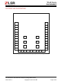
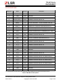
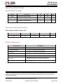
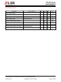
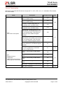
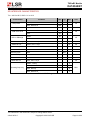
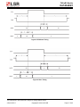
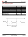
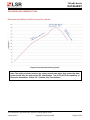
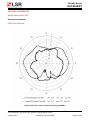
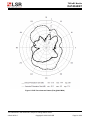
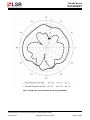
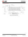
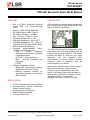
TiWi-uB1 Module DATASHEET TiWi-uB1 Bluetooth Smart (BLE) Module FEATURES DESCRIPTION Built in CC2541 single-chip Bluetooth Smart (BLE 4.0) System-On-Chip (SOC). Memory: 256kB FLASH, 8kB RAM RF Output Power: 0 dBm (Class 3) RF Receive Sensitivity: -94 dBm Size: 11.6mm x 17.9 mm x 2.3 mm Operating Voltage: 2.0V to 3.6V Operating Temperature: -40 to +85o C Worldwide Acceptance: FCC (USA), IC (Canada), ETSI (Europe), Giteki (Japan) REACH and RoHS compliant Complete power-optimized stack, including Controller and Host o GAP – Central, Peripheral, Observer, or Broadcaster (Including Combination Roles) o ATT/GATT – Client and Server o SMP – AES-128 Encryption and Decryption o L2CAP Multiple Configuration Options o Single-Chip Configuration, Allowing Applications to Run on CC2541 o Network Processor Interface for Applications Running on an External Microcontroller LSR would like to announce a low-cost and lowpower consumption module which has all of the BluetoothSmart functionalities. The TiWi-uB1 module fully supports the single mode Bluetooth Low Energy operation, and the output power can support class 3. The module provides the ability to either put your entire application into the integrated 8051 microcontroller, or use the module in Network Processor mode in conjunction with the microcontroller of your choice. Need to get to market quickly? Not an expert in Bluetooth Low Energy? Need a custom antenna? Do you need help with your host board? LSR Design Services will be happy to develop custom hardware or software, or help integrate the design. Contact us at [email protected] or call us at 262-375-4400. APPLICATIONS 2.4 GHz Bluetooth Low Energy Systems Human-Interface Devices (Keyboard, Mouse, Remote Control) Sports and Leisure Equipment Mobile Phone Accessories Consumer Electronics The information in this document is subject to change without notice. 330-0132-R1.5 Copyright © 2013-2015 LSR Page 1 of 42 TiWi-uB1 Module DATASHEET ORDERING INFORMATION Order Number Description 450-0103C TiWi-uB1 Module, PCB Trace Antenna (Cut Tape) 450-0103R TiWi-uB1 Module, PCB Trace Antenna (Tape & Reel) 450-0106C TiWi-uB1 Module, External Antenna Port (Cut Tape) 450-0106R TiWi-uB1 Module, External Antenna Port (Tape & Reel) 450-0120 TiWi-uB1 EM Board, PCB Trace Antenna Table 1 Orderable Model Numbers MODULE ACCESSORIES Order Number Description 001-0001 2.4 GHz Dipole Antenna with Reverse Polarity SMA Connector 080-0001 U.FL to Reverse Polarity SMA Bulkhead Cable 105mm Table 2 Module Accessories The information in this document is subject to change without notice. 330-0132-R1.5 Copyright © 2013-2015 LSR Page 2 of 42 TiWi-uB1 Module DATASHEET BLOCK DIAGRAM Off Module Antenna (optional) VCC /Reset 2 PCB Trace Antenna (optional) 19 CC2541 Bluetooth Low Energy (BLE) System-on-Chip (SOC) 32 MHz Crystal 2 Debug/IO I/O 32 kHz Crystal (optional) or I/O TiWi-uB1 Module Figure 1 TiWi-uB1 Module Block Diagram The information in this document is subject to change without notice. 330-0132-R1.5 Copyright © 2013-2015 LSR Page 3 of 42 TiWi-uB1 Module DATASHEET TABLE OF CONTENTS FEATURES .......................................................................................................................... 1 APPLICATIONS ................................................................................................................... 1 DESCRIPTION ..................................................................................................................... 1 ORDERING INFORMATION ................................................................................................ 2 MODULE ACCESSORIES ................................................................................................... 2 BLOCK DIAGRAM ............................................................................................................... 3 FOOTPRINT AND PIN DEFINITIONS.................................................................................. 6 PIN DESCRIPTIONS ............................................................................................................ 7 ELECTRICAL SPECIFICATIONS ........................................................................................ 8 Absolute Maximum Ratings ....................................................................................................................... 8 Recommended Operating Conditions ...................................................................................................... 8 General Characteristics .............................................................................................................................. 8 General Specifications ............................................................................................................................... 9 DC Characteristics .................................................................................................................................... 10 Current Consumption ............................................................................................................................... 11 CURRENT CONSUMPTION WITH DC to DC Converter ......................................................................... 12 RF Characteristics .................................................................................................................................... 13 SLOW CLOCK (32 KHZ) SOURCE REQUIREMENTS ..................................................... 14 32.768-kHz EXTERNAL CRYSTAL OSCILLATOR................................................................................... 14 32-kHz INTERNAL RC OSCILLATOR ....................................................................................................... 15 SPI INTERFACE CHARACTERISTICS ............................................................................. 16 DEBUG INTERFACE CHARACTERISTICS ...................................................................... 18 SOLDERING RECOMMENDATIONS ................................................................................ 20 Recommended Reflow Profile for Lead Free Solder ............................................................................. 20 CLEANING ......................................................................................................................... 21 OPTICAL INSPECTION ..................................................................................................... 21 REWORK ........................................................................................................................... 21 SHIPPING, HANDLING, AND STORAGE ......................................................................... 21 The information in this document is subject to change without notice. 330-0132-R1.5 Copyright © 2013-2015 LSR Page 4 of 42 TiWi-uB1 Module DATASHEET Shipping ..................................................................................................................................................... 21 Handling ..................................................................................................................................................... 21 Moisture Sensitivity Level (MSL) ............................................................................................................. 21 Storage ....................................................................................................................................................... 21 Repeating Reflow Soldering .................................................................................................................... 22 AGENCY CERTIFICATIONS ............................................................................................. 23 AGENCY STATEMENTS ................................................................................................... 23 Federal Communication Commission Interference Statement ............................................................ 23 Industry Canada Statements.................................................................................................................... 24 OEM RESPONSIBILITIES TO COMPLY WITH FCC AND INDUSTRY CANADA REGULATIONS ....................................................................................................... 25 OEM LABELING REQUIREMENTS FOR END-PRODUCT .............................................. 26 OEM END PRODUCT USER MANUAL STATEMENTS.................................................... 27 EUROPE ............................................................................................................................ 28 CE Notice ................................................................................................................................................... 28 Declaration of Conformity (DOC) ............................................................................................................ 28 BLUETOOTH CERTIFICATION ......................................................................................... 28 ANTENNA INFORMATION ................................................................................................ 29 Dipole Antenna 001-0001.......................................................................................................................... 29 PCB Trace Antenna ................................................................................................................................... 29 MECHANICAL DATA......................................................................................................... 38 PCB FOOTPRINT .............................................................................................................. 39 Tape & Reel Dimensions .......................................................................................................................... 40 DEVICE MARKINGS .......................................................................................................... 41 Rev 1 Devices ............................................................................................................................................ 41 Rev 2 Devices ............................................................................................................................................ 41 CONTACTING LSR............................................................................................................ 42 The information in this document is subject to change without notice. 330-0132-R1.5 Copyright © 2013-2015 LSR Page 5 of 42 TiWi-uB1 Module DATASHEET FOOTPRINT AND PIN DEFINITIONS 1 33 2 32 3 31 4 30 5 29 6 28 7 34 37 27 8 26 9 35 38 25 10 24 11 36 39 23 12 22 13 14 15 16 17 18 19 20 21 Figure 2 TiWi-uB1 Module Footprint (Viewed From Top) The information in this document is subject to change without notice. 330-0132-R1.5 Copyright © 2013-2015 LSR Page 6 of 42 TiWi-uB1 Module DATASHEET PIN DESCRIPTIONS Module Pin Name I/O Type Description 1 RF OUT RF 2 GND GND GROUND 3 GND GND GROUND 4 OSC32K_Q1/P2_4 AI/DIO GENERAL PURPOSE DIGITAL I/O 5 OSC32K_Q2/P2_3 AI/DIO 32KHZ GENERAL PURPOSE DIGITAL I/O 6 /RESET DI ACTIVE LOW RESET. CC2541 INTERNAL PULL-UP 7 DC/P2_2 DI/DIO DEBUG CLOCK, GENERAL PURPOSE DIGITAL I/O 8 DD/P2_1 DIO 9 NC - NO CONNECT (DO NOT CONNECT) 10 NC - NO CONNECT (DO NOT CONNECT) 11 AVCC PI ANALOG POWER SUPPLY TO MODULE (2.0V – 3.6V) 12 DVCC PI DIGITAL POWER TO SUPPLY MODULE (2.0V – 3.6V) 13 P2_0 DIO GENERAL PURPOSE DIGITAL I/O 14 SCL DIO I2C CLOCK, GENERAL PURPOSE DIGITAL I/O 15 SDA DIO I2C DATA, GENERAL PURPOSE DIGITAL I/O 16 P1_7 DIO GENERAL PURPOSE DIGITAL I/O 17 P1_6 DIO GENERAL PURPOSE DIGITAL I/O 18 P1_5 DIO GENERAL PURPOSE DIGITAL I/O 19 P1_4 DIO GENERAL PURPOSE DIGITAL I/O 20 P1_3 DIO GENERAL PURPOSE DIGITAL I/O 21 P1_2 DIO GENERAL PURPOSE DIGITAL I/O 22 GND GND GROUND 23 P1_1 DIO GENERAL PURPOSE DIGITAL I/O 24 P1_0 DIO GENERAL PURPOSE DIGITAL I/O 25 P0_7 DIO GENERAL PURPOSE DIGITAL I/O, ANALOG INPUT 26 P0_6 DIO GENERAL PURPOSE DIGITAL I/O, ANALOG INPUT 27 P0_5 DIO GENERAL PURPOSE DIGITAL I/O, ANALOG INPUT 28 P0_4 DIO GENERAL PURPOSE DIGITAL I/O, ANALOG INPUT 29 P0_3 DIO GENERAL PURPOSE DIGITAL I/O, ANALOG INPUT 30 P0_2 DIO GENERAL PURPOSE DIGITAL I/O, ANALOG INPUT 31 P0_1 DIO GENERAL PURPOSE DIGITAL I/O, ANALOG INPUT 32 P0_0 DIO GENERAL PURPOSE DIGITAL I/O, ANALOG INPUT 33 GND GND GROUND 34-39 GND GND GROUND AND THERMAL RELIEF PADS ANTENNA, 50 OHMS DEBUG DATA, GENERAL PURPOSE DIGITAL I/O PI = Power Input GND = Ground DI = Digital Input DO = Digital Output DIO = Digital Input/Output AI = Analog Input RF = Bi-directional RF Port Note: See the Texas Instruments CC2541 datasheet and user guide for further details on the I/O. Table 3 TiWi-uB1 Pin Descriptions The information in this document is subject to change without notice. 330-0132-R1.5 Copyright © 2013-2015 LSR Page 7 of 42 TiWi-uB1 Module DATASHEET ELECTRICAL SPECIFICATIONS Absolute Maximum Ratings Symbol Description Min Max Unit DVCC Digital Input Supply Voltage -0.3 3.9 V AVCC Analog Input Supply Voltage -0.3 3.9 V Voltage on any digital pin -0.3 VDD + 0.3 ≤ 3.9 V VDIO Table 4 Absolute Maximum Ratings 1 Recommended Operating Conditions Test conditions: Ambient Temp = 25°C Symbol VCC Min Typ 2.0 3.3 Table 5 Recommended Operating Conditions Max Unit 3.6 V General Characteristics Characteristic Description Model Name TiWi-uB1 Product Description Bluetooth Low Energy Wireless Module Dimension 11.63 mm x 17.86 mm x 2.4 mm (W*L*T) Operating temperature -40°C to 85°C Storage temperature -40°C to 85°C Humidity Operating Humidity 10% to 95% Non-Condensing Storage Humidity 5% to 95% Non-Condensing Weight 0.18 g +/- 0.01g Table 6 General Characteristics 1 Under no circumstances should exceeding the ratings specified in the Absolute Maximum Ratings section be allowed. Stressing the module beyond these limits may result permanent damage to the module that is not covered by the warranty. The information in this document is subject to change without notice. 330-0132-R1.5 Copyright © 2013-2015 LSR Page 8 of 42 TiWi-uB1 Module DATASHEET General Specifications Measured on LSR TiWi-uB1 EM reference design with TA = 25°C and VDD = 3 V Parameter Test Conditions Min Typ Max Unit WAKE-UP AND TIMING Digital regulator on, 16-MHz RCOSC and 32-MHz crystal oscillator off. Start-up of 16-MHz RCOSC 4 µS Power mode 1 → Active 120 µS Power mode 2 or 3 → Active Digital regulator off, 16-MHz RCOSC and 32-MHz crystal oscillator off. Start-up of regulator and 16MHz RCOSC Crystal ESR = 16 Ω. Initially running on 16MHz RCOSC, with 32-MHz XOSC OFF 500 µS With 32-MHz XOSC initially on 180 µS Proprietary auto mode 130 BLE mode 150 Active → TX or RX RX/TX turnaround Data rate and modulation format µS 2 Mbps, GFSK, 500-kHz deviation 2 Mbps, GFSK, 320-kHz deviation 1 Mbps, GFSK, 250-kHz deviation 1 Mbps, GFSK, 160-kHz deviation 500 kbps, MSK (Proprietary RF Only) 250 kbps, GFSK, 160-kHz deviation 250 kbps, MSK (Proprietary RF Only) Table 7 Bluetooth General Specifications The information in this document is subject to change without notice. 330-0132-R1.5 Copyright © 2013-2015 LSR Page 9 of 42 TiWi-uB1 Module DATASHEET DC Characteristics Parameter Test Conditions Min Typ Logic-0 input voltage Logic-1 input voltage Max Unit 0.5 V 2.4 V Logic-0 input current Input equals 0 V -50 50 nA Logic-1 input current Input equals VDD -50 50 nA I/O-pin pullup/pulldown resistors kΩ 20 Logic-0 output voltage, 4- mA pins Output load 4 mA Logic-1 output voltage, 4-mA pins Output load 4 mA Logic-0 output voltage, 20- mA pins Output load 20 mA Logic-1 output voltage, 20-mA pins Output load 20 mA 0.5 2.5 V 0.5 2.5 V V V Table 8 Bluetooth General DC Characteristics The information in this document is subject to change without notice. 330-0132-R1.5 Copyright © 2013-2015 LSR Page 10 of 42 TiWi-uB1 Module DATASHEET Current Consumption Measured on LSR TiWi-uB1 EM reference design with TA = 25°C, VDD = 3.3 V, fc = 2440 MHz. LEDs disabled, DC to DC disabled. Mode Description Icore Core current consumption Iperi Peripheral current consumption *Adds to core current Icore for each peripheral unit activated Average Current RX mode, standard mode, no peripherals active, low MCU activity 25.7 RX mode, high-gain mode, no peripherals active, low MCU activity 28.1 TX mode, –23 dBm output power, no peripherals active, low MCU activity 20.2 TX mode, 0 dBm output power, no peripherals active, low MCU activity 21.1 Power mode 1. Digital regulator on; 16MHz RCOSC and 32-MHz crystal oscillator off; 32.768-kHz XOSC, POR, BOD and sleep timer active; RAM and register retention 270 Power mode 2. Digital regulator off; 16MHz RCOSC and 32-MHz crystal oscillator off; 32.768-kHz XOSC, POR, and sleep timer active; RAM and register retention 1 Unit mA µA Power mode 3. Digital regulator off; no clocks; POR active; 0.5 RAM and register retention 0.5 Low MCU activity: 32-MHz XOSC running. No radio or peripherals. Limited flash access, no RAM access. 6.7 Timer 1. Timer running, 32-MHz XOSC used 90 Timer 2. Timer running, 32-MHz XOSC used 90 Timer 3. Timer running, 32-MHz XOSC used 60 Timer 4. Timer running, 32-MHz XOSC used 70 Sleep timer, including 32.753-kHz RCOSC 0.6 ADC, when converting 1.2 mA µA mA Table 9 Bluetooth General DC Characteristics The information in this document is subject to change without notice. 330-0132-R1.5 Copyright © 2013-2015 LSR Page 11 of 42 TiWi-uB1 Module DATASHEET CURRENT CONSUMPTION WITH DC to DC Converter Measured on LSR TiWi-uB1 EM reference design with TA = 25°C, VDD = 3.3 V, fc = 2440 MHz. LEDs disabled, DC to DC Enabled 1 Mbsp, GFSK, 250-kHz deviation, Bluetooth™ low energy Mode, 1% BER. Mode Current consumption Description Average Current RX mode, standard mode, no peripherals active, low MCU activity 15.7 RX mode, high-gain mode, no peripherals active, low MCU activity 17.4 TX mode, –23 dBm output power, no peripherals active, low MCU activity 12.0 TX mode, 0 dBm output power, no peripherals active, low MCU activity 12.6 Unit mA Table 10 Bluetooth Power Consumption The information in this document is subject to change without notice. 330-0132-R1.5 Copyright © 2013-2015 LSR Page 12 of 42 TiWi-uB1 Module DATASHEET RF Characteristics Measured on LSR TiWi-uB1 EM reference design with TA = 25°C, VDD = 3.3 V, fc = 2440 MHz. LEDs disabled, DC to DC disabled, measured at RF connector. Parameter Test Conditions Min Typ Max Unit TRANSMIT SECTION Output Power Measured on LSR TiWi-uB1 450-0106 EM reference design at RF connector using maximum recommended output power setting 0 Measured on LSR TiWi-uB1 450-0106 EM reference design at RF connector using minimum recommended output power setting -23 dBm Spurious emission conducted measurement f < 1 GHz -52 dBm f > 1 GHz -48 dBm RF frequency range Programmable in 1-MHz steps 2379 2496 MHz RECEIVE SECTION 1 Mbps, GFSK, 250-kHz Deviation, Bluetooth low energy Mode, 0.1% BER, High Gain Mode -94 dBm 1 Mbps, GFSK, 250-kHz Deviation, Bluetooth low energy Mode, 0.1% BER, Standard Gain Mode -88 dBm Receiver sensitivity Saturation(2) BER < 0.1% 5 dBm Co-channel rejection (2) Wanted signal –67 dBm -6 dB Frequency error tolerance Including both initial tolerance and drift. Sensitivity better than -67dBm, 250 byte payload. BER 0.1% Intermodulation (1) Minimum interferer level Table 11 Bluetooth RF Characteristics -250 250 -36 KHz dBm 1. Results based on standard-gain mode. The information in this document is subject to change without notice. 330-0132-R1.5 Copyright © 2013-2015 LSR Page 13 of 42 TiWi-uB1 Module DATASHEET SLOW CLOCK (32 KHZ) SOURCE REQUIREMENTS Two 32-kHz oscillators are available in the device as clock sources for the 32-kHz clock: • 32-kHz XOSC – External Crystal Oscillator • 32-kHz RCOSC – Internal RC Oscillator By default, after a reset, the 32-kHz RCOSC is enabled and selected as the 32-kHz clock source. The RCOSC consumes less power, but is less accurate compared to the 32-kHz XOSC. The chosen 32-kHz clock source drives the Sleep Timer, generates the tick for the Watchdog Timer, and is used as a strobe in Timer 2 to calculate the Sleep Timer sleep time. The crystal is required for accurate sleep timing, so it is only needed to for the module be BLE certified when using low power modes. 32.768-kHz EXTERNAL CRYSTAL OSCILLATOR Characteristic Condition Min Crystal frequency Typ Max 32768 Crystal frequency accuracy requirement -40 Unit Hz 40 ppm ESR Equivalent series Resistance 40 130 kΩ C0 Crystal shunt Capacitance 0.9 2 pF CL Crystal load capacitance 12 16 pF Start-up time 0.4 mS Table 12 32 kHz External Clock Requirements The information in this document is subject to change without notice. 330-0132-R1.5 Copyright © 2013-2015 LSR Page 14 of 42 TiWi-uB1 Module DATASHEET 32-kHz INTERNAL RC OSCILLATOR Characteristic Condition Min Calibrated frequency (1) Typ Max 32768 Frequency accuracy after calibration -40 Temperature coefficient (2) Unit Hz 40 ppm ±0.2 % Supply-voltage coefficient 3 %/V Calibration time (3) 2 mS Table 13 32 kHz Internal Clock Requirements 1) The calibrated 32-kHz RC oscillator frequency is 32-MHz divided by 977. 2) Frequency drift when temperature changes after calibration. 3) When the 32-kHz RC oscillator is enabled, it is calibrated when a switch from the 16-MHz RC oscillator to the 32-MHz crystal oscillator is performed while SLEEPCMD.OSC32K_CALDIS is set to 0. The information in this document is subject to change without notice. 330-0132-R1.5 Copyright © 2013-2015 LSR Page 15 of 42 TiWi-uB1 Module DATASHEET SPI INTERFACE CHARACTERISTICS TA = –40°C to 85°C, VDD = 2 V to 3.6 V Characteristic t1 SCK period SCK duty cycle t2 SSN low to SCK t3 SCK to SSN high Condition Min Master, RX and TX 250 Slave, RX and TX 250 Master Typ Max Unit nS 50% Master 63 Slave 63 Master 63 Slave 63 nS nS T4 SCK to SSN high Master, load = 10 pF 7 nS t5 MOSI late out Master, load = 10 pF 10 nS t6 MISO setup Master nS t7 MISO hold Master nS SCK duty cycle Slave t10 MOSI setup Slave nS t11 MOSI hold Slave nS t9 MISO late out Slave, load = 10 pF nS Operating frequency 50% Master, TX only 8 Master, RX and TX 4 Slave, RX only 8 Slave, RX and TX 4 MHz Table 14 SPI Timing The information in this document is subject to change without notice. 330-0132-R1.5 Copyright © 2013-2015 LSR Page 16 of 42 TiWi-uB1 Module DATASHEET Figure 3 SPI Master Timing Figure 4 Slave Timing The information in this document is subject to change without notice. 330-0132-R1.5 Copyright © 2013-2015 LSR Page 17 of 42 TiWi-uB1 Module DATASHEET DEBUG INTERFACE CHARACTERISTICS TA = –40°C to 85°C, VDD = 2 V to 3.6 V Characteristic Condition Min fclk_ dbg Debug clock frequency (see Figure 5) Typ Max Unit 12 MHz t1 Allowed high pulse on clock (see Figure 5) 35 ns t2 Allowed low pulse on clock (see Figure 5) 35 ns t 167 ns t4 Falling edge on clock to EXT_RESET_N high (see Figure 7) 83 ns t6EXT_RESET_N high to first debug command (see Figure 7) 83 ns t6 Debug data setup (see Figure 6) 2 ns t7 Debug data hold (see Figure 6) 4 ns 3 EXT_RESET_N low to first falling edge on debug clock (see Figure 7) t8 Clock-to-data delay (see Figure 6) Load = 10 pF ns Table 15 Debug Interface Timing Figure 5 Slave Timing The information in this document is subject to change without notice. 330-0132-R1.5 Copyright © 2013-2015 LSR Page 18 of 42 TiWi-uB1 Module DATASHEET Figure 6 Slave Timing Figure 7 Slave Timing The information in this document is subject to change without notice. 330-0132-R1.5 Copyright © 2013-2015 LSR Page 19 of 42 TiWi-uB1 Module DATASHEET SOLDERING RECOMMENDATIONS Recommended Reflow Profile for Lead Free Solder Figure 8 Recommended Soldering Profile Note: The quality of solder joints on the surface mount pads where they contact the host board should meet the appropriate IPC Specification. See IPC-A-610-D Acceptability of Electronic Assemblies, section 8.2.1 “Bottom Only Terminations.” The information in this document is subject to change without notice. 330-0132-R1.5 Copyright © 2013-2015 LSR Page 20 of 42 TiWi-uB1 Module DATASHEET CLEANING SHIPPING, HANDLING, AND STORAGE In general, cleaning the populated modules is strongly discouraged. Residuals under the module cannot be easily removed with any cleaning process. Shipping Cleaning with water can lead to capillary effects where water is absorbed into the gap between the host board and the module. The combination of soldering flux residuals and encapsulated water could lead to short circuits between neighboring pads. Water could also damage any stickers or labels. Cleaning with alcohol or a similar organic solvent will likely flood soldering flux residuals into the RF shield, which is not accessible for post-washing inspection. The solvent could also damage any stickers or labels. Ultrasonic cleaning could damage the module permanently. OPTICAL INSPECTION After soldering the Module to the host board, consider optical inspection to check the following: Proper alignment and centering of the module over the pads. Proper solder joints on all pads. Excessive solder or contacts to neighboring pads, or vias. REWORK The module can be unsoldered from the host board if the Moisture Sensitivity Level (MSL) requirements are met as described in this datasheet. Bulk orders of the TiWi-uB1 modules are delivered in reels of 1,000. Handling The TiWi-uB1 modules contain a highly sensitive electronic circuitry. Handling without proper ESD protection may damage the module permanently. Moisture Sensitivity Level (MSL) Per J-STD-020, devices rated as MSL 4 and not stored in a sealed bag with desiccant pack should be baked prior to use. Devices are packaged in a Moisture Barrier Bag with a desiccant pack and Humidity Indicator Card (HIC). Devices that will be subjected to reflow should reference the HIC and J-STD-033 to determine if baking is required. If baking is required, refer to J-STD-033 for bake procedure. Storage Per J-STD-033, the shelf life of devices in a Moisture Barrier Bag is 12 months at <40ºC and <90% room humidity (RH). Do not store in salty air or in an environment with a high concentration of corrosive gas, such as Cl2, H2S, NH3, SO2, or NOX. Do not store in direct sunlight. The product should not be subject to excessive mechanical shock. Never attempt a rework on the module itself, e.g. replacing individual components. Such actions will terminate warranty coverage. The information in this document is subject to change without notice. 330-0132-R1.5 Copyright © 2013-2015 LSR Page 21 of 42 TiWi-uB1 Module DATASHEET Repeating Reflow Soldering Only a single reflow soldering process is encouraged for host boards. The information in this document is subject to change without notice. 330-0132-R1.5 Copyright © 2013-2015 LSR Page 22 of 42 TiWi-uB1 Module DATASHEET AGENCY CERTIFICATIONS FCC ID: TFB-BT2, 15.247 IC ID: 5969A-BT2, RSS 210 CE: Compliant to standards EN 60950-1, EN 300 328, and EN 301 489 Giteki: 209-J00156 AGENCY STATEMENTS Federal Communication Commission Interference Statement This equipment has been tested and found to comply with the limits for a Class B digital device, pursuant to Part 15 of the FCC Rules. These limits are designed to provide reasonable protection against harmful interference in a residential installation. This equipment generates uses and can radiate radio frequency energy and, if not installed and used in accordance with the instructions, may cause harmful interference to radio communications. However, there is no guarantee that interference will not occur in a particular installation. If this equipment does cause harmful interference to radio or television reception, which can be determined by turning the equipment off and on, the user is encouraged to try to correct the interference by one of the following measures: Reorient or relocate the receiving antenna. Increase the separation between the equipment and receiver. Connect the equipment into an outlet on a circuit different from that to which the receiver is connected. Consult the dealer or an experienced radio/TV technician for help. This device complies with Part 15 of the FCC Rules. Operation is subject to the following two conditions: (1) This device may not cause harmful interference, and (2) this device must accept any interference received, including interference that may cause undesired operation. This portable transmitter with its antenna complies with FCC/IC RF exposure limits for general population / uncontrolled exposure. FCC CAUTION: Any changes or modifications not expressly approved by the party responsible for compliance could void the user's authority to operate this equipment. The information in this document is subject to change without notice. 330-0132-R1.5 Copyright © 2013-2015 LSR Page 23 of 42 TiWi-uB1 Module DATASHEET Industry Canada Statements This device complies with Industry Canada License-exempt RSS standard(s). Operation is subject to the following two conditions: (1) this device may not cause interference, and (2) this device must accept any interference, including interference that may cause undesired operation of the device. To reduce potential radio interference to other users, the antenna type and its gain should be so chosen that the equivalent isotropically radiated power (e.i.r.p.) is not more than that permitted for successful communication. This device has been designed to operate with the antenna(s) listed below, and having a maximum gain of -4.2 dBi (PCB Trace) and 2.0dBi (LSR 2.4 GHz Dipole). Antennas not included in this list or having a gain greater than -4.2 dBi and 2.0 dBi are strictly prohibited for use with this device. The required antenna impedance is 50 ohms. List of all Antennas Acceptable for use with the Transmitter 1) On module PCB trace antenna. 2) LSR 001-0001 center-fed 2.4 GHz dipole antenna and LSR 080-0001 U.FL to Reverse Polarity SMA connector cable. Cet appareil est conforme aux normes d'Industrie Canada exempts de licence RSS (s). L'opération est soumise aux deux conditions suivantes: (1) cet appareil ne peut pas provoquer d'interférences et (2) cet appareil doit accepter toute interférence, y compris les interférences qui peuvent causer un mauvais fonctionnement de l'appareil. Pour réduire le risque d'interférence aux autres utilisateurs, le type d'antenne et son gain doiventêtre choisis de manière que la puissance isotrope rayonnée équivalente (PIRE) ne dépasse pascelle permise pour une communication réussie. Cet appareil a été conçu pour fonctionner avec l'antenne (s) ci-dessous, et ayant un gain maximum de -4,2 dBi (PCB Trace) et 2,0 dBi (LSR 2.4 GHz Dipole). Antennes pas inclus dans cette liste ou présentant un gain supérieur à -4,2 dBi et 2,0 dBi sont strictement interdits pour une utilisation avec cet appareil. L'impédance d'antenne requise est de 50 ohms. Liste de toutes les antennes acceptables pour une utilisation avec l'émetteur 1) Le module d'antenne PCB trace. 2) LSR 001-0001 centre-fed 2,4 GHz antenne dipôle et LSR 080-0001 U.FL pour inverser câble connecteur SMA à polarité. The information in this document is subject to change without notice. 330-0132-R1.5 Copyright © 2013-2015 LSR Page 24 of 42 TiWi-uB1 Module DATASHEET OEM RESPONSIBILITIES TO COMPLY WITH FCC AND INDUSTRY CANADA REGULATIONS The TiWi-uB1 Module has been certified for integration into products only by OEM integrators under the following conditions: The antennas for this transmitter must not be co-located with any other transmitters except in accordance with FCC and Industry Canada multi-transmitter procedures. Co-location means having a separation distance of less than 20 cm between transmitting antennas. As long as the two conditions above are met, further transmitter testing will not be required. However, the OEM integrator is still responsible for testing their end-product for any additional compliance requirements required with this module installed (for example, digital device emissions, PC peripheral requirements, etc.). IMPORTANT NOTE: In the event that these conditions cannot be met (for certain configurations or co-location with another transmitter), then the FCC and Industry Canada authorizations are no longer considered valid and the FCC ID and IC Certification Number cannot be used on the final product. In these circumstances, the OEM integrator will be responsible for re-evaluating the end product (including the transmitter) and obtaining a separate FCC and Industry Canada authorization. Le module de TiWi-uB1 a été certifié pour l'intégration dans des produits uniquement par des intégrateurs OEM dans les conditions suivantes: Les antennes pour ce transmetteur ne doit pas être co-localisés avec les autres émetteurs sauf en conformité avec la FCC et Industrie Canada multi-émetteur procédures. Co-localisation des moyens ayant une distance de séparation inférieure à 20 cm entre les antennes d'émission. Tant que les deux conditions précitées sont réunies, les tests de transmetteurs supplémentaires ne seront pas tenus. Toutefois, l'intégrateur OEM est toujours responsable de tester leur produit final pour toutes les exigences de conformité supplémentaires requis avec ce module installé (par exemple, les émissions appareil numérique, les exigences de périphériques PC, etc.) NOTE IMPORTANTE: Dans le cas où ces conditions ne peuvent être satisfaites (pour certaines configurations ou de co-implantation avec un autre émetteur), puis la FCC et Industrie autorisations Canada ne sont plus considérés comme valides et l'ID de la FCC et IC numéro de certification ne peut pas être utilisé sur la produit final. Dans ces circonstances, l'intégrateur OEM sera chargé de réévaluer le produit final (y compris l'émetteur) et l'obtention d'un distincte de la FCC et Industrie Canada l'autorisation. The information in this document is subject to change without notice. 330-0132-R1.5 Copyright © 2013-2015 LSR Page 25 of 42 TiWi-uB1 Module DATASHEET OEM LABELING REQUIREMENTS FOR END-PRODUCT The TiWi-uB1 module is labeled with its own FCC ID and IC Certification Number. The FCC ID and IC certification numbers are not visible when the module is installed inside another device, as such the end device into which the module is installed must display a label referring to the enclosed module. The final end product must be labeled in a visible area with the following: “Contains Transmitter Module FCC ID: TFB-BT2” “Contains Transmitter Module IC: 5969A-BT2” or “Contains FCC ID: TFB-BT2” “Contains IC: 5969A-BT2” The OEM of the TiWi-uB1 Module must only use the approved antenna(s) listed above, which have been certified with this module. Le module de TiWi-uB1 est étiqueté avec son propre ID de la FCC et IC numéro de certification. L'ID de la FCC et IC numéros de certification ne sont pas visibles lorsque le module est installé à l'intérieur d'un autre appareil, comme par exemple le terminal dans lequel le module est installé doit afficher une etiquette faisant référence au module ci-joint. Le produit final doit être étiqueté dans un endroit visible par le suivant: “Contient Module émetteur FCC ID: TFB-BT2" “Contient Module émetteur IC: 5969A-BT2" ou “Contient FCC ID: TFB-BT2" “Contient IC: 5969A-BT2" Les OEM du module TiWi-uB1 ne doit utiliser l'antenne approuvée (s) ci-dessus, qui ont été certifiés avec ce module. The information in this document is subject to change without notice. 330-0132-R1.5 Copyright © 2013-2015 LSR Page 26 of 42 TiWi-uB1 Module DATASHEET OEM END PRODUCT USER MANUAL STATEMENTS The OEM integrator should not provide information to the end user regarding how to install or remove this RF module or change RF related parameters in the user manual of the end product. Other user manual statements may apply. L'intégrateur OEM ne devraient pas fournir des informations à l'utilisateur final sur la façon d'installer ou de supprimer ce module RF ou modifier les paramètres liés RF dans le manuel utilisateur du produit final. Autres déclarations manuel de l'utilisateur peuvent s'appliquer. The information in this document is subject to change without notice. 330-0132-R1.5 Copyright © 2013-2015 LSR Page 27 of 42 TiWi-uB1 Module DATASHEET EUROPE CE Notice This device has been tested and certified for use in the European Union. See the Declaration of Conformity (DOC) for specifics. If this device is used in a product, the OEM has responsibility to verify compliance of the final product to the EU standards. A Declaration of Conformity must be issued and kept on file as described in the Radio and Telecommunications Terminal Equipment (R&TTE) Directive. The ‘CE’ mark must be placed on the OEM product per the labeling requirements of the Directive. Declaration of Conformity (DOC) The DOC can be downloaded from the LSR Wiki. BLUETOOTH CERTIFICATION The TiWi-uB1 module has been certified as a Controller Subsystem and has a QDID of B021230. The information in this document is subject to change without notice. 330-0132-R1.5 Copyright © 2013-2015 LSR Page 28 of 42 TiWi-uB1 Module DATASHEET ANTENNA INFORMATION Dipole Antenna 001-0001 See antenna datasheet. PCB Trace Antenna Figure 9 PCB Trace Antenna Pattern (Vertical @ 2405 MHz) The information in this document is subject to change without notice. 330-0132-R1.5 Copyright © 2013-2015 LSR Page 29 of 42 TiWi-uB1 Module DATASHEET Figure 10 PCB Trace Antenna Pattern (Horizontal @ 2405 MHz) The information in this document is subject to change without notice. 330-0132-R1.5 Copyright © 2013-2015 LSR Page 30 of 42 TiWi-uB1 Module DATASHEET Figure 11 PCB Trace Antenna Pattern (Flat @ 2405 MHz) The information in this document is subject to change without notice. 330-0132-R1.5 Copyright © 2013-2015 LSR Page 31 of 42 TiWi-uB1 Module DATASHEET Figure 12 PCB Trace Antenna Pattern (Vertical @ 2440 MHz) The information in this document is subject to change without notice. 330-0132-R1.5 Copyright © 2013-2015 LSR Page 32 of 42 TiWi-uB1 Module DATASHEET Figure 13 PCB Trace Antenna Pattern (Horizontal @ 2440 MHz) The information in this document is subject to change without notice. 330-0132-R1.5 Copyright © 2013-2015 LSR Page 33 of 42 TiWi-uB1 Module DATASHEET Figure 14 PCB Trace Antenna Pattern (Flat @ 2440 MHz) The information in this document is subject to change without notice. 330-0132-R1.5 Copyright © 2013-2015 LSR Page 34 of 42 TiWi-uB1 Module DATASHEET Figure 15 PCB Trace Antenna Pattern (Vertical @ 2480 MHz) The information in this document is subject to change without notice. 330-0132-R1.5 Copyright © 2013-2015 LSR Page 35 of 42 TiWi-uB1 Module DATASHEET Figure 16 PCB Trace Antenna Pattern (Horizontal @ 2480 MHz) The information in this document is subject to change without notice. 330-0132-R1.5 Copyright © 2013-2015 LSR Page 36 of 42 TiWi-uB1 Module DATASHEET Figure 17 PCB Trace Antenna Pattern (Flat @ 2480 MHz) The information in this document is subject to change without notice. 330-0132-R1.5 Copyright © 2013-2015 LSR Page 37 of 42 TiWi-uB1 Module DATASHEET MECHANICAL DATA Figure 18 Module Mechanical Dimensions (Maximum Module Height = 2.3mm) The information in this document is subject to change without notice. 330-0132-R1.5 Copyright © 2013-2015 LSR Page 38 of 42 TiWi-uB1 Module DATASHEET PCB FOOTPRINT Figure 19 TiWi-uB1 Recommended PCB Footprint (Viewed from Top) The information in this document is subject to change without notice. 330-0132-R1.5 Copyright © 2013-2015 LSR Page 39 of 42 TiWi-uB1 Module DATASHEET Tape & Reel Dimensions Figure 20 Tape and Reel Specification The information in this document is subject to change without notice. 330-0132-R1.5 Copyright © 2013-2015 LSR Page 40 of 42 TiWi-uB1 Module DATASHEET DEVICE MARKINGS Rev 1 Devices LSR Model: TiWi-uB1 P/N: 450-0103-R1 FCC ID: TFB-BT2 IC: 5969A-BT2 20D1D0001 The shield on the 450-0103 / 450-0106 modules contains the following information: LSR Model: TiWi-uB1 Part Number and Revision: o Part Number: 450-0103 or 450-0106 o Revision: -RX (where X is the latest revision) FCC ID: TFB-BT2 IC: 5969A-BT2 Manufacturer Information Rev 2 Devices Updated the label to include Giteki EMC marking information. Updated the label to include a date code. Where RX = Revision X SSYYWWD = Date Code (YY=Year, WW=Week) XXXXX = Incremental Serial Number 2D Barcode Format is Data Matrix Standard The information in this document is subject to change without notice. 330-0132-R1.5 Copyright © 2013-2015 LSR Page 41 of 42 TiWi-uB1 Module DATASHEET CONTACTING LSR Headquarters LSR W66 N220 Commerce Court Cedarburg, WI 53012-2636 USA Tel: 1(262) 375-4400 Fax: 1(262) 375-4248 Website www.lsr.com Sales Contact [email protected] The information in this document is provided in connection with LS Research (hereafter referred to as “LSR”) products. No license, express or implied, by estoppel or otherwise, to any intellectual property right is granted by this document or in connection with the sale of LSR products. EXCEPT AS SET FORTH IN LSR’S TERMS AND CONDITIONS OF SALE LOCATED ON LSR’S WEB SITE, LSR ASSUMES NO LIABILITY WHATSOEVER AND DISCLAIMS ANY EXPRESS, IMPLIED OR STATUTORY WARRANTY RELATING TO ITS PRODUCTS INCLUDING, BUT NOT LIMITED TO, THE IMPLIED WARRANTY OF MERCHANTABILITY, FITNESS FOR A PARTICULAR PURPOSE, OR NON-INFRINGEMENT. IN NO EVENT SHALL LSR BE LIABLE FOR ANY DIRECT, INDIRECT, CONSEQUENTIAL, PUNITIVE, SPECIAL OR INCIDENTAL DAMAGES (INCLUDING, WITHOUT LIMITATION, DAMAGES FOR LOSS OF PROFITS, BUSINESS INTERRUPTION, OR LOSS OF INFORMATION) ARISING OUT OF THE USE OR INABILITY TO USE THIS DOCUMENT, EVEN IF LSR HAS BEEN ADVISED OF THE POSSIBILITY OF SUCH DAMAGES. LSR makes no representations or warranties with respect to the accuracy or completeness of the contents of this document and reserves the right to make changes to specifications and product descriptions at any time without notice. LSR does not make any commitment to update the information contained herein. Unless specifically provided otherwise, LSR products are not suitable for, and shall not be used in, automotive applications. LSR’s products are not intended, authorized, or warranted for use as components in applications intended to support or sustain life. The information in this document is subject to change without notice. 330-0132-R1.5 Copyright © 2013-2015 LSR Page 42 of 42