1
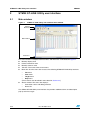
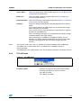
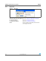
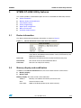
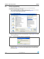
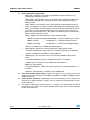
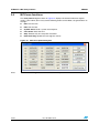
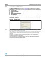
UM0892
User manual
STM32 ST-LINK Utility software description
Introduction
The STM32 ST-LINK Utility software facilitates fast in-system programming of the STM32
microcontroller families in development environments via the tools, ST-LINK and
ST-LINK/V2.
This is the STM32 ST-LINK Utility user manual, describing its software functions. When
working with the STM32 ST-LINK Utility, you are encouraged to download the ST-LINK
in-circuit debugger/programmer user manual (UM0627) or the ST-LINK/V2 in-circuit
debugger/programmer user manual (UM1075) for the STM8 and STM32 which provide
more information about the ST-LINK tools.
Table 1.
Applicable tools
Type
Development tools
October 2012
Part number
ST-LINK, ST-LINK/V2
Doc ID 16987 Rev 9
1/28
www.st.com
Contents
UM0892
Contents
1
2
3
4
Getting started . . . . . . . . . . . . . . . . . . . . . . . . . . . . . . . . . . . . . . . . . . . . . . 3
1.1
System requirements . . . . . . . . . . . . . . . . . . . . . . . . . . . . . . . . . . . . . . . . . 3
1.2
Hardware requirements . . . . . . . . . . . . . . . . . . . . . . . . . . . . . . . . . . . . . . . 3
1.3
Installing the STM32 ST-LINK Utility . . . . . . . . . . . . . . . . . . . . . . . . . . . . . 3
1.4
Uninstalling the STM32 ST-LINK Utility . . . . . . . . . . . . . . . . . . . . . . . . . . . 3
STM32 ST-LINK Utility user interface . . . . . . . . . . . . . . . . . . . . . . . . . . . 4
2.1
Main window . . . . . . . . . . . . . . . . . . . . . . . . . . . . . . . . . . . . . . . . . . . . . . . . 4
2.2
Menu bar . . . . . . . . . . . . . . . . . . . . . . . . . . . . . . . . . . . . . . . . . . . . . . . . . . 5
2/28
File menu . . . . . . . . . . . . . . . . . . . . . . . . . . . . . . . . . . . . . . . . . . . . . . . . . 5
2.2.2
View menu . . . . . . . . . . . . . . . . . . . . . . . . . . . . . . . . . . . . . . . . . . . . . . . . 5
2.2.3
Target menu . . . . . . . . . . . . . . . . . . . . . . . . . . . . . . . . . . . . . . . . . . . . . . . 6
2.2.4
ST-LINK menu . . . . . . . . . . . . . . . . . . . . . . . . . . . . . . . . . . . . . . . . . . . . . 7
2.2.5
Help menu . . . . . . . . . . . . . . . . . . . . . . . . . . . . . . . . . . . . . . . . . . . . . . . . 8
STM32 ST-LINK Utility features . . . . . . . . . . . . . . . . . . . . . . . . . . . . . . . . 9
3.1
Device information . . . . . . . . . . . . . . . . . . . . . . . . . . . . . . . . . . . . . . . . . . . 9
3.2
Memory display and modification . . . . . . . . . . . . . . . . . . . . . . . . . . . . . . . . 9
3.3
Flash memory erase . . . . . . . . . . . . . . . . . . . . . . . . . . . . . . . . . . . . . . . . 11
3.4
Device programming . . . . . . . . . . . . . . . . . . . . . . . . . . . . . . . . . . . . . . . . 12
3.5
Option bytes configuration . . . . . . . . . . . . . . . . . . . . . . . . . . . . . . . . . . . . 13
3.6
MCU core functions . . . . . . . . . . . . . . . . . . . . . . . . . . . . . . . . . . . . . . . . . 16
3.7
Automatic mode functions . . . . . . . . . . . . . . . . . . . . . . . . . . . . . . . . . . . . 17
STM32 ST-LINK Utility command line interface (CLI) . . . . . . . . . . . . . 18
4.1
5
2.2.1
Command line usage . . . . . . . . . . . . . . . . . . . . . . . . . . . . . . . . . . . . . . . . 18
4.1.1
Connection and memory manipulation commands . . . . . . . . . . . . . . . . 18
4.1.2
Core commands . . . . . . . . . . . . . . . . . . . . . . . . . . . . . . . . . . . . . . . . . . 19
4.1.3
Flash commands . . . . . . . . . . . . . . . . . . . . . . . . . . . . . . . . . . . . . . . . . . 20
4.1.4
Option byte commands . . . . . . . . . . . . . . . . . . . . . . . . . . . . . . . . . . . . . 21
4.1.5
ST-LINK_CLI return codes . . . . . . . . . . . . . . . . . . . . . . . . . . . . . . . . . . . 25
Revision history . . . . . . . . . . . . . . . . . . . . . . . . . . . . . . . . . . . . . . . . . . . 26
Doc ID 16987 Rev 9
UM0892
1
Getting started
Getting started
This section describes the requirements and procedures to install the STM32 ST-LINK Utility
software.
1.1
System requirements
The STM32 ST-LINK Utility PC configuration requires as a minimum:
●
PC with USB port and Intel® Pentium® processor running a 32-bit version of one of the
following Microsoft® operating systems:
1.2
–
Windows® XP
–
Windows 7
●
32 Mbytes of RAM
●
10 Mbytes of hard disk space available
Hardware requirements
The STM32 ST-LINK Utility is designed to work with:
●
STM32 F0, STM32 F1, STM32 F2, STM32 F3, STM32 F4, STM32 L1, and STM32W
series
●
ST-LINK or ST-LINK/V2 or ST-LINK/V2-ISOL in-circuit debugger/programmer probe
Note:
In this document, ST-LINK/V2 refer to ST-LINK/V2 and ST-LINK/V2-ISOL which are
functionally equivalent.
1.3
Installing the STM32 ST-LINK Utility
Follow these steps and the on-screen instructions to install the STM32 ST-LINK Utility.
1.4
1.
Download the compressed STM32 ST-LINK Utility software from the ST website.
2.
Extract the contents of the .zip file into a temporary directory.
3.
Double-click the extracted executable, setup.exe, to initiate the installation, and follow
the on-screen prompts to install the STM32 ST-LINK Utility in the development
environment. Documentation for the utility is located in the subdirectory \Docs where
the STM32 ST-LINK Utility is installed.
Uninstalling the STM32 ST-LINK Utility
Follow these steps to uninstall the STM32 ST-LINK Utility.
1.
Select Start | Settings | Control Panel.
2.
Double-click on Add or Remove Programs.
3.
Select STM32 ST-LINK Utility.
4.
Click on the Remove button.
Doc ID 16987 Rev 9
3/28
STM32 ST-LINK Utility user interface
UM0892
2
STM32 ST-LINK Utility user interface
2.1
Main window
Figure 1.
STM32 ST-LINK Utility user interface main window
Title bar
Menu bar
Main window
Status bar
The main window is composed of three zones and three bars as illustrated in Figure 1:
●
Memory display zone
●
Device information zone
●
Memory contents zone
●
Title bar: The name of the current menu
●
Menu bar: Use the menu bar to access the following STM32 ST-LINK Utility functions:
–
File menu
–
View menu
–
Target menu
–
Help menu
(These menus are described in more detail in Section 2.2)
●
Status window: The status bar displays:
–
Connection status and debug interface
–
Device ID
The STM32 ST-LINK Utility user interface also provides additional forms and descriptive
pop-up error messages.
4/28
Doc ID 16987 Rev 9
UM0892
2.2
STM32 ST-LINK Utility user interface
Menu bar
The Menu bar allows users to execute the STM32 ST-LINK Utility software features.
2.2.1
File menu
Figure 2.
2.2.2
File menu
Open file...
Opens a binary, Intel Hex or Motorola S-record.
Save file as…
Saves the content of the memory panel into a binary, Intel Hex or
Motorola S-record.
Close File
Closes the loaded file.
Compare two
files
Compares two binary, hex, or srec files. The difference is colored in
red in the file panel. If a file contains a section with an address range
that is unavailable in the other file, this section will be colored in
violet.
Exit
Closes the STM32 ST-LINK Utility program.
View menu
Figure 3.
Binary file
View menu
Displays the content of the loaded binary file.
Device memory Displays the content of the device memory.
Doc ID 16987 Rev 9
5/28
STM32 ST-LINK Utility user interface
2.2.3
Target menu
Figure 4.
6/28
UM0892
Target menu
Connect
Connects to the target device and displays the Device Type, Device ID
and Flash memory size in the device information zone.
Disconnect
Disconnects from the target device.
Erase Chip
Performs a Flash memory mass erase and then displays the Flash
memory content in the memory panel.
Erase Bank1
Erases bank 1 of the Flash memory. This menu is enabled only when
connected to an XL-density device.
Erase Bank2
Erases bank 2 of the Flash memory. This menu is enabled only when
connected to an XL-density device.
Erase Sectors…
Selects sector(s) to erase using the erase sectors dialog window (see
Section 3.3: Flash memory erase for more details).
Program…
Loads a binary, Intel Hex or Motorola S-record file into the device
memory (Flash or RAM). To do this, select a binary, Intel Hex or
Motorola S-record file, enter the start address (where to put the file in
the device) in the program dialog window and then click on program
button (see Section 3.4: Device programming).
Program &
Verify…
Loads a binary, Intel Hex or Motorola S-record file into the device
memory (Flash or RAM) then performs a verification of the
programmed data.
Blank Check
Verifies that the STM32 Flash memory is blank. If the Flash memory is
not blank, the first address with data is highlighted in a prompt
message.
Compare device
memory with file
Compares the MCU device memory content with a binary, hex, or srec
file. The difference is colored in red in the file panel.
Doc ID 16987 Rev 9
UM0892
STM32 ST-LINK Utility user interface
Option Bytes…
Opens the Option Bytes dialog window (See Section 3.5: Option bytes
configuration for more details).
MCU Core…
Opens the MCU Core dialog window (See Section 3.6: MCU core
functions for more details).
Automatic Mode... Opens the Automatic mode dialog window (See Section 3.7: Automatic
mode functions for more details).
Settings...
Opens the Settings dialog box to select the debug interface (JTAG or
SWD).
The “connect under reset” option allows you to connect to the target
before executing any instruction.
This is useful in many cases like when the target contains a code that
disables the JTAG/SWD pins.
When connecting to the target via an ST-LINK/V2, the “Supply voltage”
combo box displays the target voltage.
When connecting to an STM32 F2 or STM32 F4 device using an
ST-LINK, the “Supply voltage” combo allows you to select the supply
voltage of your target to be able to correctly program the Flash
memory.
Note:
The “connect under reset” option is available only with ST-LINK/V2 and in SWD mode.
For JTAG mode, “connect under reset” is available since ST-LINK/V2 firmware
Version V2J15Sx.
The RESET pin of the JTAG connector (pin 15) should be connected to the device reset pin.
2.2.4
ST-LINK menu
Figure 5.
ST-LINK menu
Firmware update
Displays the version of ST-LINK and ST-LINK/V2
firmware and updates it to the last version:
ST-LINK: V1J12S3
ST-LINK/V2: V2J16S3
Doc ID 16987 Rev 9
7/28
STM32 ST-LINK Utility user interface
2.2.5
UM0892
Help menu
Figure 6.
Help menu
STM32 ST-LINK Utility User Manual Opens the STM32 ST-LINK Utility User Manual.
8/28
ST-LINK User Manual
Opens the ST-LINK User Manual.
ST-LINK/V2 User Manual
Opens the ST-LINK/V2 User Manual.
About...
Displays STM32 ST-LINK Utility software version
and copyright information.
Doc ID 16987 Rev 9
UM0892
3
STM32 ST-LINK Utility features
STM32 ST-LINK Utility features
This section provides a detailed description of how to use STM32 ST-LINK Utility features:
3.1
●
Device information
●
Memory display and modification
●
Flash memory erase
●
Device programming
●
Option bytes configuration
●
MCU core functions
●
Automatic mode functions
Device information
The Device information zone displays information as shown in Figure 7.
Figure 7.
3.2
Device information zone in the main user interface
Device:
Family of the connected STM32 device. Each device type includes
many devices with different characteristics such as Flash memory size,
RAM size and peripherals.
Device ID:
MCU device ID code located in the external PPB memory map
Revision ID:
The revision ID of the connected MCU device
Flash size:
Size of the on-chip Flash memory
Memory display and modification
In addition to the Device information zone, the main window contains 2 other zones:
●
Memory display
●
Memory data
Memory display: This zone contains three edit boxes:
Address:
Memory start address from which you want to read.
Size:
Amount of data to read.
Data width:
Width of the displayed data (8-bit, 16-bit or 32-bit).
Doc ID 16987 Rev 9
9/28
STM32 ST-LINK Utility features
UM0892
Memory data: This zone displays the data read from a file or the memory content of a
connected device. You can modify the content of the file before downloading.
●
To use this zone to display the content of a binary, Intel Hex or Motorola S-record file,
go to File | Open file...
●
To use this zone to read and display memory content of a connected device, enter the
memory start Address, data Size and the Data Width in the Memory display zone and
then press Enter.
●
After reading data, you can also modify each value merely by double-clicking on the
concerned cell as illustrated by Figure 8. You can also save the device memory content
into a binary, Intel Hex or Motorola S-record file using the menu File | Save file as...
Figure 8.
Note:
STM32 ST-LINK Utility user interface
When the Memory data zone displays device memory contents, any modification is
automatically applied to the chip. You can modify user Flash memory, RAM memory and
peripherals registers.
For the STM32 F2 and STM32 F4 devices, you can modify the OTP area directly from the
memory data zone.
10/28
Doc ID 16987 Rev 9
UM0892
3.3
STM32 ST-LINK Utility features
Flash memory erase
There are two types of Flash memory erase:
●
Flash mass erase: Erase all the memory Flash memory sectors of the connected
device. This is done by clicking on the menu Target | Erase Chip.
●
Flash Sector Erase: Erase the selected sector(s) of the Flash memory. To select
sector(s), go to Target | Erase Sectors... which then displays the Flash Memory
Mapping dialog box where you select the sector(s) to erase as shown in Figure 9.
–
Select all button selects all the Flash memory pages.
–
Deselect all button deselects all selected page.
–
Cancel button discards the erase operation even if some pages are selected.
–
Apply button erases all the selected pages.
Figure 9.
Note:
Flash Memory Mapping dialog box
To erase the Flash data memory sector of the ultralow power STM32 L1 devices, select the
data memory box at the end of the list and click Apply.
Doc ID 16987 Rev 9
11/28
STM32 ST-LINK Utility features
3.4
UM0892
Device programming
The STM32 ST-LINK Utility can download binary, Hex, or srec files into Flash or
RAM memory. To do this, follow these steps:
1.
Click on Target | Program... (or Target | Program & Verify... if you want to verify the
written data) to open the Open file dialog box as shown in Figure 10.
If a binary file is already opened, go to step 3.
Figure 10. Open file dialog box
2.
Select a binary, Intel Hex or Motorola S-record file and click on the Open button.
3.
Specify the address from which to start programming as shown in Figure 11, it may be
a Flash or RAM address.
Figure 11. Device programming dialog box (programming)
4.
12/28
Finally, click on the Start button to start programming. If you selected Target |
Program & Verify... in the first step, a check is done at the end of the programming
operation (see Figure 12). If the “Reset after programming” box is checked, an MCU
reset will be issued.
Doc ID 16987 Rev 9
UM0892
Note:
STM32 ST-LINK Utility features
The STM32 F2 and STM32 F4 series supports different programming modes depending on
the MCU supply voltage. When using ST-LINK, the MCU supply voltage should be specified
in the Target | Settings Menu to be able to program the device with the correct mode.
When using ST-LINK/V2, the supply voltage is detected automatically.
If the device is read-protected, the protection will be disabled. If some Flash memory pages
are write-protected, the protection will be disabled during programming and then recovered.
Figure 12. Device programming dialog box (verification)
3.5
Option bytes configuration
The STM32 ST-LINK Utility can configure all the option bytes via the Option Bytes dialog
box shown in Figure 13 which is accessed by Target | Option Bytes....
The Option Bytes dialog box contains the following sections:
●
Read Out Protection: Modifies the read protection state of the Flash memory.
For STM32 F0, STM32 F2, STM32 F3, STM32 F4 and STM32 L1 devices, read
protection levels are available:
–
Level 0: no read protection
–
Level 1: memory read protection enabled
–
Level 2: memory read protection enabled and all debug features disabled.
For the other devices, the read protection can only be enabled or disabled.
●
BOR Level: Brownout reset level. This list contains the supply level threshold that
activates/releases the brownout reset. This option is enabled only when connected to
the STM32 L1, STM32 F2 and STM32 F4 device.
For ultralow power devices, 5 programmable VBOR thresholds can be selected:
–
BOR LEVEL 1: Reset threshold level for 1.69 to 1.8 V voltage range
–
BOR LEVEL 2: Reset threshold level for 1.94 to 2.1 V voltage range
–
BOR LEVEL 3: Reset threshold level for 2.3 to 2.49 V voltage range
–
BOR LEVEL 4: Reset threshold level for 2.54 to 2.74 V voltage range
–
BOR LEVEL 5: Reset threshold level for 2.77 to 3.0 V voltage range
For STM32 F2 and STM32 F4 devices, 4 programmable VBOR thresholds can be
selected:
–
BOR LEVEL 3: Supply voltage ranges from 2.70 to 3.60 V
–
BOR LEVEL 2: Supply voltage ranges from 2.40 to 2.70 V
–
BOR LEVEL 1: Supply voltage ranges from 2.10 to 2.40 V
–
BOR off: Supply voltage ranges from 1.62 to 2.10 V
Doc ID 16987 Rev 9
13/28
STM32 ST-LINK Utility features
●
UM0892
User Configuration option byte:
–
WDG_SW: If checked, the watchdog is enabled by software. Otherwise, it is
automatically enabled at power-on.
–
nRST_STOP: If not checked, a reset is generated when entering Standby mode
(1.8V domain powered-off). If checked, no reset is generated when entering
Standby mode.
–
nRST_STDBY: if not checked, reset is generated when entering Stop mode (all
clocks are stopped). If checked, no reset is generated when entering Stop mode.
–
BFB2: If not checked, and if the boot pins are set to make the device boot from the
user Flash at startup, the device boots from Flash memory bank 2; otherwise, it
boots from Flash memory bank 1. This option is enabled only when connected to a
device containing two Flash banks.
–
nBoot1: Together with the BOOT0 pin, selects the Boot mode:
nB00T1 checked/unchecked and BOOT0=0 => Boot from Main Flash memory.
nB00T1 checked
and BOOT0 =1 => Boot from System memory.
nB00T1 unchecked
and BOOT0 =1 => Boot from Embedded SRAM."
nBoot1 is available only on STM32 F0 and STM32 F3.
–
VDDA_Monitor: Selects the analog monitoring on VDDA Power source:
If checked, VDDA power supply supervisor is enabled; otherwise, it is disabled.
VDDA is available only on STM32 F0 and STM32 F3.
–
nSRAM_Parity: This bit allows the user to enable the SRAM hardware parity
check.
If checked, SRAM parity check is disabled; otherwise, it is enabled.
nSRAM_Parity is available only on STM32 F0 and STM32 F3.
–
SDADC12_VDD_Monitor:
If checked, SDADC12_VDD power supply supervisor is enabled; otherwise, it is
disabled.
SDADC12_VDD_Monitor is available only on STM32F37x.
14/28
●
User data storage option bytes: Contains two bytes for user storage. These two
option bytes are not available in the STM32 F0, STM32 F2, STM32 F3,STM32 F4 and
STM32 L1 devices.
●
Flash Sectors Protection: Depending on the connected device, Flash sectors are
grouped by a defined number of pages. You can modify the write protection of each
Flash sector here.
●
For devices supporting PCRop feature, it is possible to enable/disable the Read
protection of each sector. The “Flash protection mode” allows you to choose between
read or write protection.
Doc ID 16987 Rev 9
UM0892
STM32 ST-LINK Utility features
Figure 13. Option Bytes dialog box
For more details, please refer to the Option Bytes section in the Flash programming manual
and reference manual available from www.st.com.
Doc ID 16987 Rev 9
15/28
STM32 ST-LINK Utility features
3.6
UM0892
MCU core functions
The Core panel dialog box shown in Figure 14, displays the Cortex™-M3 core register
values. It also allows you to carry out the following actions on the MCU, using the buttons on
the right:
●
Run: Run the core.
●
Halt: Halt the core.
●
System Reset: Send a system reset request.
●
Core Reset: Reset the core.
●
Step: Execute only one step core instruction.
●
Read Core Reg: Update the core registers values.
Figure 14. MCU Core panel dialog box
Note:
16/28
The PC and MSP registers can be modified from this panel.
Doc ID 16987 Rev 9
UM0892
3.7
STM32 ST-LINK Utility features
Automatic mode functions
The Automatic Mode dialog box shown in Figure 15 allows programing and configuring
STM32 devices in loop. It allows you to carry out the following actions on the STM32 device:
●
Full chip erase
●
Flash programming
●
Verify
●
Option bytes configuration
●
Run application
Clicking on the Start button will execute the selected actions on the connected STM32
device and will wait to repeat the same actions after disconnecting the current device and
connecting the new device.
Figure 15. Automatic mode
Note:
If the user deselects Flash programming action while the STM32 Flash memory is readout
protected, it will be automatically unprotected.
If the user deselects Flash programming action while some or all STM32 Flash memory are
write-protected, they will be automatically unprotected and restored after programming
operation.
Connection to the device should be established to be able to select the option Bytes
configuration using the configure button.
The connected devices should be derivatives of the same STM32 family and will be all
connected in the same mode (JTAG or SWD).
Doc ID 16987 Rev 9
17/28
STM32 ST-LINK Utility command line interface (CLI)
4
STM32 ST-LINK Utility command line interface (CLI)
4.1
Command line usage
UM0892
The following sections describe how to use the STM32 ST-LINK Utility from the command
line.
The ST-LINK Utility command line interface is located at the following address:
[Install_Directory]\STM32 ST-LINK Utility\ST-LINK Utility\ST-LINK_CLI.exe
4.1.1
Connection and memory manipulation commands
-c
Description: Selects JTAG or SWD communication protocol. By default, JTAG protocol
is used.
Syntax: -c [JTAG/SWD] [UR]
[UR]: Connect to target under reset.
Example: –c SWD UR
Note:
[UR] available only with ST-LINK/V2 and in SWD mode.
For JTAG mode, connect under reset is available since ST-LINK firmware Version V2J15Sx.
The RESET pin of the JTAG connector (pin 15) should be connected to the device reset pin.
-Q
Description: Enable quiet mode. No progress bar displayed.
-w8
Description: Writes 8-bit data to the specified memory address.
Syntax: -w8 <Address> <data>
Example: –w8 0x20000000 0xAA
Note:
-w8 supports writing to Flash memory, OTP, SRAM and R/W registers.
-w32
Description: Writes 32-bit data to the specified memory address.
Syntax: -w32 <Address> <data>
Example: -w32 0x08000000 0xAABBCCDD
Note:
-w32 supports writing to Flash memory, OTP, SRAM and R/W registers.
-r8
Description: Reads <NumBytes> memory.
Syntax: -r8 <Address> <NumBytes>
Example: –r8 0x20000000 0x100
18/28
Doc ID 16987 Rev 9
UM0892
4.1.2
STM32 ST-LINK Utility command line interface (CLI)
Core commands
-Rst
Description:
Resets the system.
Syntax:
-Rst
-HardRst
Note:
Description:
Hardware reset.
Syntax:
-HardRst
-HardRst command is available only with ST-LINK/V2. The RESET pin of the JTAG
connector (pin 15) should be connected to the device reset pin.
-Run
Description:
Sets the Program Counter and Stack pointer as defined at user application
and performs a run operation. This is useful if the user application is loaded
with an offset (e.g. 0x08003000). If the address is not specified,
0x08000000 is used.
Syntax:
-Run [<Address>]
Example: –run 0x08003000
–Halt
Description:
Halts the core.
Syntax:
-Halt
–Step
Description:
Executes Step core instruction.
Syntax:
-Step
–SetBP
Description:
Sets the software or hardware breakpoint at a specific address. If an
address is not specified, 0x08000000 is used.
Syntax:
-SetBP [<Address>]
Example: –SetBP 0x08003000
–ClrBP
Description:
Clears all hardware breakpoints, if any.
Syntax:
-ClrBP
Doc ID 16987 Rev 9
19/28
STM32 ST-LINK Utility command line interface (CLI)
UM0892
–CoreReg
Description:
Reads the Core registers.
Syntax:
-CoreReg
–SCore
4.1.3
Description:
Detects the Core status.
Syntax:
-SCore
Flash commands
-ME
Description:
Executes a Full chip erase operation.
Syntax:
-ME
-SE
Description:
Erase Flash sector(s).
Syntax:
-SE <Start_Sector> [<End_Sector>]
Example:
-SE 0
=> Erase sector 0
-SE 2 12 => Erase sectors from 2 to 12
*For STM32L series, the following cmd
erases data eeprom:
-SE ed1 => Erases data eeprom at 0x08080000
-SE ed2 => Erases data eeprom at 0x08081800
-P
Description:
Load binary, Intel Hex or Motorola S-record file into device memory without
verification. For hex and srec format, the address is relevant.
Syntax:
-P <File_Path> [<Address>]
Examples:
Note:
-P “C:\file.srec”
-P “C:\file.bin” 0x08002000
-P “C:\file.hex”
STM32 F2 and STM32 F4 series supports different programming modes depending on the
MCU supply voltage. When using ST-LINK/V2, the supply voltage is detected automatically.
Therefore, the correct programming mode is selected. When using ST-LINK, the 32-bit
programming mode is selected by default.
If the device is read-protected, the protection will be disabled. If some Flash memory pages
are write-protected, the protection will be disabled during programming and then recovered.
20/28
Doc ID 16987 Rev 9
UM0892
STM32 ST-LINK Utility command line interface (CLI)
-V
Description:
Verifies that the programming operation was performed successfully.
Syntax:
-V
Example:
4.1.4
-P “C:\file.srec” -V
Option byte commands
-rOB
Description:
Displays all option bytes.
Syntax:
-rOB
-OB
Description:
Configures the option bytes. This command:
– sets the Read Protection Level to Level 0 (no protection)
– sets the IWDG_SW option to ‘1’ (watchdog enabled by software)
– sets the nRST_STOP option to ‘0’ (reset generated when entering
Standby mode)
– sets the Data0 option byte
– sets the Data1 option byte
-OB [RDP=<Level>][BOR_LEV=<Level>][IWDG_SW=<Value>]
[nRST_STOP=<Value>][nRST_STDBY=<Value>][BFB2=<Value>]
[nBoot1=<Value>][nSRAM_Parity=<Value>][Data0=<Value>]
Syntax:
[Data1=<Value>][WRP=<Value>][WRP2=<Value>]
[WRP3=<Value>]
Example:
–OB RDP=0 IWDG_SW=1 nRST_STOP=0
Data0=0xAA Data1=0xBC
Option byte command parameter descriptions
RDP=<Level>:
RDP=<Level> sets the Flash memory read protection level.
The <Level> could be one of the following levels:
0: Protection disabled
1: Protection enabled
2: Protection enabled (debug and boot in SRAM features are DISABLED)
Note:
Level 2 is available on STM32 F0, STM32 F2, STM32 F3, STM32 F4 and STM32 L1 series
only.
Doc ID 16987 Rev 9
21/28
STM32 ST-LINK Utility command line interface (CLI)
UM0892
BOR_LEV=<Level>:
BOR_LEV sets the Brownout Reset threshold level.
For STM32 L1 series:
0: BOR OFF, 1.45 to 1.55 V voltage range
1: 1.69 to 1.8 V voltage range
2: 1.94 to 2.1 V voltage range
3: 2.3 to 2.49 V voltage range
4: 2.54 to 2.74 V voltage range
5: 2.77 to 3.0 V voltage range
For STM32 F2 and STM32 F4 series:
0: BOR OFF, 1.8 to 2.10 V voltage range
1: 2.10 to 2.40 V voltage range
2: 2.40 to 2.70 V voltage range
3: 2.70 to 3.60 V voltage range
IWDG_SW=<Value>:
The <Value> should be 0 or 1:
0: Hardware-independent watchdog
1: Software-independent watchdog
nRST_STOP=<Value>:
The <Value> should be 0 or 1:
0: Reset generated when CPU enters the Stop mode
1: No reset generated.
nRST_STDBY=<Value>:
The <Value> should be 0 or 1:
0: Reset generated when CPU enters the Standby mode
1: No reset generated.
BFB2=<Value>:
The <Value> should be 0 or 1:
0: Boot from Flash bank 2 when boot pins are set in boot from user Flash position
(default)
1: Boot from Flash bank 1 when boot pins are set in boot from user Flash position
(default).
Note:
22/28
BFB2 is available only on devices containing two Flash banks.
Doc ID 16987 Rev 9
UM0892
STM32 ST-LINK Utility command line interface (CLI)
nBoot1=<Value>:
The <Value> should be 0 or 1:
Together with the BOOT0 pin, selects the Boot mode:
nB00T1 = 0 or 1 and BOOT0 = 0 => Boot from Main Flash memory.
nB00T1 = 1 and BOOT0 = 1 => Boot from System memory.
nB00T1 = 0 and BOOT0 = 1 => Boot from Embedded SRAM.
Note:
nBoot1 is available only on STM32 F0 and STM32 F3.
VDDA=<Value>:
Selects the analog monitoring on VDDA Power source.
The <Value> should be 0 or 1.
Note:
VDDA is available only on STM32 F0 and STM32 F3.
nSRAM_Parity=<Value>:
This bit allows the user to enable the SRAM hardware parity check.
The <Value> should be 0 or 1.
Note:
nSRAM_Parity is available only on STM32 F0 and STM32 F3.
SDADC12_VDD=<Value>:
It selects the analog monitoring (comparison with Bgap 1.2V voltage) on SDADC12_VDD
Power source.
The <Value> should be 0 or 1.
Note:
SDADC12_VDD is available only on STM32F37x devices.
Data0=<Value>:
Data0 sets the Data0 option byte.
The <Value> should be in [0..0xFF].
Note:
Not available on STM32 F0, STM32 F2, STM32 F3, STM32 F4 and STM32 L1 devices.
Data1=<Value>:
Data1 sets the Data1 option byte.
The <Value> should be in [0..0xFF].
Note:
Not available on STM32 F0, STM32 F2, STM32 F3, STM32 F4 and STM32 L1 devices.
Doc ID 16987 Rev 9
23/28
STM32 ST-LINK Utility command line interface (CLI)
UM0892
SPRMOD =<Value>:
Selection of Protection Mode of WPRi bits:
The <Value> should be 0 or 1.
0: WPRi bits used for Write Protection on sector i (Default).
1: WPRi bits used for PCRoP Protection (read protection) on sector i (Sector)
Note:
Available only on devices supporting PCRop feature.
WRP=<Value>:
WRP enables/disables the write protection of the MCU Flash sectors.
Each bit will enable/disable the write protection of one sector or more depending on the
connected device.
For STM32 L1 devices, WRP[i] = 0: Flash sector(s) is protected.
For other devices, WRP[i] = 1: Flash sector(s) is protected.
This command is sufficient to enable/disable all Flash sector protection, except for STM32
L1 High density where WRP2 and WRP3 commands are needed.
For STM32 F4 series, each bit of WRP enables/disables the write protection of one sector.
The <Value> should be in [0..0xFFFFFFFF]
Note:
For devices supporting PCRop feature, WRP controls the read protection of the MCU Flash
sectors when SPRMOD = 1.
WRP2=<Value>:
WRP2 is available only for STM32 L1 medium density plus and high density devices to
enable/disable the protection of Flash sectors from page 512 to 1023.
The <Value> should be in [0..0xFFFFFFFF].
Note:
For devices supporting PCRop feature, WRP controls the read protection of the MCU Flash
sectors when SPRMOD = 1.
WRP3=<Value>:
WRP3 is available only for STM32 L1 high density devices to enable/disable the protection
of Flash sectors from page 1024 to 1535.
The <Value> should be in [0..0xFFFFFFFF]
Note:
24/28
1
All parameters listed above should be in hexadecimal format.
2
For more details, please refer to the Option Bytes section in the Flash programming manual
corresponding to your device available at www.st.com
Doc ID 16987 Rev 9
UM0892
4.1.5
STM32 ST-LINK Utility command line interface (CLI)
ST-LINK_CLI return codes
In case of error while executing ST-LINK_CLI commands, the return code (Errorlevel) will be
greater than 0.
The following table summarizes the ST-LINK_CLI return codes:
Table 2.
ST-LINK_CLI return codes
Return code
Commands
Error
1
All
Command arguments error.
2
All
Connection problem.
3
All
Command not available for the connected target.
4
-w8, -w32
5
-r8, r32
6
-rst,
-HardRst
7
-Run
Failed to run application.
8
-halt
Failed to halt the core.
9
-STEP
Failed to perform a single instruction step.
10
-SetBP
Failed to set/clear a breakpoint.
11
-ME, -SE
12
-P, -V
13
-OB
Error occurred while writing data to the specified memory address.
Cannot read memory from the specified memory address.
Cannot reset MCU.
Unable to erase one or more Flash sectors.
Flash programming/verification error.
Option bytes programming error.
Doc ID 16987 Rev 9
25/28
Revision history
5
UM0892
Revision history
Table 3.
Document revision history
Date
Revision
22-Jan-2010
1
Initial release.
12-Feb-2010
2
Changed figures 1, 2, 3, 4, 5, 6 and 7. Added SWD support.
20-May-2010
3
Added support of XL-density devices in Section 2.2.3 and Section 3.5.
27-Aug-2010
4
Added support of STM32 L1.
5
Hex, srec format support.
Command Line Interface support.
Changed name and all figures.
Added Section 3.7: Automatic mode functions
6
Added ST-LINK/V2 support in Section 1.2: Hardware requirements
and support of different programming modes for STM32
series in Section 3.4: Device programming and Section 4.1.3: Flash
commands.
Added MCU revision ID Display in Section 3.1: Device information.
7
Added support of STM32W and STM32 F4 throughout the document.
Added support of “Connect under reset” option in Section 2.2.3: Target
menu.
Replaced Figure 14: MCU Core panel dialog box.
Updated Flash with modifications in Section 3.2: Memory display and
modification via GUI commands and in Section 4.1.1: Connection and
memory manipulation commands via CLI commands.
Added -HardRst command in CLI mode in Section 4.1.2: Core
commands.
Added WRP2 and WRP3 for STM32 L1 high density devices in Option
byte command parameter descriptions.
03-Feb-2011
01-Aug-2011
18-Oct-2011
26/28
Changes
Doc ID 16987 Rev 9
UM0892
Revision history
Table 3.
Document revision history (continued)
Date
11-May-2012
05-Oct-2012
Revision
Changes
8
Added support of STM32 F0.
Added Table 1: Applicable tools.
Replaced Figure 1, Figure 8, Figure 11, Figure 12, Figure 13 and
Figure 15.
Added note for JTAG mode in Section 2.2.3: Target menu.
Added nBoot1, VDDA, and nSRAM_Parity commands in Option byte
command parameter descriptions.
Updated “connect under reset” option in Section 2.2.3: Target menu.
Updated -c command and added -Q command in Section 4.1.1:
Connection and memory manipulation commands.
Added Section 4.1.5: ST-LINK_CLI return codes.
9
Added support of STM32F050, STM32 F3, STM32L medium density
plus.
Added “Compare two files” in Section 2.2.1: File menu and replaced
Figure 2.
Replaced Figure 4.
Added “Reset after programming option” in Section 3.4: Device
programming and replaced Figure 10 to Figure 12.
Added “SPRMOD” command in Section 4.1.4: Option byte
commands.
Updated Flash sector protection in Section 3.5: Option bytes
configuration and replaced Figure 13.
In Section 3.6: MCU core functions, replaced Figure 14.
Updated “WRPx” commands in section Section 4.1.4: Option byte
commands.
Fixed typos.
Doc ID 16987 Rev 9
27/28
UM0892
Please Read Carefully:
Information in this document is provided solely in connection with ST products. STMicroelectronics NV and its subsidiaries (“ST”) reserve the
right to make changes, corrections, modifications or improvements, to this document, and the products and services described herein at any
time, without notice.
All ST products are sold pursuant to ST’s terms and conditions of sale.
Purchasers are solely responsible for the choice, selection and use of the ST products and services described herein, and ST assumes no
liability whatsoever relating to the choice, selection or use of the ST products and services described herein.
No license, express or implied, by estoppel or otherwise, to any intellectual property rights is granted under this document. If any part of this
document refers to any third party products or services it shall not be deemed a license grant by ST for the use of such third party products
or services, or any intellectual property contained therein or considered as a warranty covering the use in any manner whatsoever of such
third party products or services or any intellectual property contained therein.
UNLESS OTHERWISE SET FORTH IN ST’S TERMS AND CONDITIONS OF SALE ST DISCLAIMS ANY EXPRESS OR IMPLIED
WARRANTY WITH RESPECT TO THE USE AND/OR SALE OF ST PRODUCTS INCLUDING WITHOUT LIMITATION IMPLIED
WARRANTIES OF MERCHANTABILITY, FITNESS FOR A PARTICULAR PURPOSE (AND THEIR EQUIVALENTS UNDER THE LAWS
OF ANY JURISDICTION), OR INFRINGEMENT OF ANY PATENT, COPYRIGHT OR OTHER INTELLECTUAL PROPERTY RIGHT.
UNLESS EXPRESSLY APPROVED IN WRITING BY TWO AUTHORIZED ST REPRESENTATIVES, ST PRODUCTS ARE NOT
RECOMMENDED, AUTHORIZED OR WARRANTED FOR USE IN MILITARY, AIR CRAFT, SPACE, LIFE SAVING, OR LIFE SUSTAINING
APPLICATIONS, NOR IN PRODUCTS OR SYSTEMS WHERE FAILURE OR MALFUNCTION MAY RESULT IN PERSONAL INJURY,
DEATH, OR SEVERE PROPERTY OR ENVIRONMENTAL DAMAGE. ST PRODUCTS WHICH ARE NOT SPECIFIED AS "AUTOMOTIVE
GRADE" MAY ONLY BE USED IN AUTOMOTIVE APPLICATIONS AT USER’S OWN RISK.
Resale of ST products with provisions different from the statements and/or technical features set forth in this document shall immediately void
any warranty granted by ST for the ST product or service described herein and shall not create or extend in any manner whatsoever, any
liability of ST.
ST and the ST logo are trademarks or registered trademarks of ST in various countries.
Information in this document supersedes and replaces all information previously supplied.
The ST logo is a registered trademark of STMicroelectronics. All other names are the property of their respective owners.
© 2012 STMicroelectronics - All rights reserved
STMicroelectronics group of companies
Australia - Belgium - Brazil - Canada - China - Czech Republic - Finland - France - Germany - Hong Kong - India - Israel - Italy - Japan Malaysia - Malta - Morocco - Philippines - Singapore - Spain - Sweden - Switzerland - United Kingdom - United States of America
www.st.com
28/28
Doc ID 16987 Rev 9