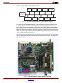
1
Application Note: Embedded Processing
Reference System: PLBv46 PCI Using the
ML410 Embedded Development Platform
R
Author: Lester Sanders
XAPP1001 (v1.0) February 8, 2008
Summary
This application note describes how to build a reference system for the Processor Local Bus
Peripheral Component Interconnect (PLBv46 PCI) core using the IBM PowerPC™ 405
(PPC405) Processor-based embedded system in the ML410 Embedded Development
Platform. The reference system is Base System Builder (BSB) based and uses ten peripherals.
A set of files containing Xilinx Microprocessor Debugger (XMD) commands is provided for
writing to the Configuration Space Headers and for verifying that the PLBv46 PCI core is
operating correctly. Several software projects illustrate how to configure the PLBv46 PCI
core(s), set up interrupts, scan configuration registers, and set up and use DMA operations.
The procedure for using ChipScope™ Pro Analyzer to analyze PLBv46 PCI and system
functionality is provided. The steps used to build a Linux kernel using MontaVista Linux™ are
listed.
Included
Systems
This application note includes one reference system:
www.xilinx.com/support/documentation/application_notes/xapp1001.zip
The project name in xapp1001.zip is ml410_ppc_plbv46_pci.
Required
Hardware and
Tools
Introduction
Users must have the following tools, cables, peripherals, and licenses available and installed.
EDK provides an evaluation license for PLBv46 PCI.
•
Xilinx EDK 9.2.02i
•
Xilinx ISE™ 9.2.04i
•
Xilinx Download Cable (Platform Cable USB or Parallel Cable IV)
•
Null modem serial cable,
•
Monta Vista Linux v4.0 Development Kit
•
Model Technology ModelSim v6.1e
•
ChipScope™ Pro Analyzer 9.2.01
•
PLBv46 PCI License
PCI transactions are done between an initiator and a target. This reference design is for the
ML410 Embedded Development Platform. To be useful, a target board should be inserted into
a PCI slot. In the examples provided in this application note, the ML555 Embedded
Development Platform is inserted into PCI slot P3 of the Xilinx ML410 Evaluation Platform. This
allows both configuration and memory transactions to be done on the PCI bus between an
initiator and a target. The examples use the ML410 PLBv46 PCI as the initiator and the ML555
PLBv46 PCI as the target. An Avnet Spartan-3 Evaluation board can be substituted for the
ML555 Embedded Development Platform.
© 2008 Xilinx, Inc. All rights reserved. XILINX, the Xilinx logo, and other designated brands included herein are trademarks of Xilinx, Inc. All other trademarks are the property
of their respective owners.
XAPP1001 (v1.0) February 8, 2008
www.xilinx.com
1
R
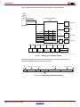
Introduction
Figure 1 is a block diagram of the reference system.
X-Ref Target - Figure 1
XPS_LL
TEMAC
XPS_
SYSACE
XPS_
INTC
XPS_UART
16550
XPS GPIO
PPC405
XPS
CENTRAL DMA
XPS
BRAM
PLBv46
PCI
XPS
IIC
MPMC
X1001_01_010708
Figure 1:
ML410 PLBv46 PCI Reference System Block Diagram
The system uses the embedded PowerPC as the microprocessor and the PLBv46 PCI core.
On the ML410 board, the Virtex-4 XC4VFX60 accesses two 33 MHz 32-bit PCI buses: a
primary 3.3V PCI bus and a secondary 5.0V PCI bus. The FPGA is directly connected to the
primary 3.3V bus. The 5.0V PCI bus is connected to the Primary PCI bus with a PCI-to-PCI
bridge, the TI2250. The PCI devices and four PCI add-in card slots on the ML410 are listed in
Table 2. All PCI bus signals driven by the XC4VFX60 comply with the I/O requirements in the
PCI Local Bus Specification, Revision 2.2.
PCI configuration in this reference design uses the ML410 PLBv46 PCI Bridge as a host bridge.
Figure 2 shows the ML410 with the Vmetro VG-PCI inserted into PCI slot P5 and the ML555
inserted into slot P3.
X-Ref Target - Figure 2
X1001_02_010708
Figure 2:
XAPP1001 (v1.0) February 8, 2008
ML410 with ML555, Vmetro VG-PCI in PCI Slots
www.xilinx.com
2
R
Introduction
Figure 3 shows PCI Bus Devices on the ML410. The TI2250 device is a PCI-to-PCI bridge to
the two 5V PCI slots. The ALi M1535D+ South Bridge interfaces to the legacy devices,
including the audio, modem, USB, and IDE ports. The Xilinx Virtex-5 ML555 Evaluation Board
is inserted into PCI slot P3.
X-Ref Target - Figure 3
PCI-to-PCI
5.0V
Bridge (U32)
3.3V
5.0V PCI Slot 6
PCI_S_CLK0
PCI_S_AD18 IDSEL
PCI_BUS
5.0V PCI Slot 4
PCI_S_CLK1
FPGA (U37)
IDSEL
PCI Bus
0xAC23 104C
PCI_P_AD24
PCI_P_AD25
PCI_P_CLK5
PCI_P_CLK4
PCI_P_CLK0
IDSEL
PCI_BUS
PCI_S_AD19 IDSEL
PCI_BUS
TI2250
3.3V PCI Slot 5
PCI_P_AD21
PCI_P_CLK1
PCI_P_CLK3
IDSEL
PCI_BUS
3.3V PCI Slot 3
PCI_P_AD22
IDSEL
PCI_BUS
ALi South Bridge (U15)
PCI_P_AD17
PCI_P_AD18
PCI_P_AD19
PCI_P_AD26
PCI_P_AD27
PCI_P_AD31
IDSEL
Audio
Dev ID Vend ID
0x5451 10B9
S. Bridge 0x1533 10B9
Modem
0x5457 10B9
USB#2
0x5237 10B9
IDE Bus 0x5229 10B9
USB#1
0x5237 10B9
PCI Bus
Figure 3:
XAPP1001 (v1.0) February 8, 2008
X1001_03_010708
PCI Bus Devices on the ML410
www.xilinx.com
3
R
Introduction
Figure 4 shows the connections of the South Bridge to the legacy devices.
X-Ref Target - Figure 4
FPGA
(U37)
PCI_P_AD24
IDSEL
PCI Bus
ALi South Bridge
(U15)
X4
PCI_P_CLK3
OSC
32.768 MHz
X2
OSC
PCI_P_AD17
PCI_P_AD18
PCI_P_AD19
PCI_P_AD26
PCI_P_AD27
PCI_P_AD31
IDSEL
Device ID
Vendor ID
Audio
0x5451
0x10B9
S. Bridge 0x1533
0x10B9
Modem
0x5457
0x10B9
USB#2
0x5237
0x10B9
IDE Bus
0x5229
0x10B9
USB#1
0x5237
0x10B9
48 MHz
X3
OSC
U1
X1
AC97
OSC
14.3181 MHz
24.576 MHz
PCI Bus
USB
1
USB
2
Parallel
Port
PS/2
Keyboard
GPIO
P1
P2
J5
J3
Flash
Primary IDE
Secondary IDE
U4
J16/J15
X1001_04_010708
Figure 4:
ALI Bus - PCI to Legacy Devices
The functions, devices, and buses in this reference design are addressed using the
Configuration Address Port format shown in Figure 5.
X-Ref Target - Figure 5
00
0 1 2
Doubleword
Bus No.
Function No.
7
8
10 11
15 16
Reserved
23 24
Device No.
Figure 5:
XAPP1001 (v1.0) February 8, 2008
E
30 31
X964_05_010708
Configuration Address Port Format
www.xilinx.com
4
R
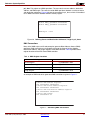
Reference System Specifics
The Configuration Address Port and Configuration Data Port registers in the Virtex-4 PLBv46
PCI Bridge are used to configure multiple PCI functions when host bridge configuration is
enabled.The bit definitions of the Configuration Address Port in the big endian format used by
the PLBv46 are given in Table 1.
Table 1: Configuration Address Port Register Definitions
Bit
Definition
0-5
Target word address in configuration space
6-7
Hardwired to 0
8-12
Device
13-15
Function
16-23
Bus Number
24
Enable
25-31
Reference
System
Specifics
Hardwired to 0
In addition to the PowerPC 405 processor and PLBv46 PCI, this system includes DDR2 and
BRAM memory, UART, interrupt controller, SYSACE, IIC, and GPIO. The modules are shown in
Figure 1. The PCI Arbiter core is included in the FPGA.
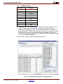
The addresses of the IDSEL lines on the ML410 Board are listed in Table 2.
Table 2: ML410 PCI Devices – IDSEL Lines
Dev ID
Vend ID
Bus
Dev
IDSEL
Address
FPGA
0x0410
0x10EE
0
8
AD24
Ali M1535D+ South Bridge
0x1533
0x10B9
0
2
AD18
ALi IDE
0x5529
0x10B9
0
11
AD27
ALi Audio
0x5451
0x10B9
0
11
AD17
ALi Modem
0x5457
0x10B9
0
3
AD19
ALi USB#1
0x5237
0x10B9
0
15
AD31
ALi USB#2
0x5237
0x10B9
0
10
AD26
TI Bridge (TI2250)
0AC23
0x104C
0
9
AD25
3.3V PCI Slot 3
N/A
N/A
3.3V PCI Slot 5
N/A
N/A
0
5
AD21
5.0V PCI Slot 4
N/A
N/A
1
3
AD19
5.0V PCI Slot 6
N/A
N/A
1
2
AD18
Device
XAPP1001 (v1.0) February 8, 2008
www.xilinx.com
AD22
5
R
Reference System Specifics
ML410 XC4VFX60 Address Map
The address map of the ML410 XC4VFX60 is listed in Table 3.
Table 3: ML410 XC4VFX60 System Address Map
Peripheral
Instance
Base Address
High Address
MPMC
DDR_SDRAM
0x00000000
0x03FFFFFF
XPS UART16550
RS232_Uart_1
0x83E00000
0x83E0FFFF
XPS INTC
XPS_intc_0
0x81800000
0x8180FFFF
PLBv46 PCI
PCI32_Bridge
0x85E00000
0x85E0FFFF
XPS Central DMA
xps_central_dma_0
0x80200000
0x8020FFFF
XPS BRAM
xps_bram_if_cntlr_0
0xFFFF0000
0xFFFFFFFF
XPS SYSACE
SysACE_CompactFlash
0x83600000
0x8360FFFF
XPS GPIO
LEDs_8Bit
0x81400000
0x8140FFFF
XPS IIC
IIC_Bus
0x81600000
0x8160FFFF
XPS_LL_TEMAC
TriMode_MAC_MII
0x81C000000
0x81C0FFFF
The reference design contains the following settings for PLBv46 PCI generics. Generics are
parameters that are used in VHDL to configure the design.
C_FAMILY = virtex4
C_INCLUDE_PCI_CONFIG = 1
C_INCLUDE_BAROFFSET = 0
C_IPIFBAR_NUM = 2
C_PCIBAR_NUM = 2
C_IPIFBAR_0 = 0x20000000
C_IPIFBAR2PCIBAR_0 = 0x80000000
C_IPIFBAR_1 = 0xE8000000
C_IPIFBAR2PCIBAR_1 = 0x90000000
When C_FAMILY is defined as Virtex4 or Spartan3, the PLBv46 PCI uses the v3.0 PCI
LogiCORE IP. When C_FAMILY is defined as Virtex5, the PLBv46 PCI uses the v4.0 PCI
LogiCORE IP.
XAPP1001 (v1.0) February 8, 2008
www.xilinx.com
6
R
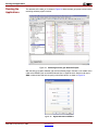
Reference System Specifics
Figure 6 shows how to specify the values of the Base Address Register (BAR) generics in EDK.
To get this screen, double click on PLBv46 PCI in the System Assembly View.
X-Ref Target - Figure 6
X1001_06_010708
Figure 6: Specifying the Values of Generics in EDK
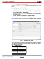
Implementation Results
The resource utilization in the reference design is shown in Table 4.
Table 4: Design Resource Utilization
Resources
Used
Available
Utilization (%)
Slice registers
8475
50560
16
Slice LUTs
11259
50560
22
DCM_ADV
1
12
8
Block RAM
57
232
24
Setting C_INCLUDE_PCI_CONFIG = 1 configures the bridge as a host bridge. When
C_INCLUDE_BAR_OFFSET = 0, the C_IPIFBAR2PCIBAR_* generic(s) are used in address
translation instead of IPIFBAR2PCIBAR_* registers. Setting C_IPIFBAR_NUM = 2 specifies
that there are two address ranges for PLB to PCI transactions. Setting C_PCIBAR_NUM = 2
specifies that two address ranges are used for PCI to PLB transactions.
XAPP1001 (v1.0) February 8, 2008
www.xilinx.com
7
R
Reference System Specifics
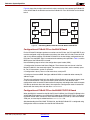
Figure 7 provides a functional diagram of the PLBv46 PCI core. The functions in the PLBv46
PCI are the PLBv46 Master, PLBv46 Slave, v3.0 (v4.0) PCI Core, and the IPIF/v3.0 (v4.0)
Bridge.
X-Ref Target - Figure 7
PLBv46
Master
IPIF/V3
Bridge
PLBV46
V3
PCI Core
PCI
PLBv46
Slave
X1001_07_010708
Figure 7:
PLBv46 PCI Functional Diagram
ML555 PCI/PCI Express Evaluation Platform
In the reference design, the PLBv46 PCI in the XC4VFX60 on the ML410 board interfaces to
the PLBv46 PCI in the Virtex-5 ML555 PCI/PCI Express Embedded Development Platform.
This operates on a 32-bit PCI bus. The ML555 board uses the Xilinx XC5VLX50T device in the
1136 pin package.
The address map for the XC5VLX50T is listed in Table 5.
Table 5: ML555 Address Map
Peripheral
Instance
Base Address
High Address
LMB BRAM IF CNTLR
DLMB_CNTLR/ILMB_CNTLR
0x0000000
0x00001FFF
XPS UARTLITE
RS232_Uart_1
0x84000000
0x8400FFFF
PLBv46 PCI
plbv46_pci_0
0x42600000
0x4260FFFF
MPMC
DDR_SDRAM_64Mx32
0x90000000
0x9FFFFFFF
XPS GPIO
LEDs_8Bit
0x81400000
0x8140FFFF
MDM
debug_module
0x84400000
0x8440FFFF
XPS INTC
xps_intc_0
0x80200000
0x8020FFFF
XPS CENTRAL DMA
xps_central_dma_0
0x81810000
0x8181FFFF
XPS BRAM CNTLR
xps_bram_if_cntlr_1
0x8A208000
0x8A20FFFF
The ML555 includes a 64-bit PCI edge connector, 128 MB (or 256 or 512 MB) DDR2 SDRAM
memory, RS232C port, LED displays, XCF32P-FSG48C Platform Flash configuration PROM,
and a JTAG port. The MicroBlaze microprocessor is used.
The application note, XAPP999 Reference System: PLBv46 PCI in a ML555 Embedded
Development Platform, provides a link to the ML555 system.
XAPP1001 (v1.0) February 8, 2008
www.xilinx.com
8
R
Reference System Specifics
Figure 8 shows the principle interface blocks when transferring data between the PLBv46 PCI
in the XC4VFX60 on the ML410 board and the PLBv46 PCI in the XC5VLX50T on the ML555
board.
X-Ref Target - Figure 8
ML410
ML555 - Slot P3
DDR
PPC
DDR
PLBv46
PCI
PLBv46
PCI
BRAM
MB
BRAM
X1001_08_010708
Figure 8: Interfacing ML410 PLBv46 PCI with ML555 PLBv46 PCI
Configuration of PLBv46 PCI on the ML410 Board
For the PLBv46 PCI bridge to perform transactions on the PCI bus, the PCI LogiCORE IP v3.0
must be configured using configuration transactions from either the PCI-side or from the PLB
side. In this reference design, the ML410 PLBv46 PCI is the host bridge, configured from the
PLB side. The v3.0 IDSEL input is connected to the address ports specified in Table 2, and the
IDSEL port of the PLBv46 PCI is unused.
Use the following steps to write to the configuration space header (CSH).
1. Configure the Command and Status Register. The minimum that must be set is the Bus
Master Enable bit in the command register. For memory transactions, set the memory space
bit. For I/O transactions, set the I/O space bit.
2. Configure the Latency Timer to a non-zero value, usually 0xFF.
3. Configure at least one BAR. Configure additional BARs as needed for other memory/IO
address ranges.
The v3.0 core configures itself only after the Bus Master Enable bit is set and the latency timer
is set to avoid time-outs. If the v3.0 core latency timer remains at the default 0 value,
configuration writes to remote PCI devices do not complete, and configuration reads of remote
PCI devices terminate due to the latency timer expiration. Configuration reads of remote PCI
devices with the latency timer set to 0 return 0xFFFFFFFF.
Configuration of PLBv46 PCI on the ML555 PCI/PCI-X Board
When the ML555 is inserted into the ML410 PCI slot P3 (AD22), the PLBv46 PCI Bridge in the
XC4VFX60 FPGA interfaces to an PLBv46 PCI Bridge in the XC5VLX50T FPGA. To configure
the ML555 XC5VLX50T, connect the Xilinx Download (USB or Parallel IV) cable to the ML555
JTAG port, and use Impact to download the download.bit file.
After downloading the XC5VLX50T FPGA bit file, the ML555 PLBv46 PCI is configured using
Configuration write transactions from the ML410 PLBv46 PCI.
XAPP1001 (v1.0) February 8, 2008
www.xilinx.com
9
R
Reference System Specifics
Executing the Reference System using the Pre-Built Bitstream and the
Compiled Software Applications
Use the steps below to execute the system using files in the
ml410_ppc_plbv46_pci/ready_for_download directory.
1. Change to the ml410_ppc_plbv46_pci/ready_for_download directory.
2. Use iMPACT to download the bitstream.
impact -batch xapp1001.cmd
3. Invoke XMD. Connect to the PPC405 processor and reset.
xmd
connect ppc hw
rst
4. Download the executable.
dow ml410_ppc_plbv46_pci/ready_for_download/pci_dma.elf
Executing the Reference System from EDK
Use the steps below to execute the system using XPS.
1. Select File → Open system.xmp in XPS.
2. Use Hardware → Generate Bitstream to generate a bitstream.
3. Use Device Configuration → Update Bitstream to add bootloop to bitstream
4. Download the bitstream to the board using Device Configuration → Download
Bitstream.
5. Right click the Software Project (e.g. pci_dma) and Build Project
6. Invoke XMD with Debug Launch → XMD.
7. Download the executable by the following command.
dow ml410_ppc_plbv46_pci/pci_dma/executable.elf
Verifying the Reference Design with the Xilinx Microprocessor
Debugger
After downloading the bitstream file and writing to the configuration header, verify that the
ML410 reference design is set up correctly.
1. Configure the v3.0 Command Register, Latency Timer, and BAR(s).
2. Read the configuration header.
3. Configure the Command Register, Latency Timer, and BAR(s) of the other devices in the
system.
4. Read the configuration headers of the other devices in the system.
5. Perform a memory read of one of the IPIF BARs.
6. Perform a memory write of one of the IPIF BARs.
Verification is done using either Xilinx Microprocessor Debugger (XMD) or the software projects
discussed later. TCL scripts of the XMD commands are provided in
ml410_ppc_plbv46_pci/xmd_commands. The 410_555.tcl script configures and verifies the
ML410 and ML555 PCI cores. To run this script, enter
xmd -tcl xmd_commands/410_555.tcl
at the command prompt.
XAPP1001 (v1.0) February 8, 2008
www.xilinx.com
10
R
Reference System Specifics
The XMD commands in the 410_555.tcl file, partially listed in Figure 9, write to the
Configuration Address Port and to the Configuration Data Port to program the Configuration
Space Headers. The Command/Status Register, Latency Timer, and Base Address Registers
of the ML410 and ML555 PLBv46 PCIs are written and read.
X-Ref Target - Figure 9
X1001_09_010708
Figure 9:
Excerpts from 410_555.tcl
Software Projects
The reference system contains the following software projects.
hello_pci. This project enables master transactions, sets the latency timer, defines the bus
number/subordinate bus number, and scans the PCI bus configuration space headers.
XAPP1001 (v1.0) February 8, 2008
www.xilinx.com
11
R
Reference System Specifics
pci_dma. This project runs DMA operations. The user sets the source address, destination
address, and DMA length. This code is used for DMA operations between a variety of source
and destination addresses. Figure 10 shows the parameters in pci_dma.c which can be edited
to run DMA transactions between different memory regions.
X-Ref Target - Figure 10
define MEM_0_BASEADDR 0x20000000
define MEM_1_BASEADDR 0x20002000
..
DMALength = 1024
X1001_10_010708
Figure 10:
Defining Source and Destination Addresses, Length in pci_dma.c
DMA Transactions
Many of the XMD scripts and C code examples generate Direct Memory Access (DMA)
operations. DMA transactions are initiated by writing to the Control, Source Address,
Destination Address, and Length registers of the DMA controller. Table 6 provides these
register locations of the XPS Central DMA controller.
Table 6: DMA Register Locations
DMA Register
Address
Control Register
C_BASEADDR + 0x04
Source Address Register
C_BASEADDR + 0x08
Destination Address Register
C_BASEADDR + 0x0C
Length Register
C_BASEADDR + 0x10
An example of XMD code which generates DMA transactions is given in Figure 11.
X-Ref Target - Figure 11
# Write DMA Control Register
mwr 0x80200004 0xC0000004
# Write DMA Source Address Register
mwr 0x80200008 0x20000000
# Write DMA Destination Address Register
mwr 0x8020000C 0x20002000
# Write DMA Length
mwr 0x80200010 64
X1001_11_010708
Figure 11:
XAPP1001 (v1.0) February 8, 2008
Generating DMA Transactions
www.xilinx.com
12
R
Reference System Specifics
The pci_dma.c code consists of the four functions in the functional diagram in Figure 12. The
Barberpole Region function provides a rotating data pattern on the memory located at the
source address. The Zero Region function sets the memory located at the destination address
to all zeroes. The DMA Region function performs a DMA transaction of data located at the
source address to the memory at the destination address. The Verify function verifies that data
at the source address and destination address are equal.
X-Ref Target - Figure 12
Barberpole
Region
Zero
Region
DMA
Region
Verify
X1001_12_010708
Figure 12:
Functional diagram of pci_dma.c
Figure 13 show the Hyperterminal output when running the pci_dma/executable.elf. The
program is run twice, initially with a length of 100, then with a length of 400.
X-Ref Target - Figure 13
X1001_13_010708
Figure 13:
XAPP1001 (v1.0) February 8, 2008
www.xilinx.com
pci_dma.c Output
13
R
Running the Applications
Running the
Applications
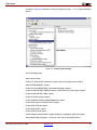
The selection of the hello_pci is shown in Figure 14. Make the hello_pci project active and the
remaining software projects inactive.
X-Ref Target - Figure 14
X1001_14_010708
Figure 14:
Selecting the hello_pci Software Project
With the hello_pci project selected, right click to build the project. Connect a null modem serial
cable to the RS232C port on the ML410 board. Start a HyperTerminal. Set the baud rate to
9600, number of data bits to 8, no parity, and no flow control, as shown in Figure 15.
X-Ref Target - Figure 15
X1001_15_010708
Figure 15: HyperTerminal Parameters
XAPP1001 (v1.0) February 8, 2008
www.xilinx.com
14
R
Using ChipScope with PLBv46 PCI
From XPS, start XMD and enter connect ppc hw and rst at the XMD prompt. Invoke GDB
and select Run to start the application as shown in Figure 16. The hello_pci.c code, originally
written for the OPB PCI used on a ML310, runs without modifications on this reference system.
X-Ref Target - Figure 16
X1001_16_010708
Figure 16:
Using
ChipScope with
PLBv46 PCI
Running hello_pci in GDB
ChipScope is used to debug hardware problems. Debugging can be done at either the system
or PLBv46 PCI core level. To analyze PLBv46 PCI internal signals, insert the ChipScope cores
into pci32_bridge_wrapper.ngc. To analyze signals involving multiple cores, insert the
ChipScope cores into system.ngc. The flow for using the two debugging methods differs.
Below, an outline of the steps for debugging at the system level is provided. This is followed by
a detailed list of steps for debugging at the core level.
Inserting ChipScope at the System Level
The following steps insert the ChipScope cores into the system.
1. In XPS, select Hardware → Generate Netlist.
2. From the command prompt in the implementation directory, run
ngcbuild -i system.ngc system2.ngc
3. Invoke ChipScope Inserter. To specify the input in the Input Design Netlist window,
browse to the system2.ngc file created in step 2. Define the Clock, Trigger, and Data
signals in Inserter, and generate the ICON and ILA cores. The
chipscope/ml410_ppc_plbv46_pci_scs.cdc file provides signals from the PLBv46
PCI and XPS Central DMA Controller as an example.
4. From ml410_ppc_plbv46_pci/implementation, copy the file displayed in the Inserter Output
Design Netlist window, usually implementation/system2.ngo, to
implementation/system.ngc.
XAPP1001 (v1.0) February 8, 2008
www.xilinx.com
15
R
Using ChipScope with PLBv46 PCI
5. In XPS, run Hardware → Generate Bitstream.
The ml410_ppc_plbv46_pci_scs.cpj is provided in the chipscope directory for Analyzer
projects.
Inserting ChipScope in the PLBv46 PCI Core
The ml410_ppc_plbv46_pci/chipscope/plbv46_pci_ccs.cdc file is used to insert a
ChipScope ILA core into the ML410 PLBv46 PCI Bridge wrapper (pci32_bridge_wrapper) core.
Do the following steps to insert a core and analyze PLBv46 PCI problems with ChipScope.
1. Invoke XPS. Run Hardware → Generate Netlist.
2. Copy chipscope/plbv46_pci_ccs.cdc file to the project area (one directory above
the chipscope directory).
3. Run Start → Programs → ChipScope Pro → ChipScope Inserter
4. From ChipScope Inserter, run File Open → plbv46_pci_ccs.cdc.
Figure 17 shows the ChipScope Inserter setup GUI after File Open → plbv46_pci_ccs.cdc.
X-Ref Target - Figure 17
X1001_17_010708
Figure 17: ChipScope Inserter Setup
The PCI_Monitor signals are the PCI bus signals: AD, CBE, and the remaining PCI Bus signals.
Table 7 defines the functionality of the PCI_Monitor signals. The Filter Pattern *PCI_Monitor* is
used to locate the PCI bus signals.
Table 7: PCI Monitor Signals
Bit Position
PCI Signal
0
FRAME_N
1
DEVSEL_N
2
TRDY_N
3
IRDY_N
4
STOP_N
XAPP1001 (v1.0) February 8, 2008
www.xilinx.com
16
R
Using ChipScope with PLBv46 PCI
Table 7: PCI Monitor Signals
Bit Position
PCI Signal
5
IDSEL_int
6
INTA
7
PERR_N
8
SERR_N
9
Req_N_toArb
10
PAR
11
REQ_N
12:43
AD
44:47
CBE
5. The plbv46_pci_ccs.cdc provides a good starting point for analyzing designs. In some
analyses, additional nets are needed. Figure 18 shows the GUI for making net
connections. Click Next four times to move to the Modify Connections window. Select
Modify Connections. The Filter Pattern is used to find net(s). As an example of using the
Filter Pattern, enter *ack* in the dialog box to locate acknowledge signals such as
Sl_AddrAck. In the Net Selections area, select either Clock, Trigger, or Data Signals. Select
the net and click Make Connections.
The correct Clock, Trigger, and/or Data signals displayed in red.
X-Ref Target - Figure 18
X1001_18_010708
Figure 18:
XAPP1001 (v1.0) February 8, 2008
Making Net Connections in ChipScope Inserter
www.xilinx.com
17
R
Using ChipScope with PLBv46 PCI
6. Click Insert to insert the core into pci32_bridge_wrapper.ngo. In the
ml410_ppc_plbv46_pci/implementation directory, copy
pci32_bridge_wrapper.ngo to pci32_bridge_wrapper.ngc.
7. In XPS, run Hardware → Generate Bitstream and Device Configuration → Download
Bitstream. Do not rerun Hardware → Generate Netlist, as this overwrites the
implementation/pci32_bridge_wrapper.ngc produced by the step above. Verify
that the file size of the pci32_bridge_wrapper.ngc with the inserted core is significantly
larger than the original version.
8. Invoke ChipScope Pro Analyzer by selecting
Start → Programs → ChipScope Pro → ChipScope Pro Analyzer
Click on the Chain icon located at the top left of the Chipscope Analyzer’s GUI. Verify that the
message in the transcript window indicates that an ICON is found.
9. The ChipScope Analyzer waveform viewer displays signals named DATA*. To replace the
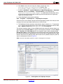
DATA* signal names with the familiar signal names specified in ChipScope Inserter, select
File → Import and browse to plbv46_pci_ccs.cdc in the dialog box.
The Analyzer waveform viewer is more readable when buses rather than discrete signals are
displayed. Select the 32 PLB_ABus<*> signals, click the right mouse button, and select Add to
Bus → New Bus. With PLB_ABus<0:31> in the waveform viewer, select and delete the 32
discrete PLB_ABus<*> signals. Repeat this for the PLBv46 data buses. Make PCI Bus signals
by creating a new bus for PCI_Monitor(44:47), then rename it to PCI_Monitor(44:47) PCI_CBE.
Create a new bus for PCI_Monitor(12:43), then rename it to PCI_Monitor(12:43) PCI_AD. The
signals are displayed as buses in Figure 19.
Note: The Reverse Bus Order operation is useful for analyzing buses in Analyzer.
X-Ref Target - Figure 19
X1001_19_010708
Figure 19:
XAPP1001 (v1.0) February 8, 2008
Creating Buses in ChipScope Analyzer
www.xilinx.com
18
R
Using ChipScope with PLBv46 PCI
10. Set the trigger in the Trigger Setup window. The trigger used depends on the problem being
debugged. For example, if debugging a configuration transaction from the ML410 PLBv46
PCI, trigger on an PLBv46 address of C_BASEADDR + 0x10C. If debugging a problem
configuring from the PCI side, trigger on the PCI_CBE for a configuration write on CBE.
Simpler triggers are PCI_FRAME_N (PCI_Monitor_0) on the PCI side and PA_Valid or
Sl_AddrAck on the PLBv46 side.
11. Arm the trigger by selecting Trigger Setup → Arm, or clicking on the Arm icon.
12. Run XMD or GDB to trigger patterns which cause ChipScope to display waveform output.
For example, set the trigger to PA_Valid, arm the trigger, and run
xmd -tcl xmd_commands/410_555.tcl
at the command prompt. This produces signal activity in the Analyzer waveform viewer.
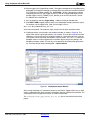
13. ChipScope results are analyzed in the waveform window, as shown in Figure 20. This
figure shows the bus signals generated in step 9 above. To share the results with remote
colleagues, save the results in the waveform window as a Value Change Dump (vcd) file.
The vcd files can be translated and viewed in most simulators. The vcd2wlf translator in
ModeSim reads a vcd file and generates a waveform log file (wlf) file for viewing in the
ModelSim waveform viewer. The vcd file can be opened in the Cadence Design System,
Inc. Simvision design tool by selecting File → Open Database.
X-Ref Target - Figure 20
X1001_20_010708
Figure 20: ChipScope Analyzer Results
After running ChipScope, it is sometimes necessary to revise the Trigger or Data nets, or both,
used in a debug operation. Saving Inserter and Analyzer projects simplifies this procedure. The
saved project can be re-opened in Inserter, and edits can be made.
The chipscope/ml410_ppc_plbv46_pci_ccs.cpj file can be used for the Analyzer
project.
XAPP1001 (v1.0) February 8, 2008
www.xilinx.com
19
R
Linux Kernel
Linux Kernel
XAPP765 Getting Started with EDK and Monta Vista Linux introduces Monta Vista Linux to
new users. The steps to build and boot a Linux kernel are given below. Steps 1-3, 7, 8 are run
on a Linux machine with MontaVista Professional Edition installed.
1. Add /opt/montavista/pro/host/bin and
/opt/montavista/pro/devkit/ppc/405/bin
to $PATH.
2. Create and change to the ml410_ppc_plbv46_pci/linux directory.
3. Run
tar cf - -C /opt3/montavista/pro/devkit/lsp/xilinx-ml40xppc_405/linux-2.6.10_mvl401/ . | tar xf 4. To generate the Linux LSP in XPS, enter Software → Software Platform Settings. Select
Kernel and Operating Systems, then select OS: linux_2_6 and Version: 1.00.b.
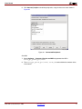
5. Under OS and Libraries, set the entries as shown in Figure 21.
X-Ref Target - Figure 21
X1001_21_010708
Figure 21:
Software Platform Setting Setup
Verify that the target directory is the same as the directory containing the Linux source.
XAPP1001 (v1.0) February 8, 2008
www.xilinx.com
20
R
Linux Kernel
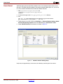
6. Click Connect_Periphs and add the peripherals, using the instance names shown in
Figure 22.
X-Ref Target - Figure 22
X1001_22_010708
Figure 22:
Connected Peripherals
Click OK.
7. Select Software → Generate Libraries and BSPs to generate the LSP in
ml410_ppc_plbv46_pci/linux.
8. The ml410_ppc_plbv46_pci/linux/.config is used to define the contents of the
Linux kernel.
XAPP1001 (v1.0) February 8, 2008
www.xilinx.com
21
R
Linux Kernel
As shown in Figure 23, enter make xconfig and generate a new .config using the following
options.
X-Ref Target - Figure 23
X1001_23_010408
Figure 23:
Running make xconfig
Run the following steps.
Select General Setup
Enable PCI. Disable PS/2 keyboard. Change to /dev/ram for booting from ramdisk.
Select ATA/IDE/MFM/RLL support.
Enable Enhanced IDE/MFM/RLL disk/cdrom/tape/floppy support.
Enable Include IDE/ATAPI CDROM support. Enable Generic PCI IDE chipset support.
Enable Include IDE/ATA-2 DISK support.
Enable ALI M15x3 chipset support.
Enable PROMISE PDC202 {46|62|65|68|69|70} support.
Enable SCSI support. Enable SCSI disk support.
Enable SCSI CD-ROM support.
Enable SCSI generic support.
Enable SCSI low-level drivers.
Enable Adaptec AHA152X/2825, Adaptec AHA1542, and Adaptec AHA1740 support.
Select Network Device Support → Ethernet (10 or 100), enable 3Com devices.
XAPP1001 (v1.0) February 8, 2008
www.xilinx.com
22
R
Linux Kernel
Enable Vortex if using the 3Com PCI card.
Enable EISA, VLB, PCI and on board controllers.
Enable DECchip Tulip (dc2lx4x) PCI, support, EtherExpressPro/100 support, National
Semiconductor DB8381x..., and SMC EtherPowerII
Select Console Drivers. Disable Frame Buffer Support.
Select Input Core Support. Disable all.
Select Character Devices. Disable Virtual. Leave Serial enabled. Disable Xilinx GPIO and
Touchscreen.
Enable USB support.
Run make zImage.initrd. Verify that the zImage.initrd.elf file is in the
ml410_ppc_plbv46_pci/linux/arch/ppc/boot/images directory.
9. Use Impact to download implementation/download.bit to XC4VFX60. Either select
Device Configuration → Download Bitstream from XPS or run the following command
from the command prompt:
impact -batch etc/download.cmd
10. Invoke XMD. From the ml410_ppc_plbv46_pci/linux directory, enter the following
commands in the XMD window:
rst
dow arch/ppc/boot/images/zImage.initrd.elf
con
11. The HyperTerminal window displays the Linux boot process. Login as root. Enter cd /
and ls -l to view the contents of the mounted Linux partition.
12. Enter ./lspci -vv to view the PCI devices. For each line of output, the first 2 digits
represent the PCI bus number, followed by the device number and function number.
13. An alternative to downloading the Linux kernel executable is to load it into CompactFlash.
The file used uses an ace file extension. To generate an ace file, run the command below
from the ml410_ppc_plbv46_pci directory.
xmd -tcl ../genace.tcl -jprog -hw ../implementation/system.bit -ace
../implementation/ace_system_hw.ace -board ML410
Copy the ace file to a 64-512 MB CompactFlash (CF) card in a CompactFlash reader/writer.
Remove the CF card from the CF reader/writer and insert it into the CompactFlash slot (J22) on
the ML410 board. Power up the board, and view Linux booting in the HyperTerminal window.
XAPP1001 (v1.0) February 8, 2008
www.xilinx.com
23
R
Reference Design Matrix
Reference
Design Matrix
The reference design matrix is shown in Table 8.
Table 8: Reference Design Matrix
General
Developer Name
Xilinx
Target devices (stepping level, ES, production, speed grades)
Source code provided
Virtex-4 XC4VTFX60
No
Source code format
VHDL
Design uses code/IP from an existing reference design/application
note, 3rd party, or CORE Generator software
No
Simulation
Functional simulation performed
No
Timing simulation performed
No
Testbench used for functional simulations provided
No
Testbench format
N/A
Simulator software used/version (i.e., ISE software, Mentor,
Cadence, other)
N/A
SPICE/IBIS simulations
No
Implementation
Synthesis software
XST
Implementation software tools used/versions
Static timing analysis performed
ISE9.2i SP3
Yes
Hardware Verification
Hardware verified
Yes
Hardware platform used for verification
References
ML410/ML555
1. DS207 PCI 64/32 Interface v3.0 Data Sheet
2. UG159 LogiCORE IP Initiator/Target v3.1 for PCI
3. UG262 LogiCORE IP Initiator/Target v4.5 for PCI
4. UG085 ML410 Embedded Development Platform User Guide
5. UG044 ChipScope ILA Tools Tutorial
6. UG201 Virtex-5 ML555 Development Kit for PCI/PCI Express Designs User Guide
7. UG241 OPB PCI v1.02a User Manual
8. XAPP765 Getting Started with EDK and MontaVista Linux
9. XAPP999 Reference System: PLBv46 PCI Using the ML555 Embedded Development
Platform
10. XAPP1038 Reference System: PLBv46 PCI Using the Avnet Spartan-3 Evaluation Board
11. XAPP998 PCI Bus Performance Measurements using the Vmetro Bus Analyzer
XAPP1001 (v1.0) February 8, 2008
www.xilinx.com
24
R
Revision History
Revision
History
Notice of
Disclaimer
The following table shows the revision history for this document.
Date
Version
2/8/08
1.0
Revision
Initial Xilinx release.
Xilinx is disclosing this Application Note to you “AS-IS” with no warranty of any kind. This Application Note
is one possible implementation of this feature, application, or standard, and is subject to change without
further notice from Xilinx. You are responsible for obtaining any rights you may require in connection with
your use or implementation of this Application Note. XILINX MAKES NO REPRESENTATIONS OR
WARRANTIES, WHETHER EXPRESS OR IMPLIED, STATUTORY OR OTHERWISE, INCLUDING,
WITHOUT LIMITATION, IMPLIED WARRANTIES OF MERCHANTABILITY, NONINFRINGEMENT, OR
FITNESS FOR A PARTICULAR PURPOSE. IN NO EVENT WILL XILINX BE LIABLE FOR ANY LOSS OF
DATA, LOST PROFITS, OR FOR ANY SPECIAL, INCIDENTAL, CONSEQUENTIAL, OR INDIRECT
DAMAGES ARISING FROM YOUR USE OF THIS APPLICATION NOTE.
XAPP1001 (v1.0) February 8, 2008
www.xilinx.com
25