1
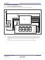
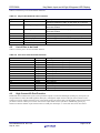
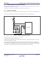
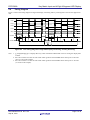
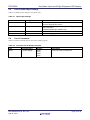
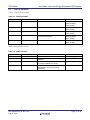
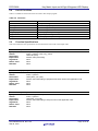
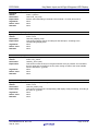
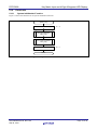
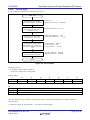
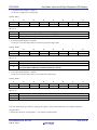
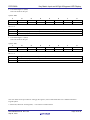
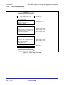
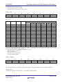
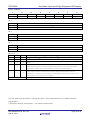
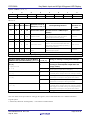
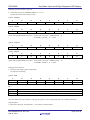
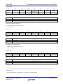
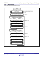
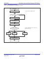
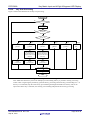
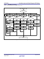
APPLICATION NOTE R7F0C809 Key Matrix Input and 4-Digit 8-Segment LED Display R01AN2006EC0100 Rev.1.00 Sep 30, 2014 Introduction This application note describes a method about how to use the key matrix input and the 4-digit 8-segment LED display with the R7F0C809 microcontroller. Target Device R7F0C809 When applying the sample program covered in this application note to another microcomputer with the same SFR (Special Function Register), modify the program according to the specifications for the target microcomputer and conduct an extensive evaluation of the modified program. R01AN2006EC0100 Rev.1.00 Sep 30, 2014 Page 1 of 30 R7F0C809 Key Matrix Input and 4-Digit 8-Segment LED Display Contents 1. Specifications .................................................................................................................3 2. Operating Conditions ..................................................................................................... 4 3. Related Application Note ............................................................................................... 4 4. Description of the Hardware .......................................................................................... 5 4.1 Hardware Configuration Example ............................................................................................. 5 4.2 List of Pins to be Used ............................................................................................................... 6 4.3 High Current I/O Port Function .................................................................................................. 6 5. Description of Software ................................................................................................. 7 5.1 Operation Overview .................................................................................................................... 7 5.2 4-Digit 8-Segment LED Display controlling .............................................................................. 8 5.3 Key Scan controlling .................................................................................................................. 8 5.4 Timing Diagram ........................................................................................................................... 9 5.5 List of Option Byte Settings ..................................................................................................... 10 5.6 List of Constants ....................................................................................................................... 10 5.7 List of Variables ........................................................................................................................ 11 5.8 List of Functions ....................................................................................................................... 12 5.9 Function Specifications ............................................................................................................ 12 5.10 Flowcharts ................................................................................................................................. 14 5.10.1 System Initialization Function ............................................................................................... 14 5.10.2 I/O Port Setup ....................................................................................................................... 15 5.10.3 Timer Array Unit Setup ......................................................................................................... 19 5.10.4 Main Processing.................................................................................................................... 26 5.10.5 LED Display Processing ....................................................................................................... 27 5.10.6 Key Scan Processing ............................................................................................................ 28 5.10.7 LED Mode Processing .......................................................................................................... 29 6. Sample Code ................................................................................................................ 30 7. Reference Documents.................................................................................................. 30 R01AN2006EC0100 Rev.1.00 Sep 30, 2014 Page 2 of 30 R7F0C809 1. Key Matrix Input and 4-Digit 8-Segment LED Display Specifications This application note describes how the high current I/O ports of R7F0C809 MCU control the LED COM pins and are used as key scan output pins. The channel 0 of Timer Array Unit 0 (TAU0) is used to generate a time interval to switch the COM pins and the channel 1 of Timer Array Unit 0 is used to generate a time delay to wait for the stability of the COM port voltage when it is changed from high level to low level. P00 and P16 pins are used as key scan input ports. Table 1.1 lists the peripheral functions and their applications. Table 1.1 Peripheral Functions and Their Applications Peripheral Function TAU0 channel 0 TAU0 channel 1 P02 to P05 P06,P07,P10 to P15 P00,P16 R01AN2006EC0100 Rev.1.00 Sep 30, 2014 Use Generate a time interval to switch the COM pins (Control the time interval of LED display scanning). Generate a time delay to wait for the stability of COM voltage. Control the LED COM ports and be used as key scan output ports. Control the LED SEG ports. Key scan input ports. Page 3 of 30 R7F0C809 2. Key Matrix Input and 4-Digit 8-Segment LED Display Operating Conditions The sample code contained in this application note has been tested under the conditions below. Table 2.1 Operation Confirmation Conditions Item MCU used Operating frequency Operating voltage Integrated development environment C compiler 3. Contents R7F0C809 • High-speed on-chip oscillator clock (fHOCO): 20 MHz (typ.) • CPU/peripheral hardware clock (fCLK): 20 MHz 5.0 V (operation enabled from 4.5 to 5.5 V) SPOR detection operation (VSPOR): rising edge 4.28V(typ.), falling edge 4.00V(min.) Renesas Electronics Corporation CubeSuite+ V2.01.00 Renesas Electronics Corporation CA78K0R V1.60 Related Application Note The application notes that are related to this application note are listed below for reference. • R7F0C809 6-Digit 8-Segment LED Display (R01AN2005E) Application Note • R7F0C809 4-Digit 8-Segment LED Display with A/D Key Read (R01AN2007E) Application Note R01AN2006EC0100 Rev.1.00 Sep 30, 2014 Page 4 of 30 R7F0C809 4. Key Matrix Input and 4-Digit 8-Segment LED Display Description of the Hardware 4.1 Hardware Configuration Example Figure 4.1 shows an example of hardware configuration that is used for this application note. VDD RESET P00 P40/TOOL0 P16 P15 P02 P14 P13 P03 P04 Used for on-chip debugging R7F0C809 P05 P12 P11 P10 VDD P07 K4 K3 K2 K1 VDD P06 VSS R K8 K7 K6 K5 SEG_dp SEG_g COM_1 COM_2 COM_3 COM_4 SEG_f SEG_e SEG_d SEG_c SEG_b SEG_a Figure 4.1 Hardware Configuration Notes:1. The purpose of this circuit is only to provide the connection outline and the circuit is simplified accordingly. When designing and implementing an actual circuit, provide proper pin treatment and make sure that the hardware's electrical specifications are met (connect the input-dedicated ports separately to VDD or VSS via a resistor). 2. VDD must be held at not lower than the reset release voltage (VSPOR) that is specified as SPOR. R01AN2006EC0100 Rev.1.00 Sep 30, 2014 Page 5 of 30 R7F0C809 Key Matrix Input and 4-Digit 8-Segment LED Display Table 4.2 lists the keys to be used and their functions. Table 4.1 Keys to be Used and Their Functions Key Name K1 Function LED all blink mode K2 LED ring shift right mode K3 LED ring shift left mode K4 K5 K6 K7 K8 Reserved Update display data Reset display data Reserved Reserved 4.2 Description After the key pressed, the LEDs will start blinking. The interval time between LEDs on and LEDs off is constant. After the key pressed, the display data rotate right at the same interval time. After the key pressed, the display data rotate left at the same interval time. None. After the key pressed, the display data will be updated After the key pressed, the LEDs will display the initial data. None. None. List of Pins to be Used Table 4.2 lists the pins to be used and their function. Table 4.2 Pins to be Used and Their Function Pin Name P02 P03 P04 P05 P06 P07 P10 P11 P12 P13 P14 P15 P00 P16 4.3 I/O Output Output Output Output Output Output Output Output Output Output Output Output Input Input Description COM output 1 and key scan output. COM output 2 and key scan output. COM output 3 and key scan output. COM output 4 and key scan output. SEG output dp. SEG output g. SEG output f. SEG output e. SEG output d. SEG output c. SEG output b. SEG output a. Key scan input. Key scan input. High Current I/O Port Function R7F0C809 microcontroller has 6 ports (P-ch open-drain output) to control the LED digits (COM pins), and 8 ports (Nch open-drain) to control the LED segments (SEG pins). The highest output current of the pin which connects to the COM pin can reach 120mA when this pin is in the output mode of P-ch open-drain, and the highest output current of the pin which connects to SEG pin can reach 15mA in the output mode of N-ch open-drain. Additionally, please pay attention to that the number of pins which connect to COM pins that output "1" at the same time is not more than 1. R01AN2006EC0100 Rev.1.00 Sep 30, 2014 Page 6 of 30 R7F0C809 5. 5.1 Key Matrix Input and 4-Digit 8-Segment LED Display Description of Software Operation Overview This application note introduces how to use P-ch/N-ch open-drain ports (high current ports) of R7F0C809 MCU to control the LED display and using the external keypad to set the display mode. (1) Initialize port. • Set P00,P16 to digital input mode(key scan input ports). • Set P02 to P05 to P-ch open-drain output mode (control the LED COM ports). • Set P06,P07,P10 to P15 to N-ch open-drain output mode (control the LED SEG ports). (2) Initialize the TAU. • Set the count clock of TAU0 channel 0 and channel 1 to fMCLK = fCLK/16=1.25MHz(fCLK=20MHz). • Set the operation mode of TAU0 channel 0 and channel 1 to interval timer mode. • Set the value of timer data register 00 ( TDR00H, TDR00L ) so that the interval time is 4.17ms. • Set the value of timer data register 01 ( TDR01H, TDR01L ) so that the interval time is 2ms. (3) Set TAU0 channel 0 to start counting. (4) Wait for the interrupt request flag (TMIF00) of TAU0 channel 0 becomes "1". (5) After the interrupt request flag (TMIF00) of TAU0 channel 0 becomes "1", clear the flag then enter the LED display processing. (6) Start the TAU0 channel 1 and wait for the interrupt request flag (TMIF00) becomes "1". (7) After the interrupt request flag (TMIF01) of TAU0 channel 1 becomes "1", clear the flag then stop the TAU0 channel 1 and enter the key scan processing then set the value of mode flag defined as "g_Mode" according to the key value. (8) Execute the subroutine of LED mode processing and enter the corresponding display mode processing according to the mode flag "g_Mode". (9) Return Step (4). R01AN2006EC0100 Rev.1.00 Sep 30, 2014 Page 7 of 30 R7F0C809 5.2 Key Matrix Input and 4-Digit 8-Segment LED Display 4-Digit 8-Segment LED Display controlling This application note explains how to control the 4-digit 8-segment LED to display by R7F0C809 MCU. The 4-digit 8segment LED uses common anode connection. Use 60Hz as the scan frequency of 4-digit LED. The scan period is: 1/60Hz/4 = 4.17ms. 5.3 Key Scan controlling In this application note, 2×4 matrix keypad is used. According to the pressed key, execute the corresponding subroutine. Figure 5.1 shows an example of key scan hardware configuration that is used for this application note. GND GND P16 P00 P02 P03 K4 K3 K2 K1 P04 R7F0C809 P05 K8 K7 K6 K5 Figure 5.1 Key Scan Hardware Configuration The pattern of how to locate the pressed key is shown as below: (1) The interval time of each key scanning is 4.17ms. (2) When switch the COM pins, in order to avoid the misreading caused by the voltage dropping slowly, we must wait for 2ms before starting the key scanning. (3) The method of locating the pressed key is by the detection of a key pressed through the state of the key scan input pins (P00 and P06), then sampling the value of P0 (the state of key scan output pins) 3 times. If the 3 sampling values are the same, we can recognize the pressed key by the value. (The total time of 3 times sampling is 4.17ms×4×3≈50ms). Note: In order to avoid the generation of reverse current, each key must be in series with a diode. R01AN2006EC0100 Rev.1.00 Sep 30, 2014 Page 8 of 30 R7F0C809 5.4 Key Matrix Input and 4-Digit 8-Segment LED Display Timing Diagram Figure 5.2 shows the timing diagram of digit LED display controlling and key scanning that is used for this application note. COM_1 COM_2 COM_3 COM_4 SEG_x INTTM00 g_DisplayData [g_Row][0] g_DisplayData [g_Row][2] g_DisplayData [g_Row][1] g_DisplayData [g_Row][3] g_DisplayData [g_Row][0] T0 T0 4.17ms 4.17ms T1 T1 Key Scan g_DisplayData [g_Row][1] g_DisplayData [g_Row][2] g_DisplayData [g_Row][3] Key Scan 2ms 2ms INTTM01 The first key sampling The second key sampling The third key sampling If the key values are the same in 3 times sampling, we can confirm which key is pressed. Figure 5.2 The Timing Diagram of Digit LED Display Controlling and Key Scanning Note: 1. g_DisplayData[6][4] is a display data array which is defined on RAM and is used as storing the display data of LED. 2. Set TAU0 channel 0 to interval timer mode which generates the INTTM00 timer interrupt at T0 intervals (T0 is 4.17ms in this sample). 3. Set TAU0 channel 1 to interval timer mode which generates the INTTM01 timer interrupt at T1 intervals (T1 is 2ms in this sample). R01AN2006EC0100 Rev.1.00 Sep 30, 2014 Page 9 of 30 R7F0C809 5.5 Key Matrix Input and 4-Digit 8-Segment LED Display List of Option Byte Settings Table 5.1 summarizes the settings of the option bytes. Table 5.1 Option Byte Settings Address 000C0H Setting 11101110B 000C1H 11110011B 000C2H 000C3H 11111001B 10000101B 5.6 Description Watchdog timer operation is stopped. (Count is stopped after reset.) SPOR detection voltage: rising edge 4.28V(typ.), falling edge 4.00V(min.) P125/KR1/RESET pin: RESET input HOCO: 20 MHz On-chip debugging is enabled. List of Constants Table 5.2 lists the constants that are used in this sample program. Table 5.2 Constants for the Sample Program Type uint8_t Constant Name c_COM_Data[4] R01AN2006EC0100 Rev.1.00 Sep 30, 2014 Setting 0x20, 0x10, 0x08, 0x04 Description Control the state of COM ports Page 10 of 30 R7F0C809 5.7 Key Matrix Input and 4-Digit 8-Segment LED Display List of Variables Table 5.3 lists the global variables. Table 5.3 Global Variables Type uint8_t Variable Name g_DisplayData[6][4] Contents Store the display data uint8_t g_Mode Key mode uint8_t g_TimeCount Blink time counter uint8_t g_Row A variable stores the row value of the two-dimensional array. uint8_t g_RowRecord A variable records the value of "g_Row" Function Used Key_Scan() LED_Display() LED_Mode() Key_Scan() LED_Mode() Key_Scan() LED_Mode() Key_Scan() LED_Display() LED_Mode() Key_Scan() LED_Mode() Table 5.4 lists the static variables. Table 5.4 Static Variables Type static uint8_t static uint8_t Variable Name s_COM s_ComNRecord static uint8_t s_Count static uint8_t s_Flag R01AN2006EC0100 Rev.1.00 Sep 30, 2014 Contents Variable of COM port value. Save the COM port value at the first key sampling. Record how many times are the same key pressed (debounce count). Key processed flag that records the state whether the key process is completed. Function Used LED_Display() Key_Scan() Key_Scan() Key_Scan() Page 11 of 30 R7F0C809 5.8 Key Matrix Input and 4-Digit 8-Segment LED Display List of Functions Table 5.5 summarizes the functions that are used in this sample program. Table 5.5 Functions Function Name main System_Init PORT_Init TAU0_Init LED_Display Key_Scan LED_Mode 5.9 Outline Main processing Initial setting of peripheral functions Initial setting of the I/O port Initial setting of the TAU0 LED display data processing Key scan processing LED display mode processing Function Specifications This section describes the specifications for the functions that are used in the sample code. [Function Name] main Synopsis Header Declaration Explanation Arguments Return value Remarks Main processing main.h, system.h, led.h, key_scan.h void main (void) Perform main processing. None None None [Function Name] System_Init Initial setting of peripheral functions Synopsis main.h, system.h Header void System_Init (void) Declaration Perform the initial setting of peripheral functions used in this application note. Explanation None Arguments None Return value None Remarks [Function Name] PORT_Init Initial setting of the I/O port Synopsis main.h, system.h Header void PORT_Init (void) Declaration Perform the initial setting of I/O port used in this application note. Explanation None Arguments None Return value None Remarks R01AN2006EC0100 Rev.1.00 Sep 30, 2014 Page 12 of 30 R7F0C809 Key Matrix Input and 4-Digit 8-Segment LED Display [Function Name] TAU0_Init Initial setting of the TAU0 Synopsis main.h, system.h Header void TAU0_Init (void) Declaration Perform the initial setting of channel 0 and channel 1 of Timer Array Unit 0. Explanation None Arguments None Return value None Remarks [Function Name] LED_Display LED display data processing Synopsis main.h, led.h Header void LED_Display (void) Declaration This function sets the values of COM pins and SEG pins, according to the Explanation corresponding display data. None Arguments None Return value None Remarks [Function Name] Key_Scan Key scan processing Synopsis main.h, key_scan.h Header void Key_Scan (void) Declaration This function scans the keys to recognize whether a key is pressed and calculates Explanation the key value then according to the key value, assign a value to the mode variable which is defined as "g_Mode". None Arguments None Return value None Remarks [Function Name] LED_Mode LED display mode processing Synopsis main.h, led.h Header void LED_Mode (void) Declaration This function executes the corresponding LED display mode processing, according to Explanation the value of "g_Mode". None Arguments None Return value None Remarks R01AN2006EC0100 Rev.1.00 Sep 30, 2014 Page 13 of 30 R7F0C809 5.10 5.10.1 Key Matrix Input and 4-Digit 8-Segment LED Display Flowcharts System Initialization Function Figure 5.3 shows the flowchart for the system initialization function. System_Init() Disable maskable interrupts IE ← 0 I/O Ports initialization PORT_Init() TAU module inlitialization TAU0_Init() Enable maskable interrupts IE ← 1 Return Figure 5.3 System Initialization Function R01AN2006EC0100 Rev.1.00 Sep 30, 2014 Page 14 of 30 R7F0C809 5.10.2 Key Matrix Input and 4-Digit 8-Segment LED Display I/O Port Setup Figure 5.4 shows the flowchart for setting up the I/O ports. PORT_Init() Set LED control ports to digital input /output mode(P07, P10 to P16) PMC07 bit ← 0 PMC16 bit to PMC10 bit ← 0000000B Set the ports which control the COM pins to P-ch open-drain output mode(P02 to P05) POM05 bit to POM02 bit ← 1111B Set the ports which control the SEG pins to N-ch open-drain output mode(P06, P07, P10 to P15) POM07 bit to POM06 bit ← 11B POM15 bit to POM10 bit ← 111111B Set the initial volue of COM pins control ports to “0”(P02 to P05) Set the initial value of SEG pins control ports to “1”(P06, P07, P15 to P10) P05 bit to P02 bit ← 0000B P07 bit to P06 bit ← 11B P15 bit to P10 bit ← 111111B Set LED control ports to output mode(P02 to P07, P10 to P15) PM07 bit to PM02 bit ← 000000B PM15 bit to PM10 bit ← 000000B Return Figure 5.4 I/O Port Setup Setting up I/O ports • Port Mode Control Register 0 (PMC0) Set the port to digital I/O or analog input Symbol: PMC0 7 PMC07 0 6 1 - 5 1 - 4 1 - 3 1 - 2 1 - 1 1 - 0 1 - Bit 7 PMC07 0 1 P07 pin digital I/O and analog input selection Digital I/O (alternate function other than analog input) Analog input Note: For details on the procedure for setting up the registers, refer to R7F0C806-809 User’s Manual: Hardware. Legend symbol: x: Unused bit; blank cell: unchanged bit; -: reserved bit or unallocated bit R01AN2006EC0100 Rev.1.00 Sep 30, 2014 Page 15 of 30 R7F0C809 Key Matrix Input and 4-Digit 8-Segment LED Display • Port Mode Control Register 1 (PMC1) Set the port to digital I/O or analog input Symbol: PMC1 7 1 - 6 PMC16 0 5 PMC15 0 4 PMC14 0 3 PMC13 0 2 PMC12 0 1 PMC11 0 0 PMC10 0 Bits 6 to 0 PMC1n 0 1 P1n pin digital I/O and analog input selection(n = 0 to 6) Digital I/O (alternate function other than analog input) Analog input • Port Output Mode Register 0 (POM0) Set the port to normal output mode or N-ch/P-ch open drain output mode Symbol: POM0 7 POM07 1 6 POM06 1 5 POM05 1 4 POM04 1 3 POM03 1 2 POM02 1 1 POM01 x 0 POM00 1 POM11 1 0 POM10 1 Bits 7 to 2 POM0n 0 1 P0n pin output mode selection(n = 2 to 7) Normal output mode N-ch open-drain output (VDD tolerance) mode(n = 6,7) P-ch open-drain output (VDD tolerance) mode(n = 2 to 5) • Port Output Mode Register 1 (POM1) Set the port to normal output mode or N-ch open drain output mode Symbol: POM1 7 0 - 6 0 - 5 POM15 1 4 POM14 1 3 POM13 1 2 POM12 1 Bits 5 to 0 POM1n 0 1 P1n pin output mode selection(n = 0 to 5) Normal output mode N-ch open-drain output (VDD tolerance) mode Note: For details on the procedure for setting up the registers, refer to R7F0C806-809 User’s Manual: Hardware. Legend symbol: x: Unused bit; blank cell: unchanged bit; -: reserved bit or unallocated bit R01AN2006EC0100 Rev.1.00 Sep 30, 2014 Page 16 of 30 R7F0C809 Key Matrix Input and 4-Digit 8-Segment LED Display • Port Register 0 (P0) Set the output latch value of a port Symbol: P0 7 P07 1 6 P06 1 5 P05 0 4 P04 0 3 P03 0 2 P02 0 1 P01 x 0 P00 Bits 5 to 2 P0n 0 1 Output data control (in output mode) (n = 2 to 5) Output "0" (in output mode). Output "1" (in output mode). Input data read (in input mode) Input low level (in input mode). Input high level (in input mode). Output data control (in output mode) (n = 6 to 7) Output "0" (in output mode). Output "1" (in output mode). Input data read (in input mode) Input low level (in input mode). Input high level (in input mode). Bits 7 to 6 P0n 0 1 • Port Register 1 (P1) Set the output latch value of a port Symbol: P1 7 0 - 6 P16 5 P15 1 4 P14 1 3 P13 1 2 P12 1 1 P11 1 0 P10 1 Bits 5 to 0 P1n 0 1 Output data control (in output mode) (n = 0 to 5) Output "0" (in output mode). Output "1" (in output mode). Input data read (in input mode) Input low level (in input mode). Input high level (in input mode). Note: For details on the procedure for setting up the registers, refer to R7F0C806-809 User’s Manual: Hardware. Legend symbol: x: Unused bit; blank cell: unchanged bit; -: reserved bit or unallocated bit R01AN2006EC0100 Rev.1.00 Sep 30, 2014 Page 17 of 30 R7F0C809 Key Matrix Input and 4-Digit 8-Segment LED Display • Port Mode Register 0 (PM0) Select I/O mode for the port Symbol: PM0 7 PM07 0 6 PM06 0 5 PM05 0 4 PM04 0 3 PM03 0 2 PM02 0 1 PM01 x 0 PM00 1 PM11 0 0 PM10 0 Bits 7 to 2 PM0n 0 1 PM0n pin I/O mode selection (n = 2 to 7) Output mode (output buffer on). Input mode (output buffer off). • Port Mode Register 1 (PM1) Select I/O mode for the port Symbol: PM1 7 1 - 6 PM16 5 PM15 0 4 PM14 0 3 PM13 0 2 PM12 0 Bits 5 to 0 PM1n 0 1 PM1n pin I/O mode selection (n = 0 to 5) Output mode (output buffer on). Input mode (output buffer off). Note: For details on the procedure for setting up the registers, refer to R7F0C806-809 User’s Manual: Hardware. Legend symbol: x: Unused bit; blank cell: unchanged bit; -: reserved bit or unallocated bit R01AN2006EC0100 Rev.1.00 Sep 30, 2014 Page 18 of 30 R7F0C809 5.10.3 Key Matrix Input and 4-Digit 8-Segment LED Display Timer Array Unit Setup Figure 5.5 shows the flowchart for setting up the timer array unit. TAU0_Init() Enable supply clock to TAU0 TAU0 operation setting ● Set the TAU0 operation clock Operation clock 0 (CK0) : TAU0EN bit ← 1 TPS0 register ← 04H 20MHz/24 = 1.25MHz TAU0 channel 0 initial setting ● Operation clock : CK00 ● Operation mode : interval timer mode ● Independent channel operation function ● Only software trigger start ● interval time : 4.17ms TMR00H register ← 00H TMR00L register ← 00H TDR00H register ← 14H TDR00L register ← 2AH TAU0 channel 1 initial setting ● Operation clock : CK00 ● Operation mode : interval timer mode ● Independent channel operation function ● Only software trigger start ● interval time : 2ms Clear the interrupt request flags TMR01H register ← 00H TMR01L register ← 00H TDR01H register ← 09H TDR01L register ← C4H TMIF00 bit ← 0 TMIF01 bit ← 0 Return Figure 5.5 Timer Array Unit Setup R01AN2006EC0100 Rev.1.00 Sep 30, 2014 Page 19 of 30 R7F0C809 Key Matrix Input and 4-Digit 8-Segment LED Display Enabling supply of clock to the timer array unit 0 • Peripheral enable register 0 (PER0) Start supplying clock to the timer array unit 0 Symbol: PER0 7 TMKAEN x 6 RTOEN x 5 ADCEN x 4 0 - 3 0 - 2 SAU0EN x 1 0 - 0 TAU0EN 1 Bit 0 TAU0EN 0 1 Control of timer array unit 0 input clock supply Stops input clock supply. ·SFR used by timer array unit cannot be written. ·Timer array unit is in the reset status. Enables input clock supply. ·SFR used by timer array unit can be read and written. Note: For details on the procedure for setting up the registers, refer to R7F0C806-809 User’s Manual: Hardware. Legend symbol: x: Unused bit; blank cell: unchanged bit; -: reserved bit or unallocated bit R01AN2006EC0100 Rev.1.00 Sep 30, 2014 Page 20 of 30 R7F0C809 Key Matrix Input and 4-Digit 8-Segment LED Display Configuring the timer clock frequency • Timer clock select register 0 (TPS0) Select an operation clock for timer array unit 0 Symbol: TPS0 7 PRS013 x 6 PRS012 x 5 PRS011 x 4 PRS010 x 3 PRS003 0 2 PRS002 1 1 PRS001 0 0 PRS000 0 Bits 3 to 0 PRS003 PRS002 0 0 0 0 0 0 0 0 1 1 1 1 1 1 1 1 0 0 0 0 1 1 1 1 0 0 0 0 1 1 1 1 PRS001 PRS000 0 0 1 1 0 0 1 1 0 0 1 1 0 0 1 1 0 1 0 1 0 1 0 1 0 1 0 1 0 1 0 1 fCLK fCLK/2 2 fCLK/2 3 fCLK/2 4 fCLK/2 5 fCLK/2 6 fCLK/2 7 fCLK/2 8 fCLK/2 9 fCLK/2 10 fCLK/2 11 fCLK/2 12 fCLK /2 13 fCLK /2 14 fCLK /2 15 fCLK /2 Selection of operation clock (CK00) fCLK= fCLK= fCLK= fCLK= 1.25 MHz 2.5 MHz 5 MHz 10 MHz 1.25 MHz 2.5 MHz 5 MHz 10 MHz 625 kHz 1.25 MHz 2.5 MHz 5 MHz 313 kHz 625 kHz 1.25 MHz 2.5 MHz 156 kHz 313 kHz 625 kHz 1.25 MHz 78.1 kHz 156 kHz 313 kHz 625 kHz 39.1 kHz 78.1 kHz 156 kHz 313kHz 19.5 kHz 39.1 kHz 78.1 kHz 156 kHz 9.77 kHz 19.5 kHz 39.1 kHz 78.1 kHz 4.88 kHz 9.77 kHz 19.5 kHz 39.1 kHz 2.44 kHz 4.88 kHz 9.77 kHz 19.5 kHz 1.22 kHz 2.44 kHz 4.88 kHz 9.77 kHz 610 Hz 1.22 kHz 2.44 kHz 4.88 kHz 305 Hz 610 Hz 1.22 kHz 2.44 kHz 153 Hz 305 Hz 610 Hz 1.22 kHz 76.3 Hz 153 Hz 305 Hz 610 Hz 38.1 Hz 76.3 Hz 153 Hz 305 Hz fCLK= 20 MHz 20 MHz 10 MHz 5 MHz 2.5 MHz 1.25 MHz 625 kHz 313 kHz 156 kHz 78.1 kHz 39.1 kHz 19.5 kHz 9.77 kHz 4.88 kHz 2.44 kHz 1.22 kHz 610 Hz Setting up TAU0 channel n operation mode ( n = 0, 1 ) • Timer mode register 0n (TMR0nH, TMR0nL) ( n = 0, 1 ) Select an operation clock (fMCK). Select a count clock. Select the software trigger start. Set up the operation mode. Symbol: TMR00H 7 CKS001 0 6 0 - 5 0 - 4 CCS00 0 3 0 - 2 STS002 0 1 STS001 0 0 STS000 0 Note: For details on the procedure for setting up the registers, refer to R7F0C806-809 User’s Manual: Hardware. Legend symbol: x: Unused bit; blank cell: unchanged bit; -: reserved bit or unallocated bit R01AN2006EC0100 Rev.1.00 Sep 30, 2014 Page 21 of 30 R7F0C809 Key Matrix Input and 4-Digit 8-Segment LED Display Symbol: TMR01H 7 CKS011 0 6 0 - 5 0 - 4 CCS01 0 3 SPLIT01 0 2 STS012 0 1 STS011 0 0 STS010 0 Bit 7 CKS0n1 0 1 Channel n operation clock (fMCK) selection ( n = 0, 1 ) Operation clock CK00 set by timer clock select register 0 (TPS0). Operation clock CK01 set by timer clock select register 0 (TPS0). Bit 4 CCS0n 0 1 Channel n count clock (fTCLK) selection ( n = 0, 1 ) Operation clock (fMCK) specified by the CKS0n1 bits. Valid edge of input signal input from the TI0n pin. Bit 3 SPLIT01 Selection of 8 or 16-bit timer operation for channel 1 0 Operates as 16-bit timer. 1 Operates as 8-bit timer. Bits 2 to 0 STS0n2 STS0n1 STS0n0 Setting of start trigger or capture trigger of channel n ( n = 0, 1 ) 0 0 0 Only software trigger start is valid (other trigger sources are unselected). 0 0 1 Valid edge of the TI0n pin input is used as the start trigger and capture trigger. Both the edges of the TI0n pin input are used as the start trigger and capture 0 1 0 trigger. When the channel is used as a slave channel with the one-short pulse output, 1 0 0 PWM output function or multiple PWM output function: The Interrupt request signal of the master channel (INTTM0n) is used as the start trigger. When the channel is used as a slave channel in two-channel input with one-short pulse output function: The Interrupt request signal of the master channel 1 1 0 (INTTM0n) is used as the start trigger. A valid edge of the TI03 pin input of the slave channel is used as the end trigger. Other than above Setting prohibited Note: For details on the procedure for setting up the registers, refer to R7F0C806-809 User’s Manual: Hardware. Legend symbol: x: Unused bit; blank cell: unchanged bit; -: reserved bit or unallocated bit R01AN2006EC0100 Rev.1.00 Sep 30, 2014 Page 22 of 30 R7F0C809 Key Matrix Input and 4-Digit 8-Segment LED Display Symbol: TMR0nL ( n = 0, 1 ) 7 CIS0n1 0 6 CIS0n0 0 5 0 - 4 0 - 3 MD0n3 0 2 MD0n2 0 1 MD0n1 0 0 MD0n0 0 Bits 3 to 0 MD0n3 MD0n2 MD0n1 MD0n0 Operation mode of channel n ( n = 0, 1 ) Corresponding function Count operation of TCR Interval timer / Square wave output Interval timer mode / Divider function / PWM output Down count (master) Input pulse interval measurement / 0 1 0 1/0 Capture mode Two channel input with one-shot Up count pulse output function (slave) 0 1 1 0 Event counter mode External event counter Down count Delay counter / One-shot pulse output / Two-channel input with one1 0 0 1/0 One-count mode Down count shot pulse output function (master) / PWM output (slave) Capture & one-count Measurement of high- / low-level 1 1 0 0 Up count mode width of input signal Other than above Setting prohibited The operation of each mode changes depending on the operation of MD0n0 bit (see the table below). 0 0 0 1/0 Operation mode (Value set by the MD0n3 to MD0n1 bits (see table above)) ( n = 0, 1 ) • Interval timer mode (0, 0, 0) • Capture mode (0, 1, 0) • Event counter mode (0, 1, 1) • One-count mode (1, 0, 0) MD0n0 ( n = 0, 1 ) 0 1 0 0 1 • Capture & one-count mode (1, 1, 0) Other than above 0 Setting of starting counting and interrupt Timer interrupt is not generated when counting is started (timer output does not change, either). Timer interrupt is generated when counting is started (timer output also changes). Timer interrupt is not generated when counting is started (timer output does not change, either). Start trigger is invalid during counting operation. At that time, interrupt is not generated, either. Start trigger is valid during counting operation. At that time, interrupt is also generated. Timer interrupt is not generated when counting is started (timer output does not change, either). Start trigger is invalid during counting operation. At that time, interrupt is not generated, either. Setting prohibited Note: For details on the procedure for setting up the registers, refer to R7F0C806-809 User’s Manual: Hardware. Legend symbol: x: Unused bit; blank cell: unchanged bit; -: reserved bit or unallocated bit R01AN2006EC0100 Rev.1.00 Sep 30, 2014 Page 23 of 30 R7F0C809 Key Matrix Input and 4-Digit 8-Segment LED Display Setting up the interval timer cycle time • Timer data register 0n (TDR0nH, TDR0nL) ( n = 0, 1 ) Specify the interval timer compare value. Symbol: TDR00H 7 0 6 0 5 0 4 1 3 0 2 1 1 0 0 0 6 0 5 1 4 0 3 1 2 0 1 1 0 0 Symbol: TDR00L 7 0 Timer interrupt (INTTM00) occurrence = Count clock cycle time × (TDR00 setting + 1) =1/1.25MHz × (0x142a + 1) = 4.17ms Symbol: TDR01H 7 0 6 0 5 0 4 0 3 1 2 0 1 0 0 1 6 1 5 0 4 0 3 0 2 1 1 0 0 0 1 ADIF x 0 TMIF01 0 Symbol: TDR01L 7 1 Timer interrupt (INTTM01) occurrence = Count clock cycle time × (TDR01 setting + 1) =1/1.25MHz × (0x09c4 + 1) = 0.15ms Setting up timer interrupt • Interrupt request flag register (IF0H, IF0L) Set interrupt request flag Symbol: IF0H 7 TMIF02 x 6 0 - 5 TMIF03H x 4 PIF3 x 3 PIF2 x 2 KRIF x Bit 0 TMIF01 0 1 Interrupt request flag No interrupt request signal is generated Interrupt request signal is generated, interrupt request status Note: For details on the procedure for setting up the registers, refer to R7F0C806-809 User’s Manual: Hardware. Legend symbol: x: Unused bit; blank cell: unchanged bit; -: reserved bit or unallocated bit R01AN2006EC0100 Rev.1.00 Sep 30, 2014 Page 24 of 30 R7F0C809 Key Matrix Input and 4-Digit 8-Segment LED Display Symbol: IF0L 7 6 5 4 TMIF00 TMIF01H SREIF0 SRIF0 0 x x x 3 STIF0 CSIIF00 x 2 1 0 PIF1 PIF0 WDTIF x x x 2 TS02 x 1 TS01 1 0 TS00 1 Bit 7 TMIF00 0 1 Interrupt request flag No interrupt request signal is generated Interrupt request signal is generated, interrupt request status Starting timer channel operation • Timer channel start register 0 (TS0) Start the timer Symbol: TS0 7 0 - 6 0 - 5 0 - 4 0 - 3 TS03 x Bits 1 to 0 TS0n 0 1 Operation enable (start) trigger of channel n (n = 0, 1 ) No trigger operation The TE0n bit is set to "1" and the count operation becomes enabled. Stopping timer channel operation • Timer channel stop register 0 (TT0) Stop the timer Symbol: TT0 7 0 - 6 0 - 5 0 - 4 0 - 3 TT03 x 2 TT02 x 1 TT01 1 0 TT00 x Bit 1 TT01 0 1 Operation stop trigger of channel 1 No trigger operation TE01 bit is cleared to "0" and the count operation is stopped. Note: For details on the procedure for setting up the registers, refer to R7F0C806-809 User’s Manual: Hardware. Legend symbol: x: Unused bit; blank cell: unchanged bit; -: reserved bit or unallocated bit R01AN2006EC0100 Rev.1.00 Sep 30, 2014 Page 25 of 30 R7F0C809 5.10.4 Key Matrix Input and 4-Digit 8-Segment LED Display Main Processing Figure 5.6 shows the flowchart for the main processing. main() System initialization System_Init() Set TAU0 channel 0 start counting No The option bytes are referenced before the initialization function is called. TS00 bit ← 1 TAU0 channel 0 timer count end? Yes Clear TAU0 channel 0 interrupt request flag TMIF00 bit ← 0 LED display processing LED_Display() Set TAU0 channel 1 start counting No TS01 bit ← 1 TAU0 channel 1 timer count end? Yes Stop TAU0 channel 1 counting operation Clear TAU0 channel 1 interrupt request flag TT01 bit ← 1 TMIF01 bit ← 0 Key scan Key_scan() LED display mode processing LED_Mode() Figure 5.6 Main Processing R01AN2006EC0100 Rev.1.00 Sep 30, 2014 Page 26 of 30 R7F0C809 5.10.5 Key Matrix Input and 4-Digit 8-Segment LED Display LED Display Processing Figure 5.7 shows the flowchart for the LED display processing. LED_Display() s_COM: Variable of COM port value s_COM + 1 s_COM > 3? No Yes s_COM = 0 Close all the COM ports Close all the SEG ports g_DisplayData [g_Row][s_COM] 0x30 display“0” 0x31 display“1” g_Row: A variable stores the row value of the two-dimensional array 0x39 display“9” Open corresponding port according to s_COM Return Figure 5.7 LED Display Processing R01AN2006EC0100 Rev.1.00 Sep 30, 2014 Page 27 of 30 R7F0C809 5.10.6 Key Matrix Input and 4-Digit 8-Segment LED Display Key Scan Processing Figure 5.8 shows the flowchart for the key scan processing. Key_Scan() No Valid key? Yes Key debounce processing No Key debounce successful? Yes Key No. is? key2 key1 LED all blink g_Mode=1 Clear blink time counter g_TimeCount=0 key3 LED ring shift right g_Mode=2 LED ring shift left g_Mode=3 Save the data that is in the recorded row of the two-dimensional array to the fifth row of this array Save the data that is in the recorded row of the two-dimensional array to the fifth row of this array Clear blink time counter g_TimeCount=0 Clear blink time counter g_TimeCount=0 key5 Update display data g_Mode=4 key6 Clear LED display data g_Mode=5 default Other keys: N/A Clear debounce counter Set key processed flag to “1” Return Figure 5.8 Key Scan Processing Note: Make sure that the key will not be multiple processed during this key is pressed in the key processing routine. After recognizing the pressed key, perform the key processing and set the key processed flag to"1". If this key is not released, keep the value of key processed flag unchanged and make sure the key will not be reprocessed. If this key is released, clear the key processed flag and perform the next key processing. R01AN2006EC0100 Rev.1.00 Sep 30, 2014 Page 28 of 30 R7F0C809 5.10.7 Key Matrix Input and 4-Digit 8-Segment LED Display LED Mode Processing Figure 5.9 shows the flowchart for the LED mode processing. LED_Mode() Mode value is? (g_Mode) 0 No Blink time counter==100? No Blink time counter>200? Yes Yes Close LED display No Blink time counter ==200? 4 row value+1 (g_Row+1) Blink time counter+1 (g_TimeCount+1) Blink time counter+1 (g_TimeCount+1) Blink time counter+1 (g_TimeCount+1) Default 3 2 1 No Blink time counter>200? No Yes 5 Reset the row value (g_Row=0) g_Row>3? Yes Move the data that is in the fifth row of twodimensional array from left to right in loop Move the data that is in the fifth row of twodimensional array from right to left in loop Clear blink time counter Clear blink time counter Save the row value to a variable g_RowRecord= g_Row g_Row=5 g_Row=5 Clear the mode value g_Mode=0 Clear the row value g_Row=0 Save the row value to a variable g_RowRecord= g_Row Clear the mode value g_Mode=0 Yes Clear blink time counter g_Row=g_RowRecord Return Figure 5.9 LED Mode Processing R01AN2006EC0100 Rev.1.00 Sep 30, 2014 Page 29 of 30 R7F0C809 6. Key Matrix Input and 4-Digit 8-Segment LED Display Sample Code The sample code is available on the Renesas Electronics Website. 7. Reference Documents User’s Manual: R7F0C806-809 User's Manual: Hardware (R01UH0481E) RL78 Family User's Manual: Software (R01US0015E) The latest versions of the documents are available on the Renesas Electronics Website. Technical Updates/Technical News The latest information can be downloaded from the Renesas Electronics website. Website and Support Renesas Electronics Website http://www.renesas.com/ Inquiries http://www.renesas.com/contact/ All trademarks and registered trademarks are the property of their respective owners. R01AN2006EC0100 Rev.1.00 Sep 30, 2014 Page 30 of 30 Revision History Rev. 1.00 Date Sep. 30, 2014 Description Page Summary 30 First edition issued A-1 General Precautions in the Handling of MPU/MCU Products The following usage notes are applicable to all MPU/MCU products from Renesas. For detailed usage notes on the products covered by this document, refer to the relevant sections of the document as well as any technical updates that have been issued for the products. 1. Handling of Unused Pins Handle unused pins in accordance with the directions given under Handling of Unused Pins in the manual. The input pins of CMOS products are generally in the high-impedance state. In operation with an unused pin in the open-circuit state, extra electromagnetic noise is induced in the vicinity of LSI, an associated shoot-through current flows internally, and malfunctions occur due to the false recognition of the pin state as an input signal become possible. Unused pins should be handled as described under Handling of Unused Pins in the manual. 2. Processing at Power-on The state of the product is undefined at the moment when power is supplied. The states of internal circuits in the LSI are indeterminate and the states of register settings and pins are undefined at the moment when power is supplied. In a finished product where the reset signal is applied to the external reset pin, the states of pins are not guaranteed from the moment when power is supplied until the reset process is completed. In a similar way, the states of pins in a product that is reset by an on-chip power-on reset function are not guaranteed from the moment when power is supplied until the power reaches the level at which resetting has been specified. 3. Prohibition of Access to Reserved Addresses Access to reserved addresses is prohibited. The reserved addresses are provided for the possible future expansion of functions. Do not access these addresses; the correct operation of LSI is not guaranteed if they are accessed. 4. Clock Signals After applying a reset, only release the reset line after the operating clock signal has become stable. When switching the clock signal during program execution, wait until the target clock signal has stabilized. When the clock signal is generated with an external resonator (or from an external oscillator) during a reset, ensure that the reset line is only released after full stabilization of the clock signal. Moreover, when switching to a clock signal produced with an external resonator (or by an external oscillator) while program execution is in progress, wait until the target clock signal is stable. 5. Differences between Products Before changing from one product to another, i.e. to a product with a different part number, confirm that the change will not lead to problems. The characteristics of an MPU or MCU in the same group but having a different part number may differ in terms of the internal memory capacity, layout pattern, and other factors, which can affect the ranges of electrical characteristics, such as characteristic values, operating margins, immunity to noise, and amount of radiated noise. When changing to a product with a different part number, implement a system-evaluation test for the given product. Notice 1. Descriptions of circuits, software and other related information in this document are provided only to illustrate the operation of semiconductor products and application examples. You are fully responsible for the incorporation of these circuits, software, and information in the design of your equipment. Renesas Electronics assumes no responsibility for any losses incurred by you or third parties arising from the use of these circuits, software, or information. 2. Renesas Electronics has used reasonable care in preparing the information included in this document, but Renesas Electronics does not warrant that such information is error free. Renesas Electronics assumes no liability whatsoever for any damages incurred by you resulting from errors in or omissions from the information included herein. 3. Renesas Electronics does not assume any liability for infringement of patents, copyrights, or other intellectual property rights of third parties by or arising from the use of Renesas Electronics products or technical information described in this document. No license, express, implied or otherwise, is granted hereby under any patents, copyrights or other intellectual property rights of Renesas Electronics or others. 4. You should not alter, modify, copy, or otherwise misappropriate any Renesas Electronics product, whether in whole or in part. Renesas Electronics assumes no responsibility for any losses incurred by you or third parties arising from such alteration, modification, copy or otherwise misappropriation of Renesas Electronics product. 5. Renesas Electronics products are classified according to the following two quality grades: "Standard" and "High Quality". The recommended applications for each Renesas Electronics product depends on the product's quality grade, as indicated below. "Standard": Computers; office equipment; communications equipment; test and measurement equipment; audio and visual equipment; home electronic appliances; machine tools; personal electronic equipment; and industrial robots etc. "High Quality": Transportation equipment (automobiles, trains, ships, etc.); traffic control systems; anti-disaster systems; anti-crime systems; and safety equipment etc. Renesas Electronics products are neither intended nor authorized for use in products or systems that may pose a direct threat to human life or bodily injury (artificial life support devices or systems, surgical implantations etc.), or may cause serious property damages (nuclear reactor control systems, military equipment etc.). You must check the quality grade of each Renesas Electronics product before using it in a particular application. You may not use any Renesas Electronics product for any application for which it is not intended. Renesas Electronics shall not be in any way liable for any damages or losses incurred by you or third parties arising from the use of any Renesas Electronics product for which the product is not intended by Renesas Electronics. 6. You should use the Renesas Electronics products described in this document within the range specified by Renesas Electronics, especially with respect to the maximum rating, operating supply voltage range, movement power voltage range, heat radiation characteristics, installation and other product characteristics. Renesas Electronics shall have no liability for malfunctions or damages arising out of the use of Renesas Electronics products beyond such specified ranges. 7. Although Renesas Electronics endeavors to improve the quality and reliability of its products, semiconductor products have specific characteristics such as the occurrence of failure at a certain rate and malfunctions under certain use conditions. Further, Renesas Electronics products are not subject to radiation resistance design. Please be sure to implement safety measures to guard them against the possibility of physical injury, and injury or damage caused by fire in the event of the failure of a Renesas Electronics product, such as safety design for hardware and software including but not limited to redundancy, fire control and malfunction prevention, appropriate treatment for aging degradation or any other appropriate measures. Because the evaluation of microcomputer software alone is very difficult, please evaluate the safety of the final products or systems manufactured by you. 8. Please contact a Renesas Electronics sales office for details as to environmental matters such as the environmental compatibility of each Renesas Electronics product. Please use Renesas Electronics products in compliance with all applicable laws and regulations that regulate the inclusion or use of controlled substances, including without limitation, the EU RoHS Directive. Renesas Electronics assumes no liability for damages or losses occurring as a result of your noncompliance with applicable laws and regulations. 9. Renesas Electronics products and technology may not be used for or incorporated into any products or systems whose manufacture, use, or sale is prohibited under any applicable domestic or foreign laws or regulations. You should not use Renesas Electronics products or technology described in this document for any purpose relating to military applications or use by the military, including but not limited to the development of weapons of mass destruction. When exporting the Renesas Electronics products or technology described in this document, you should comply with the applicable export control laws and regulations and follow the procedures required by such laws and regulations. 10. It is the responsibility of the buyer or distributor of Renesas Electronics products, who distributes, disposes of, or otherwise places the product with a third party, to notify such third party in advance of the contents and conditions set forth in this document, Renesas Electronics assumes no responsibility for any losses incurred by you or third parties as a result of unauthorized use of Renesas Electronics products. 11. This document may not be reproduced or duplicated in any form, in whole or in part, without prior written consent of Renesas Electronics. 12. Please contact a Renesas Electronics sales office if you have any questions regarding the information contained in this document or Renesas Electronics products, or if you have any other inquiries. (Note 1) "Renesas Electronics" as used in this document means Renesas Electronics Corporation and also includes its majority-owned subsidiaries. (Note 2) "Renesas Electronics product(s)" means any product developed or manufactured by or for Renesas Electronics. SALES OFFICES http://www.renesas.com Refer to "http://www.renesas.com/" for the latest and detailed information. Renesas Electronics America Inc. 2801 Scott Boulevard Santa Clara, CA 95050-2549, U.S.A. Tel: +1-408-588-6000, Fax: +1-408-588-6130 Renesas Electronics Canada Limited 1101 Nicholson Road, Newmarket, Ontario L3Y 9C3, Canada Tel: +1-905-898-5441, Fax: +1-905-898-3220 Renesas Electronics Europe Limited Dukes Meadow, Millboard Road, Bourne End, Buckinghamshire, SL8 5FH, U.K Tel: +44-1628-585-100, Fax: +44-1628-585-900 Renesas Electronics Europe GmbH Arcadiastrasse 10, 40472 Düsseldorf, Germany Tel: +49-211-6503-0, Fax: +49-211-6503-1327 Renesas Electronics (China) Co., Ltd. Room 1709, Quantum Plaza, No.27 ZhiChunLu Haidian District, Beijing 100191, P.R.China Tel: +86-10-8235-1155, Fax: +86-10-8235-7679 Renesas Electronics (Shanghai) Co., Ltd. Unit 301, Tower A, Central Towers, 555 Langao Road, Putuo District, Shanghai, P. R. China 200333 Tel: +86-21-2226-0888, Fax: +86-21-2226-0999 Renesas Electronics Hong Kong Limited Unit 1601-1613, 16/F., Tower 2, Grand Century Place, 193 Prince Edward Road West, Mongkok, Kowloon, Hong Kong Tel: +852-2265-6688, Fax: +852 2886-9022/9044 Renesas Electronics Taiwan Co., Ltd. 13F, No. 363, Fu Shing North Road, Taipei 10543, Taiwan Tel: +886-2-8175-9600, Fax: +886 2-8175-9670 Renesas Electronics Singapore Pte. Ltd. 80 Bendemeer Road, Unit #06-02 Hyflux Innovation Centre, Singapore 339949 Tel: +65-6213-0200, Fax: +65-6213-0300 Renesas Electronics Malaysia Sdn.Bhd. Unit 906, Block B, Menara Amcorp, Amcorp Trade Centre, No. 18, Jln Persiaran Barat, 46050 Petaling Jaya, Selangor Darul Ehsan, Malaysia Tel: +60-3-7955-9390, Fax: +60-3-7955-9510 Renesas Electronics Korea Co., Ltd. 12F., 234 Teheran-ro, Gangnam-Ku, Seoul, 135-920, Korea Tel: +82-2-558-3737, Fax: +82-2-558-5141 © 2014 Renesas Electronics Corporation. All rights reserved. Colophon 4.0