1
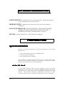
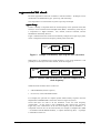
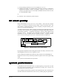
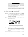
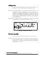
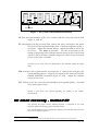
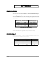
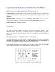
BIT CLOCK REGENERATION
PREPARATION................................................................................. 24
synchronization ......................................................................... 24
stolen bit clock .........................................................................................24
regenerated bit clock ................................................................................25
jitter..........................................................................................................26
BIT CLOCK REGEN module................................................... 26
procedure................................................................................... 27
bit clock quality......................................................................... 28
system performance................................................................... 28
EXPERIMENT ................................................................................... 29
bit clock recovery - method #1.................................................. 29
adding noise .............................................................................................30
bit clock ‘quality’ .....................................................................................30
bit clock recovery - method #2.................................................. 31
bit error rate............................................................................... 32
TUTORIAL QUESTIONS ................................................................. 33
APPENDIX......................................................................................... 34
digital delay ............................................................................... 34
divide-by-2 ................................................................................ 34
Bit clock regeneration
Vol D2, ch 3, rev 1.3
- 23
BIT CLOCK REGENERATION
ACHIEVEMENTS: introduction to bit clock regeneration. Evaluation using bitby-bit comparison with system bit clock.
PREREQUISITES: completion of at least some of the early experiments of
Volume D1.
ADVANCED MODULES: BIT CLOCK REGEN, LINE-CODE ENCODER,
ERROR COUNTING UTILITIES, INTEGRATE & DUMP. A
BASEBAND CHANNEL FILTERS module is optional.
TRUNKS: optional 208 kHz sine. Refer Laboratory Manager.
PREPARATION
synchronization
Receivers in a digital environment can require synchronization at at least three
different levels:
• carrier synchronization (in the case of bandpass signals)
• bit synchronization (at baseband)
• frame synchronization (at baseband)
This experiment is concerned with the second of these. It assumes either that the
signal has been transmitted at baseband, or successfully recovered from a higher
frequency carrier from which it has been demodulated.
stolen bit clock
For most TIMS experiments, when a bit clock is required by a receiver, it has been
convenient to use a ‘stolen’ clock. Bit clock regeneration from the received data
stream itself is not a trivial exercise, and is best avoided in the laboratory if at all
possible. This eliminates unnecessary complications, and sources of signal
corruption, and allows one to concentrate on other aspects of one`s investigations.
24 - D2
Bit clock regeneration
regenerated bit clock
Bit clock regeneration cannot be avoided in a real-life situation. Techniques can be
divided into two fundamental types: open loop, and closed loop.
This experiment is concerned with very basic open loop techniques.
open loop
If there is already a component at the bit clock frequency in the spectrum of the data
stream, it can be extracted with a bandpass filter (BPF). Alternatively, there may be
a component at a higher harmonic; this, instead, could be extracted, and the
fundamental obtained by division.
Figure 1 illustrates the basis of the most elementary example of an open loop system,
where a component at bit clock frequency already exists in the data.
incoming
data
BPF
sine
to
TTL
Figure 1: example of elementary open loop bit clock extraction
When there is no component at bit clock frequency or any of its harmonics it can
probably be created by a non-linear element, as shown in Figure 2.
incoming
bandlimited
data
non-linear
element
BPF
harmonic of
bit clock
PLL
DIVIDER
Figure 2: creation, and extraction, of a spectral component at bit
clock frequency
TIMS non-linear elements in this context are:
• a MULTIPLIER (used as a squarer)
• the CLIPPER, in the UTILITIES module
For example, the spectrum of a bipolar pseudo random binary sequence from the
SEQUENCE GENERATOR is of the form shown in Figure 3(a) below.
Notice that there are nulls at all the harmonics of the bit clock frequency
(2.0833 kHz). If this signal is first bandlimited, then squared, the spectrum,
Figure 3(b), now contains lines at the bit clock frequency and its harmonics. A
component at the bit rate can be extracted with, for example, a bandpass filter (BPF
– see the BIT CLOCK REGEN module), or a phase locked loop (PLL) – or perhaps
a combination of the two.
Bit clock regeneration
D2
- 25
(a)
(b)
Figure 3: PRBS signal spectrum (a) before and (b) after
bandlimiting and squaring
closed loop
Closed loop circuits use feedback. They make comparisons with received data and
expected data. They can involve the transmitter sending known sequences training sequences - which are used by the receiver to verify synchronization 1.
Closed loop systems are more accurate than open loop systems, but can be complex
and costly. They are outside the scope of present TIMS modules.
jitter
Bit clock recovery circuits can suffer from timing jitter.
Although the recovered clock is of the correct mean frequency, it can be undergoing
either or both of linear and non-linear modulation.
The effects of linear modulation can be removed (or at least reduced) by amplitude
limiting - by a comparator, for example.
The effects of non-linear modulation are not so easily overcome.
BIT CLOCK REGEN module
This is the first time the BIT CLOCK REGEN module
has been used. It is described in detail in the Advanced
Module User Manual.
As can be seen, from the drawing of the front panel
(opposite), the module contains four independent subsystems. These have been described separately in the
Chapter entitled Digital utility sub-systems (in this
Volume) to which you should refer.
DIVIDE BY n
TRANS. DET
LOOP FILTER
DUAL BPF
As its name implies, these sub-systems are useful in bit
clock regeneration schemes, examples of which are
given in the experiment to follow.
clk
You may also devise your own schemes.
1 recall the operation of the sliding window correlator for sequence alignment
26 - D2
Bit clock regeneration
procedure
Some of the signal formats available from the LINE-CODE ENCODER module can
be used to test bit clock recovery schemes.
There are only two examples of bit clock recovery scheme given in the experiment to
follow - one in detail, and the other in outline.
When completed, you are invited to investigate other methods of recovery in which
you are interested. In preparation, here are some reminders of signals and systems
which may be useful.
signal source
As already mentioned, the LINE-CODE ENCODER, driven by a SEQUENCE
GENERATOR at 2.084 kHz, is a good source of bit streams having different
characteristics. These serve as inputs to your bit clock regenerator, after passing
through a noisy, bandlimited channel.
modules
The following modules will be found useful in the work to follow:
•
•
BIT CLOCK REGEN module: not surprisingly, this module will be useful !
UTILITIES module: contains a CLIPPER/COMPARATOR - a useful odd-order
non-linear characteristic, and used for converting a sinewave to TTL format.
•
•
a MULTIPLIER, as a SQUARER, provides an even-order non-linear characteristic.
•
•
NOISE GENERATOR: a low SNR will put your regeneration system to the test.
VCO: as part of a phase locked loop (PLL). There is a loop filter in the BIT
CLOCK REGEN module, as well as a TTL divide-by-two sub-system.
the INSTRUMENTATION MODEL macro module will check BER
performance, although a simplified bit clock ‘quality’ arrangement is suggested.
bit clock component present ?
Before modelling a regeneration scheme, it might be a good idea to examine each of
the line codes to check whether it already has a bit clock component present in its
spectrum.
This can be done with the scheme of Figure 1.
bit clock component creation
For those spectra not already containing a spectral line at bit clock frequency try a
scheme as illustrated in Figure 2.
BIT CLOCK REGEN BPF
Using an internal clock, the BPF in the BIT CLK REGEN module may be tuned to
2.048 kHz.
It may be tuned to other frequencies by the use of an external sinusoid (eg, a VCO).
For example, to tune the BPF to 4.167 kHz (twice 2.048 kHz) requires a clock at
50 times this frequency, namely 208.33 kHz. This frequency may be obtained from:
1) a VCO:
a) by setting the on-board switch SW2 to FSK
b) toggling the front panel switch to HI
Bit clock regeneration
D2
- 27
c) leaving nothing connected to DATA IN (acceptable as a TTL LO)
d) adjusting RV7 (FSK1) for 208 kHz output (setting the frequency to 208 kHz by
watching the frequency counter is acceptable. However it may be easier to
connect a 4.167 kHz sine wave to the input of the BPF and then to tune the VCO
for a maximum BPF output).
or
2) TRUNKS. This would be the preferred option.
bit clock quality
Rather than measure bit error rate over a noisy channel - which tests the complete
system - it is instructive to measure just the ‘quality’ of the recovered bit clock. The
term ‘quality’ is used loosely here. It refers to frequency and phase stability, jitter,
and so on. See Tutorial Question Q5.
A method of measuring the quality consists of comparing the regenerated clock with
the system clock, using the X-OR in the ERROR COUNTING UTILITIES module, as
a performance indicator. A suggested arrangement is shown in block diagram form
in Figure 4 below. The phase of the sinusoidal output from the BPF is made
adjustable so it may be aligned with the reference bit clock. A digital VARIABLE
DELAY is inserted in the gate to the X-OR to control the instant of comparison.
LINE
CODE
PRBS
NOISY
BANDLIMITED
CHANNEL
PHASE
BIT REGEN
CIRCUITRY
A
X - OR
errors
B gate
TTL
DIGITAL DELAY
BIT CLOCK
Figure 4: measurement of bit clock quality
By appropriate adjustment of the analog phase and the TTL delay, and with no noise,
the arrangement can be set so as to register no errors.
Noise could then be added to the channel in order to make a more demanding test.
Reliable bit clock recovery should be possible for signal-to-noise ratios approaching
0 dB.
This system will be modelled in the experiment.
system performance
If the quality of the recovered bit clock is considered good, by the previous test, then
the overall system performance can be measured by carrying out a bit error rate
measurement over the noisy channel.
This is perhaps an unnecessary extension of the experiment, the aim of which was to
introduce some basic methods of bit clock recovery, without going into great detail.
28 - D2
Bit clock regeneration
EXPERIMENT
The complete system to be modelled involves many modules. It will be patched up
systematically. It is suggested that the modules be inserted into the TIMS frame in
the order shown, starting at the extreme left hand side.
In the first example a bit clock will be recovered from the UNI-RZ coded output
from the LINE-CODE ENCODER.
This waveform may be shown to contain energy at the bit clock frequency. So it can
be extracted with a BPF according to the scheme of Figure 1.
bit clock recovery - method #1
T1 acquire a BIT CLOCK REGEN module. Read about it in the Advanced
Modules User Manual. Before plugging it in locate the on-board
switch SW1. Set the left hand toggle UP and the right hand toggle
DOWN. This tunes BPF #1 to 2.083 kHz, and leaves BPF #2 to be
tuned by an external TTL signal (at 50 times the desired passband
frequency) later on in the experiment.
T2 patch up the diagram of Figure 5, which is a model of the open loop
regeneration scheme of Figure 1.
TTL bit
clock out
8.333 kHz MASTER
Figure 5: model of Figure 1
T3 using the 2.083 kHz as a reference on CH1-A, look at the output of BPF #1
with CH2-A. This will be a sinewave, also on a mean frequency of
2.083 kHz. However, its amplitude will be varying with time. Is this
due to amplitude modulation or phase modulation ? See Tutorial
Question Q1.
T4 observe the output of the COMPARATOR on CH2-B. This is a TTL signal, of
fixed amplitude, and mean frequency 2.083 kHz. Is its phase
varying ?
Bit clock regeneration
D2
- 29
adding noise
The above procedures demonstrated carrier regeneration from a wideband, noisefree signal. Now pass the test signal through a noisy, bandlimited channel.
T5 add a noisy, bandlimited channel 2 to the model, as in Figure 6 below. Use a
TUNEABLE LPF as the bandlimiting filter, or channel #3 of a
BASEBAND CHANNEL FILTERS module. Without noise, adjust the
gains of the TUNEABLE LPF (bandwidth set to maximum) and each
ADDER to unity. Include the PHASE SHIFTER; it will be required
later. Confirm the regenerated carrier is still present at the output of
the COMPARATOR.
T6 add noise. Estimate at what level of SNR the recovered bit clock might
become unusable ? Explain how you made this estimate.
TTL bit
clock out
8.333 kHz MASTER
Figure 6: adding a noisy channel
bit clock ‘quality’
Now add some instrumentation to measure the ‘quality’ of the recovered clock.
T7 add the error counting facility shown in Figure 7 below. This is based on the
scheme illustrated in Figure 4. As shown, the regenerated bit clock is
patched to the ‘A’ input f the X-OR gate, and the reference (the system
bit clock) into the ‘B’ input.
2 described in the experiment entitled The noisy channel model in Volume D1.
30 - D2
Bit clock regeneration
COUNTER GATE
ERROR COUNTER
8.333 kHz MASTER
Figure 7: the system with instrumentation added
T8 first check performance of the error counter with the system bit clock in both
inputs ‘A’ and ‘B’.
T9 when happy with the previous Task, remove the noise, and replace the stolen
bit clock with the regenerated bit clock. Check the alignment of the XOR inputs. Adjust the DIGITAL DELAY. Adjust the DIGITAL DELAY for
no errors 3. This must be possible ! For the record observe the
timing of the gating pulse from the DIGITAL DELAY to the X-OR clk with
respect to the X-OR inputs (and the range over which it may be moved
for no errors to be recorded).
Describe in your notes what you understand by the statement ‘adjust the digital
delay’.
T10 now patch the regenerated bit clock into the ‘A’ input of the X-OR gate (not
via the DIGITAL DELAY). Align the two inputs to the X-OR gate with the
PHASE SHIFTER (on-board switch set LO). Adjust the DIGITAL
DELAY for no errors.
T11 with no errors the recovered clock should be of acceptable quality. Now add
noise, and report results.
Record in your notes your opinion regarding the validity of the ‘quality’
measurements.
bit clock recovery - method #2
The previous bit clock recovery method extracted a component at bit clock
frequency which was already present in the data stream.
This second method is truly a regenerative method, since the data stream will not
have such a component present.
3 for details of range setting of the DIGITAL DELAY see the Appendix to this experiment.
Bit clock regeneration
D2
- 31
It will model the block diagram of Figure 2, using a MULTIPLIER as a squarer.
The model is shown in Figure 8 below. It is complete with recovered bit clock
‘quality’ assessment instrumentation.
Detailed step-by-step Tasks are not provided.
COUNTER INPUT
COUNTER GATE
8.333 kHz
MASTER
Figure 8: the TIMS model
You will note that the model contains 13 plugin modules (there are five within the
CHANNEL MODEL macro module - but one, the VARIABLE DC, is a fixed
module so does not require a free slot). These 13 cannot be accommodated within a
single TIMS 301 system.
However, if you use a QUADRATURE UTILITIES module which contains two
MULTIPIERS, then there is sufficient space in a single TIMS 301.
The BPF in the BIT CLOCK REGEN module must be tuned to 2.083 kHz by setting
the on-board switch SW1 to INT CLK.
The second MULTIPLIER, together with the VCO and LOOP FILTER in the BIT
CLOCK REGEN module, implements a phase locked loop (PLL). You might query
the need for this, since the output of the BPF is already a sinusoid at this frequency
(the sinusoid could be converted to TTL, as required by the EXCLUSIVE-OR gate in
the ERROR COUNTING UTILITIES, with the COMPARATOR in the UTILITIES
module). Consider the merits of both systems, and try each as time permits.
bit error rate
A final check of the quality of any bit clock recovery scheme would consist of
measuring the bit error rate of the overall system under different conditions.
TIMS can do that, following the procedures set out in the experiment entitled BER
measurement in the noisy channel (in this Volume). It would call for a second TIMS
301, or a TIMS Junior, to accommodate the extra modules.
It would also go beyond the intended aim of the experiment, which was to introduce
some elementary schemes of bit clock recovery.
32 - D2
Bit clock regeneration
TUTORIAL QUESTIONS
Q1 a bit clock, recovered as a sine wave with varying amplitude, may or may not
have uniform zero crossings. Give examples of the two cases. Which
one gives rise to timing jitter ?
Q2 how would the presence of timing jitter (in your extracted clock) show up on
the oscilloscope ?
Q3 can you distinguish, using only the oscilloscope, the difference between
amplitude jitter and phase jitter on a regenerated clock bit ?
Q4 what factors might influence the choice between an open loop and a closed
loop bit clock regeneration scheme ?
Q5 describe the various imperfections from which a recovered bit clock can
suffer.
Bit clock regeneration
D2
- 33
APPENDIX
digital delay
The DIGITAL DELAY sub-system is built into the INTEGRATE & DUMP module. It
is described in the Advanced Modules User Manual, as well as in the Chapter
entitled Digital utility sub-systems of this Volume.
The delay is adjustable by a front panel control DELAY, in conjunction with a toggle
switch SW3 mounted on the circuit board. The delays to be expected are shown in
the table below.
SW3-upper toggle
SW3-lower toggle
delay range from front
panel, using DELAY
RIGHT
RIGHT
10 µsec - 100 µsec
RIGHT
LEFT
60 µsec - 500 µsec
LEFT
RIGHT
100 µsec - 1 msec
LEFT
LEFT
150 µsec - 1.500 msec
on-board switch SW3 settings
The bit clock in the present experiment is 2 kHz, so the period is 500 µs.
divide-by-2
There is a TTL divide-by 1, 2, 4, or 8 in the BIT CLOCK REGEN module. The onboard switch setting s are shown in the Table below.
SW2-A (left)
SW2-B (right)
divide by
DOWN
DOWN
8
DOWN
UP
4
UP
DOWN
2
UP
UP
-1
on-board switch selectable division ratios
34 - D2
Bit clock regeneration