1
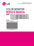
MODEL: L180p(9180-HB9)
COLOR MONITOR
SERVICE MANUAL
Chassis No. : CL-42
CAUTION
BEFORE SERVICING THE UNIT,
READ THE SAFETY PRECAUTIONS
IN THIS MANUAL.
CONTENTS
SPECIFICATIONS ................................................... 2
PRECAUTIONS ....................................................... 3
TIMING CHART ....................................................... 4
OPERATING INSTRUCTIONS ................................ 5
WIRING DIAGRAM ................................................. 6
BLOCK DIAGRAM ................................................... 7
DESCRIPTION OF BLOCK DIAGRAM.....................8
ADJUSTMENT ...................................................... 10
TROUBLESHOOTING GUIDE .............................. 12
EXPLODED VIEW...................................................16
EXPLODED VIEW PARTS LIST..............................17
REPLACEMENT PARTS LIST ...............................18
PIN CONFIGURATION............................................21
SCHEMATIC DIAGRAM ......................................... 23
SPECIFICATIONS
1. LCD CHARACTERISTICS
Type
: TFT SXGA LCD
Size
: 18.1inch(459.74mm)
Pixel Pitch
: 0.2805(H) x 0.2805(V)
Color Depth
: 8-bit, 16,777,216 colors
Electrical Interface
: LVDS
Surface Treatment
: Anti-Glare, Hard Coating (3H)
Operating Mode
: Normally Black
Backlight Unit
: Six-CCFL (Cold Cathode
Fluorescent Lamp)
2. OPTICAL CHARACTERISTICS
2-1. Viewing Angle by Contrast Ratio
Left
: -60° min., -85°(typ)
Right : +60° min., +85°(typ)
Top
: +60° min., +85°(typ)
Bottom : -60° min., -85°(typ)
≥ 10
2-2. Luminance
: 200(min), 250(typ)
2-3. Contrast Ratio
: 250(min), 400(typ)
4. POWER SUPPLY
4-1. Power Adaptor
Input
: AC 90~240V, 50/60 ±3Hz , 1.0A
4-2. Power Consumption
POWER ON (MAX)
ON/ON
ACTIVE
less than 55 W
GREEN
ACITIVE OFF
OFF/OFF
OFF
less than 3 W
AMBER
POWER OFF
-
-
less than 3 W
OFF
5. ENVIRONMENT
5-1. Operating Temperature: 10°C~35°C (50°F~95°F)
(Ambient)
5-2. Relative Humidity
: 10%~80%
(Non-condensing)
5-3. MTBF
: 50,000 Hours(Min)
6. DIMENSIONS
W
3. SIGNAL (Refer to the Timing Chart)
3-1. Sync Signal
• Type
: Separate, Composite,
SOG (Sync On Green)
Digital
3-2. Video Input Signal
1) Type
2) Voltage Level
a) Color 0, 0
b) Color 7, 0
c) Color 15, 0
3) Input Impedance
3-3. Operating Frequency
Analog
Horizontal
Vertical
Digital
Horizontal
Vertical
H/V SYNC VIDEO POWER CONSUMPTION LED COLOR
MODE
Without Tilt/Swivel
Width
: 396.0 mm (15.59'')
Depth
: 71.1 mm ( 2.79'')
Height
: 330.5 mm (13.01'')
H
D
W
: R, G, B Analog
: 0~0.71 V
: 0 Vp-p
: 0.467 Vp-p
: 0.714 Vp-p
: 75 Ω
With Tilt/Swivel
Width
: 396.0 mm (15.59'')
Depth
: 259.0 mm (10.19'')
Height
: 349.7 mm (13.7'')
H
D
7. WEIGHT
Without Stand
With Stand
: 31 ~ 81kHz
: 55 ~ 75Hz
: 31 ~ 68kHz
: 55 ~ 75Hz
-2-
: 5.3kg (11.69 lbs)
: 7.7kg (16.98 lbs)
PRECAUTION
WARNING FOR THE SAFETY-RELATED COMPONENT.
WARNING
• There are some special components used in LCD
monitor that are important for safety. These parts are
marked on the schematic diagram and the
replacement parts list. It is essential that these critical
parts should be replaced with the manufacturer’s
specified parts to prevent electric shock, fire or other
hazard.
• Do not modify original design without obtaining written
permission from IBM or you will void the original parts
and labor guarantee.
TAKE CARE DURING HANDLING THE LCD MODULE
WITH BACKLIGHT UNIT.
• Must mount the module using mounting holes arranged
in four corners.
• Do not press on the panel, edge of the frame strongly
or electric shock as this will result in damage to the
screen.
• Do not scratch or press on the panel with any sharp
objects, such as pencil or pen as this may result in
damage to the panel.
• Protect the module from the ESD as it may damage the
electronic circuit (C-MOS).
• Make certain that treatment person’s body are
grounded through wrist band.
• Do not leave the module in high temperature and in
areas of high humidity for a long time.
• The module not be exposed to the direct sunlight.
• Avoid contact with water as it may a short circuit within
the module.
• If the surface of panel become dirty, please wipe it off
with a softmaterial. (Cleaning with a dirty or rough cloth
may damage the panel.)
CAUTION
Please use only a plastic screwdriver to protect yourself
from shock hazard during service operation.
-3-
BE CAREFUL ELECTRIC SHOCK !
• If you want to replace with the new backlight (CCFL) or
inverter circuit, must disconnect the AC adapter
because high voltage appears at inverter circuit about
650Vrms.
• Handle with care wires or connectors of the inverter
circuit. If the wires are pressed cause short and may
burn or take fire.
TIMING CHART
VIDEO
B
A
E
C
D
SYNC
F
<< Dot Clock (MHz), Horizontal Frequency (kHz), Vertical Frequency (Hz), Horizontal etc... (µs), Vertical etc... (ms) >>
Mode
1
2
3
4
5
6
7
8
9
10
11
12
13
H/V
Sort
Sync
Polarity
H
+
V
–
H
–
V
H
+
–
V
–
H
–
V
H
–
+
V
+
H
+
V
+
H
+/–
V
+/–
H
–
V
–
H
–
V
–
H
+/–
V
+/–
H
+/–
V
+/–
H
+
V
+
H
+
V
+
Dot
Clock
25.175
28.321
25.175
31.5
40.0
49.5
57.283
65.0
78.75
100.0
92.978
108.0
135.0
Frequency
Total Period Video Active Time
(E)
(A)
Front Porch
(C)
Sync Duration
(D)
Back Porch
(F)
31.469
800
640
16
96
48
70.09
449
350
37
2
60
31.468
900
720
18
108
54
70.08
31.469
449
800
400
640
12
16
2
96
35
48
59.94
525
480
10
2
33
37.5
840
640
16
64
120
75
37.879
500
1056
480
800
1
40
3
128
16
88
60.317
628
600
1
4
23
46.875
1056
800
16
80
160
75.0
625
600
1
3
21
49.725
1152
832
32
64
224
74.55
667
624
1
3
39
48.363
1344
1024
24
136
160
60.0
806
768
3
6
29
60.123
1312
1024
16
96
176
75.029
800
768
1
3
28
68.681
1456
1152
64
128
144
75.062
915
870
1
3
39
61.805
1504
1152
18
134
200
65.96
937
900
2
4
31
63.981
1688
1280
48
112
248
60.02
1066
1024
1
3
38
79.976
1688
1280
16
144
248
75.035
1066
1024
1
3
38
-4-
Resolution
640x350
70Hz
720x400
70Hz
640x480
60Hz
640x480
75Hz
800x600
60Hz
800x600
75Hz
832x624
75Hz
1024x768
60Hz
1024x768
75Hz
1152x870
75Hz
1152x900
65Hz
1280x1024
60Hz
1280x1024
75Hz
OPERATING INSTRUCTIONS
FRONT VIEW
REAR VIEW
Power
Connect
AUDIO
DC OUT
Front Control Panel
Front Control Panel
USER CONTROL FEATURES
Icon
and
Monitor controls
Icon
Direct Access Functions
Switches the monitors on and off.
Bring up Brightness adjustment.
Display main OSD menu and selects
highlighted menu item.
Executes automatic image setup.
CONTROLS LOCK / UNLOCK
Moved the cursor to highlight icons or
make adjustments.
This feature allows you to secure the
current control settings, while allowing the
user to adjust Brightness, so that they
cannot be inadvertently changed. Push
and hold the enter button[ ] for 10
seconds; the message “Menu is Locked”
appears.
You can unlock the OSD controls at any
time by pushing the enter button[ ] for 10
seconds; the message “Menu is Unlocked”
will appear.
Exits from current OSD menu.
Switch between input signals.
-5-
WIRING DIAGRAM
Connector Ass’y P/N: 6631T11016D
Connector Ass’y P/N: 6631T20022E
J702
J705
-6-
-7-
AC Input
Power
12V
2.5V
5V
2.5V
Reg.
3.3V
Reg.
3.3V
5V
5V
12V
D-SUB
Inverter
3.3V
2.5V
Digital Signal or
Analog R,G,B,H/V
(ADC/LVDS/SCALER
/INPUT SWITCHING
/TMDS )
R,G,B, H/V Sync
12V
LVDS
(Low Voltage
Differential
Signaling)
MST9151B
including
R,G,B
differential
Inverter Output
LCD Module
DVI-I
MTV412
Micom
BLOCK DIAGRAM
DESCRIPTION OF BLOCK DIAGRAM
1. Video Controller Part & Display Data Transmitter Part.(MST9151B)
This part amplifies the level of video signal for the digital conversion and
converts from the analog video signal to the digital video signal using a pixel clock.
The pixel clock for each mode is generated by the PLL.
The range of the pixel clock is from 25MHz to 135MHz.
This part consists of the Scaler.
The Scaler gets the video signal converted analog to digital,
interpolates input to 1280 x 1024 resolution signal and outputs 8-bit R, G, B signal to transmitter.
Especially pre-amp / ADC / Video controller/ Transmitter are merged to one chip"MST9151B" by MSTAR.
This part transmit digital signal from the Scaler to the receiver of module.
2. Micom Part
This Part consists of EEPROM IC which stores control data, Reset IC and the Micom.
The Micom distinguishes polarity and frequency of the H/V Sync are supplied from signal cable.
The controlled data of each modes is stored in EEPROM.
3. Power Part
This part consists of the one 3.3V and one 2.5 regulators to convert power which is provided 5V in LIPS Board.
Also, 5V is converted 3.3V and 2.5V by regulator. Converted power is provided for Scaler IC in the main board.
12V is provided for LCD Panel.
4. Inverter
The inverter converts from DC12V to AC 700Vrms and operates back-light lamps of module.
-8-
12V
50 ~ 60Hz
EMI
COMPONENTS
INPUT RECTIFIER
AND FILTER
HVDC
ENERGY
TRANSFER
100KHz
OUTPUT RECTIFIER
AND FILTER
5V
GND
LINE
100 ~ 240V
PWM CONTROL
CIRCUIT
PRIMARY
12V
SIGNAL
COLLECTION
PHOTO-COUPLER
ISOLATION
SECONDARY
INVERTER CIRCUIT
High Voltage output
Operation description_Power
1. EMI components.
This part contains of EMI components to comply with global marketing EMI standards like FCC, VCCI CISPR, the
circuit included a line-filter, across line capacitor and of course the primary protection fuse.
2. Input rectifier and filter.
This part function is for transfer the input AC voltage to a DC voltage through a bridge rectifier and a bulk capacitor.
3. Energy Transfer.
This part function is transfer the primary energy to secondary through a power transformer.
4. Output rectifier and filter.
This part function is to make a pulse width modulation control and to provide the driver signal to power switch, to
adjust the duty cycle during different AC input and output loading condition to achive the dc output stablize, and also
the over power protection is also monitor by this part.
5. Photo-Coupler isolation.
This part function is to feed back the dc output changing status through a photo transistor to primary controller to
achieve the stabilized dc output voltage.
6. Signal collection.
This part function is to collect the any change from the dc output and feed back to the primary through photo
transistor
-9-
ADJUSTMENT
Windows EDID V1.0 User Manual
2. EDID Read & Write
1) Run WinEDID.exe
Operating System: MS Windows 98, 2000, XP
Port Setup: Windows 98 => Don’t need setup
Windows 2000, XP => Need to Port Setup.
This program is available to LCD Monitor only.
1. Port Setup
a) Copy “UserPort.sys” file to
“c:\WINNT\system32\drivers” folder
b) Run Userport.exe
2) Edit Week of Manufacture, Year of Manufacture,
Serial Number
a) Input User Info Data
b) Click “Update” button
c) Click “ Write” button
c) Remove all default number
d) Add 300-3FF
e) Click Start button.
f) Click Exit button.
- 10 -
SERVICE OSD
1) Turn off the power switch at the front side of the display.
2) Wait for about 3 seconds and press Source POWER switch with 1 second interval.
3) The SVC OSD menu contains additional menus that the User OSD menu as described below.
a) NVRAM INIT : EEPROM initialize(24C08)
b) ADC OFFSET : The lowest value of input leves sets to digitally 0(zero).
c) ADC GAIN : The highest value of input levels sets to digitally 255.
d) ADC CAL : W/B balance sets the gain and offset value.
e) ELAPSED CLEAR : To initialize using time.
f) AGING : To select factory aging mode.
g) ELAPSED TIME : ## Hr => Display the monitor's elapsed time.
A
9
IBM
Compatible PC
15
10
5
11
6
1
6
1
5
C
d
PARALLEL PORT
RS
EL
OFF
14
ON
LL
F
RA
PA
Power inlet (required)
5V
R
220
WE
VG
CS
T
MO
NI
Power Select Switch
(110V/220V)
Power LED
ON
TO
R
4.7K
OFF
74LS06
B
E ST Switch
B
F V-Sync On/Off Switch
(Switch must be ON.)
Figure 1. Cable Connection
- 11 -
4.7K
4.7K
5V
E
YN
A
PO
S
V-S
Control Line
5V
C
1
25
23
No
2C
tu
se
13
74LS06
TROUBLESHOOTING GUIDE
1. NO POWER
NO POWER
(POWER INDICATOR OFF)
CHECK J705
VOLTAGE
PIN6, PIN7 (5V)?
NO
CHECK POWER
BOARD, AND FIND
OUT A SHORT POINT
AS OPENING
EACH POWER LINE
YES
CHECK
U803 PIN 3
VOLTAGE
(5V) ?
NO
CHECK U803.
YES
CHECK
U804 PIN 3 Voltage
(5V) ?
NO
NO PROBLEM
YES
CHECK KEY CONTROL
CONNECTOR ROUTINE
IS U201
PIN114 (3.3V)
VOLTAGE REPEATED
AS PULSE
SHAPE ?
NO
YES
CHECK IIC LINE
CONNECTION
(U501, U502)
CHECK 5VS LINE
(OPEN CHECK)
CHECK U201 VCC,
- 12 -
2. NO RASTER (OSD IS NOT DISPLAYED) – LIPS
NO RASTER
(OSD IS NOT DISPLAYED)
J705
PIN 6, PIN 7
5V?
NO
CHECK LIPS
YES
J705 PIN 12
12V?
NO
CHECK LIPS
YES
J705 PIN1
5PWM,0V?
NO
CHECK U201 PIN45
PWM PORT
YES
CHECK
PULSE AS
CONTACTING SCOPE
PROBE TO CAUTION LABEL.
(CONTACT PROBE TO
CAUTION LABEL.
CAN YOU SEE PULSE
AT YOUR
SCOPE?
NO
YES
REPLACE CCFL LAMP
IN THE LCD MODULE
- 13 -
LIPS
3. NO RASTER (OSD IS NOT DISPLAYED) – MST9151
NO RASTER
(OSD IS NOT DISPLAYED)
U201
POWER PINS
3.3V?
NO
CHECK U804
YES
U201
PIN122, 123
OSCILLATE AS
12MHZ?
NO
1. CHECK PIN122, 123
SOLDERING CONDITION
2. CHECK X501
3. TROUBLE IN U201
YES
U501
PIN41 IS 64KHz H-SYNC?
PIN42 IS 60Hz V-SYNC?
IS PULSE APPEARED
AT SIGNAL PINS?
NO
YES
TROUBLE IN CABLE
OR LCD MODULE
- 14 -
CHECK CONNECTION LINE
FROM U201 TO U501
4. TROUBLE IN DPM
TROUBLE IN DPM
CHECK
R734, R741
(SYNC) ?
NO
CHECK PC
PC IS NOT GOING
INTO DPM OFF MODE
YES
CHECK
U501 PIN 11, 12
WAVEFORM
(12MHz) ?
NO
TROUBLE IN
X501
NO
TROUBLE IN
SIGNAL CABLE
YES
CHECK
U501 PIN 24
(0V) ?
YES
TROUBLE IN PC
- 15 -
EXPLODED VIEW
12
12
a
a
15
3
b
10
14
10
11
c
9
8
7
4
2
13
1
6
5
- 16 -
EXPLODED VIEW PARTS LIST
Ref. No.
Part No.
1
3091TKL102A
CABINET ASSEMBLY, LL180PL IBM L087 THINKVISION
2
6304FLP093A
LCD(LIQUID CRYSTAL DISPLAY), LM181E06-D4 LG PHILPS TFT COLOR TCO03,SXGA LVDS SMM
3
3809TKL074A
BACK COVER ASSEMBLY, LL180PL L070 THINKVISION
4
3043TKK050Y
TILT SWIVEL ASSEMBLY, LL180PL . STEALTH BLACK
5
6871TST458A
PWB(PCB) ASSEMBLY, SUB, L180P CONTROL TOTAL IBM AALDG
6
4810TKK221B
BRACKET, CONTROL PCB(LL180PL)
7
6631T11016D
CONNECTOR ASSEMBLY, 30P H-H 200MM UL20276 18" STD LG808H
8
6871TPT261B
PWB(PCB) ASSEMBLY, POWER, L180P POWER TOTAL SSE IBM18.1" FOR LPL
9
6871TMT492A
PWB(PCB) ASSEMBLY, MAIN, L180P ALRDG IBM CL-42 TOTAL
10
4814TKK264A
SHIELD, INVERTER LL180PL SHIELD
11
4951TKK162A
METAL ASSEMBLY, FRAME MAIN ASSY LL180PL
12
5040TKM064A
SCREW COVER(LL180PL)
13
4970TKK007A
SPRING, CLIP NO DIM FOR STAND CLIP(LI)
14
6850TD9001D
CABLE, D-SUB, UL 2990-9C(7.5) DT 3000MM STEALTH BK IBM DM
15
6866TDV004E
CABLE, DVI, UL20276 DT 3000MM STEALTH BK LI562G DM
a
1SZZTER001G
SCREW, DRAWING, D3.0 L6.0 MSWR/BK .
b
332-113S
SCREW, DRAWING D3.0 L12.0 MSWR/BK
C
1MCC0402416
SCREW MACHINE,COUNTER SUNK HEAD
Description
- 17 -
REPLACEMENT PARTS LIST
CAUTION: BEFORE REPLACING ANY OF THESE COMPONENTS,
READ CAREFULLY THE SAFETY PRECAUTIONS IN THIS MANUAL.
* NOTE : S SAFETY Mark
AL ALTERNATIVE PARTS
*S *AL LOC. NO.
PART NO.
DATE: 2003. 12. 12.
DESCRIPTION / SPECIFICATION
*S *AL LOC. NO.
MAIN BOARD
CAPACITORS
C204
C205
C206
C207
C208
C209
C210
C214
C215
C216
C217
C218
C219
C220
C221
C222
C223
C224
C225
C226
C227
C230
C231
C232
C233
C240
C244
C245
C246
C247
C248
C249
C250
C501
C502
C503
C505
C506
C507
C508
C509
C512
C513
C514
C516
C530
C703
C704
C705
C706
C707
C708
0CK104CK56A
0CK104CK56A
0CK104CK56A
0CK104CK56A
0CK104CK56A
0CK104CK56A
0CK104CK56A
0CK104CK56A
0CK104CK56A
0CK104CK56A
0CK104CK56A
0CK104CK56A
0CK104CK56A
0CK104CK56A
0CK104CK56A
0CK104CK56A
0CK104CK56A
0CK104CK56A
0CK104CK56A
0CK104CK56A
0CK104CK56A
0CK104CK56A
0CK104CK56A
0CK104CK56A
0CK104CK56A
0CK104CK56A
0CK104CK56A
0CK104CK56A
0CK104CK56A
0CK104CK56A
0CK104CK56A
0CK104CK56A
0CK104CK56A
0CK104CK56A
0CC101CK41A
0CC101CK41A
0CC101CK41A
0CC101CK41A
0CK104CK56A
0CC101CK41A
0CC101CK41A
0CC180CK41A
0CC030CK01A
0CH8106F611
0CK104CK56A
0CK103CK51A
0CK104CK56A
0CC101CK41A
0CC680CK41A
0CC680CK41A
0CC680CK41A
0CK103CK51A
C709
C710
C711
C712
C713
C714
C730
C731
C732
C734
C735
C737
C738
C739
C740
C741
C742
C743
C744
C750
C751
C752
C760
C801
C802
C803
C804
C817
C818
C819
C820
C821
C822
C828
C829
C831
C832
0.1UF 1608 50V 10% R/TP X7R
0.1UF 1608 50V 10% R/TP X7R
0.1UF 1608 50V 10% R/TP X7R
0.1UF 1608 50V 10% R/TP X7R
0.1UF 1608 50V 10% R/TP X7R
0.1UF 1608 50V 10% R/TP X7R
0.1UF 1608 50V 10% R/TP X7R
0.1UF 1608 50V 10% R/TP X7R
0.1UF 1608 50V 10% R/TP X7R
0.1UF 1608 50V 10% R/TP X7R
0.1UF 1608 50V 10% R/TP X7R
0.1UF 1608 50V 10% R/TP X7R
0.1UF 1608 50V 10% R/TP X7R
0.1UF 1608 50V 10% R/TP X7R
0.1UF 1608 50V 10% R/TP X7R
0.1UF 1608 50V 10% R/TP X7R
0.1UF 1608 50V 10% R/TP X7R
0.1UF 1608 50V 10% R/TP X7R
0.1UF 1608 50V 10% R/TP X7R
0.1UF 1608 50V 10% R/TP X7R
0.1UF 1608 50V 10% R/TP X7R
0.1UF 1608 50V 10% R/TP X7R
0.1UF 1608 50V 10% R/TP X7R
0.1UF 1608 50V 10% R/TP X7R
0.1UF 1608 50V 10% R/TP X7R
0.1UF 1608 50V 10% R/TP X7R
0.1UF 1608 50V 10% R/TP X7R
0.1UF 1608 50V 10% R/TP X7R
0.1UF 1608 50V 10% R/TP X7R
0.1UF 1608 50V 10% R/TP X7R
0.1UF 1608 50V 10% R/TP X7R
0.1UF 1608 50V 10% R/TP X7R
0.1UF 1608 50V 10% R/TP X7R
0.1UF 1608 50V 10% R/TP X7R
100PF 1608 50V 5% R/TP NP0
100PF 1608 50V 5% R/TP NP0
100PF 1608 50V 5% R/TP NP0
100PF 1608 50V 5% R/TP NP0
0.1UF 1608 50V 10% R/TP X7R
100PF 1608 50V 5% R/TP NP0
100PF 1608 50V 5% R/TP NP0
18PF 1608 50V 5% R/TP NP0
3PF 1608 50V 0.25 PF R/TP NP0
10UF 16V M 85STD(CYL) R/TP
0.1UF 1608 50V 10% R/TP X7R
0.01UF 1608 50V 10% R/TP B(Y5
0.1UF 1608 50V 10% R/TP X7R
100PF 1608 50V 5% R/TP NP0
68PF 1608 50V 5% R/TP NP0
68PF 1608 50V 5% R/TP NP0
68PF 1608 50V 5% R/TP NP0
0.01UF 1608 50V 10% R/TP B(Y5
PART NO.
DATE: 2003. 12. 12.
DESCRIPTION / SPECIFICATION
0CK103CK51A
0CK103CK51A
0CK103CK51A
0CK104CK56A
0CC101CK41A
0CC101CK41A
0CC101CK41A
0CC680CK41A
0CK103CK51A
0CK105CD56A
0CK105CD56A
0CK104CK56A
0CK104CK56A
0CK104CK56A
0CE477EH618
0CK104CK56A
0CK104CK56A
0CK104CK56A
0CK104CK56A
0CE477EH618
0CE477EH618
0CK103CK51A
0CE107EF610
0CK103CK51A
0CK104CK56A
0CK105CD56A
0CC102CK41A
0CE107EF610
0CK104CK56A
0CK103CK51A
0CE107EF610
0CK103CK51A
0CK104CK56A
0CK104CK56A
0CK103CK51A
0CE107EF610
0CE107EF610
0.01UF 1608 50V 10% R/TP B(Y5
0.01UF 1608 50V 10% R/TP B(Y5
0.01UF 1608 50V 10% R/TP B(Y5
0.1UF 1608 50V 10% R/TP X7R
100PF 1608 50V 5% R/TP NP0
100PF 1608 50V 5% R/TP NP0
100PF 1608 50V 5% R/TP NP0
68PF 1608 50V 5% R/TP NP0
0.01UF 1608 50V 10% R/TP B(Y5
1UF 1608 10V 10% R/TP X7R
1UF 1608 10V 10% R/TP X7R
0.1UF 1608 50V 10% R/TP X7R
0.1UF 1608 50V 10% R/TP X7R
0.1UF 1608 50V 10% R/TP X7R
470UF KMG 25V M FL TP 5
0.1UF 1608 50V 10% R/TP X7R
0.1UF 1608 50V 10% R/TP X7R
0.1UF 1608 50V 10% R/TP X7R
0.1UF 1608 50V 10% R/TP X7R
470UF KMG 25V M FL TP 5
470UF KMG 25V M FL TP 5
0.01UF 1608 50V 10% R/TP B(Y5
100UF KMG,RD 16V 20% FL BULK
0.01UF 1608 50V 10% R/TP B(Y5
0.1UF 1608 50V 10% R/TP X7R
1UF 1608 10V 10% R/TP X7R
1000PF 1608 50V 5% R/TP NP0
100UF KMG,RD 16V 20% FL BULK
0.1UF 1608 50V 10% R/TP X7R
0.01UF 1608 50V 10% R/TP B(Y5
100UF KMG,RD 16V 20% FL BULK
0.01UF 1608 50V 10% R/TP B(Y5
0.1UF 1608 50V 10% R/TP X7R
0.1UF 1608 50V 10% R/TP X7R
0.01UF 1608 50V 10% R/TP B(Y5
100UF KMG,RD 16V 20% FL BULK
100UF KMG,RD 16V 20% FL BULK
0DS226009AA
0DS226009AA
0DS226009AA
0DD184009AA
0DS226009AA
0DS226009AA
0DS226009AA
0DS226009AA
0DS226009AA
0DS226009AA
0DS226009AA
0DS226009AA
0DS226009AA
0DS226009AA
KDS226 TP KEC SOT-23 80V 300
KDS226 TP KEC SOT-23 80V 300
KDS226 TP KEC SOT-23 80V 300
KDS184 TP KEC - 85V - - - 300
KDS226 TP KEC SOT-23 80V 300
KDS226 TP KEC SOT-23 80V 300
KDS226 TP KEC SOT-23 80V 300
KDS226 TP KEC SOT-23 80V 300
KDS226 TP KEC SOT-23 80V 300
KDS226 TP KEC SOT-23 80V 300
KDS226 TP KEC SOT-23 80V 300
KDS226 TP KEC SOT-23 80V 300
KDS226 TP KEC SOT-23 80V 300
KDS226 TP KEC SOT-23 80V 300
DIODEs
D701
D702
D706
D707
D708
D709
D710
D711
D712
D713
D714
D715
D716
D717
- 18 -
*S *AL LOC. NO.
D718
D719
ZD701
ZD702
ZD703
ZD704
ZD705
ZD706
ZD707
ZD708
ZD709
ZD711
ZD712
ZD713
ZD714
ZD715
PART NO.
DATE: 2003. 12. 12.
DESCRIPTION / SPECIFICATION
0DS226009AA
0DD184009AA
0DZ560009DA
0DZ560009DA
0DZ560009DA
0DZ560009DA
0DZ560009DA
0DZ560009DA
0DZ560009DA
0DZ560009DA
0DZ560009DA
0DZ560009DA
0DZ560009DA
0DZ560009DA
0DZ560009DA
0DZ560009DA
KDS226 TP KEC SOT-23 80V 300
KDS184 TP KEC - 85V - - - 300
UDZ S 5.6B TP ROHM-K SOD323 2
UDZ S 5.6B TP ROHM-K SOD323 2
UDZ S 5.6B TP ROHM-K SOD323 2
UDZ S 5.6B TP ROHM-K SOD323 2
UDZ S 5.6B TP ROHM-K SOD323 2
UDZ S 5.6B TP ROHM-K SOD323 2
UDZ S 5.6B TP ROHM-K SOD323 2
UDZ S 5.6B TP ROHM-K SOD323 2
UDZ S 5.6B TP ROHM-K SOD323 2
UDZ S 5.6B TP ROHM-K SOD323 2
UDZ S 5.6B TP ROHM-K SOD323 2
UDZ S 5.6B TP ROHM-K SOD323 2
UDZ S 5.6B TP ROHM-K SOD323 2
UDZ S 5.6B TP ROHM-K SOD323 2
0IPRPM3010B
0IZZTSZ320A
0ISG240860B
0IPH740800H
0ICS240213A
0ICS240213A
0TFVI80036A
0IPMGNS001D
0IPMGNS001E
MST9151B DUAL DVI -I PARALLEL
MYSON 42P BK OTP LL180PL
M24C08W6 SGS-THOMSON 8SOP R/T
74F08D 14P,SOIC TP QUAD 2-INP
CAT24WC02J-TE13 8P SOP TP 2K
CAT24WC02J-TE13 8P SOP TP 2K
SI3861DV VISHAY R/TP TSOP-6 4
LM1117MPX-2.5 NATIONAL SEMICO
LM1117MPX-3.3 NATIONAL SEMICO
*S *AL LOC. NO.
R211
R212
R213
R214
R215
R216
R217
R220
R240
R501
R502
R503
R504
R505
R506
R507
R508
R509
R510
R511
R512
R514
R515
R516
R517
R518
R519
R521
R522
R523
R524
R525
R528
R529
R530
R531
R532
R533
R534
R535
R537
R541
R542
R543
R544
R545
R547
R548
R551
R552
R553
R554
R555
R556
R557
R558
R559
R561
R563
R564
R565
R580
ICs
U201
U501
U502
U503
U702
U703
U802
U803
U804
COILs & COREs
L750
L751
6210TCE001G
6210TCE001G
HH-1M3216-501 CERATEC 3216MM
HH-1M3216-501 CERATEC 3216MM
TRANSISTOR
Q502
Q503
Q504
Q505
Q506
Q507
Q508
Q509
Q701
Q702
Q703
Q704
Q705
Q706
Q707
0TR390409AE
0IKE704200H
0TR390409AE
0TR390409AE
0TR390409AE
0TR390409AE
0TR390409AE
0TR390409AE
0TR390409AE
0TR390409AE
0TR390609FA
0TR390609FA
0TR390409AE
0TR390409AE
0TR390409AE
FAIRCHILD KST3904(LGEMTF) TP
KIA7042AP TO-92 TP 4.2 VOLT.
FAIRCHILD KST3904(LGEMTF) TP
FAIRCHILD KST3904(LGEMTF) TP
FAIRCHILD KST3904(LGEMTF) TP
FAIRCHILD KST3904(LGEMTF) TP
FAIRCHILD KST3904(LGEMTF) TP
FAIRCHILD KST3904(LGEMTF) TP
FAIRCHILD KST3904(LGEMTF) TP
FAIRCHILD KST3904(LGEMTF) TP
KST3906-MTF TP SAMSUNG SOT23
KST3906-MTF TP SAMSUNG SOT23
FAIRCHILD KST3904(LGEMTF) TP
FAIRCHILD KST3904(LGEMTF) TP
FAIRCHILD KST3904(LGEMTF) TP
RESISTORs
R201
R202
R203
R205
R207
R208
R209
R210
0RJ0682D677
0RJ0682D677
0RJ0682D677
0RJ0000D677
0RJ3900D677
0RJ0682D677
0RJ0682D677
0RJ0682D677
68 OHM 1/10 W 5% 1608 R/TP
68 OHM 1/10 W 5% 1608 R/TP
68 OHM 1/10 W 5% 1608 R/TP
0 OHM 1/10 W 5% 1608 R/TP
390 OHM 1/10 W 5% 1608 R/TP
68 OHM 1/10 W 5% 1608 R/TP
68 OHM 1/10 W 5% 1608 R/TP
68 OHM 1/10 W 5% 1608 R/TP
- 19 -
PART NO.
0RJ0682D677
0RJ0682D677
0RJ0682D677
0RJ0682D677
0RJ0682D677
0RJ0682D677
0RJ0682D677
0RJ4701D677
0RJ0682D677
0RJ4701D677
0RJ4701D677
0RJ1000D677
0RJ4701D677
0RJ1000D677
0RJ1000D677
0RJ1000D677
0RJ1000D677
0RJ4701D677
0RJ4700D677
0RJ4700D677
0RJ4701D677
0RJ4701D677
0RJ1002D677
0RJ4701D677
0RJ4701D677
0RJ1000D677
0RJ1000D677
0RJ1000D677
0RJ1000D677
0RJ0332D677
0RJ0332D677
0RJ1002D677
0RJ1000D677
0RJ1000D677
0RJ1000D677
0RJ1000D677
0RJ3301D677
0RJ0332D677
0RJ0332D677
0RJ3301D677
0RJ4701D677
0RJ4701D677
0RJ1000D677
0RJ4701D677
0RJ4701D677
0RJ4701D677
0RJ4701D677
0RJ4701D677
0RJ4701D677
0RJ1001D677
0RJ4701D677
0RJ4701D677
0RJ4701D677
0RJ4701D677
0RJ1001D677
0RJ4701D677
0RJ1001D677
0RJ1000D677
0RJ1000D677
0RJ1000D677
0RJ4701D677
0RJ1001D677
DATE: 2003. 12. 12.
DESCRIPTION / SPECIFICATION
68 OHM 1/10 W 5% 1608 R/TP
68 OHM 1/10 W 5% 1608 R/TP
68 OHM 1/10 W 5% 1608 R/TP
68 OHM 1/10 W 5% 1608 R/TP
68 OHM 1/10 W 5% 1608 R/TP
68 OHM 1/10 W 5% 1608 R/TP
68 OHM 1/10 W 5% 1608 R/TP
4.7K OHM 1/10 W 5% 1608 R/TP
68 OHM 1/10 W 5% 1608 R/TP
4.7K OHM 1/10 W 5% 1608 R/TP
4.7K OHM 1/10 W 5% 1608 R/TP
100 OHM 1/10 W 5% 1608 R/TP
4.7K OHM 1/10 W 5% 1608 R/TP
100 OHM 1/10 W 5% 1608 R/TP
100 OHM 1/10 W 5% 1608 R/TP
100 OHM 1/10 W 5% 1608 R/TP
100 OHM 1/10 W 5% 1608 R/TP
4.7K OHM 1/10 W 5% 1608 R/TP
470 OHM 1/10 W 5% 1608 R/TP
470 OHM 1/10 W 5% 1608 R/TP
4.7K OHM 1/10 W 5% 1608 R/TP
4.7K OHM 1/10 W 5% 1608 R/TP
10K OHM 1/10 W 5% 1608 R/TP
4.7K OHM 1/10 W 5% 1608 R/TP
4.7K OHM 1/10 W 5% 1608 R/TP
100 OHM 1/10 W 5% 1608 R/TP
100 OHM 1/10 W 5% 1608 R/TP
100 OHM 1/10 W 5% 1608 R/TP
100 OHM 1/10 W 5% 1608 R/TP
33 OHM 1/10 W 5% 1608 R/TP
33 OHM 1/10 W 5% 1608 R/TP
10K OHM 1/10 W 5% 1608 R/TP
100 OHM 1/10 W 5% 1608 R/TP
100 OHM 1/10 W 5% 1608 R/TP
100 OHM 1/10 W 5% 1608 R/TP
100 OHM 1/10 W 5% 1608 R/TP
3.3K OHM 1/10 W 5% 1608 R/TP
33 OHM 1/10 W 5% 1608 R/TP
33 OHM 1/10 W 5% 1608 R/TP
3.3K OHM 1/10 W 5% 1608 R/TP
4.7K OHM 1/10 W 5% 1608 R/TP
4.7K OHM 1/10 W 5% 1608 R/TP
100 OHM 1/10 W 5% 1608 R/TP
4.7K OHM 1/10 W 5% 1608 R/TP
4.7K OHM 1/10 W 5% 1608 R/TP
4.7K OHM 1/10 W 5% 1608 R/TP
4.7K OHM 1/10 W 5% 1608 R/TP
4.7K OHM 1/10 W 5% 1608 R/TP
4.7K OHM 1/10 W 5% 1608 R/TP
1K OHM 1/10 W 5% 1608 R/TP
4.7K OHM 1/10 W 5% 1608 R/TP
4.7K OHM 1/10 W 5% 1608 R/TP
4.7K OHM 1/10 W 5% 1608 R/TP
4.7K OHM 1/10 W 5% 1608 R/TP
1K OHM 1/10 W 5% 1608 R/TP
4.7K OHM 1/10 W 5% 1608 R/TP
1K OHM 1/10 W 5% 1608 R/TP
100 OHM 1/10 W 5% 1608 R/TP
100 OHM 1/10 W 5% 1608 R/TP
100 OHM 1/10 W 5% 1608 R/TP
4.7K OHM 1/10 W 5% 1608 R/TP
1K OHM 1/10 W 5% 1608 R/TP
*S *AL LOC. NO.
R581
R590
R591
R592
R593
R595
R596
R701
R703
R705
R706
R707
R708
R709
R716
R717
R722
R723
R724
R725
R726
R727
R728
R729
R730
R731
R732
R733
R734
R735
R740
R741
R744
R745
R747
R748
R750
R751
R753
R754
R755
R756
R757
R758
R759
R761
R762
R763
R764
R765
R766
R767
R768
R769
R770
R771
R772
R773
R774
R775
R803
R811
PART NO.
0RJ1000D677
0RJ1000D677
0RJ1000D677
0RJ1000D677
0RJ1000D677
0RJ1000D677
0RJ4701D677
0RJ0752D677
0RJ0752D677
0RJ1000D677
0RJ0752D677
0RJ0272D677
0RJ4700D677
0RJ4700D677
0RJ4701D677
0RJ4701D677
0RJ1000D677
0RJ0332D677
0RJ0332D677
0RJ4701D677
0RJ1002D677
0RJ1002D677
0RJ0222D677
0RJ0222D677
0RJ1000D677
0RJ4700D677
0RJ4701D677
0RJ1001D677
0RJ4701D677
0RJ0000D677
0RJ1001D677
0RJ4701D677
0RJ4701D677
0RJ4701D677
0RJ4701D677
0RJ4701D677
0RJ0000D677
0RJ1002D677
0RJ1001D677
0RJ4701D677
0RJ4701D677
0RJ0272D677
0RJ4701D677
0RJ0752D677
0RJ0752D677
0RJ0752D677
0RJ4701D677
0RJ1002D677
0RJ1002D677
0RJ0332D677
0RJ0332D677
0RJ1001D677
0RJ1001D677
0RJ0122D677
0RJ0122D677
0RJ0122D677
0RJ0122D677
0RJ0122D677
0RJ0122D677
0RJ1002D677
0RJ0000D677
0RJ2202D677
DATE: 2003. 12. 12.
DESCRIPTION / SPECIFICATION
*S *AL LOC. NO.
100 OHM 1/10 W 5% 1608 R/TP
100 OHM 1/10 W 5% 1608 R/TP
100 OHM 1/10 W 5% 1608 R/TP
100 OHM 1/10 W 5% 1608 R/TP
100 OHM 1/10 W 5% 1608 R/TP
100 OHM 1/10 W 5% 1608 R/TP
4.7K OHM 1/10 W 5% 1608 R/TP
75 OHM 1/10 W 5% 1608 R/TP
75 OHM 1/10 W 5% 1608 R/TP
100 OHM 1/10 W 5% 1608 R/TP
75 OHM 1/10 W 5% 1608 R/TP
27 OHM 1/10 W 5% 1608 R/TP
470 OHM 1/10 W 5% 1608 R/TP
470 OHM 1/10 W 5% 1608 R/TP
4.7K OHM 1/10 W 5% 1608 R/TP
4.7K OHM 1/10 W 5% 1608 R/TP
100 OHM 1/10 W 5% 1608 R/TP
33 OHM 1/10 W 5% 1608 R/TP
33 OHM 1/10 W 5% 1608 R/TP
4.7K OHM 1/10 W 5% 1608 R/TP
10K OHM 1/10 W 5% 1608 R/TP
10K OHM 1/10 W 5% 1608 R/TP
22 OHM 1/10 W 5% 1608 R/TP
22 OHM 1/10 W 5% 1608 R/TP
100 OHM 1/10 W 5% 1608 R/TP
470 OHM 1/10 W 5% 1608 R/TP
4.7K OHM 1/10 W 5% 1608 R/TP
1K OHM 1/10 W 5% 1608 R/TP
4.7K OHM 1/10 W 5% 1608 R/TP
0 OHM 1/10 W 5% 1608 R/TP
1K OHM 1/10 W 5% 1608 R/TP
4.7K OHM 1/10 W 5% 1608 R/TP
4.7K OHM 1/10 W 5% 1608 R/TP
4.7K OHM 1/10 W 5% 1608 R/TP
4.7K OHM 1/10 W 5% 1608 R/TP
4.7K OHM 1/10 W 5% 1608 R/TP
0 OHM 1/10 W 5% 1608 R/TP
10K OHM 1/10 W 5% 1608 R/TP
1K OHM 1/10 W 5% 1608 R/TP
4.7K OHM 1/10 W 5% 1608 R/TP
4.7K OHM 1/10 W 5% 1608 R/TP
27 OHM 1/10 W 5% 1608 R/TP
4.7K OHM 1/10 W 5% 1608 R/TP
75 OHM 1/10 W 5% 1608 R/TP
75 OHM 1/10 W 5% 1608 R/TP
75 OHM 1/10 W 5% 1608 R/TP
4.7K OHM 1/10 W 5% 1608 R/TP
10K OHM 1/10 W 5% 1608 R/TP
10K OHM 1/10 W 5% 1608 R/TP
33 OHM 1/10 W 5% 1608 R/TP
33 OHM 1/10 W 5% 1608 R/TP
1K OHM 1/10 W 5% 1608 R/TP
1K OHM 1/10 W 5% 1608 R/TP
12 OHM 1/10 W 5% 1608 R/TP
12 OHM 1/10 W 5% 1608 R/TP
12 OHM 1/10 W 5% 1608 R/TP
12 OHM 1/10 W 5% 1608 R/TP
12 OHM 1/10 W 5% 1608 R/TP
12 OHM 1/10 W 5% 1608 R/TP
10K OHM 1/10 W 5% 1608 R/TP
0 OHM 1/10 W 5% 1608 R/TP
22K OHM 1/10 W 5% 1608 R/TP
R812
R814
R815
R840
R841
R842
R843
R844
R845
R846
R847
R848
R849
PART NO.
DATE: 2003. 12. 12.
DESCRIPTION / SPECIFICATION
0RJ5600D677
0RJ5600D677
0RJ0000D677
0RJ0332D677
0RJ0332D677
0RJ0332D677
0RJ0332D677
0RJ0332D677
0RJ0332D677
0RJ0332D677
0RJ0332D677
0RJ0332D677
0RJ0332D677
560 OHM 1/10 W 5% 1608 R/TP
560 OHM 1/10 W 5% 1608 R/TP
0 OHM 1/10 W 5% 1608 R/TP
33 OHM 1/10 W 5% 1608 R/TP
33 OHM 1/10 W 5% 1608 R/TP
33 OHM 1/10 W 5% 1608 R/TP
33 OHM 1/10 W 5% 1608 R/TP
33 OHM 1/10 W 5% 1608 R/TP
33 OHM 1/10 W 5% 1608 R/TP
33 OHM 1/10 W 5% 1608 R/TP
33 OHM 1/10 W 5% 1608 R/TP
33 OHM 1/10 W 5% 1608 R/TP
33 OHM 1/10 W 5% 1608 R/TP
6612TAH003A
6212AA2004A
DJ-023 KSD R/ANGLE LB563B
HC-49U TXC 12.0MHZ +/- 30 PPM
OTHERs
J708
X501
CONTROL BOARD
LED1
R1
R2
R3
R4
R5
SW1
SW2
SW3
SW4
SW5
ZD1
ZD2
- 20 -
0DLRH0058AA
0RJ4701D677
0RJ4701D677
0RJ8200D677
0RJ8200D677
0RJ1501D677
6600TR1002A
6600TR1002A
6600TR1002A
6600TR1002A
6600TR1002A
0DZ560009DA
0DZ560009DA
ROHM SML-521MYWT86 R/TP GREEN
4.7K OHM 1/10 W 5% 1608 R/TP
4.7K OHM 1/10 W 5% 1608 R/TP
820 OHM 1/10 W 5% 1608 R/TP
820 OHM 1/10 W 5% 1608 R/TP
1.5K OHM 1/10 W 5% 1608 R/TP
SKQGACE010 J-ALPS NON 12V 50M
SKQGACE010 J-ALPS NON 12V 50M
SKQGACE010 J-ALPS NON 12V 50M
SKQGACE010 J-ALPS NON 12V 50M
SKQGACE010 J-ALPS NON 12V 50M
UDZ S 5.6B TP ROHM-K SOD323 2
UDZ S 5.6B TP ROHM-K SOD323 2
PIN CONFIGURATION
MST9151 DUAL MSTAR 128P
HSYNC1
VSYNC0
HSYNC0
AVSS_PLL
AVDD_PLL
XOUT
XIN
HWRESETZ
DDCROM_DAT
DDCROM_CLK
DDC1_CLK
DDC1_DAT
DDC2_CLK
DDC2_DAT
VDDP
GNDP
GNDC
VDDC
NC
NC
NC
VDDP
GNDP
NC
NC
BYPASS
128
127
126
125
124
123
122
121
120
119
118
117
116
115
114
113
112
111
110
109
108
107
106
105
104
103
PIN DIAGRAM
VSYNC1
1
102
AVSS_PLL
AVSS_DVI
2
101
NC
R+
3
100
NC
R-
4
99
NC
AVSS_DVI
5
98
NC
G+
6
97
LVB0M
G-
7
96
LVB0P
AVDD_DVI
8
95
GNDP
B+
9
94
VDDP
B-
10
93
LVB1M
AVSS_DVI
11
92
LVB1P
CK+
12
91
LVB2M
Pin 1
90
LVB2P
14
89
LVBCKM
REXT
15
88
LVBCKP
AVDD_PLL
16
87
LVB3M
AVSS_PLL
17
86
LVB3P
AVDD
18
85
VDDC
AVSS
19
84
GNDC
BIN1
20
83
GNDP
BIN1M
21
82
VDDP
SOGIN1
22
81
LVA0M
GIN1
23
80
LVA0P
GIN1M
24
79
LVA1M
RIN1
25
78
LVA1P
RIN1M
26
77
LVA2M
BIN0M
27
76
LVA2P
BIN0
28
75
LVACKM
GIN0M
29
74
LVACKP
GIN0
30
73
GNDP
SOGIN0
31
72
VDDP
RIN0M
32
71
LVA3M
RIN0
33
70
LVA3P
AVSS
34
69
NC
AVDD
35
68
NC
VC646960210F
13
MST9151
CKAVDD_DVI
- 21 -
62
63
64
GNDP
GNDC
VDDC
59
NC
61
58
VDDC
60
57
GNDC
NC
56
VDDP
55
VDDP
GNDP
50
NC
54
49
NC
NC
48
NC
53
47
NC
NC
46
NC
52
45
PWM1
NC
44
PWM0
51
43
INT
NC
42
NC
41
65
SCL
38
SDA
NC
REFM
CSZ
NC
66
40
67
37
39
36
AVSS
RMID
REFP
CAT24WC08J-TE13 8P
BLOCK DIAGRAM
DIP Package(p)
SOIX Package(J)
EXTERNAL LOAD
A0
1
8
1
8
2
7
VCC
WP
A0
A1
A1
2
7
VCC
WP
A2
3
6
SCL
A2
3
6
SCL
V SS
4
5
SDA
V SS
4
5
SDA
SENSE AMPS
SHIFT REGISTERS
D OUT
ACK
V CC
V SS
COLUMN
DECODERS
WORD ADDRESS
BUFFERS
TSSOP Package(U)
SDA
A0
1
8
A1
2
7
A2
V SS
3
6
SCL
4
5
SDA
START/STOP
LOGIC
VCC
WP
XDEC
WP
E 2 PROM
CONTROL
LOGIC
PIN CONFIGURATION
PIN FUNCTION
DATA IN STORAGE
Pin Name
Function
A0, A1, A2
Device Adress Inputs
SDA
Serial Data/Address
SCL
Serial Clock
WP
Write Protect
Vcc
+1.8V to + 6.0V power Supply
Vss
Ground
HIGH VOLTAGE/
TIMING CONTROL
SCL
A0
A1
A2
- 22 -
STATE COUNTERS
SLAVE
ADDRESS
COMPARATORS
SCHEMATIC DIAGRAM
1. SCALER
- 23 -
2. MICOM
- 24 -
3. POWER
- 25 -
4. CONNECTOR & JACKS
- 26 -
5. CONTROL KEY
- 27 -
Feb. 2004
Printed in Korea
P/NO : 3828TSO049G