1
website:http://biz.LGservice.com
e-mail:http://www.LGEservice.com/techsup.html
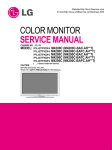
CHASSIS : ML-041B
jel
MODEL: RM-15LA70C
.ne
t
LCD TV
SERVICE MANUAL
.w
CAUTION
//w
ww
BEFORE SERVICING THE CHASSIS,
READ THE SAFETY PRECAUTIONS IN THIS MANUAL.
htt
p:
R
CONTENTS
CONTENTS .............................................................................................. 2
PRODUCT SAFETY ..................................................................................3
t
SPECIFICATION ........................................................................................4
.ne
TIMING CHART........................................................................................11
jel
ADJUSTMENT INSTRUCTION ...............................................................12
TROUBLE SHOOTING ............................................................................16
.w
BLOCK DIAGRAM...................................................................................21
ww
WIRING DIAGRAM ..................................................................................23
EXPLODED VIEW .................................................................................. 24
//w
EXPLODED VIEW PARTS LIST ..............................................................25
REPLACEMENT PARTS LIST ............................................................... 26
htt
p:
SVC. SHEET ...............................................................................................
-2-
SAFETY PRECAUTIONS
IMPORTANT SAFETY NOTICE
Many electrical and mechanical parts in this chassis have special safety-related characteristics. These parts are identified by
in the
Schematic Diagram and Replacement Parts List.
It is essential that these special safety parts should be replaced with the same components as recommended in this manual to prevent
X-RADIATION, Shock, Fire, or other Hazards.
Do not modify the original design without permission of manufacturer.
Before returning the receiver to the customer,
An isolation Transformer should always be used during the
servicing of a receiver whose chassis is not isolated from the AC
power line. Use a transformer of adequate power rating as this
protects the technician from accidents resulting in personal injury
from electrical shocks.
always perform an AC leakage current check on the exposed
metallic parts of the cabinet, such as antennas, terminals, etc., to
be sure the set is safe to operate without damage of electrical
shock.
.ne
t
General Guidance
Leakage Current Cold Check(Antenna Cold Check)
ww
Keep wires away from high voltage or high temperature parts.
.w
If any fuse (or Fusible Resistor) in this TV receiver is blown,
replace it with the specified.
When replacing a high wattage resistor (Oxide Metal Film Resistor,
over 1W), keep the resistor 10mm away from PCB.
With the instrument AC plug removed from AC source, connect an
electrical jumper across the two AC plug prongs. Place the AC
switch in the on position, connect one lead of ohm-meter to the AC
plug prongs tied together and touch other ohm-meter lead in turn to
each exposed metallic parts such as antenna terminals, phone
jacks, etc.
If the exposed metallic part has a return path to the chassis, the
measured resistance should be between 1MΩ and 5.2MΩ.
When the exposed metal has no return path to the chassis the
reading must be infinite.
An other abnormality exists that must be corrected before the
receiver is returned to the customer.
jel
It will also protect the receiver and it's components from being
damaged by accidental shorts of the circuitry that may be
inadvertently introduced during the service operation.
Leakage Current Hot Check (See below Figure)
X-RAY Radiation
Warning:
htt
p:
//w
The source of X-RAY RADIATION in this TV receiver is the High
Voltage Section and the LCD PANEL.
For continued X-RAY RADIATION protection, the replacement
panel must be the same type panel as specified in the
Replacement Parts List.
To determine the presence of high voltage, use an accurate high
impedance HV meter.
Adjust brightness, color, contrast controls to minimum.
Measure the high voltage.
The meter reading should indicate
23.5 ¡ 1.5KV: 14-19 inch, 26 ¡ 1.5KV: 19-21 inch,
29.0 ¡ 1.5KV: 25-29 inch, 30.0 ¡ 1.5KV: 32 inch
If the meter indication is out of tolerance, immediate service and
correction is required to prevent the possibility of premature
component failure.
Plug the AC cord directly into the AC outlet.
Do not use a line Isolation Transformer during this check.
Connect 1.5K/10watt resistor in parallel with a 0.15uF capacitor
between a known good earth ground (Water Pipe, Conduit, etc.)
and the exposed metallic parts.
Measure the AC voltage across the resistor using AC voltmeter
with 1000 ohms/volt or more sensitivity.
Reverse plug the AC cord into the AC outlet and repeat AC voltage
measurements for each exposed metallic part. Any voltage
measured must not exceed 0.75 volt RMS which is corresponds to
0.5mA.
In case any measurement is out of the limits specified, there is
possibility of shock hazard and the set must be checked and
repaired before it is returned to the customer.
Leakage Current Hot Check circuit
AC Volt-meter
To Instrument's
exposed
METALLIC PARTS
0.15uF
1.5 Kohm/10W
-3-
Good Earth Ground
such as WATER PIPE,
CONDUIT etc.
SERVICING PRECAUTIONS
CAUTION: Before servicing receivers covered by this service
manual and its supplements and addenda, read and follow the
SAFETY PRECAUTIONS on page 3 of this publication.
NOTE: If unforeseen circumstances create conflict between the
following servicing precautions and any of the safety precautions on
page 3 of this publication, always follow the safety precautions.
Remember: Safety First.
.ne
jel
.w
General Soldering Guidelines
1. Use a grounded-tip, low-wattage soldering iron and appropriate
tip size and shape that will maintain tip temperature within the
range or 500OF to 600OF.
2. Use an appropriate gauge of RMA resin-core solder composed
of 60 parts tin/40 parts lead.
3. Keep the soldering iron tip clean and well tinned.
4. Thoroughly clean the surfaces to be soldered. Use a mall wirebristle (0.5 inch, or 1.25cm) brush with a metal handle.
Do not use freon-propelled spray-on cleaners.
5. Use the following unsoldering technique
a. Allow the soldering iron tip to reach normal temperature.
(500OF to 600OF)
b. Heat the component lead until the solder melts.
c. Quickly draw the melted solder with an anti-static, suctiontype solder removal device or with solder braid.
CAUTION: Work quickly to avoid overheating the
circuitboard printed foil.
6. Use the following soldering technique.
a. Allow the soldering iron tip to reach a normal temperature
(500OF to 600OF)
b. First, hold the soldering iron tip and solder the strand against
the component lead until the solder melts.
c. Quickly move the soldering iron tip to the junction of the
component lead and the printed circuit foil, and hold it there
only until the solder flows onto and around both the
component lead and the foil.
CAUTION: Work quickly to avoid overheating the circuit
board printed foil.
d. Closely inspect the solder area and remove any excess or
splashed solder with a small wire-bristle brush.
htt
p:
//w
ww
2. Test high voltage only by measuring it with an appropriate high
voltage meter or other voltage measuring device (DVM,
FETVOM, etc) equipped with a suitable high voltage probe.
Do not test high voltage by "drawing an arc".
3. Do not spray chemicals on or near this receiver or any of its
assemblies.
4. Unless specified otherwise in this service manual, clean
electrical contacts only by applying the following mixture to the
contacts with a pipe cleaner, cotton-tipped stick or comparable
non-abrasive applicator; 10% (by volume) Acetone and 90% (by
volume) isopropyl alcohol (90%-99% strength)
CAUTION: This is a flammable mixture.
Unless specified otherwise in this service manual, lubrication of
contacts in not required.
5. Do not defeat any plug/socket B+ voltage interlocks with which
receivers covered by this service manual might be equipped.
6. Do not apply AC power to this instrument and/or any of its
electrical assemblies unless all solid-state device heat sinks are
correctly installed.
7. Always connect the test receiver ground lead to the receiver
chassis ground before connecting the test receiver positive
lead.
Always remove the test receiver ground lead last.
8. Use with this receiver only the test fixtures specified in this
service manual.
CAUTION: Do not connect the test fixture ground strap to any
heat sink in this receiver.
t
General Servicing Precautions
1. Always unplug the receiver AC power cord from the AC power
source before;
a. Removing or reinstalling any component, circuit board
module or any other receiver assembly.
b. Disconnecting or reconnecting any receiver electrical plug or
other electrical connection.
c. Connecting a test substitute in parallel with an electrolytic
capacitor in the receiver.
CAUTION: A wrong part substitution or incorrect polarity
installation of electrolytic capacitors may result in an
explosion hazard.
unit under test.
2. After removing an electrical assembly equipped with ES
devices, place the assembly on a conductive surface such as
aluminum foil, to prevent electrostatic charge buildup or
exposure of the assembly.
3. Use only a grounded-tip soldering iron to solder or unsolder ES
devices.
4. Use only an anti-static type solder removal device. Some solder
removal devices not classified as "anti-static" can generate
electrical charges sufficient to damage ES devices.
5. Do not use freon-propelled chemicals. These can generate
electrical charges sufficient to damage ES devices.
6. Do not remove a replacement ES device from its protective
package until immediately before you are ready to install it.
(Most replacement ES devices are packaged with leads
electrically shorted together by conductive foam, aluminum foil
or comparable conductive material).
7. Immediately before removing the protective material from the
leads of a replacement ES device, touch the protective material
to the chassis or circuit assembly into which the device will be
installed.
CAUTION: Be sure no power is applied to the chassis or circuit,
and observe all other safety precautions.
8. Minimize bodily motions when handling unpackaged
replacement ES devices. (Otherwise harmless motion such as
the brushing together of your clothes fabric or the lifting of your
foot from a carpeted floor can generate static electricity
sufficient to damage an ES device.)
Electrostatically Sensitive (ES) Devices
Some semiconductor (solid-state) devices can be damaged easily
by static electricity. Such components commonly are called
Electrostatically Sensitive (ES) Devices. Examples of typical ES
devices are integrated circuits and some field-effect transistors and
semiconductor "chip" components. The following techniques
should be used to help reduce the incidence of component
damage caused by static by static electricity.
1. Immediately before handling any semiconductor component or
semiconductor-equipped assembly, drain off any electrostatic
charge on your body by touching a known earth ground.
Alternatively, obtain and wear a commercially available
discharging wrist strap device, which should be removed to
prevent potential shock reasons prior to applying power to the
-4-
IC Remove/Replacement
Some chassis circuit boards have slotted holes (oblong) through
which the IC leads are inserted and then bent flat against the
circuit foil. When holes are the slotted type, the following technique
should be used to remove and replace the IC. When working with
boards using the familiar round hole, use the standard technique
as outlined in paragraphs 5 and 6 above.
Circuit Board Foil Repair
Excessive heat applied to the copper foil of any printed circuit
board will weaken the adhesive that bonds the foil to the circuit
board causing the foil to separate from or "lift-off" the board. The
following guidelines and procedures should be followed whenever
this condition is encountered.
At IC Connections
To repair a defective copper pattern at IC connections use the
following procedure to install a jumper wire on the copper pattern
side of the circuit board. (Use this technique only on IC
connections).
Removal
1. Desolder and straighten each IC lead in one operation by gently
prying up on the lead with the soldering iron tip as the solder
melts.
2. Draw away the melted solder with an anti-static suction-type
solder removal device (or with solder braid) before removing the
IC.
Replacement
1. Carefully insert the replacement IC in the circuit board.
2. Carefully bend each IC lead against the circuit foil pad and
solder it.
3. Clean the soldered areas with a small wire-bristle brush.
(It is not necessary to reapply acrylic coating to the areas).
t
.ne
jel
.w
At Other Connections
Use the following technique to repair the defective copper pattern
at connections other than IC Pins. This technique involves the
installation of a jumper wire on the component side of the circuit
board.
1. Remove the defective copper pattern with a sharp knife.
Remove at least 1/4 inch of copper, to ensure that a hazardous
condition will not exist if the jumper wire opens.
2. Trace along the copper pattern from both sides of the pattern
break and locate the nearest component that is directly
connected to the affected copper pattern.
3. Connect insulated 20-gauge jumper wire from the lead of the
nearest component on one side of the pattern break to the lead
of the nearest component on the other side.
Carefully crimp and solder the connections.
CAUTION: Be sure the insulated jumper wire is dressed so the
it does not touch components or sharp edges.
ww
"Small-Signal" Discrete Transistor
Removal/Replacement
1. Remove the defective transistor by clipping its leads as close as
possible to the component body.
2. Bend into a "U" shape the end of each of three leads remaining
on the circuit board.
3. Bend into a "U" shape the replacement transistor leads.
4. Connect the replacement transistor leads to the corresponding
leads extending from the circuit board and crimp the "U" with
long nose pliers to insure metal to metal contact then solder
each connection.
1. Carefully remove the damaged copper pattern with a sharp
knife. (Remove only as much copper as absolutely necessary).
2. carefully scratch away the solder resist and acrylic coating (if
used) from the end of the remaining copper pattern.
3. Bend a small "U" in one end of a small gauge jumper wire and
carefully crimp it around the IC pin. Solder the IC connection.
4. Route the jumper wire along the path of the out-away copper
pattern and let it overlap the previously scraped end of the good
copper pattern. Solder the overlapped area and clip off any
excess jumper wire.
//w
Power Output, Transistor Device
Removal/Replacement
1. Heat and remove all solder from around the transistor leads.
2. Remove the heat sink mounting screw (if so equipped).
3. Carefully remove the transistor from the heat sink of the circuit
board.
4. Insert new transistor in the circuit board.
5. Solder each transistor lead, and clip off excess lead.
6. Replace heat sink.
htt
p:
Diode Removal/Replacement
1. Remove defective diode by clipping its leads as close as
possible to diode body.
2. Bend the two remaining leads perpendicular y to the circuit
board.
3. Observing diode polarity, wrap each lead of the new diode
around the corresponding lead on the circuit board.
4. Securely crimp each connection and solder it.
5. Inspect (on the circuit board copper side) the solder joints of
the two "original" leads. If they are not shiny, reheat them and if
necessary, apply additional solder.
Fuse and Conventional Resistor
Removal/Replacement
1. Clip each fuse or resistor lead at top of the circuit board hollow
stake.
2. Securely crimp the leads of replacement component around
notch at stake top.
3. Solder the connections.
CAUTION: Maintain original spacing between the replaced
component and adjacent components and the circuit board to
prevent excessive component temperatures.
-5-
SPECIFICATION
NOTE : Specifications and others are subject to change without notice for improvement.
1. Application range
This specification is applied to ML-041B chassis.
2. Requirement for Test
Testing for standard of each part must be followed in below
condition.
3.General Specification
No.
TFT Color LCD Module
ActiveDisplay Area
15.0 inches(380.16mm) diagonal(Aspect 4:3)
Pixel Pitch [mm]
0. 0.297mm(H)x0.297mm(V)xRGB
Electrical Interface
LVDS
Color Depth
6BIT WITH FRC, 16,777,216 colors
Size [mm]
332.8(H)x262.2(V)x18(D)
Surface Treatment
Anti Glare(HAZE 3%), Hard Coating(3H)
Operating Mode
Normally Black,
Back light Unit
4 CCFL(4 lamps)
R/T
R.T.:10ms + F.T.:22ms (MAX)
.w
Maker
HYDIS
Type
TFT Color LCD Module
ActiveDisplay Area
15.0 inches(380.16mm) diagona
Pixel Pitch [mm]
Electrical Interface
Color Depth
Size [mm]
HYDIS
0. 0.297mm(H)x0.297mm(V)xRGB
LVDS
RGB 6-BIT 16,194,277Colors
331.6(H)x254.7(V)x12.7(D)
HAZE25,Hard Coating,
htt
p:
Surface Treatment
jel
LPL
Type
Typ.
Remark
LPL
Maker
ww
2
Specification
//w
1
Item
.ne
t
(1) Temperature: 25°C ± 2°C
(2) Humidity: 65% ± 10%
(3) Power: Standard input voltage (AC 100-240V, 50/60Hz)
(4) Measurement must be performed after heat-run more than
30min.
(5) Adjusting standard for this chassis is followed a special
standard.
ANTI- Glare (3H)
3
Operating Mode
Normally Black
Back light Unit
4 CCFL(4 lamps)
R/T
T total(Tr+Td) = 25ms
Typ.
CMO
Maker
CMO
Type
TFT Color LCD Module
ActiveDisplay Area
15.0 inches(380.16mm) diagona
Pixel Pitch [mm]
0. 0 304.1mm(H)x228.1mm(V)xRGB
Electrical Interface
LVDS
Color Depth
RGB 6-BIT 16,194,277Colors
Size [mm]
331.6(H)x254.6(V)x13(D)
Surface Treatment
Hard Coating, ANTI- Glare (3H)
Operating Mode
Normally WHITE
Back light Unit
4 CCFL(4 lamps)
R/T
R.T.:22ms + F.T.:38ms (MAX)
Typ.
-6-
4. Feature and Function
No.
Item
Specification
Remark
1
Teletext
2
REMOCON
3
AV Input
2
Rear(option, NT),
4
S-Vedio Input
1
Rear
5
Component input
1
Rear (option, NT), Except Commercial
6
PERI TV Connector
7
RGB(VGA)Input
1
8
H/p input
1
9
PC Sound input
10
RS-232
11
Discrete IR
12
2 Carrier Stereo
13
NICAM Stereo
BG, I, LL'
14
2 Carrier Dual
BG, DK
15
NICAM Dual
16
DW(Double Window) Mode
17
MW(Multi Window) Mode
X
18
Film Mode
O
19
Noise Reduction
X
20
Progressive Scan
O
21
Motion Detection
22
SRS WOW
23
wivel Speaker
24
Ez-pip
25
ARC
26
DRP
27
DCDI
28
HDCP
2
PAL/ NTSC
Rear (option,EU)
Full SCART : 1
D-sub 15 pin
1
Rear (option,Commercial)
YES
Rear (option,Commercial)
jel
.w
X
.ne
t
YES
BG, DK
X
X
X
ww
X
X
O
X
Item
//w
X
htt
p:
1
Top(option)
NEC Code
BG, I, LL'
5.Optical Character
No.
TOP, FLOF,LIST 10 page
Specification
Remark
HYDIS
AUO
Viewing Angle
R/L,
80/65
60/60
<CR 10>
U/D
80/65
40/60
Luminance
Luminance(cd/ )
450
500
500
Variation
1.3
1.33
3
Contrast Ratio
4
CIE Color Coordinates
LPL
MAX/MIN
300
400
Typical
ALL white/All back
WX
Typ.
0.289
0.265
0.314
Min =Typ.-0.03
WY
Typ.
0.304
0.293
0.344
Max =Typ.+0.03
RED
Wr
Typ.
0.619
0.629
0.632
Yr
Typ.
0.343
0.340
0.361
Green
Xg
Typ.
0.298
0.255
0.295
Yg
Typ.
0.578
0.601
0.598
Blue
Xb
Typ.
0.289
0.141
0.142
Yb
Typ.
0.304
0.071
0.102
WHITE
-7-
6.Engineering Specification
6-1.General Specification(TV)
No.
1
Item
Specification
Video input applicable system
Remark
1)PAL-D/K,B/G,I
2)NTSC-M
3)SECAM NTSC 4.43’
2
Receivable broadcasting system
1)PAL/SECAM BG
EU/Non-EU(RZ/RT)
2)PAL/SECAM DK
(PAL Market)
3)PAL I/I
t
4)SECAM L/L’
5)NTSC M
.ne
6)PAL-N/M
7)NTSC Area(RM)
7)NTSC M
3
RF input channel
VHF : E2 ~ E12
PAL
UHF : E21 ~ E69
HYPER : S21 ~ S41
jel
CATV : S1 ~ S20
FRANCE
L/L’ : B,C,D
VHF : 2 ~ 13
UHF : 14 ~ 69
.w
CATV : 1 ~ 125
VHF Low : 1~M10
NTSC
JAPAN
VHF High : 4~S22
Input voltage
5
Tuning system
6
Operting environment
7
Storage environment
ww
UHF : S23~62
4
AC 100 - 240V/ 50Hz,60HZ
FVS 100 program
PAL, 200PR.(Option)
FS
NTSC
1)Temp : 0 ~ 40 deg
2)Humidity : 85%
//w
3)Temp : -20 ~ 60 deg
htt
p:
4)Humidity : 85%
-8-
No.
Item
1
Specification
Remark
Power Supply
H/V Sync
Video
Power Consumption
LED Color
Normal
On/On
Active
¡´ 55W
GREEN
Stand By
Off/On
Suspend Mode
On/Off
DPM Off Mode
Off/Off
Cut-off Switch off
-
¡´ 1W
Off
RED
¡´ 1W
¡´ 1W
-
OFF
0W
PBP SWAP ¢” ON/OFF
ITEM
3: Blue:
4: ID2(GND)
5: S.T(GND)
6: RED GND
7: Green GND
8: Blue GND
9: N.C
10: D-GND
11: ID0(GND)
12: SDA
13: H-Sync
14: V-Sync
15: SCL
Shell: GND
2) H-Position/V-Position
Control Function
3) Tracking : Clock/ Phase
4) Auto Configure
Y, Pb, Pr
1: Y
5
D4 Jack
4: Pb GND
5: Pr
6: Pr GND
7: Line1 Ready
8: LINE1
9: LINE2
10: Line2 Ready
11: LINE3
12: SWITCH GND
5) 13: Line3 Ready
6) 14: SWITCH
htt
p:
(525i, 525p, 750p, 1125i)
NTSC Area
2: Y GND
//w
3: Pb
Middle east/
ww
4
10: Digital GND
.w
RESET
t
2: Green
1) Contrast/Brightness
3
Remark
1: RED
.ne
D-SUB Pin Configuraion
jel
2
Spectification
JAPAN Only
6-2.Power
NO
1
2
3
4
5
6
7
8
9
10
11
Item
AC Power Shut Down Voltage
DC Voltage, Inverter
DC Voltage, LCD Panel
DC Voltage, Audio
DC Voltage, Tuner(5)
DC Voltage, Tuner(9)
DC Voltage, Tuning(31)
DC Voltage, VCTi(5)
DC Voltage, VCTi(8)
DC Voltage, VCTi(3.3)
DC Voltage, VCTi(1.8)
DC Voltage, GM2221 (3.3)
DC Voltage, GM2221 (1.8)
DC Voltage, Digital (3.3)
DC Voltage, Digital (5)
Min
Typ
Max
Unit
90
22.8
11.4
14.0
4.5
8.5
31
4.5
7.5
3.1
1.6
3.1
1.6
2.8
4.5
24
12
15
5
9
33
5
8
3.3
1.8
3.3
1.8
3.3
5
264
25.2
12.6
16.0
5.5
9.5
35
5.5
8.5
3.5
2.0
3.5
2.0
3.8
5.5
V
V
V
V
V
V
V
V
V
V
V
V
V
V
V
-9-
Remark
Japan only
6-3. Power
Video Input Level
Audio Input Level
Audio Input Frequency Response
Audio Input S/N
Audio Input Distortion
Audio Input Dynamic Range
Video Output Level
Video Output Frequency Response
Video Output S/N
Audio Output Level
Audio Output Frequency Response
Audio Output S/N
Audio Output Distortion
Video Input Level, R/G/B
Video Input Level, Component(Y, PB, PR)
RGB Input Resolution, Vertical
RGB Input Resolution, Horizontal
RGB Input Horizontal Frequency
RGB Input Frame Rate
Typ
Max
Unit
0.85
0.4
0.1
40
1
0.5
1.15
0.6
7
Vpp
V
KHz
DB
%
V
Vpp
MHz
DB
V
KHz
DB
%
Vpp
Vpp
Pixel
Pixel
KHz
Hz
2
2
0.85
3.8
40
0.4
0.1
40
0.6
0.6
1
1.15
0.5
0.6
7
0.7
0.7
768
1280
6-4. The Others
Min
Search Sensitivity
Soft Ware Functionality Test
REMOCON Working Sensitivity, Straight
REMOCON Working Sensitivity, T/B/L/R
Closed Caption Sensitivity
Teletext Sensitivity
Typ
7. Signal Timing(Resolution)
7-1. PC Mode
VGA-67
640
640
640
800
800
800
800
V_display
480
480
480
600
600
600
600
V frequency
60
67
75
56
60
72
75
H_total
800
864
840
1024
1056
1040
1056
H_blanking
160
224
200
224
256
256
64
64
72
128
120
80
NEG.
NEG.
NEG
POS
POS
POS
POS
48
96
120
128
88
64
160
16
64
16
24
40
56
16
31.469
35.0
37.5
35.156
37.879
48.077
46.875
25.175
30.24
31.5
36.0
40.0
50.0
49.5
525
525
500
625
628
666
625
45
45
20
25
28
66
25
V_sync
2
3
3
2
4
6
3
V Polarity
NEG
NEG
NEG
POS
POS
POS
POS
V_bp
33
39
16
22
23
23
21
V_fp
10
3
1
1
1
37
1
/Clk[MHz]
V_total
V_blanking
htt
p:
240
96
H-freq[kHz]
Unit
-85
dBm
m
m
dBm
dBm
Remark
30 degree
NTSC ONLY
VGA-75 SVGA-56 SVGA-60 SVGA-72 SVGA-75 XGA-70 XGA-75 XGA-60 X
//w
VGA-60
H_fp
See table 5-5
See table 5-5
* H [dot] / V [line]
Mode
H_bp
640 Pixel
480
LGE Specification
H_display
H Polarity
Max
10
9
-70
-70
0.1
0.1
[Table 7] Timming chart of Receivable Mode
H_sync
75 ohm
75 ohm
Only 20"
ww
1
2
3
4
5
6
Item
EN-50049
NTSC:0.4Vrms(Typ)
.w
NO
2
0.8
0.8
Remark
.ne
1.
2.
3.
4.
5.
6.
7.
8.
9.
10.
11.
12.
13.
14.
15.
16.
17.
18.
19.
Min
t
Item
jel
NO
- 10 -
1024
768
70
1328
304
136
NEG
144
24
56.476
75.0
806
38
6
NEG
29
3
1024
768
75
1312
288
96
POS
176
16
60.023
78.75
800
32
3
POS
28
1
1024
768
60
1344
304
136
NEG
136
160
48.3
65
806
38
6
NEG
29
3
TIMING CHART
VIDEO
A
E
D
B
SYNC
.ne
t
C
<< Dot Clock (MHz), Horizontal Frequency (kHz), Vertical Frequency (Hz), Horizontal etc... (µs), Vertical etc... (ms) >>
4
5
6
7
V
–
H
–
V
H
+
–
V
–
H
–
V
–
H
+
V
+
H
+
V
+
H
–
V
–
25.175
28.324
25.175
31.5
40.0
49.5
65.0
Total Period Video Active Time
(E)
(A)
31.468
800
640
70.090
449
350
31.469
900
720
70.082
31.469
449
800
400
640
59.94
525
37.5
840
75
500
37.879
60.317
46.875
75.0
48.363
60.004
Sync Duration
(D)
Back Porch
(F)
96
48
37
2
60
Front Porch
(B)
16
jel
+
Frequency
18
108
54
13
16
2
96
34
48
480
10
2
33
640
16
64
120
480
1
3
16
1056
800
40
128
88
628
600
1
4
23
1056
800
16
80
160
625
600
1
3
21
1344
1024
24
136
160
806
768
3
6
21
.w
3
H
Dot
Clock
ww
2
Sync
Polarity
//w
1
H/V
Sort
htt
p:
Mode
- 11 -
Resolution
640x350
720x400
640x480
800x600
800x600
800x600
1024x768
ADJUSTMENT INSTRUCTION
2.3 EDID (The Extended Display Identification Data) setting
1. Application Object
¡ÆConnect the 15 Pin D-Sub Cable to D-Sub Jack.
¡ÆSet the input mode of Set to PC.
¡ÆConnect the DDC automation equipment to write
DDC data.
This instruction is for the application to the LCD TV.
2. Adjustment
2.1 Adjustment overview
The unit is set to automatically adjust using the
factory automation equipment. However when errors
occur, it should be adjusted manually.
2.3.1 EDID DATA
00
01
03
04
05
2.2 Auto Gain/Offset adjustment
00
00
FF FF FF
FF
FF FF 00
1E 6D 9F
3B 01
01
01
01
2.2.1 RF Mode adjustment
2.2.1.1 Adjustment preparation
¡ÆConduct Heat Run at the RF fog signals for more than
30 minutes.
2.2.1.2 Auto Gain/Offset adjustment
¡ÆPress IN-START Key to convert to the adjustment
mode using the adjustment (SVC) remote controller,
and press VOL+ Key at the Auto Gain menu.
(In case of RM-15LA70, press IN-START Key twice)
¡ÆOnce the adjustment is completed, press the Enter
Key to save and finish the adjustment.
10
04
0E 01
03
28
1E 17
EA B1
45
A1 58
4F
95
26
20
1D
50
54
AF EE 00
31
4F 45
4F
61
4F 01
01
01
01
30
01
01
01
01
01
01
64
19
00
40
41
00
26
30
18
88
40
36
00
30
E4
10
00
00
18
00
00
00
FD 00
38
4B 1E
50
3F
08
00
0A
20
20
20
20
20
20
00
00
00
FC 00
52
60
4D
31
35
4C 41
37
30
0A 20
20
20
20
00
00
00
FC
70
00
20
20
20
20
20
20
20
20
20
20
20
00
73
07
09
- 12 -
0A 0B 0C 0D
t
78
08
.ne
06
20
jel
20
.w
htt
p:
//w
ww
2.2.2 PC Mode adjustment
2.2.2.1 Adjustment preparation
¡ÆConduct Heat Run at the RF fog signals for more than
30 minutes.
¡ÆConnect the Pattern Generator to 15 Pin D-Sub Jack
of LCD TV.
2.2.2.2 Auto Gain/Offset adjustment
¡ÆConvert the input mode to PC input.
¡ÆUsing the Pattern Generator (801GF, VG819) adjust
WXGA (1280 X 768) for resolution and 16 Step Gray
signals for the pattern. Or adjust the 16 Step (11 Step)
Gray signals in accordance with VG819.
¡ÆConvert the input mode to PC input and convert to
the adjustment mode using the adjustment (SVC)
remote controller and pressing the IN-START Key,
and then press VOL+ Key at the AutoGain menu.
¡ÆOnce the adjustment is completed, press the Enter
Key to save and finish the adjustment.
02
0E 0F
*Option(PAL)
NO
ITEM
CONDITION
REMARK
NO
ITEM
Option 1
1
2
3
4
Side AV
SCART
1
1
PC
SideComp
1
0: Eng Only
1
Language
1: Side AV On
1: EU5+12 nations(Europe)
0: SCART Off
2: Same As Option '1'
1: SCART On
3: Eng + Chines
0: PC Off
4: Eng + Arab + Urdu
1: PC On
5: Eng + FARSI
0: SideComp Off
1
2
0: WEST EU
0
Txt Lang
1: SideComp On
1: EAST EU 1
t
16:9
0: Wide Off
1
2: TURKY EU
.ne
5
1: Wide On
6
200PR
3: EAST EU 2
0: 100 Program
0
4: CYRILLIC 1
1: 200 Program
7
Text
5: CYRILLIC 2
0: Text Off
1
6: CYRILLIC 3
1: Text On
ACMS
7: TURKY GRE 1
jel
8
0: ACMS On
1
1: ACMS Off
Option 2
HiDev
0
2
Hotel
0
0: HiDev Off
1: HiDev On
0: Hotel Off
1: Hotel On
Top
1
4
I II SAVE
1
0: Top Off
ww
3
.w
1
Turbo Vol
0
6
Ch/Aus
0
0: Ch. Sound Non Memory
3
Inch opt
8: TURKY GRE 2
9: TURKY GRE 3
10: ARAB FRAN
11: ARAB ENG
12: ARAB HEB 1
13: ARAB HEB 2
14: FARSI ENG
15: FARSI FRA
1: Top On
5
REMARK
Option 3
0: Side AV Off
1
CONDITION
16: FARI ALL
2
0. 13"
1: Ch. Sound Memory
1. 15"
0: except below area(Off)
2. 17"
3. 20"
1: Middle-east Area Vol On
//w
0: except below area(Off)
4
htt
p:
1: China, Australia On
Panel
7
0:VGA
CMO
1:VGA
LPL
2:VGA
AUO
3:SVGA AUO
4:XGA
LPL
5:XGA
CMO
6:XGA
HYD
7:WXGA LPL
8:WXGA AUO
- 13 -
EDID ADJUSTMENT
Windows EDID V1.0 User Manual
2. EDID Read & Write
1) Run WinEDID.exe
Operating System: MS Windows 98, 2000, XP
Port Setup: Windows 98 => Don’t need setup
Windows 2000, XP => Need to Port Setup.
This program is available to LCD Monitor only.
.ne
t
1. Port Setup
a) Copy “UserPort.sys” file to
“c:\WINNT\system32\drivers” folder
b) Run Userport.exe
.w
jel
2) Edit Week of Manufacture, Year of Manufacture,
Serial Number
a) Input User Info Data
b) Click “Update” button
c) Click “ Write” button
//w
ww
c) Remove all default number
d) Add 300-3FF
htt
p:
e) Click Start button.
f) Click Exit button.
A
9
IBM
Compatible PC
Video Signal
Generator
15
10
5
11
6
6
1
5
1
C
13
No
23
RS
5V
OFF
14
ON
LL
EL
F
RA
C
PA
5V
Power inlet (required)
ON
R
220
WE
VG
CS
T
MO
NIT
OR
B
4.7K
OFF
74LS06
E ST Switch
B
F V-Sync On/Off Switch
(Switch must be ON.)
Figure 1. Cable Connection
- 14 -
4.7K
4.7K
5V
E
YN
A
PO
S
Power Select Switch
(110V/220V)
Power LED
V-S
Control Line
1
25
2C
tu
se
d
PARALLEL PORT
74LS06
SVC REMOCON
23
24
25
26
27
28
29
30
31
32
33
34
35
36
37
38
Shortcut keys
t
Shortcut keys
.ne
13
14
15
16
17
18
19
20
21
22
Shortcut keys
Use the AV
key to enter
the screen
W/B
adjustment
mode.
jel
12
To turn the TV on or off
To turn the TV on automatically if the power is supplied to the TV. (Use the
POWER ON
POWER key to deactivate): It should be deactivated when delivered.
To activate the mute function.
MUTE
To check TV screen image easily.
P-CHECK
To check TV screen sound easily
S-CHECK
To select size of the main screen (Normal, Spectacle, Wide or Zoom)
ARC
Switch to closed caption broadcasting
CAPTION
To toggle on/off the teletext mode
TXT
To select an external input for the TV screen
TV/AV
To start turbo sound
TURBO SOUND
TURBO PICTURE To start turbo picture
To enter adjustment mode when manufacturing the TV sets.
To adjust the screen voltage (automatic):
In-start mute Adjust AV(Enter into W/B adjustment mode)
IN-START
W/B adjustment (automatic):
After adjusting the screen W/B adjustment Exit two times (Adjustment completed)
To enter into the adjustment mode. To adjust horizontal line and sub-brightness.
ADJ
To select the multiple sound mode (Mono, Stereo or Foreign language)
MPX
To release the adjustment mode
EXIT
To easily adjust the screen according to surrounding brightness
APC(PSM)
To easily adjust sound according to the program type
ASC(SSM)
To check component input
MULTIMIDIA
To check the front AV
FRONT-AV
To move channel up/down or to select a function displayed on the screen.
CH¡
To adjust the volume or accurately control a specific function.
VOL¡
To set a specific function or complete setting.
ENTER
To move the channel down in the PIP screen.
PIP CH-(OP1)
To use as a red key in the teletext mode
To move the channel in the PIP screen
PIP CH+(OP2)
To use as a green key in the teletext mode
To switch between the main and sub screens
PIP SWAP(OP3)
To use as a yellow key in the teletext mode
To select the input status in the PIP screen
PIP INPUT(OP4)
To use as a blue key in the teletext mode
To set a function that will automatically adjust screen status to match
EYE
the surrounding brightness so natural color can be displayed.
To select the functions such as video, voice, function or channel.
MENU
To set the delivery condition status after manufacturing the TV set.
IN-STOP
To halt the main screen in the normal mode, or the sub screen at the PIP screen.
STILL
Used as a hold key in the teletext mode (Page updating is stopped.)
Displays the teletext time in the normal mode
TIME
Enables to select the sub code in the teletext mode
Used as the size key in the PIP screen in the normal mode
SIZE
Used as the size key in the teletext mode
Used as the index key in the teletext mode (Top index will be
MULTI PIP
displayed if it is the top text.)
To select the position of the PIP screen in the normal mode
Used as the update key in the teletext mode (Text will be
POSITION
displayed if the current page is updated.)
Used as Mode in the teletext mode
MODE
To select the simultaneous screen
PIP
To adjust screen tilt
TILT
To manually select the channel.
0~9
POWER
.w
3
4
5
6
7
8
9
10
11
REAMARK
Shortcut keys
Shortcut keys
ww
2
FUNTION
//w
1
KEY
htt
p:
NO
- 15 -
Shortcut keys
TROUBLESHOOTING
:[A]Process
Check 15V or 5V
of Lips
.ne
Fail
Check short of main B/D
or Change Lips
t
No power
(LED indicator off)
jel
Pass
.w
Check Output of
Q1100
ww
Pass
Check Output of
IC1107, IC104
htt
p:
Check LED Assy
//w
Pass
Change IC1107, IC1104
Fail
Change LED Assy
Fail
Pass
Check P1100, P210 Connector
- 16 -
Change Q1100
Fail
No Raster
:[B]Process
Check LED Status
on display unit
Repeat A PROCESS
Check L900,L901
L902,L903
Change L900,L901,
L902,L903
jel
Fail
Pass
Check the input/
Output of IC901
.w
Change IC901
Fail
htt
p:
//w
Check inverter
Connector or inverter
ww
Fail
Pass
Pass
.ne
t
Fail
Check panel link
Cable or module
Fail
Change inverter
connector or inverter
Change panel link
cable or module
Pass
Check input source cable and jack
Fail
- 17 -
Change module
No Raster on Component signal
.ne
t
Repeat
[A] Process
Check the signal of
L1200, L1202, L1203
Fail
htt
p:
Pass
//w
Check the input/output
of IC800, IC851
Check the input/
output of IC901
Fail
Re-soldering or
Change the defect part,
Check X11
Fail
Re-soldering or
Change the defect part
Fail
Re-soldering or
Change the defect part,
Check X900
ww
Check the input/
output of IC1
.w
Pass
Check JA1200 or
RCA CABLE
jel
Pass
Pass
Check input source cable and jack
- 18 -
No Raster on AV Signal
(Video, S-Video)
No Raster on TV(RF) signal
Repeat
[A] Process
Fail
Check 5V, 33V of TU1000
Re-soldering or
Change the defect part
.ne
t
Fail
Check the output of
TU1000
Pass
Fail
Fail
//w
Pass
Re-soldering or
Change the defect part
Chek X11
ww
Check the input/output
of IC1
.w
Pass
Change L1209, L1210,
L1212
jel
Check the signal of
L1209, L1210, L1212
Fail
htt
p:
Check the input/output
of IC800, IC851
Re-soldering or
Change the defect part
Pass
Check the input/output
of IC901
Fail
Re-soldering or
Change the defect part
Check X900
Pass
Check input source cable and jack
- 19 -
No Sound
Check the
input source
Change source input
Fail
t
Pass
Re-soldering or
Change the defect part
Check X11
.ne
Check the input/output
of IC1
Fail
Check the input/output
of IC100,IC101
Re-soldering or
Change the defect part
.w
Fail
jel
Pass
Check the speaker
ww
Pass
Fail
//w
Pass
htt
p:
Check the speaker wire
- 20 -
Change speaker
htt
p:
//w
ww
.w
jel
.ne
t
BLOCK DIAGRAM
- 21 -
BLOCK DIAGRAM DESCRIPTION
.ne
t
1. Video Controller Unit & Display Data Conversion Unit
The video controller unit receives the video signals inputted through the tuner, AV port (AV1, AV2, S-Video,
component), and converts them into an analog RGB signal through the microcomputer (VCTI) combined with
the video decoder that integrates various functions in one chip.
Either the analog RGB, component YPbPr or PC RGB signal is selected by the switching IC and inputted to a
scaler (GM2221), which is sent to the LCD module after being modified to an LVDS signal through the
integrated LVDS IC.
Or, it is sent to the LCD module as a TTL output.
VCTi is the main microprocessor that handles video signal processing and sound signal processing. It also
manages the RF signals received from the tuner.
The scaler can control timing to fit into the LCD panel, and can also control the size and position of the input
signal.
htt
p:
//w
ww
.w
jel
2. Power Supply Unit
The power supply unit provides 15V and 5V DC power to the mainboard.
The PWM Step-Up DC/DC Converter circuit is used to generate the 33V used for the tuner.
15V power is directly used by the sound amplifier IC and is also used to generate 5V power through the
regulator. 12V power is used for the LCD panel power, and 5V power is converted to 3.3V and 1.8V power
through the regulator, which in turn supplies electrical power for ICs such as VCTI and scaler.
- 22 -
- 23 -
SPEAKER
2P_AC_SOCKET
6
4P_2.5MM SHIELD
GND: 2PIN, 4PIN
500MM 750MM
11P_2.0MM H-H
100MM
1
RECEPTERCLE
7
18P_1.0MM FFC
54MM
(RZ ONLY)
3
(17LZ50 ONLY)
4P_2.0MM H-B
8
4
9
SIDE AV
5
SPEAKER
t
3P_2.5MM H-B
220MM
(17LZ50 ONLY)
.ne
jel
.w
6P_2.0MM H-B
600MM
ww
2
18P_1.0MM FFC
54MM
//w
htt
p:
1. 20P LVDS : 200MM
2. 41P TTL
3. 50P TTL : 145MM
WIRING DIAGRAM
IR_LED
LOCAL KEY
6631T20033U
4
8
7
6631T11017S
6620K00007C
6631T20028G
3
6
6631T11012R
2
6631T25021A
6631T25019Y
1
5
Part No.
No.
Wiring Part List
- 24 -
050
010
100
050
070
060
020
//w
htt
p:
110
140
130
180
200
190
t
030
220
210
.ne
170
jel
.w
ww
080
090
120
EXPLODED VIEW
040
150
160
EXPLODED VIEW PARTS LIST
No.
PART NO.
DESCRIPTION
3091TKB051F
CABINET ASSEMBLY, RM-15LA70 BRAND 3090V00525 LG
3091TKB051D
CABINET ASSEMBLY, RM-15LA70 BRAND 3090V00525 CANADA SKD
6304FLP133A
LCD(LIQUID CRYSTAL DISPLAY), LC150X02-A4 LG PHILPS TFT COLOR TN,XGA,450NITS,8BITS LVDS
3809TKB030K
BACK COVER ASSEMBLY, RM-15LA70C 3808V00433 COMMERCIAL
3809TKB030L
BACK COVER ASSEMBLY, RM-15LA70C 3808V00433 SKD COMMERCIAL
4811V00075A
BRACKET ASSEMBLY, STAND RZ-15LA70 ML024E .
3043TKK181A
TILT SWIVEL ASSEMBLY, RM-15LA70 . 4811V00075
050
6400GKTX01C
SPEAKER,FULLRANGE, F1527C-6428-4 K-TONE FULL-RANGE(GENERAL) 4 OHM 7/12W 85DB OTHERS 40*70MM TRACK TYPE
060
6871TST562A
PWB(PCB) ASSEMBLY,SUB, RM-20LA77 ML041B SUB TOTAL BRAND CONTROL BOARD ASSY
070
6871TST691A
PWB(PCB) ASSEMBLY,SUB, RM-15LA70 ML-041B SUB TOTAL BRAND IR BOARD ASSY
4951TKS168A
METAL ASSEMBLY, FRAME MAIN 15LA66/70 (LPL MODULE ONLY)
4951TKS168B
METAL ASSEMBLY, FRAME MAIN C/SKD 15LA66/70 LPL MODULE ONLY
3313TN1023A
MAIN TOTAL ASSEMBLY, RM-15LA70C LPL COMMERCIAL BRAND ML-041B
6871TPT281D
PWB(PCB) ASSEMBLY,POWER, L173SAB(MFM) POWER TOTAL POWERNET LIPS FOR LPL
6871TPT281A
PWB(PCB) ASSEMBLY,POWER, RZ-15LA70 POWER TOTAL POWERNET LIPS FOR CMO/LPL/HD
6871TST733A
PWB(PCB) ASSEMBLY,SUB, ML-041B COMMERCIAL JACK ASSY BOARD SUB TOTAL BRAND 1.0
4950TKS300C
METAL, SHIELD 15LA70
4950TKS300H
METAL, SHIELD ML041B,RZ15LA70,CKD
130
3551TKK537E
COVER ASSEMBLY, RM-15LA70C REAR A/V RS-232C
140
4810V00925B
150
5020V00874A
160
3550V00385A
010
020
jel
.ne
040
.w
080
090
170
180
190
200
210
220
//w
BRACKET, REAR AV RZ-15LA70 ML024E HIPS .
BUTTON, CONTROL, RZ-15LA70 ABS, HF-380 8KEY .
COVER, REAR, AV RZ-15LA70 ABS, HF-380 .
htt
p:
120
ww
100
110
t
030
4950V00157F
METAL, HINGE ASSY NON 15LA70
4810V00777D
BRACKET, STAND RU-15LA61 ML012C HIPS 60HR FRONT
4810V00778D
BRACKET, STAND RU-15LA61 ML012C HIPS 60HR REAR
4810V00928A
BRACKET, STAND RZ-15LA70 NON ABS, HF-380 .
4950V00194A
METAL, STAND SPCC(CR) SUPPORTER(LA70)
4950V00190A
METAL, BASE SPCC(CR) 3T RZ-15LA70
- 25 -
REPLACEMENT PARTS LIST
PART NO.
DATE: 2004. 08. 31.
DESCRIPTION / SPECIFICATION
*S *AL LOC. NO.
MAIN BOARD
CAPACITOR
PART NO.
0CH3104K946
0CH3104K946
0CH3104K946
0CH3104K946
0CH3104K946
0CH3104K946
0CH3104K946
0CH3104K946
0CH3104K946
0CH3104K946
0CH3104K946
0CH3104K946
0CH3104K946
0CH3104K946
0CH3104K946
0CH3104K946
0CH3104K946
0CH3104K946
0CH3104K946
0CH3104K946
0CH3104K946
0CH6102K406
0CH6102K406
0CH6102K406
0CH6102K406
0CH6471K416
0CH6471K416
0CH6471K416
0CH6471K416
0CH6102K406
0CH6102K406
0CH6102K406
0CH6102K406
0CH6331K416
0CH6331K416
0CH6331K416
0CH6080K116
0CH6080K116
181-007F
181-007F
0CH3103K516
0CK273DK51A
0CH5390K416
0CH5390K416
0CK225DFK4A
0CH3103K516
0CH3103K516
0CK106EF56A
0CK106EF56A
0CK225DFK4A
0CH3103K516
0CH3103K516
0CK103CK51A
0CK103CK51A
DATE: 2004. 08. 31.
DESCRIPTION / SPECIFICATION
100000PF 50V Z F 2012 R/TP
100000PF 50V Z F 2012 R/TP
100000PF 50V Z F 2012 R/TP
100000PF 50V Z F 2012 R/TP
100000PF 50V Z F 2012 R/TP
100000PF 50V Z F 2012 R/TP
100000PF 50V Z F 2012 R/TP
100000PF 50V Z F 2012 R/TP
100000PF 50V Z F 2012 R/TP
100000PF 50V Z F 2012 R/TP
100000PF 50V Z F 2012 R/TP
100000PF 50V Z F 2012 R/TP
100000PF 50V Z F 2012 R/TP
100000PF 50V Z F 2012 R/TP
100000PF 50V Z F 2012 R/TP
100000PF 50V Z F 2012 R/TP
100000PF 50V Z F 2012 R/TP
100000PF 50V Z F 2012 R/TP
100000PF 50V Z F 2012 R/TP
100000PF 50V Z F 2012 R/TP
100000PF 50V Z F 2012 R/TP
1000PF 50V J SL 2012 R/TP
1000PF 50V J SL 2012 R/TP
1000PF 50V J SL 2012 R/TP
1000PF 50V J SL 2012 R/TP
470F 50V J NP0 2012 R/TP
470F 50V J NP0 2012 R/TP
470F 50V J NP0 2012 R/TP
470F 50V J NP0 2012 R/TP
1000PF 50V J SL 2012 R/TP
1000PF 50V J SL 2012 R/TP
1000PF 50V J SL 2012 R/TP
1000PF 50V J SL 2012 R/TP
330PF 50V J NP0 2012 R/TP
330PF 50V J NP0 2012 R/TP
330PF 50V J NP0 2012 R/TP
8PF 50V D NP0 2012 R/TP
8PF 50V D NP0 2012 R/TP
"MPE ECQ-V1H224JL3(TR), 50V 0."
"MPE ECQ-V1H224JL3(TR), 50V 0."
10000PF 50V 10% B(Y5P) 2012 R
27000PF 2012 50V 10% B(Y5P) R
39PF 50V 5% NP0 2012 R/TP
39PF 50V 5% NP0 2012 R/TP
"2.2UF 2012 16V 20%,-20% F(Y5V"
10000PF 50V 10% B(Y5P) 2012 R
10000PF 50V 10% B(Y5P) 2012 R
10UF 3216 16V 10% X7R R/TP
10UF 3216 16V 10% X7R R/TP
"2.2UF 2012 16V 20%,-20% F(Y5V"
10000PF 50V 10% B(Y5P) 2012 R
10000PF 50V 10% B(Y5P) 2012 R
0.01UF 1608 50V 10% R/TP B(Y5
0.01UF 1608 50V 10% R/TP B(Y5
jel
.w
ww
"220UF SHL,SD 16V M FM5 TP 5"
220U KME 25V M FM5 TP5
220U KME 25V M FM5 TP5
470UF KME TYPE 25V M FL TP 5
220U KME 25V M FM5 TP5
100UF KME 50V M FM5 TP5
470UF KME TYPE 25V M FL TP 5
470UF KME TYPE 25V M FL TP 5
470UF KME TYPE 25V M FL TP 5
470UF KME TYPE 25V M FL TP 5
470UF KME TYPE 25V M FL TP 5
470UF KME TYPE 25V M FL TP 5
1UF 16V Z F 2012 R/TP
1UF 16V Z F 2012 R/TP
1UF 16V Z F 2012 R/TP
100000PF 50V Z F 2012 R/TP
100000PF 50V Z F 2012 R/TP
100000PF 50V Z F 2012 R/TP
100000PF 50V Z F 2012 R/TP
100000PF 50V Z F 2012 R/TP
100000PF 50V Z F 2012 R/TP
100000PF 50V Z F 2012 R/TP
100000PF 50V Z F 2012 R/TP
100000PF 50V Z F 2012 R/TP
100000PF 50V Z F 2012 R/TP
100000PF 50V Z F 2012 R/TP
100000PF 50V Z F 2012 R/TP
100000PF 50V Z F 2012 R/TP
100000PF 50V Z F 2012 R/TP
100000PF 50V Z F 2012 R/TP
100000PF 50V Z F 2012 R/TP
100000PF 50V Z F 2012 R/TP
100000PF 50V Z F 2012 R/TP
100000PF 50V Z F 2012 R/TP
100000PF 50V Z F 2012 R/TP
100000PF 50V Z F 2012 R/TP
100000PF 50V Z F 2012 R/TP
100000PF 50V Z F 2012 R/TP
100000PF 50V Z F 2012 R/TP
100000PF 50V Z F 2012 R/TP
100000PF 50V Z F 2012 R/TP
100000PF 50V Z F 2012 R/TP
100000PF 50V Z F 2012 R/TP
100000PF 50V Z F 2012 R/TP
100000PF 50V Z F 2012 R/TP
100000PF 50V Z F 2012 R/TP
100000PF 50V Z F 2012 R/TP
100000PF 50V Z F 2012 R/TP
100000PF 50V Z F 2012 R/TP
100000PF 50V Z F 2012 R/TP
100000PF 50V Z F 2012 R/TP
100000PF 50V Z F 2012 R/TP
100000PF 50V Z F 2012 R/TP
//w
0CE227CF638
0CE227BH638
0CE227BH638
0CE477BH618
0CE227BH638
0CE107BK638
0CE477BH618
0CE477BH618
0CE477BH618
0CE477BH618
0CE477BH618
0CE477BH618
0CH3105F946
0CH3105F946
0CH3105F946
0CH3104K946
0CH3104K946
0CH3104K946
0CH3104K946
0CH3104K946
0CH3104K946
0CH3104K946
0CH3104K946
0CH3104K946
0CH3104K946
0CH3104K946
0CH3104K946
0CH3104K946
0CH3104K946
0CH3104K946
0CH3104K946
0CH3104K946
0CH3104K946
0CH3104K946
0CH3104K946
0CH3104K946
0CH3104K946
0CH3104K946
0CH3104K946
0CH3104K946
0CH3104K946
0CH3104K946
0CH3104K946
0CH3104K946
0CH3104K946
0CH3104K946
0CH3104K946
0CH3104K946
0CH3104K946
0CH3104K946
0CH3104K946
0CH3104K946
0CH3104K946
htt
p:
C1008
C1101
C1104
C1107
C1140
C1152
C123
C124
C131
C132
C133
C134
C1108
C1112
C1150
C1151
C127
C128
C135
C136
C15
C16
C19
C203
C206
C4
C41
C44
C49
C6
C851
C854
C855
C861
C863
C865
C866
C867
C869
C871
C874
C875
C877
C909
C910
C917
C920
C925
C926
C927
C928
C929
C930
C934
C935
C936
C937
C938
C939
C940
C943
C944
C945
C946
C947
C948
C949
C950
C956
C964
C965
C967
C968
C970
C13
C14
C2
C20
C201
C202
C204
C205
C21
C46
C50
C59
C889
C890
C891
C923
C924
C129
C130
C1007
C1010
C1015
C1016
C107
C109
C110
C1113
C1114
C113
C900
C902
C1001
C1002
RD : Carbon Film
RS : Metal Oxide Film
RN : Metal Film
RH : CHIP, Metal Glazed(Chip)
RR : Drawing
t
*S *AL LOC. NO.
CC, CX, CK, CN, CH : Ceramic
CQ : Polyestor
CE : Electrolytic
CF : Fixed Film
.ne
For Capacitor & Resistors, the
charactors at 2nd and 3rd digit in the
P/No. means as follows;
- 26 -
DATE: 2004. 08. 31.
DESCRIPTION / SPECIFICATION
220PF 1608 50V 5% R/TP NP0
1000PF 1608 50V 5% R/TP NP0
1000PF 1608 50V 5% R/TP NP0
1000PF 1608 50V 5% R/TP NP0
1000PF 1608 50V 5% R/TP NP0
39PF 1608 50V 5% R/TP NP0
39PF 1608 50V 5% R/TP NP0
1000PF 1608 50V 5% R/TP NP0
470UF KME TYPE 10V 20% FL TP
47UF MV 25V 20% R/TP(SMD) SMD
100UF MVK 16V 20% R/TP(SMD) S
220UF MVK 16V 20% R/TP(SMD) S
100UF MVK 16V 20% R/TP(SMD) S
47UF 16V 20% 105STD (CYL) R/T
100UF MVK 16V 20% R/TP(SMD) S
4.7UF MVK 35V 20% R/TP(SMD) S
100UF MVK 16V 20% R/TP(SMD) S
4.7UF MVK 35V 20% R/TP(SMD) S
100UF MVK 16V 20% R/TP(SMD) S
100UF MVK 16V 20% R/TP(SMD) S
100UF MVK 16V 20% R/TP(SMD) S
220UF MVK 16V 20% R/TP(SMD) S
100UF MVK 16V 20% R/TP(SMD) S
100UF MVK 16V 20% R/TP(SMD) S
100UF MVK 16V 20% R/TP(SMD) S
10UF 16V 20% 105STD (CYL) R/T
10UF 16V 20% 105STD (CYL) R/T
4.7UF MVK 35V 20% R/TP(SMD) S
4.7UF MVK 35V 20% R/TP(SMD) S
4.7UF MV 50V 20% R/TP(SMD) SM
4.7UF MV 50V 20% R/TP(SMD) SM
47UF 16V 20% 105STD (CYL) R/T
47UF 16V 20% 105STD (CYL) R/T
47UF 16V 20% 105STD (CYL) R/T
47UF 16V 20% 105STD (CYL) R/T
47UF 16V 20% 105STD (CYL) R/T
100UF MVK 16V 20% R/TP(SMD) S
47UF 16V 20% 105STD (CYL) R/T
100UF MVK 16V 20% R/TP(SMD) S
10UF 16V 20% 105STD (CYL) R/T
100UF MVK 16V 20% R/TP(SMD) S
10UF 16V 20% 105STD (CYL) R/T
0DRFC00288A
0DRFC00288A
0DRGS00199A
0DS181009AA
0DS181009AA
0DS226009AA
0DZ620009HB
0DZ620009HB
0DZ510009EE
0DZ510009EE
0DZ510009EE
0DZ510009EE
0DZ510009EE
0DZ510009EE
0DZ510009EE
0DZ510009EE
0DZ510009EE
SS14 FAIR CHILD R/TP SMA 20-1
SS14 FAIR CHILD R/TP SMA 20-1
UF4001 GENERAL SEMICONDUCTOR
KDS181 TP KEC SOT-23 80V 30
KDS181 TP KEC SOT-23 80V 30
KDS226 TP KEC SOT-23 80V 300
UDZ S 6.2B TP ROHM SOD323 200
UDZ S 6.2B TP ROHM SOD323 200
UDZ S 5.1B TP ROHM-K SOD323 2
UDZ S 5.1B TP ROHM-K SOD323 2
UDZ S 5.1B TP ROHM-K SOD323 2
UDZ S 5.1B TP ROHM-K SOD323 2
UDZ S 5.1B TP ROHM-K SOD323 2
UDZ S 5.1B TP ROHM-K SOD323 2
UDZ S 5.1B TP ROHM-K SOD323 2
UDZ S 5.1B TP ROHM-K SOD323 2
UDZ S 5.1B TP ROHM-K SOD323 2
.ne
t
0CC221CK41A
0CC102CK41A
0CC102CK41A
0CC102CK41A
0CC102CK41A
0CC390CK41A
0CC390CK41A
0CC102CK41A
0CE477BD618
0CE476VH6DC
0CE107WF6DC
0CE227WF6DC
0CE107WF6DC
0CH8476F691
0CE107WF6DC
0CE475WJ6DC
0CE107WF6DC
0CE475WJ6DC
0CE107WF6DC
0CE107WF6DC
0CE107WF6DC
0CE227WF6DC
0CE107WF6DC
0CE107WF6DC
0CE107WF6DC
0CH8106F691
0CH8106F691
0CE475WJ6DC
0CE475WJ6DC
0CE475VK6DC
0CE475VK6DC
0CH8476F691
0CH8476F691
0CH8476F691
0CH8476F691
0CH8476F691
0CE107WF6DC
0CH8476F691
0CE107WF6DC
0CH8106F691
0CE107WF6DC
0CH8106F691
jel
C58
C74
C83
C85
C86
C88
C89
C98
C1106
C108
C1100
C1102
C1103
C1105
C1109
C111
C1118
C112
C1124
C1130
C1132
C1134
C1135
C1137
C1149
C119
C120
C17
C5
C55
C60
C852
C856
C859
C864
C868
C87
C873
C888
C90
C96
C99
PART NO.
.w
0.01UF 1608 50V 10% R/TP B(Y5
0.01UF 1608 50V 10% R/TP B(Y5
0.01UF 1608 50V 10% R/TP B(Y5
"0.47UF 1608 25V 80%,-20% R/TP"
"2.2UF 2012 16V 20%,-20% F(Y5V"
0.1UF 1608 50V 10% R/TP X7R
5600PF 1608 50V 10% R/TP B(Y5
5600PF 1608 50V 10% R/TP B(Y5
0.1UF 1608 50V 10% R/TP X7R
0.1UF 1608 50V 10% R/TP X7R
1UF 3216 50V 10% X7R R/TP
1UF 3216 50V 10% X7R R/TP
0.1UF 1608 50V 10% R/TP X7R
8200PF 1608 50V 10% X7R R/TP
0.1UF 1608 50V 10% R/TP X7R
8200PF 1608 50V 10% X7R R/TP
0.1UF 1608 50V 10% R/TP X7R
0.1UF 1608 50V 10% R/TP X7R
0.1UF 1608 50V 10% R/TP X7R
"0.33UF 1608 16V 80%,-20% F(Y5"
0.1UF 1608 50V 10% R/TP X7R
0.1UF 1608 50V 10% R/TP X7R
"0.33UF 1608 16V 80%,-20% F(Y5"
0.1UF 1608 50V 10% R/TP X7R
"0.33UF 1608 16V 80%,-20% F(Y5"
"0.33UF 1608 16V 80%,-20% F(Y5"
0.1UF 1608 50V 10% R/TP X7R
"0.33UF 1608 16V 80%,-20% F(Y5"
"0.33UF 1608 16V 80%,-20% F(Y5"
0.1UF 1608 50V 10% R/TP X7R
0.1UF 1608 50V 10% R/TP X7R
0.1UF 1608 50V 10% R/TP X7R
0.1UF 1608 50V 10% R/TP X7R
0.1UF 1608 50V 10% R/TP X7R
0.1UF 1608 50V 10% R/TP X7R
"0.47UF 1608 25V 80%,-20% R/TP"
0.1UF 1608 50V 10% R/TP X7R
0.01UF 1608 50V 10% R/TP B(Y5
0.01UF 1608 50V 10% R/TP B(Y5
0.01UF 1608 50V 10% R/TP B(Y5
0.01UF 1608 50V 10% R/TP B(Y5
0.01UF 1608 50V 10% R/TP B(Y5
0.1UF 1608 50V 10% R/TP X7R
0.1UF 1608 50V 10% R/TP X7R
0.1UF 1608 50V 10% R/TP X7R
0.1UF 1608 50V 10% R/TP X7R
0.1UF 1608 50V 10% R/TP X7R
0.1UF 1608 50V 10% R/TP X7R
0.1UF 1608 50V 10% R/TP X7R
0.1UF 1608 50V 10% R/TP X7R
0.1UF 1608 50V 10% R/TP X7R
0.1UF 1608 50V 10% R/TP X7R
0.1UF 1608 50V 10% R/TP X7R
"1UF 1608 16V 80%,-20% R/TP F("
10PF 1608 50V 5% R/TP NP0
10PF 1608 50V 5% R/TP NP0
1000PF 1608 50V 5% R/TP NP0
22PF 1608 50V 5% R/TP NP0
22PF 1608 50V 5% R/TP NP0
1000PF 1608 50V 5% R/TP NP0
220PF 1608 50V 5% R/TP NP0
220PF 1608 50V 5% R/TP NP0
*S *AL LOC. NO.
ww
0CK103CK51A
0CK103CK51A
0CK103CK51A
0CK474CH94A
0CK225DFK4A
0CK104CK56A
0CK562CK51A
0CK562CK51A
0CK104CK56A
0CK104CK56A
0CK105EK56A
0CK105EK56A
0CK104CK56A
0CK822CK56A
0CK104CK56A
0CK822CK56A
0CK104CK56A
0CK104CK56A
0CK104CK56A
0CK334CF94A
0CK104CK56A
0CK104CK56A
0CK334CF94A
0CK104CK56A
0CK334CF94A
0CK334CF94A
0CK104CK56A
0CK334CF94A
0CK334CF94A
0CK104CK56A
0CK104CK56A
0CK104CK56A
0CK104CK56A
0CK104CK56A
0CK104CK56A
0CK474CH94A
0CK104CK56A
0CK103CK51A
0CK103CK51A
0CK103CK51A
0CK103CK51A
0CK103CK51A
0CK104CK56A
0CK104CK56A
0CK104CK56A
0CK104CK56A
0CK104CK56A
0CK104CK56A
0CK104CK56A
0CK104CK56A
0CK104CK56A
0CK104CK56A
0CK104CK56A
0CK105CF94A
0CC100CK41A
0CC100CK41A
0CC102CK41A
0CC220CK41A
0CC220CK41A
0CC102CK41A
0CC221CK41A
0CC221CK41A
DATE: 2004. 08. 31.
DESCRIPTION / SPECIFICATION
htt
p:
C1003
C1004
C1005
C11
C114
C115
C116
C117
C118
C12
C125
C126
C200
C22
C23
C24
C25
C26
C27
C28
C29
C3
C30
C31
C32
C33
C34
C35
C37
C40
C42
C45
C52
C67
C75
C82
C858
C901
C903
C904
C905
C906
C911
C912
C913
C914
C915
C916
C918
C919
C921
C922
C961
C97
C121
C122
C43
C47
C48
C53
C56
C57
PART NO.
//w
*S *AL LOC. NO.
DIODEs
D100
D101
D1150
D102
D103
D107
ZD104
ZD105
ZD209
ZD210
ZD200
ZD201
ZD202
ZD203
ZD204
ZD205
ZD206
- 27 -
*S *AL LOC. NO.
ZD211
D1151
DATE: 2004. 08. 31.
DESCRIPTION / SPECIFICATION
PART NO.
0DZ510009EE
0DZ330009DF
*S *AL LOC. NO.
UDZ S 5.1B TP ROHM-K SOD323 2
MTZJ33B TP ROHM-K DO34 0.5W 3
L2
L8
PART NO.
0LC1032101A
0LC1032101A
DATE: 2004. 08. 31.
DESCRIPTION / SPECIFICATION
10UH 10% 3216 R/TC FI-C3216-1
10UH 10% 3216 R/TC FI-C3216-1
FET & TRANSISTOR
COIL & CORE & INDUCTOR
6140TBZ045A
6140TBZ045A
150-985B
6210TCE001G
6210TCE001G
6210TCE001A
6210TCE001A
6210TCE001G
6210TCE001G
6210TCE001G
6210TCE001A
6210TCE001A
6210TCE001A
6210TCE001A
6210TCE001G
6210TCE001G
6210TCE001G
6210TCE001G
6210TCE001G
6210TCE001G
6210TCE001A
6210TCE001G
6210TCE001A
6210TCE001G
6210TCE001G
0LC1032101A
0LC1032101A
0LC1032101A
0LC0233002A
0LC0233002A
0LC0233002A
0LC1020101A
"38.5UH(DIP), 6A, P7.5, DR8.3X"
"38.5UH(DIP), 6A, P7.5, DR8.3X"
DR8*11 2.4MH 0.16MM 270.5T
HH-1M3216-501 CERATEC 3216MM
HH-1M3216-501 CERATEC 3216MM
HB-1S2012-080JT CERATEC 2012M
HB-1S2012-080JT CERATEC 2012M
HH-1M3216-501 CERATEC 3216MM
HH-1M3216-501 CERATEC 3216MM
HH-1M3216-501 CERATEC 3216MM
HB-1S2012-080JT CERATEC 2012M
HB-1S2012-080JT CERATEC 2012M
HB-1S2012-080JT CERATEC 2012M
HB-1S2012-080JT CERATEC 2012M
HH-1M3216-501 CERATEC 3216MM
HH-1M3216-501 CERATEC 3216MM
HH-1M3216-501 CERATEC 3216MM
HH-1M3216-501 CERATEC 3216MM
HH-1M3216-501 CERATEC 3216MM
HH-1M3216-501 CERATEC 3216MM
HB-1S2012-080JT CERATEC 2012M
HH-1M3216-501 CERATEC 3216MM
HB-1S2012-080JT CERATEC 2012M
HH-1M3216-501 CERATEC 3216MM
HH-1M3216-501 CERATEC 3216MM
10UH 10% 3216 R/TC FI-C3216-1
10UH 10% 3216 R/TC FI-C3216-1
10UH 10% 3216 R/TC FI-C3216-1
3.3UH CERATECH R/TP
3.3UH CERATECH R/TP
3.3UH CERATECH R/TP
1UH 10% 2012 R/TC FI-B2012-10
htt
p:
L104
L105
L1150
L1100
L1101
L1103
L1104
L1105
L1106
L1107
L200
L201
L202
L203
L204
L853
L900
L901
L902
L903
L905
L1102
L205
L906
L907
L10
L1002
L15
L888
L889
L890
L1001
- 28 -
SI4925DY TP TEMIC 30V 6.1A S
KTC3228-Y(KTC2383) TP KEC TO9
CHIP 2SC3875S(ALY) BK KEC - CHIP 2SC3875S(ALY) BK KEC - KTC3881 CHIP TP KEC - CHIP 2SA1504S(ASY) BK KEC - CHIP 2SC3875S(ALY) BK KEC - CHIP 2SC3875S(ALY) BK KEC - CHIP 2SA1504S(ASY) BK KEC - CHIP 2SA1504S(ASY) BK KEC - CHIP 2SA1504S(ASY) BK KEC - CHIP 2SC3875S(ALY) BK KEC - VISHAY SI4963DY R/TP SO-8 -20
VISHAY SI4963DY R/TP SO-8 -20
t
0TF492509AA
0TR322809AB
0TR387500AA
0TR387500AA
0TR388109AA
0TR150400BA
0TR387500AA
0TR387500AA
0TR150400BA
0TR150400BA
0TR150400BA
0TR387500AA
0TFVI80005A
0TFVI80005A
.ne
IC1107
Q1150
Q603
Q100
Q1000
Q101
Q1100
Q1151
Q12
Q13
Q14
Q15
IC902
IC1104
RESISTORs
R1010
R1012
R106
R107
R1108
R1109
R1149
R1150
R1151
R1153
R126
R132
R133
R134
R135
R140
R141
R142
R143
R144
R145
R146
R147
R211
R212
R213
R214
R217
R74
R888
R889
R890
R908
R910
R915
R934
R989
R999
R136
R137
0RH7501D622
0RH7502D622
0RH1500D622
0RH1003D622
0RH1003D622
0RH1003D622
0RH2200D622
0RH0102D622
0RH4700D622
0RH1000D622
0RH4701D622
0RH1003D622
0RH1003D622
0RH1003D622
0RH1003D622
0RH0392D622
0RH0392D622
0RH0392D622
0RH0392D622
0RH0392D622
0RH0392D622
0RH0392D622
0RH0392D622
0RH0752D622
0RH0752D622
0RH0752D622
0RH4701D622
0RH4703D622
0RH1000D622
0RH0752D622
0RH0752D622
0RH0752D622
0RH0822D622
0RH0822D622
0RH3600D622
0RH1000D622
0RH8200D622
0RH1000D622
0RH8202D622
0RH8202D622
.w
"ML-041B WXGA NT 17"" COMMERCIA"
"KIA7027AF 3, SOT-89 TP RESET"
"M24C02-WMN6T SGS-THOMSON 8P,S"
AT24C16AN-10SI-2.7 ATMEL 8P S
AT24C16AN-10SI-2.7 ATMEL 8P S
MP7720 MONOLITHIC POWER SYSTE
MP7720 MONOLITHIC POWER SYSTE
"M52758FP MITSUBISHI 36PIN, R/"
"MC14066BDR2 14P,SOIC TP BILAT"
VCT49XYF C7(NTSC+PAL) MICRONA
"GM2221-BC GENESIS 208P,QFP TR"
KA7805R FAIRCHILD 2P D-PAK R/
"FAN1587AD33X FAIRCHILD 3P,DPA"
"LD1086DT18TR SGS-THOMSON 3P,D"
"FAN1587AD33X FAIRCHILD 3P,DPA"
"LD1086DT18TR SGS-THOMSON 3P,D"
KIA7812AF KEC 2P DPACK R/TP 1
"FAN1587AD33X FAIRCHILD 3P,DPA"
"FAN1587AD33X FAIRCHILD 3P,DPA"
"KA78M08R 3P,D-PAK TP VOL. REG"
"KA78M08R 3P,D-PAK TP VOL. REG"
SN74HCT157D TEXAS INSTRUMENT
ww
0IZZTSA004B
0IKE702700D
0IMMRSG036A
0IMCRAL006A
0IMCRAL006A
0IMCRMZ002A
0IMCRMZ002A
0IMCRMI006A
0IMO140662A
0IPRPMN003C
0IPRPGN015A
0IMCRFA015A
0IPMGFA061A
0IPMGSG018D
0IPMGFA061A
0IPMGSG018D
0IMCRKE010A
0IPMGFA061A
0IPMGFA061A
0ISS780800J
0ISS780800J
0IMCRTI001A
//w
IC905
IC3
IC200
IC4
IC903
IC100
IC101
IC851
IC202
IC1
IC901
IC1111
IC1101
IC1103
IC1105
IC1106
IC1108
IC1114
IC1115
IC1110
IC1113
IC222
jel
IC
7.5K 1/10W 5 D.R/TP
75K 1/10W 5 D.R/TP
150 1/10W 5 D.R/TP
100K 1/10W 5 D.R/TP
100K 1/10W 5 D.R/TP
100K 1/10W 5 D.R/TP
220 1/10W 5 D.R/TP
10 1/10W 5 D.R/TP
470 1/10W 5 D.R/TP
100 1/10W 5 D.R/TP
4.7K 1/10W 5 D.R/TP
100K 1/10W 5 D.R/TP
100K 1/10W 5 D.R/TP
100K 1/10W 5 D.R/TP
100K 1/10W 5 D.R/TP
39 1/10W 5 D.R/TP
39 1/10W 5 D.R/TP
39 1/10W 5 D.R/TP
39 1/10W 5 D.R/TP
39 1/10W 5 D.R/TP
39 1/10W 5 D.R/TP
39 1/10W 5 D.R/TP
39 1/10W 5 D.R/TP
75 1/10W 5 D.R/TP
75 1/10W 5 D.R/TP
75 1/10W 5 D.R/TP
4.7K 1/10W 5 D.R/TP
470K 1/10W 5 D.R/TP
100 1/10W 5 D.R/TP
75 1/10W 5 D.R/TP
75 1/10W 5 D.R/TP
75 1/10W 5 D.R/TP
82 1/10W 5 D.R/TP
82 1/10W 5 D.R/TP
CHIP 360-J 1/10 W
100 1/10W 5 D.R/TP
820 1/10W 5 D.R/TP
100 1/10W 5 D.R/TP
82K 1/10W 5 D.R/TP
82K 1/10W 5 D.R/TP
t
100 OHM 1/10 W 5% 1608 R/TP
100 OHM 1/10 W 5% 1608 R/TP
2.7K OHM 1/10 W 5% 1608 R/TP
100 OHM 1/10 W 5% 1608 R/TP
100 OHM 1/10 W 5% 1608 R/TP
100 OHM 1/10 W 5% 1608 R/TP
0 OHM 1/10 W 5% 1608 R/TP
0 OHM 1/10 W 5% 1608 R/TP
0 OHM 1/10 W 5% 1608 R/TP
100 OHM 1/10 W 5% 1608 R/TP
100 OHM 1/10 W 5% 1608 R/TP
100 OHM 1/10 W 5% 1608 R/TP
1K OHM 1/10 W 5% 1608 R/TP
100 OHM 1/10 W 5% 1608 R/TP
100 OHM 1/10 W 5% 1608 R/TP
100 OHM 1/10 W 5% 1608 R/TP
100 OHM 1/10 W 5% 1608 R/TP
150 OHM 1/10 W 5% 1608 R/TP
100 OHM 1/10 W 5% 1608 R/TP
150 OHM 1/10 W 5% 1608 R/TP
100 OHM 1/10 W 5% 1608 R/TP
100 OHM 1/10 W 5% 1608 R/TP
100 OHM 1/10 W 5% 1608 R/TP
100 OHM 1/10 W 5% 1608 R/TP
100 OHM 1/10 W 5% 1608 R/TP
100 OHM 1/10 W 5% 1608 R/TP
100 OHM 1/10 W 5% 1608 R/TP
100 OHM 1/10 W 5% 1608 R/TP
100 OHM 1/10 W 5% 1608 R/TP
100 OHM 1/10 W 5% 1608 R/TP
100 OHM 1/10 W 5% 1608 R/TP
100 OHM 1/10 W 5% 1608 R/TP
100 OHM 1/10 W 5% 1608 R/TP
100 OHM 1/10 W 5% 1608 R/TP
100 OHM 1/10 W 5% 1608 R/TP
22K OHM 1/10 W 5% 1608 R/TP
100 OHM 1/10 W 5% 1608 R/TP
100 OHM 1/10 W 5% 1608 R/TP
47 OHM 1/10 W 5% 1608 R/TP
47 OHM 1/10 W 5% 1608 R/TP
47 OHM 1/10 W 5% 1608 R/TP
3.3K OHM 1/10 W 5% 1608 R/TP
82 OHM 1/10 W 5% 1608 R/TP
4.7K OHM 1/10 W 5% 1608 R/TP
100 OHM 1/10 W 5% 1608 R/TP
0 OHM 1/10 W 5% 1608 R/TP
0 OHM 1/10 W 5% 1608 R/TP
0 OHM 1/10 W 5% 1608 R/TP
100 OHM 1/10 W 5% 1608 R/TP
100 OHM 1/10 W 5% 1608 R/TP
100 OHM 1/10 W 5% 1608 R/TP
100 OHM 1/10 W 5% 1608 R/TP
100 OHM 1/10 W 5% 1608 R/TP
100 OHM 1/10 W 5% 1608 R/TP
100 OHM 1/10 W 5% 1608 R/TP
10K OHM 1/10 W 5% 1608 R/TP
100 OHM 1/10 W 5% 1608 R/TP
100 OHM 1/10 W 5% 1608 R/TP
100 OHM 1/10 W 5% 1608 R/TP
100 OHM 1/10 W 5% 1608 R/TP
100 OHM 1/10 W 5% 1608 R/TP
100 OHM 1/10 W 5% 1608 R/TP
.ne
0RJ1000D677
0RJ1000D677
0RJ2701D677
0RJ1000D677
0RJ1000D677
0RJ1000D677
0RJ0000D677
0RJ0000D677
0RJ0000D677
0RJ1000D677
0RJ1000D677
0RJ1000D677
0RJ1001D677
0RJ1000D677
0RJ1000D677
0RJ1000D677
0RJ1000D677
0RJ1500D677
0RJ1000D677
0RJ1500D677
0RJ1000D677
0RJ1000D677
0RJ1000D677
0RJ1000D677
0RJ1000D677
0RJ1000D677
0RJ1000D677
0RJ1000D677
0RJ1000D677
0RJ1000D677
0RJ1000D677
0RJ1000D677
0RJ1000D677
0RJ1000D677
0RJ1000D677
0RJ2202D677
0RJ1000D677
0RJ1000D677
0RJ0472D677
0RJ0472D677
0RJ0472D677
0RJ3301D677
0RJ0822D677
0RJ4701D677
0RJ1000D677
0RJ0000D677
0RJ0000D677
0RJ0000D677
0RJ1000D677
0RJ1000D677
0RJ1000D677
0RJ1000D677
0RJ1000D677
0RJ1000D677
0RJ1000D677
0RJ1002D677
0RJ1000D677
0RJ1000D677
0RJ1000D677
0RJ1000D677
0RJ1000D677
0RJ1000D677
DATE: 2004. 08. 31.
DESCRIPTION / SPECIFICATION
jel
R227
R229
R23
R24
R240
R25
R28
R29
R34
R41
R42
R45
R46
R49
R50
R51
R52
R53
R54
R55
R56
R58
R60
R62
R64
R66
R68
R69
R70
R72
R73
R75
R76
R77
R78
R80
R835
R838
R901
R902
R904
R907
R909
R911
R912
R913
R914
R917
R928
R929
R930
R931
R932
R935
R936
R938
R939
R941
R942
R943
R944
R945
PART NO.
.w
0 OHM 1 / 10 W 2012 5.00% D
0 OHM 1 / 10 W 2012 5.00% D
0 OHM 1 / 10 W 2012 5.00% D
10K OHM 1 / 10 W 2012 5.00% D
1K OHM 1 / 10 W 2012 5.00% D
10K OHM 1 / 10 W 2012 5.00% D
10K OHM 1 / 10 W 2012 5.00% D
0 OHM 1 / 10 W 2012 5.00% D
0 OHM 1 / 10 W 2012 5.00% D
22 OHM 1 / 10 W 2012 5.00% D
22 OHM 1 / 10 W 2012 5.00% D
22 OHM 1 / 10 W 2012 5.00% D
22 OHM 1 / 10 W 2012 5.00% D
22 OHM 1 / 10 W 2012 5.00% D
1K OHM 1 / 10 W 2012 5.00% D
10K OHM 1 / 10 W 2012 5.00% D
10K OHM 1 / 10 W 2012 5.00% D
0 OHM 1 / 10 W 2012 5.00% D
0 OHM 1 / 10 W 2012 5.00% D
0 OHM 1 / 10 W 2012 5.00% D
0 OHM 1 / 10 W 2012 5.00% D
0 OHM 1 / 10 W 2012 5.00% D
0 OHM 1 / 10 W 2012 5.00% D
0 OHM 1 / 10 W 2012 5.00% D
0 OHM 1 / 10 W 2012 5.00% D
10K OHM 1 / 10 W 2012 5.00% D
0 OHM 1 / 10 W 2012 5.00% D
0 OHM 1 / 10 W 2012 5.00% D
3.3K OHM 1/10 W 5% 1608 R/TP
56 OHM 1/10 W 5% 1608 R/TP
1.5K OHM 1/10 W 5% 1608 R/TP
820 OHM 1/10 W 5% 1608 R/TP
300 OHM 1/10 W 5% 1608 R/TP
68 OHM 1/10 W 5% 1608 R/TP
100 OHM 1/10 W 5% 1608 R/TP
3.3K OHM 1/10 W 5% 1608 R/TP
1K OHM 1/10 W 5% 1608 R/TP
4.7K OHM 1/10 W 5% 1608 R/TP
10K OHM 1/10 W 5% 1608 R/TP
150 OHM 1/10 W 5% 1608 R/TP
4.7K OHM 1/10 W 5% 1608 R/TP
2.7K OHM 1/10 W 5% 1608 R/TP
12K OHM 1/10 W 5% 1608 R/TP
12K OHM 1/10 W 5% 1608 R/TP
10K OHM 1/10 W 5% 1608 R/TP
10K OHM 1/10 W 5% 1608 R/TP
82 OHM 1/10 W 5% 1608 R/TP
220 OHM 1/10 W 5% 1608 R/TP
82 OHM 1/10 W 5% 1608 R/TP
220 OHM 1/10 W 5% 1608 R/TP
82 OHM 1/10 W 5% 1608 R/TP
220 OHM 1/10 W 5% 1608 R/TP
100 OHM 1/10 W 5% 1608 R/TP
22 OHM 1/10 W 5% 1608 R/TP
1K OHM 1/10 W 5% 1608 R/TP
1K OHM 1/10 W 5% 1608 R/TP
22 OHM 1/10 W 5% 1608 R/TP
150 OHM 1/10 W 5% 1608 R/TP
100 OHM 1/10 W 5% 1608 R/TP
100 OHM 1/10 W 5% 1608 R/TP
100 OHM 1/10 W 5% 1608 R/TP
100 OHM 1/10 W 5% 1608 R/TP
*S *AL LOC. NO.
ww
0RH0000D622
0RH0000D622
0RH0000D622
0RH1002D622
0RH1001D622
0RH1002D622
0RH1002D622
0RH0000D622
0RH0000D622
0RH0222D622
0RH0222D622
0RH0222D622
0RH0222D622
0RH0222D622
0RH1001D622
0RH1002D622
0RH1002D622
0RH0000D622
0RH0000D622
0RH0000D622
0RH0000D622
0RH0000D622
0RH0000D622
0RH0000D622
0RH0000D622
0RH1002D622
0RH0000D622
0RH0000D622
0RJ3301D677
0RJ0562D677
0RJ1501D677
0RJ8200D677
0RJ3000D677
0RJ0682D677
0RJ1000D677
0RJ3301D677
0RJ1001D677
0RJ4701D677
0RJ1002D677
0RJ1500D677
0RJ4701D677
0RJ2701D677
0RJ1202D677
0RJ1202D677
0RJ1002D677
0RJ1002D677
0RJ0822D677
0RJ2200D677
0RJ0822D677
0RJ2200D677
0RJ0822D677
0RJ2200D677
0RJ1000D677
0RJ0222D677
0RJ1001D677
0RJ1001D677
0RJ0222D677
0RJ1500D677
0RJ1000D677
0RJ1000D677
0RJ1000D677
0RJ1000D677
DATE: 2004. 08. 31.
DESCRIPTION / SPECIFICATION
htt
p:
C931
C932
R1011
R1106
R1152
R128
R129
R148
R149
R202
R208
R209
R210
R215
R216
R218
R219
R220
R222
R223
R228
R230
R39
R903
R961
R964
R985
R995
R10
R1001
R1002
R1003
R1004
R1005
R1014
R11
R1105
R1107
R1155
R124
R125
R127
R130
R131
R138
R139
R15
R16
R17
R18
R19
R20
R203
R205
R206
R207
R21
R22
R221
R224
R225
R226
PART NO.
//w
*S *AL LOC. NO.
- 29 -
*S *AL LOC. NO.
PART NO.
DATE: 2004. 08. 31.
DESCRIPTION / SPECIFICATION
*S *AL LOC. NO.
PART NO.
DATE: 2004. 08. 31.
DESCRIPTION / SPECIFICATION
JACK BOARD
6202TST003C
6202VDT002B
6620F00017A
6200QL3002F
6700VS0003D
HC-49/SM5H KONY CHIP 20.25MHZ
SX-1 SUNNY SC14.3MHZ +/- 30 P
CCSD-32T-SM WOOYOUNG 32P PLCC
"X6966M EPCOS ST SIP5K, 6200QL"
TAEW-G052P LGIT MULTI VS RCA
X11
X900
IC905
Z1000
TU1000
CONTROL BOARD
1.10K 1/6W 1% TA52
820 1/6W 1% TA52
560 1/6W 1% TA52
470 1/6W 1 TA52
390 1/6W 1% TA52
330 1/6W 1% TA52
270 1/6W 1% TA52
3.30K 1/6W 1% TA52
200 1/6W 1% TA52
TACT 2LEAD 100G(TA) LG C&D NO
TACT 2LEAD 100G(TA) LG C&D NO
TACT 2LEAD 100G(TA) LG C&D NO
TACT 2LEAD 100G(TA) LG C&D NO
TACT 2LEAD 100G(TA) LG C&D NO
TACT 2LEAD 100G(TA) LG C&D NO
TACT 2LEAD 100G(TA) LG C&D NO
TACT 2LEAD 100G(TA) LG C&D NO
0CH3104K566
6210TCE001A
0TR387500AA
0TR387500AA
0TR387500AA
0RH1000D622
0RH1000D622
0RH1001D622
0RH1001D622
0RH1001D622
0RH1000D622
0RH4301D622
0RH0000D622
0DL200000CA
0.1UF 50V 10% X7R 2012 R/TP
HB-1S2012-080JT CERATEC 2012M
CHIP 2SC3875S(ALY) BK KEC - CHIP 2SC3875S(ALY) BK KEC - CHIP 2SC3875S(ALY) BK KEC - 100 1/10W 5 D.R/TP
100 1/10W 5 D.R/TP
1K OHM 1 / 10 W 2012 5.00% D
1K OHM 1 / 10 W 2012 5.00% D
1K OHM 1 / 10 W 2012 5.00% D
100 1/10W 5 D.R/TP
4.3K 1/10W 5 TA
0 OHM 1 / 10 W 2012 5.00% D
SAM5670(DL-2LRG) BK Y-GREEN -
//w
ww
0RN1101F409
0RN8200F409
0RN5600F409
0RN4700F409
0RN3900F409
0RN3300F409
0RN2700F409
0RN3301F409
0RN2000F409
140-313A
140-313A
140-313A
140-313A
140-313A
140-313A
140-313A
140-313A
htt
p:
R2200
R2201
R2202
R2203
R2204
R2205
R2206
R2207
R2208
SW2200
SW2201
SW2202
SW2203
SW2204
SW2205
SW2206
SW2207
IR BOARD
C2101
L2101
Q2101
Q2102
Q2103
R2101
R2102
R2103
R2104
R2105
R2106
R2111
R2113
LED2100
0CH3103K516
0CH3103K516
0CH3104K946
0CH6331K416
0CH6331K416
0CH6331K416
6210TCE001A
6210TCE001A
6210TCE001A
0LC0233002A
6210TCE001A
6210TCE001A
6210TCE001A
0RJ1000H680
0RJ1000H680
0RH0472D622
0RH0752D622
0RH0752D622
0RH0000D622
0RH0000D622
0RH0000D622
0DZ620009HB
0CH6331K416
0CH6471K416
0CH6471K416
0CH3104K946
0CH3104K946
0CH3104K946
0CH3104K946
0CE107WF6DC
0CH6101K416
0IMCRSG010A
0LC0233002A
0LC0233002A
6210TCE001A
6210TCE001A
6210TCE001A
6210TCE001G
0RH0752D622
0RH0752D622
0RH0752D622
0RH5101D622
0RH4703D622
0RH5101D622
0RH4703D622
0RH3302D622
0RH3302D622
0DZ620009HB
0DZ620009HB
0DZ620009HB
0DZ620009HB
.w
OTHERs
C1215
C1216
C1217
C1218
C1219
C1220
L1206
L1207
L1208
L1209
L1211
L1213
L1216
R1224
R1225
R1226
R1227
R1228
R1238
R1239
R1240
ZD1210
C1221
C1223
C1224
C1225
C1226
C1227
C1228
C1229
C1230
IC1200
L1210
L1212
L1214
L1215
L1217
L1231
R1229
R1230
R1231
R1232
R1233
R1234
R1235
R1236
R1237
ZD1211
ZD1212
ZD1213
ZD1214
- 30 -
10000PF 50V 10% B(Y5P) 2012 R
10000PF 50V 10% B(Y5P) 2012 R
100000PF 50V Z F 2012 R/TP
330PF 50V J NP0 2012 R/TP
330PF 50V J NP0 2012 R/TP
330PF 50V J NP0 2012 R/TP
HB-1S2012-080JT CERATEC 2012M
HB-1S2012-080JT CERATEC 2012M
HB-1S2012-080JT CERATEC 2012M
3.3UH CERATECH R/TP
HB-1S2012-080JT CERATEC 2012M
HB-1S2012-080JT CERATEC 2012M
HB-1S2012-080JT CERATEC 2012M
100 OHM 1/2 W 5% 5025 R/TP
100 OHM 1/2 W 5% 5025 R/TP
47 1/10W 5 D.R/TP
75 1/10W 5 D.R/TP
75 1/10W 5 D.R/TP
0 OHM 1 / 10 W 2012 5.00% D
0 OHM 1 / 10 W 2012 5.00% D
0 OHM 1 / 10 W 2012 5.00% D
UDZ S 6.2B TP ROHM SOD323 200
330PF 50V J NP0 2012 R/TP
470F 50V J NP0 2012 R/TP
470F 50V J NP0 2012 R/TP
100000PF 50V Z F 2012 R/TP
100000PF 50V Z F 2012 R/TP
100000PF 50V Z F 2012 R/TP
100000PF 50V Z F 2012 R/TP
100UF MVK 16V 20% R/TP(SMD) S
100PF 50V J NP0 2012 R/TP
ST3232CDR SGS-THOMSON SOP16 R
3.3UH CERATECH R/TP
3.3UH CERATECH R/TP
HB-1S2012-080JT CERATEC 2012M
HB-1S2012-080JT CERATEC 2012M
HB-1S2012-080JT CERATEC 2012M
HH-1M3216-501 CERATEC 3216MM
75 1/10W 5 D.R/TP
75 1/10W 5 D.R/TP
75 1/10W 5 D.R/TP
5.1K 1/10W 5 D.R/TP
470K 1/10W 5 D.R/TP
5.1K 1/10W 5 D.R/TP
470K 1/10W 5 D.R/TP
33K 1/10W 5 D.R/TP
33K 1/10W 5 D.R/TP
UDZ S 6.2B TP ROHM SOD323 200
UDZ S 6.2B TP ROHM SOD323 200
UDZ S 6.2B TP ROHM SOD323 200
UDZ S 6.2B TP ROHM SOD323 200
t
100 OHM 1/10 W 5% 1608 R/TP
100 OHM 1/10 W 5% 1608 R/TP
0 OHM 1/10 W 5% 1608 R/TP
4.7K OHM 1/10 W 5% 1608 R/TP
3.3K OHM 1/10 W 5% 1608 R/TP
10K OHM 1/10 W 5% 1608 R/TP
3.3K OHM 1/10 W 5% 1608 R/TP
3.3K OHM 1/10 W 5% 1608 R/TP
100 OHM 1/10 W 5% 1608 R/TP
100 OHM 1/10 W 5% 1608 R/TP
100 OHM 1/10 W 5% 1608 R/TP
100 OHM 1/10 W 5% 1608 R/TP
100 OHM 1/10 W 5% 1608 R/TP
3.3K OHM 1/10 W 5% 1608 R/TP
3.3K OHM 1/10 W 5% 1608 R/TP
.ne
0RJ1000D677
0RJ1000D677
0RJ0000D677
0RJ4701D677
0RJ3301D677
0RJ1002D677
0RJ3301D677
0RJ3301D677
0RJ1000D677
0RJ1000D677
0RJ1000D677
0RJ1000D677
0RJ1000D677
0RJ3301D677
0RJ3301D677
jel
R946
R947
R950
R951
R953
R954
R96
R979
R980
R981
R982
R983
R984
R991
R992
//w
htt
p:
t
.ne
jel
.w
ww
//w
htt
p:
t
.ne
jel
.w
ww
//w
htt
p:
t
.ne
jel
.w
ww
//w
htt
p:
t
.ne
jel
.w
ww
//w
htt
p:
t
.ne
jel
.w
ww
t
.ne
jel
.w
ww
//w
htt
p:
P/NO : 3828TSL104Z
Aug., 2004
Printed in Korea