1
US006732255B1
(12) United States Patent
(10) Patent N0.:
(45) Date of Patent:
Ling et al.
(54) CAN MICROCONTROLLER THAT PERMITS
CONCURRENT ACCESS TO DIFFERENT
SEGMENTS OF A COMMON MEMORY BY
BOTH THE PROCESSOR CORE AND THE
DMA ENGINE THEREOF
(75) Inventors: Ka Leung Ling, San Jose, CA (US);
William J. Slivko?', San Jose, CA
(US); Neil Edward Birns, Cupertino,
CA (US)
(73) Assignee: Koninklijke Philips Electronics N.V.,
Eindhoven (NL)
(*)
Notice:
Subject to any disclaimer, the term of this
patent is extended or adjusted under 35
U.S.C. 154(b) by 809 days.
(21) Appl. No.: 09/629,672
(22) Filed:
Aug. 1, 2000
Related US. Application Data
(60)
(57)
US 6,732,255 B1
May 4, 2004
ABSTRACT
A CAN microcontroller that supports a plurality of message
objects, including a processor core that runs CAN
applications, and a CAN/ CAL module that processes incom
ing messages, and a data memory. The data memory
includes a ?rst memory segment that provides a plurality of
message buffers associated With respective ones of the
message objects, and a second memory segment that pro
vides a plurality of memory-mapped registers for each of the
message objects. The memory-mapped registers for each
message object contain respective command/control ?elds
for con?guration and setup of that message object. The CAN
microcontroller further includes a memory interface unit that
permits the processor core and the CAN/CAL module to
concurrently access a different respective one of the ?rst and
second memory segments, and that arbitrates access to the
same one of the ?rst and second memory segments When the
processor core and the CAN/CAL module request concur
rent access to the same one of the ?rst and second memory
Provisional application No. 60/154,022, ?led on Sep. 15,
segments. In a second embodiment, the data memory
1999.
includes a ?rst memory space that is located on an integrated
circuit chip on Which the CAN microcontroller and the
CAN/CAL module are incorporated, and a second memory
(51)
Int. Cl.7 .............................................. .. H04L 12/28
(52)
US.
(58)
Field of Search ........................ .. 710/126; 711/108;
space that is located off the integrated circuit chip. The ?rst
712/32—34, 37—38, 40, 42, 43; 370/412—419,
395.7, 395.71, 395.72
memory space includes a ?rst memory segment that pro
vides at least a portion of a message buffer memory space,
Cl.
. . . . . . . . . . . . . . . .
(56)
. . . . . . . ..
712/42;
370/412
memory-mapped registers for each of the message objects.
U.S. PATENT DOCUMENTS
With this second embodiment, the CAN microcontroller
further includes a memory interface unit that permits the
processor core and the CAN/CAL module to concurrently
5,099,417 A
5,179,689 A
3/1992 Magar et al. ............. .. 395/425
1/1993 Leach et al. .............. .. 395/425
(List continued on neXt page.)
FOREIGN PATENT DOCUMENTS
GB
WO
and a second memory segment that provides a plurality of
References Cited
2139384 A
WO9847075
11/1984
10/1998
......... .. G06F/13/00
......... .. G06F/13/40
OTHER PUBLICATIONS
“Shared Direct Memory Access in a Virtual Memory System
Having an I/ O Bus”, IBM Technical Disclosure Bullitin, Vol
29, No. 4, Sep. 1986.
Primary Examiner—David Vincent
(74) Attorney,
Agent,
or Firm—Aaron
access a different respective one of the ?rst and second
memory spaces, that permits the processor core and the
CAN/CAL module to concurrently access a different respec
tive one of the ?rst and second memory segments, and that
arbitrates access to the second memory space and that
arbitrates access to the same one of the ?rst and second
memory segments When the processor core and the CAN/
CAL module request concurrent access to the second
memory space or to the same one of the ?rst and second
memory segments.
20 Claims, 7 Drawing Sheets
WaXler
Pwgmu bus
32K um
SFR but
"OM/EPHOM
1
‘
1
/-/ 4/
WW.
M
US 6,732,255 B1
Page 2
US. PATENT DOCUMENTS
5,513,374 A
6,434,432 B1 *
4/1996 Baji ......................... .. 395/846
8/2002 Hao er al- 700/1
6,493,287 B1 * 12/2002 Birns et a1.
.. 365/244
6,510,479 B1 * 1/2003 Hao ......................... .. 710/240
6,604,156 B1 *
8/2003 Slivkoff et a1. ............. .. 710/57
6,615,302 B1 *
9/2003
6,631,431 B1 * 10/2003
6,647,440 B1 * 11/2003
* cited by examiner
Birns
....................... .. 710/121
Silvkoff et aL ___________ u 710/100
Birns et a1. ................. .. 710/29
U.S. Patent
May 4, 2004
Sheet 2 0f 7
XA CPU Core
Program bus ‘
H
32K Dyies
nowemom
10
US 6,732,255 B1
/22
‘
SFR bun
I
l]
DAZI‘A
H
3
UART 0
. ,
I
‘g
an
‘g
k‘
~
E‘
JZ
‘
‘ '
I
/
I
PM
l
__‘
P“
-
f, ’ .
TL)
I _*_
\
'
—~—1—>
‘—r--—
_|—P
r4
W
.25!
Timer 0 Tiff-F
Time: I
I
Timer 2
‘_l_
1—4_
I
Walchdoq
Timer
5I
A,“
U.S. Patent
May 4, 2004
Sheet 3 0f 7
US 6,732,255 B1
MMRs
MMR Name
I ll/“l'!
‘ Reset
I Access
1 Atltlress Offset
1 Description
Message Object Registers (n = 0 - 3 l)
Word only 000mm"ut|nu00O0b (nOlt)
MnMlDll
RIW
x...x(lt)b
MnMlDL
MnMSKl-l
MnMSKL
MnCTL
MnlJLR
MrtBSZ
RIW
R/W
RIW
RIW
R/W
RIW
xxxxh
x...x00tlb
xxxxlt
OOUOOxxxb
xxxxlt
()OOUtlxxxb
Wurtl only
Word only
Word only
Byte/Word
Word only
Byte/Word
000t|n\,n,n,nu00t0b (n2tt)
000nnt,tmt|n00l00b (ll‘lll)
OOOnaUnInInuOI t0b (nob)
000n4n,n;n|nul000b (utth)
000n4n,n1n|n”I0|0b (n/tlt)
000natat2n|nul l00b (nCh)
Message n Match In Low
Message u Mask High
MnFCR
R/W
()Oxxxxxxb
Byte/Word
otlonannlnlnul l l0h_ (nElt)
Message n FragmentationCount
CIC Registers
Message n Match ll) lliglt
Message u Mask Low
Message n Control
Message n Butter Location
Message n Buffer Size
‘5g;
MCI‘LL
R/C
0000b
Byte/Wort]
22-llr
MCPLII
RIC
0000b
Byte/Wont
22bit
. 1'
, ,gl'hg‘lr
CANINTFLG
MCIR
0000b
0000b
t1.
0000b
0000b
ltyle/Word
Byte/Word
Byte/Word
Byte/Word
228i]
22‘Jh
MEIR
‘ FESTR
RJC
R0
R0
RIC
22A|| .
2269!;
Message lin'or Info Register
Frame Error Status Register
FEENR
R/W
0000b
Byte/Word
322' t L
Frame lZrror Enable Register
'r
r
Q"
I"
Message Complete Low
Message Complete lliglt
CAN Interrupt l-"lag Register
Message Complete lut‘o Reg.
SI'ICFG
a/w
0000a
seal 1 ldllie'gisters
llyte/Wor I‘ lz?t‘th
- SI'lDAT/t
RIW
00h
"YE/m2“
SCI'ISI’I Data
SPICS
RIW
Ulllt
tlyte/Wiig?'l 263k
SCP/St'l Control and Status
CANCMR
CANSTR
R/W
R0
0th
00b
Nile/‘Word
Byte/Word
270h
27th
CAN Command Register
CAN Status Register
CANIITR
TXERC
RXERC
RIW
RIW
RIW’
RIW‘
00b
00h
(Rlll
00b
Byte/Word
byte/Word
llyte/Wonl
Byte/word
272k
2715b
Z'MII
2'I5It
CAN Hus Tinting Reg. (low)
CAN ltus 't'iming Reg. (nigh)
'l'x lirror Cottnter
Rx Error Counter
EWLR
ECCR
ALCR
@(DTM
GCTL
RIW
R0
RO
W0
R/W
96b
0000b
0000b
0000b
0000b
lit'ror Warning l.i|nit Register
tirror Cotle Capture Register
Arbitration Lost Capture Reg.
RTX Data Test Mode
Global Control ltyte
XRAMI]
RIW
Flib
Byte/Word 27Gb
llyle/Word 2781i
Byte/Word 27Alt
Byte/Word 27Ch
Byte/Word 2715b
MIF Registers
ltyle/Wortl 29Gb
MBXSR
RIW
l-‘Fb
Byte/Word
29th
Msg. llttlT/XRAM Seg. Reg.
MIFDTRL
RIW
til-‘b
llyte/Word
292l|
Mtt’ Ilus Tinting Reg. Low
MlFtlTRl-l
RIW
l-‘l-‘b
ltyte/Wonl
291th
Mlt-' llltfil‘lltittulcu. tligtt
scv/sm Coni'tgttration
tff'i" _,§"tCCtl Registers
.\'RAM Ilase A\I\II'L‘S5
lxgend: RIW - Rent] & Write, R0 = Read Only, WU - Write Only, RIC - Read & Clear, W‘ = writable only during
CAN Reset mode, x = unde?ned after reset.
FIG. 4
U.S. Patent
May 4, 2004
US 6,732,255 B1
Sheet 4 0f 7
Scgmcm xy in Uula
Mummy Spucc
xyFFFFh
XRAM
3%
llul'l'cr sil.
()hjccl n Message Hum"
|
“21
jQl
HI MIIXSRH;
XRAM
00h m]
H6. 8
Dala Memory Scgmcnl 0
-LLLl_l_l_LJ
Off-Chip
Fl 6. 5
4K Uylcs
MMR Spncc
W
MMR Basc Address
Off-Chip
512 Ilylcs
XRAM
FFFI'TTIT XRAM Base Address
OlT-Chip
0003 F l"h
m
On-Chip Dula Memory
(Scratch Pad)
FTFm'FF OOOOOOh
U.S. Patent
May 4, 2004
US 6,732,255 B1
Sheet 5 0f 7
MM“ Spat:
5 I 1 llylus Olvjccl Rcgislus
{3/6. 63
Segment xy in Daln
Memory Spam:
Ohjccl ll
_
_
Hulk-r sun:
Object u Mcssngc lhllTcr
Mulll .R
JD]
5 I 2 llylcs
J11
m. ms
‘—l_muxsun;ol ll XRAMIll‘Ml
Fl
7
‘yum 04min]
U.S. Patent
May 4, 2004
Sheet 7 0f 7
US 6,732,255 B1
R".
Direction of incrcag'qhgaddrcss
tibia‘
llylL mum
.
Dam llylcl
.6
W,
in '
Dam Hylc 3
\aE-EH"
Dalu llylc DLL'
Dam Hylc 2 (ncxl)
Dam Uylc 3 (ncxl)
H61!
Direction of increasing nddrcss
l'-'ramclnfu
Dana Uylc !
Dnla Hylc 2
Dam ll 10 I)I.C
l-‘mmclul‘u (ncxl)
Dam llylc 1 (00M)
Dana llylc 2 (ncxl)
FIQIZ
US 6,732,255 B1
1
2
CAN MICROCONTROLLER THAT PERMITS
CONCURRENT ACCESS TO DIFFERENT
SEGMENTS OF A COMMON MEMORY BY
BOTH THE PROCESSOR CORE AND THE
DMA ENGINE THEREOF
member of the Philips XA (eXtended Architecture) family
of high performance 16-bit single-chip microcontrollers. It
is believed that the XA-C3 is the ?rst chip that features
hardWare CAL support.
The XA-C3 is a CMOS 16-bit CAL/CAN 2.0B micro
controller that incorporates a number of different inventions,
including the present invention. These inventions include
This application claims the fall bene?t and priority of
US. Provisional Application Serial No. 60/154,022, ?led on
Sep. 15, 1999, the disclosure of Which is fully incorporated
novel techniques and hardWare for ?ltering, buffering,
handling, and processing CAL/CAN messages, including
herein for all purposes.
the automatic assembly of multi-frame fragmented mes
sages With minimal CPU intervention, as Well as for man
BACKGROUND OF THE INVENTION
The present invention relates generally to the ?eld of data
communications, and more particularly, to the ?eld of serial
communications bus controllers and microcontrollers that
incorporate the same.
aging the storage and retrieval of the message data, and the
memory resources utiliZed therefor.
The present invention relates to a memory access scheme
15
that enables a processor core (CPU) and a Direct Memory
Access (DMA) block of a CAN microcontroller to concur
rently access “eXternl” memory space provided they are not
both addressing the same memory segment at the same time,
CAN (Control Area Network) is an industry-standard,
tWo-Wire serial communications bus that is Widely used in
automotive and industrial control applications, as Well as in
thereby minimiZing degradation of system performance due
medical devices, avionics, office automation equipment,
to memory access con?icts. The term “external” as used
consumer appliances, and many other products and appli
hereinthroughout, in relation to memory spaces or memory
accesses, is intended to mean memory space eXternal to the
cations. CAN controllers are currently available either as
stand-alone devices adapted to interface With a microcon
troller or as circuitry integrated into or modules embedded
in a microcontroller chip. Since 1986, CAN users (softWare
processor core, Which includes on-chip message buffer
25
programmers) have developed numerous high-level CAN
Application Layers (CALs) Which eXtend the capabilities of
SUMMARY OF THE INVENTION
the CAN While employing the CAN physical layer and the
CAN frame format, and adhering to the CAN speci?cation.
CALs have heretofore been implemented primarily in
softWare, With very little hardWare CAL support.
Consequently, CALs have heretofore required a great deal of
The present invention encompasses a CAN microcontrol
ler that supports a plurality of message objects, including a
processor core that runs CAN applications, and a CAN/CAL
module that processes incoming messages, and a data
memory.
In a ?rst embodiment, the data memory includes a ?rst
host CPU intervention, thereby increasing the processing
overhead and diminishing the performance of the host CPU.
35
Thus, there is a need in the art for a CAN hardWare
implementation of CAL functions normally implemented in
memory segment that provides a plurality of message buff
ers associated With respective ones of the message objects,
and a second memory segment that provides a plurality of
memory-mapped registers for each of the message objects.
The memory-mapped registers for each message object
contain respective command/control ?elds for con?guration
and setup of that message object. With this ?rst embodiment,
softWare in order to offload these tasks from the host CPU
to the CAN hardWare, thereby enabling a great savings in
host CPU processing resources and a commensurate
improvement in host CPU performance. One of the most
demanding and CPU resource-intensive CAL functions is
message management, Which entails the handling, storage,
the CAN microcontroller further includes a memory inter
face unit that permits the processor core and the CAN/CAL
and processing of incoming CAL/CAN messages received
over the CAN serial communications bus and/or outgoing
space (“XRAM”) and on-chip Memory M apped Registers
(MMRs), as Well as any truly off-chip memory regions.
module to concurrently access a different respective one of
45
the ?rst and second memory segments, and that arbitrates
CAL/CAN messages transmitted over the CAN serial com
access to the same one of the ?rst and second memory
munications bus. CAL protocols, such as DeviceNet,
segments When the processor core and the CAN/CAL mod
CANopen, and OSEK, deliver long messages distributed
ule request concurrent access to the same one of the ?rst and
over many CAN frames, Which methodology is sometimes
referred to as “fragmented” or “segmented” messaging. The
process of assembling such fragmented, multi-frame mes
sages has heretofore required a great deal of host CPU
intervention. In particular, CAL softWare running on the host
second memory segments.
CPU actively monitors and manages the buffering and
processing of the message data, in order to facilitate the
In a second embodiment, the data memory includes a ?rst
memory space that is located on an integrated circuit chip on
Which the CAN microcontroller and the CAN/CAL module
are incorporated, and a second memory space that is located
55
assembly of the message fragments or segments into com
off the integrated circuit chip, the ?rst memory space includ
ing a ?rst memory segment that provides at least a portion
plete messages.
of a message buffer memory space that includes a plurality
of message buffers associated With respective ones of the
Based on the above and foregoing, it can be appreciated
that there presently eXists a need in the art for a hardWare
vides a plurality of memory-mapped registers for each of the
message objects, and a second memory segment that pro
implementation of CAL functions normally implemented in
message objects, the memory-mapped registers for each
softWare in order to offload these tasks from the host CPU,
message object containing respective command/control
thereby enabling a great savings in host CPU processing
?elds for con?guration and setup of that message object.
With this second embodiment, the CAN microcontroller
resources and a commensurate improvement in host CPU
performance.
The assignee of the present invention has recently devel
oped a neW microcontroller product, designated “XA-C3”,
that ful?lls this need in the art. The XA-C3 is the neWest
65
further includes a memory interface unit that permits the
processor core and the CAN/CAL module to concurrently
access a different respective one of the ?rst and second
memory spaces, that permits the processor core and the
US 6,732,255 B1
3
4
CAN/CAL module to concurrently access a different respec
tive one of the ?rst and second memory segments, and that
arbitrates access to the second memory space and that
Standard CAN Frame: The format of a Standard CAN Frame
arbitrates access to the same one of the ?rst and second
Frame is also depicted in FIG. 1.
Acceptance Filtering: The process a CAN device imple
is depicted in FIG. 1.
Extended CAN Frame: The format of an Extended CAN
memory segments When the processor core and the CAN/
CAL module request concurrent access to the second
ments in order to determine if a CAN frame should be
accepted or ignored and, if accepted, to store that frame in
memory space or to the same one of the ?rst and second
memory segments.
The present invention further encompasses a method for
operating a CAN microcontroller to implement the concur
rent access scheme facilitated by the memory interface unit
of either of the above-described embodiments.
10
With a particular Acceptance Filter or, a Transmit RAM
buffer Which the User preloads With all necessary data to
transmit a complete CAN Data Frame. A Message Object
BRIEF DESCRIPTION OF THE DRAWINGS
These and various other aspects, features, and advantages
of the present invention Will be readily understood With
reference to the folloWing detailed description of the inven
tion read in conjunction With the accompanying draWings, in
Which:
FIG. 1 is a diagram illustrating the format of a Standard
CAN Frame and the format of an Extended CAN Frame;
FIG. 2 is a diagram illustrating the interleaving of CAN
Data Frames of different, unrelated messages;
FIG. 3 is a high-level, functional block diagram of the
XA-C3 microcontroller;
FIG. 4 is a table listing all of the Memory Mapped
15
placed in the CAN Frame Header. This ID ?eld is used to
20
25
bits are the information quali?ed by Acceptance Filtering.
30
the user into designated Memory Mapped Registers
35
40
FIG. 9 is a diagram illustrating the Screener ID Field for
45
an Extended CAN Frame;
50
55
contiguous fashion, but rather, the individual CAN
Frames of different, unrelated messages are interleaved on
the CAN bus, as is illustrated in FIG. 2
m0
controller device or as part of any other microcontroller or
system.
The folloWing terms used herein in the context of describ
the XA-C3 microcontroller) are de?ned as folloWs:
The individual CAN Frames constituting a complete
fragmented message are not typically transmitted in a
implementation, as any one or more of the various aspects
ing the preferred embodiment of the present invention (i.e.,
CAL: CAN Application Layer. A generic term for any
high-level protocol Which extends the capabilities of CAN
While employing the CAN physical layer and the CAN
frame format, and Which adheres to the CAN speci?ca
tion. Among other things, CALs permit transmission of
Messages Which exceed the 8 byte data limit inherent to
CAN Frames. This is accomplished by dividing each
transmitted as a single CAN Frame consisting of a maxi
mum of 8 data bytes. Such messages are commonly
referred to as “segmented” or “fragmented” messages.
The present invention is described beloW in the context of
and features of the present invention disclosed herein can be
utiliZed either individually or any combination thereof, and
in any desired application, e.g., in a stand-alone CAN
Mask: A 29-bit ?eld pre-speci?ed by the user Which can
override (Mask) a Match ID comparison at any particular
bit (or, combination of bits) in an Acceptance Filter.
Individual Masks, one for each Message Object, are
programmed by the user in designated MMRs. Individual
Mask patterns assure that single Receive Objects can
Screen for multiple acknoWledged CAL/ CAN Frames and
thus minimiZe the number of Receive Objects that must
be dedicated to such loWer priority Frames. This ability to
Mask individual Message Objects is an important neW
CAL feature.
message into multiple packets, With each packet being
DETAILED DESCRIPTION OF THE
PREFERRED EMBODIMENT
a particular implementation thereof, i.e., in the context of the
XA-C3 microcontroller manufactured by Philips Semicon
ductors. Of course, it should be clearly understood that the
present invention is not limited to this particular
the incoming Screener ID is compared. Individual Match
IDs for each of 32 Message Objects are programmed by
(MMRs).
a Standard CAN Frame;
FIG. 11 is a diagram illustrating the message storage
format for fragmented CAL messages; and,
FIG. 12 is a diagram illustrating the message storage
format for fragmented CAN messages.
Transmit Pre-Arbitration.
Screener ID: A 30-bit ?eld extracted from the incoming
message Which is then used in Acceptance Filtering. The
Screener ID includes the CAN Arbitration ID and the IDE
bit, and can include up to 2 Data Bytes. These 30 extracted
Match ID: A 30-bit ?eld pre-speci?ed by the user to Which
into the on-chip XRAM;
FIG. 10 is a diagram illustrating the Screener ID Field for
arbitrate Frame access to the CAN bus. Also used in
Acceptance Filtering for CAN Frame reception and
controller;
FIG. 7 is a diagram illustrating formation of the base
address of the on-chip XRAM of the XA-C3
microcontroller, With an object n message buffer mapped
into off-chip data memory;
FIG. 8 is a diagram illustrating formation of the base
address of the on-chip XRAM of the XA-C3
microcontroller, With an object n message buffer mapped
can be considered to be a communication channel over
Which a complete message, or a succession of messages,
can be transmitted.
CAN Arbitration ID: An 11-bit (Standard CAN 2.0 Frame)
or 29-bit (Extended CAN 2.0B Frame) identi?er ?eld
Registers (MMRs) provided by the XA-C3 microcontroller;
FIG. 5 is a diagram illustrating the mapping of the overall
data memory space of the XA-C3 microcontroller;
FIG. 6 is a diagram illustrating the MMR space contained
Within the overall data memory space of the XA-C3 micro
a pre-assigned Message Object.
Message Object: A Receive RAM buffer of pre-speci?ed
siZe (up to 256 bytes for CAL messages) and associated
65
Fragmented Message: A lengthy message (in excess of 8
bytes) divided into data packets and transmitted using a
sequence of individual CAN Frames. The speci?c Ways
that sequences of CAN Frames construct these lengthy
messages is de?ned Within the context of a speci?c CAL.
The XA-C3 microcontroller automatically re-assembles
these packets into the original, lengthy message in hard
Ware and reports (via an interrupt) When the completed
US 6,732,255 B1
6
5
included in Timer block 54, a Watchdog Timer 55, and
four 8-bit I/O ports, namely, Ports 0—3 included in
block 61, each of Which has 4 programmable output
(re-assembled) message is available as an associated
Receive Message Object.
Message Buffer: A block of locations in XA Data memory
Where incoming (received) messages are stored or Where
outgoing (transmit) messages are staged.
MMR: Memory Mapped Register. An on-chip command/
control/status register Whose address is mapped into XA
con?gurations.
5
out the folloWing description. Further, the particular logic
Data memory space and is accessed as Data memory by
the XAprocessor. With the XA-C3 microcontroller, a set
of eight dedicated MMRs are associated With each Mes
sage Object. Additionally, there are several MMRs Whose
elements Within the CAN/CAL module 77 that perform
“message management” and “message handling” functions
Will sometimes be referred to as the “message management
bits control global parameters that apply to all Message
engine” and the “message handler”, respectively, at various
times throughout the folloWing description. Other nomen
Objects.
clature Will be de?ned as it introduced throughout the
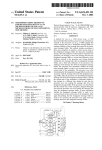
With reference noW to FIG. 3, there can be seen a
high-level block diagram of the XA-C3 microcontroller 20.
The XA-C3 microcontroller 20 includes the folloWing func
The DMA engine 38, the MMRs 40, and the CCB 42 can
collectively be considered to constitute a CAN/ CAL module
77, and Will be referred to as such at various times through
15
folloWing description.
As previously mentioned, the XA-C3 microcontroller 20
automatically implements, in hardWare, many message man
agement and other functions that Were previously only
implemented in softWare running on the host CPU (or not
tional blocks that are fabricated on a single integrated circuit
(IC) chip packaged in a 44-pin PLCC or a 44-pin LQFP
package:
an XA CPU Core 22, that is currently implemented as a
implemented at all), including transparent, automatic
16-bit fully static CPU With 24-bit program and data
address range, that is upWardly compatible With the
80C51 architecture, and that has an operating fre
quency of up to 30 MHZ;
a program or code memory 24 that is currently imple
re-assembly of up to 32 concurrent, interleaved, multi
frame, fragmented CAL messages. For each application that
is installed to run on the host CPU (i.e., the XA CPU Core
25
22), the user (softWare programmer) must set-up the hard
Ware for performing these functions by programming certain
ones of the MMRs and SFRs in the manner set forth in the
mented as a 32K ROM/EPROM, and that is
bi-directionally coupled to the XA CPU Core 22 via an
internal Program bus 25. A map of the code memory
XA-C3 Functional Speci?cation and XA-C3 CAN Transport
Layer Controller User Manual. The register programming
space is depicted in FIG. 4;
a Data RAM 26 (internal or scratch pad data memory) that
is currently implemented as a 1024 Byte portion of the
procedures that are most relevant to an understanding of the
present invention are described beloW, folloWed by a
description of the various message management and other
functions that are automatically performed by the CAL/
CAN module 77 during operation of the XA-C3 microcon
troller 20 after it has been properly set-up by the user.
overall XA-C3 data memory space, and that is
bi-directionally coupled to the XA CPU Core 22 via an
internal DATA bus 27;
an on-chip message buffer RAM or XRAM 28 that is
35
currently implemented as a 512 Byte portion of the
provided.
overall XA-C3 data memory space Which may contain
part or all of the CAN/CAL (Transmit & Receive
Set-up/Programming Procedures
As an initial matter, the user must map the overall XA-C3
Object) message buffers;
data memory space, as illustrated in FIG. 5. In particular,
subject to certain constraints, the user must specify the
starting or base address of the XRAM 28 and the starting or
base address of the MMRs 40. The base address of the
a Memory Interface (MIF) unit 30 that provides interfaces
to generic memory devices such as SRAM, DRAM,
?ash, ROM, and EPROM memory devices via an
external address/data bus 32, via an internal Core Data
bus 34, and via an internal MMR bus 36;
a DMA engine 38 that provides 32 CAL DMA Channels;
45
priately programming the MMRs designated MBXSR and
XRAMB (see FIG. 4).
(MMRs) 40 that are mapped to the overall XA-C3 data
memory space—a 4K Byte portion of the overall
The user can place the 4 KByte space reserved for MMRs
XA-C3 data memory space is reserved for MMRs.
40 anyWhere Within the entire 16 Mbyte data memory space
supported by the XA architecture, other than at the very
bottom of the memory space (i.e., the ?rst 1 KByte portion,
starting address of 000000h), Where it Would con?ict With
These MMRs include 32 (Message) Object or Address
Pointers and 32 ID Screeners or Match IDs, corre
the on-chip Data RAM 26 that serves as the internal or
55
a 2.0B CAN/DLL Core 42 that is the CAN Controller
the “CAN Core Block” (CCB)); and,
disabled. The ?rst 512 Bytes (offset 000h—1FFh) of MMR
space are the Message Object Registers (eight per Message
an array of standard microcontroller peripherals that are
bi-directionally coupled to the XA CPU Core 22 via a
& Timer 1 included in Timer block 53, and Timer 2
scratch-pad memory. The 4 KBytes of MMR space Will
alWays start at a 4K boundary. The reset values for MRBH
and MRBL are OFh and FOh, respectively. Therefore, after a
reset, the MMR space is mapped to the uppermost 4K Bytes
of Data Segment OFh, but access to the MMRs 40 is
Core from the Philips SJA1000 CAN (2.0A/B) Data
Link Layer (CDLL) device (hereinafter referred to as
§pecial Eunction Register (SFR) bus 43. These stan
dard microcontroller peripherals include Universal
Asynchronous Receiver Transmitter (UART) 49, an
SPI serial interface (port) 51, three standard timers/
counters With toggle output capability, namely, Timer 0
MMRs 40 can be speci?ed by appropriately programming
§pecial Eunction Registers (SFRs) MRBL and MRBH. The
base address of the XRAM 28 can be speci?ed by appro
a plurality of on-chip Memory Mapped Registers
sponding to the 32 CAL Message Objects. A complete
listing of all MMRs is provided in the Table depicted in
FIG. 5;
FolloWing these sections, a more detailed description of the
particular invention to Which this application is directed is
Object) for objects n=0—31, as is shoWn in FIG. 6.
The base address of the XRAM 28 is determined by the
65
contents of the MMRs designated MBXSR and XRAMB, as
is shoWn in FIGS. 7 and 8. As previously mentioned, the 512
Byte XRAM 28 is Where some (or all) of the 32 (RX/TX)
message buffers (corresponding to Message Objects
US 6,732,255 B1
7
8
n=0—31) reside. The message buffers can be extended off
The upper 8 bits of the 24-bit address, for all Message
Objects, are speci?ed by the contents of the MBXSR
register, as previously discussed, so that the message buffers
for all Message Objects reside Within the same 64 KByte
memory segment. The user is also responsible, on set-up, for
specifying the siZe of the message buffer for each Message
Object n. In particular, the user can specify the siZe of the
message buffer for each particular Message Object n by
programming the MnBSZ register associated With that Mes
sage Object n. The top location of the message buffer for
each Message Object n is determined by the siZe of that
message buffer as speci?ed in the corresponding MnBSZ
chip to a maximum of 8 KBytes. This off-chip expansion
capability can accommodate up to thirty-tWo, 256-Byte
message buffers. Since the uppermost 8 bits of all message
buffer addresses are formed by the contents of the MBXSR
register, the XRAM 28 and all 32 message buffers must
reside in the same 64K Byte data memory segment. Since
the XA-C3 microcontroller 20 only provides address lines
A0—A19 for accessing external memory, all external
memory addresses must be Within the loWest 1 MByte of
address space. Therefore, if there is external memory in the
system into Which any of the 32 message buffers Will be
mapped, then all 32 message buffers and the XRAM 28 must
also be mapped entirely into that same 64K Byte segment,
Which must be beloW the 12 MByte address limit.
register.
15
After the memory space has been mapped, the user can
set-up or de?ne up to 32 separate Message Objects, each of
The user can con?gure (program) the MnCTL register
associated With each particular Message Object n in order to
enable or disable that Message Object n, in order to de?ne
or designate that Message Object n as a Tx or Rx Message
Object; in order to enable or disable automatic hardWare
Which can be either a Transmit (Tx) or a Receive (Rx)
Message Object. A Rx Message Object can be associated
assembly of fragmented Rx messages (i.e., automatic frag
either With a unique CAN ID, or With a set of CAN IDs
mented message handling) for that Message Object n; in
Which share certain ID bit ?elds. As previously mentioned,
each Message Object has its oWn reserved block of data
memory space (up to 256 Bytes), Which is referred to as that
Message Object’s message buffer. As Will be seen, both the
siZe and the base address of each Message Object’s message
buffer is programmable.
As previously mentioned, each Message Object is asso
order to enable or disable automatic generation of a
Message-Complete Interrupt for that Message Object n; and,
in order to enable or not enable that Message Object n for
Remote Transmit Request (RTR) handling. In CANopen and
25
As previously mentioned, on set-up, the user must con
?gure (program) the global GCTL register, Whose bits
control global parameters that apply to all Message Objects.
ciated With a set of eight MMRs 40 dedicated to that
Message Object. Some of these registers function differently
for Tx Message Objects than they do for Rx Message
Objects. These eight MMRs 40 are designated “Message
In particular, the user can con?gure (program) the GCTL
register in order to specify the high-level CAL protocol (if
any) being used (e.g., DeviceNet, CANopen, or OSEK); in
Object Registers” (see FIG. 4).
The Names of These Eight MMRs 40 Are:
1. MnMIDH Message n Match ID High
. MnMIDL Message n Match ID LoW
OSEK systems, the user must also initialiZe the MnFCR
register associated With each Message Object n.
order to enable or disable automatic acknowledgment of
CANopen Frames (CANopen auto-acknoWledge); and, in
35
. MnMSKH Message n Mask High
. MnMSKL Message n Mask LoW
. MnCTL Message n Control
order to specify Which of tWo transmit (Tx) pre-arbitration
schemes/policies is to be utiliZed (i.e., either Tx pre
arbitration based on CAN ID, With the object number being
used as a secondary tie-breaker, or Tx pre-arbitration based
on object number only).
Receive Message Objects and the Receive Process
During reception (i.e., When an incoming CAN Frame is
being received by the XA-C3 microcontroller 20), the CAN/
. MnBLR Message n Buffer Location Register
. MnBSZ Message n Buffer SiZe
8. MnFCR Message n Fragment Count Register
Where n ranges from 0 to 31 (i.e., corresponding to 32
CAL module 77 Will store the incoming CAN Frame in a
independent Message Objects).
temporary (13-Byte) buffer, and determine Whether a
complete, error-free CAN frame has been successfully
In general, the user de?nes or sets up a Message Object
45
by con?guring (programming) some or all of the eight
received. If it is determined that a complete, error-free CAN
MMRs dedicated to that Message Object, as Will be
described beloW. Additionally, as Will be described beloW,
Frame has been successfully received, then the CAN/CAL
module 77 Will initiate Acceptance Filtering in order to
the user must con?gure (program) the global GCTL register,
Whose bits control global parameters that apply to all
determine Whether to accept and store that CAN Frame, or
to ignore/discard that CAN Frame.
Message Objects.
Acceptance Filtering
In general, because the XA-C3 microcontroller 20 pro
vides the user With the ability to program separate Match ID
In particular, the user can specify the Match ID value for
each Message Object to be compared against the Screener
IDs extracted from incoming CAN Frames for Acceptance
Filtering. The Match ID value for each Message Object n is
speci?ed in the MnMIDH and MnMIDL registers associated
and Mask ?elds for each of the 32 independent Message
55
Objects, on an object-by-object basis, as described
previously, the Acceptance Filtering process performed by
With that Message Object n. The user can mask any Screener
ID bits Which are not intended to be used in Acceptance
“match and mask” technique. The basic objective of this
Filtering, on an object-by-object basis, by Writing a logic ‘1’
in the desired (to-be-masked) bit position(s) in the appro
priate MnMSKH and/or MnMSKL registers associated With
each particular Message Object n. The user is responsible,
Acceptance Filtering process is to determine Whether a
Screener ID ?eld of the received CAN Frame (excluding the
“don’t care” bits masked by the Mask ?eld for each Message
Object) matches the Match ID of any enabled one of the 32
on set-up, for assigning a unique message buffer location for
each Message Object n. In particular, the user can specify the
least signi?cant 16 bits of the base address of the message
Message Objects that has been designated a Receive Mes
the XA-C3 microcontroller 20 can be characteriZed as a
buffer for each particular Message Object n by programming
sage Object. If there is a match betWeen the received CAN
Frame and more than one Message Object, then the received
CAN Frame Will be deemed to have matched the Message
the MnBLR register associated With that Message Object n.
Object With the loWest object number
65
US 6,732,255 B1
9
10
Acceptance Filtering is performed as follows by the
tially to the appropriate message buffer location until the
Whole accepted CAN Frame is transferred. After the DMA
engine 38 has successfully transferred an accepted CAN
Frame to the appropriate message buffer location, the con
tents of the message buffer Will depend upon Whether the
message that the CAN Frame belongs to is a non-fragmented
(single frame) message or a fragmented message. Each case
is described beloW:
XA-C3 microcontroller 20:
(1) A Screener ID ?eld is extracted from the incoming
(received) CAN Frame. In this regard, the Screener ID
?eld that is assembled from the incoming bit stream is
different for Standard and Extended CAN Frames. In
particular, as is illustrated in FIG. 9, the Screener ID ?eld
for a Standard CAN Frame is 28 bits, consisting of 11
CAN ID bits extracted from the header of the received
CAN Frame+2><8 (16) bits from the ?rst and second data
Non-Fragmented Message Assembly:
For Message Objects that have been set up With automatic
fragmented message handling disabled (not enabled—i.e.,
bytes (Data Byte 1 and Data Byte 2) of the received CAN
the FRAG bit in the MnCTL register for that Message
Object is set to ‘0’), the complete CAN ID of the accepted
CAN Frame (Which is either 11 or 29 bits, depending on
Frame+the IDE bit. Thus, the user is required to set the
Msk1 and Msk0 bits in the Mask Field (MnMSKL
register) for Standard CAN Frame Message Objects, i.e.,
to “don’t care”. In addition, in many applications based on
Whether the accepted CAN Frame is a Standard or Extended
15
Standard CAN Frames, either Data Byte 1, Data Byte 2,
CAN Frame) is Written into the MnMIDH and MnMIDL
registers associated With the Message Object that has been
or both do not participate in Acceptance Filtering. In those
deemed to constitute a match, once the DMA engine 38 has
applications, the user must also mask out the unused Data
successfully transferred the accepted CAN Frame to the
message buffer associated With that Message Object. This
Byte(s). The IDE bit is not maskable. As is illustrated in
FIG. 10, the Screener ID ?eld for an Extended CAN
Will permit the user application to see the exact CAN ID
Which resulted in the match, even if a portion of the CAN ID
Was masked for Acceptance Filtering. As a result of this
mechanism, the contents of the MnMIDH and MnMIDL
registers can change every time an incoming CAN Frame is
Frame is 30 bits, consisting of 29 CAN ID bits extracted
from the header of the incoming CAN Frame+the IDE bit.
Again, the IDE bit is not maskable.
(2) The assembled Screener ID ?eld of the received CAN
Frame is then sequentially compared to the corresponding
25
Match ID values speci?ed in the MnMIDH and MnMIDL
registers for all currently enabled Receive Message
the bits that are masked out Will change. Therefore, the
criteria for match and mask Acceptance Filtering Will not
Objects. Of course, any bits in the Screener ID ?eld that
are masked by a particular Message Object are not
included in the comparison. That is, if there is a ‘1’ in a
change as a result of the contents of the MnMIDH and
MnMIDL registers being changed in response to an accepted
incoming CAN Frame being transferred to the appropriate
bit position of the Mask ?eld speci?ed in the MnMSKH
and MnMSKL registers for a particular Message Object,
then the corresponding bit position in the Match ID ?eld
for that particular Message Object becomes a “don’t
care”, i.e., alWays yields a match With the corresponding
accepted. Since the incoming CAN Frame must pass
through the Acceptance Filter before it can be accepted, only
message buffer.
Fragmented Message Assembly:
For Message Objects that have been set up With automatic
35
bit of the Screener ID of the received CAN Frame.
(3) If the above comparison process yields a match With
fragmented message handling enabled (i.e., With the FRAG
bit in the MnCTL register for that Message Object set to ‘1’),
more than one Message Object, then the received CAN
Frame Will be deemed to have matched the Message
masking of the 11/29 bit CAN ID ?eld is disalloWed. As
such, the CAN ID of the accepted CAN Frame is knoWn
unambiguously, and is contained in the MnMIDH and
Object having the loWest object number
MnMIDL registers associated With the Message Object that
Message Storage:
has been deemed to constitute a match. Therefore, there is no
Each incoming (received) CAN Frame that passes Accep
tance Filtering, Will be automatically stored, via the DMA
engine 38, into the message buffer for the Receive Message
need to Write the CAN ID of the accepted CAN Frame into
the MnMIDH and MnMIDL registers associated With the
Message Object that has been deemed to constitute a match.
As subsequent CAN Frames of a fragmented message are
received, the neW data bytes are appended to the end of the
Object that particular CAN Frame Was found to have
matched. In an exemplary implementation, the message
buffers for all Message Objects are contained in the XRAM
28.
45
previously received and stored data bytes. This process
Message Assembly:
continues until a complete multi-frame message has been
received and stored in the appropriate message buffer.
In general, the DMAengine 38 Will transfer each accepted
CAN Frame from the 13-byte pre-buffer to the appropriate
if a Message Object is an enabled Receive Message Object,
Under CAL protocols DeviceNet, CANopen, and OSEK,
and its associated MnCTL register has its FRAG bit set to ‘ 1’
message buffer (e.g., in the XRAM 28), one Word at a time,
starting from the address pointed to by the contents of the
MBXSR and MnBLR registers. Every time the DMA engine
38 transfers a byte or a Word, it has to request the bus. In this
regard, the MIF unit 30 arbitrates betWeen accesses from the
55
XA CPU Core 22 and from the DMA engine 38. In general,
(i.e., automatic fragmented message assembly is enabled for
that particular Receive Message Object), then the ?rst data
byte (Data Byte 1) of each received CAN Frame that
matches that particular Receive Message Object Will be used
to encode fragmentation information only, and thus, Will not
be stored in the message buffer for that particular Receive
bus arbitration is done on an “alternate” policy. After a DMA
bus access, the XA CPU Core 22 Will be granted bus access,
if requested. After an XA CPU bus access, the DMA engine
Message Object. Thus, message storage for such “FRAG
38 Will be granted bus access, if requested. (HoWever, a
data byte (Data Byte 2) and proceed in the previously
enabled” Receive Message Objects Will start With the second
burst access by the XA CPU Core 22 cannot be interrupted
described manner until a complete multiframe message has
by a DMA bus access).
Once bus access is granted by the MIF unit 30, the DMA
engine 38 Will Write data from the 13-byte pre-buffer to the
appropriate message buffer location. The DMA engine 38
been received and stored in the appropriate message buffer.
This message storage format is illustrated in FIG. 11. The
message handler hardWare Will use the fragmentation infor
mation contained in Data Byte 1 of each CAN Frame to
facilitate this process.
Will keep requesting the bus, Writing message data sequen
65
US 6,732,255 B1
11
12
Under the CAN protocol, if a Message Object is an
message is ready to be transmitted (i.e., if more than one
Transmit Message Object is enabled), a TX Pre-Arbitration
enabled Receive Message Object, and its associated MnCTL
register has its FRAG bit set to ‘1’ (i.e., automatic frag
mented message assembly is enabled for that particular
Receive Message Object), then the CAN Frames that match
that particular Receive Message Object Will be stored
sequentially in the message buffer for that particular Receive
Message Object using the format shoWn in FIG. 12.
process Will be performed to determine Which enabled
Transmit Message Object Will be selected for transmission.
There are tWo TX Pre-Arbitration policies Which the user can
choose betWeen by setting or clearing the PreiArb bit in the
GCTL register.
After a TX Message Complete interrupt is generated in
When Writing message data into a message buffer asso
ciated With a Message Object n, the DMA engine 38 Will
10
generate addresses automatically starting from the base
address of that message buffer (as speci?ed in the MnBLR
register associated With that Message Object n). Since the
begins again. Also, if the “Winning” Transmit Message
siZe of that message buffer is speci?ed in the MnBSZ
register associated With that Message Object n, the DMA
response to a determination being made by the message
handler that a completed message has been successfully
transmitted, the TX Pre-Arbitration process is “reset”, and
15
engine 38 can determined When it has reached the top
location of that message buffer. If the DMA engine 38
determines that it has reached the top location of that
message buffer, and that the message being Written into that
message buffer has not been completely transferred yet, the
DMA engine 38 Will Wrap around by generating addresses
starting from the base address of that message buffer again.
Some time before this happens, a Warning interrupt Will be
Object subsequently loses arbitration on the CAN bus, the
TX Pre-Arbitration process gets reset and begins again. If
there is only one Transmit Message Object Whose OBJiEN
bit is set, it Will be selected regardless of the TX Pre
Arbitration policy selected.
Once an enabled Transmit Message Object has been
selected for transmission, the DMA engine 38 Will begin
retrieving the transmit message data from the message buffer
associated With that Transmit Message Object, and Will
begin transferring the retrieved transmit message data to the
CCB 42 for transmission. The same DMA engine and
address pointer logic is used for message retrieval of trans
generated so that the user application can take the necessary
mit messages as is used for message storage of receive
25 messages, as described previously. Further, message buffer
action to prevent data loss.
location and siZe information is speci?ed in the same Way,
The message handler Will keep track of the current
address location of the message buffer being Written to by
as described previously. In short, When a transmit message
the DMA engine 38, and the number of bytes of each CAL
message as it is being assembled in the designated message
is retrieved, it Will be Written by the DMA engine 38 to the
CCB 42 sequentially. During this process, the DMA engine
38 Will keep requesting the bus; When bus access is granted,
the DMA engine 38 Will sequentially read the transmit
buffer. After an “End of Message” for a CAL message is
decoded, the message handler Will ?nish moving the com
plete CAL message and the Byte Count into the designated
message buffer via the DMA engine 38, and then generate an
interrupt to the XA CPU Core 22 indicating that a complete
message has been received.
Since Data Byte 1 of each CAN Frame contains the
fragmentation information, it Will never be stored in the
designated message buffer for that CAN Frame. Thus, up to
seven data bytes of each CAN Frame Will be stored. After
message data from the location in the message buffer cur
rently pointed to by the address pointer logic; and, the DMA
engine 38 Will sequentially Write the retrieved transmit
35
a message for transmission, the user application must not
include the CAN ID and Frame Information ?elds in the
transmit message data Written into the designated message
buffer, since the Transmit (TX) logic Will retrieve this
information directly from the appropriate MnMIDH,
MnMIDL, and MnMSKH registers.
the entire message has been stored, the designated message
buffer Will contain all of the actual informational data bytes
received (exclusive of fragmentation information bytes) plus
the Byte Count at location 00 Which Will contain the total
number of informational data bytes stored.
It is noted that there are several speci?c user set-up/
message data to the CCB 42. It is noted that When preparing
The XA-C3 microcontroller 20 does not handle the trans
45
mission of fragmented messages in hardWare. It is the user’s
responsibility to Write each CAN Frame of a fragmented
message to the appropriate message buffer, enable the asso
programming procedures that must be folloWed When invok
ciated Transmit Message Object for transmission, and Wait
ing automatic hardWare assembly of fragmented OSEK and
for a completion before Writing the neXt CAN Frame of that
fragmented message to the appropriate message buffer. The
user application must therefore transmit multiple CAN
Frames one at a time until the Whole multi-frame, frag
mented transmit message is successfully transmitted.
CANopen messages. These and other particulars can be
found in the XA-C3 CAN Transport Layer Controller User
Manual that is part of the parent Provisional Application
Serial No. 60/154,022, the disclosure of Which has been
fully incorporated herein for all purposes.
Transmit Message Objects and the Transmit Process
In order to transmit a message, the XA application pro
gram must ?rst assemble the complete message and store it
HoWever, by using multiple Transmit Message Objects
Whose object numbers increase sequentially, and Whose
CAN IDs have been con?gured identically, several CAN
55
in the designated message buffer for the appropriate Trans
mit Message Object n. The message header (CAN ID and
Frame Information) must be Written into the MnMIDH,
MnMIDL, and MnMSKH registers associated With that
Transmit Message Object n. After these steps are completed,
the XA application is ready to transmit the message. To
initiate a transmission, the object enable bit (OBJiEN bit)
of the MnCTL register associated With that Transmit Mes
sage Object n must be set, eXcept When transmitting an
Auto-Acknowledge Frame in CANopen. This Will alloW this
ready-to-transmit message to participate in the pre
arbitration process. In this connection, if more than one
Frames of a fragmented transmit message can be queued up
and enabled, and then transmitted in order.
To avoid data corruption When transmitting messages,
there are three possible approaches:
1. If the TX Message Complete interrupt is enabled for the
transmit message, the user application Would Write the
neXt transmit message to the designated transmit message
buffer upon receipt of the TX Message Complete interrupt.
Once the interrupt ?ag is set, it is knoWn for certain that
the pending transmit message has already been transmit
65
ted.
2. Wait until the OBJiEN bit of the MnCTL register of the
associated Transmit Message Object clears before Writing
US 6,732,255 B1
14
13
to the associated transmit message buffer. This can be
The Present Invention
accomplished by polling the OBJiEN bit of the MnCTL
register of the associated Transmit Message Object.
XA-C3 microcontroller 20 can be segmented into various
3. Clear the OBJiEN bit of the MnCTL register of the
associated Transmit Message Object While that Transmit
Message Object is still in TX Pre-Arbitration.
In the ?rst tWo cases above, the pending transmit message
Will be transmitted completely before the neXt transmit
message gets transmitted. For the third case above, the
As previously described, the overall memory space of the
regions or blocks, including the folloWing:
5
mented as a 32K ROM/EPROM and that is
bi-directionally coupled to the XA CPU Core 22 via the
internal Program bus 25);
transmit message Will not be transmitted. Instead, a transmit
an on-chip or off-chip internal or scratch pad data memory
message With neW content Will enter TX Pre-Arbitration.
space (e.g., the Data RAM 26 that is currently imple
There is an additional mechanism that prevents corruption
of a message that is being transmitted. In particular, if a
transmission is ongoing for a Transmit Message Object, the
user Will be prevented from clearing the OBJiEN bit in the
MnCTL register associated With that particular Transmit
mented as a 1024 Byte portion of the overall XA-C3
data memory space, and that is bi-directionally coupled
15
Message Object.
CAN/CAL Related Interrups
on-chip memory mapped registers (e.g., the on-chip
20
1. RX Message Complete
2. TX Message Complete
3. RX Buffer Full
MMRs 40 that constitute a 4K Byte portion of the
overall XA-C3 data memory space).
As Was previously described in detail hereinabove, the
overall XA-C3 memory space constitutes a contiguous
address space, even though some memory regions reside in
4. Message Error
5. Frame Error
to the XA CPU Core 22 via the internal DATA bus 27);
an on-chip or off-chip message buffer memory space (e. g.,
the on-chip message buffer RAM or XRAM 28 that is
currently implemented as a 512 Byte portion of the
overall XA-C3 data memory space); and,
The CAN/CAL module 77 of the XA-C3 microcontroller
20 is presently con?gured to generate the folloWing ?ve
different Event interrupts to the XA CPU Core 22:
an on-chip or off-chip program memory space (e.g., the
program or code memory 24 that is currently imple
25
For single-frame messages, the “Message Complete” con
physically separate on-chip and/or off-chip memory devices,
and other memory regions are just arbitrary partitions of a
dition occurs at the end of the single frame. For multi-frame
common physical memory space, based on address. Further,
(fragmented) messages, the “Message Complete” condition
the on-chip message buffers (the XRAM 28) and the on-chip
MMRs 40, along With all of the off-chip memories, appear
occurs after the last frame is received and stored. Since the
XA-C3 microcontroller 20 hardWare does not recogniZe or
handle fragmentation for transmit messages, the TX Message
Complete condition Will alWays be generated at the end of
each successfully transmitted frame.
As previously mentioned, there is a control bit associated
With each Message Object indicating Whether a Message
Complete condition should generate an interrupt, or just set
30
interface (i.e., the MIF unit 30).
The XA CPU Core 22 must regularly access all of these
memory regions. In addition, the DMA engine 38 Within the
35
a “Message Complete Status Flag” (for polling) Without
generating an interrupt. This is the INTiEN bit in the
MnCTL register associated With each Message Object n.
There are tWo 16-bit MMRs 40, MCPLH and MCPLL,
Which contain the Message Complete Status Flags for all 32
as off-chip RAM to the XA CPU Core 22 and are accessed
as such using the same address lines and eXternal memory
40
CAN/CAL module 77 must regularly access the on-chip and
off-chip message buffer space Where incoming messages are
stored and from Which outgoing messages are retrieved. If
the memory accesses by the DMA engine 38 routinely
interfered With the “eXternal” memory accesses by the XA
CPU Core 22, and/or conversely, if the memory accesses by
the XA CPU Core 22 routinely interfered With the memory
Message Objects. When a Message Complete (TX or RX)
accesses by the DMA engine 38, system performance Would
condition is detected for a particular Message Object, the
corresponding bit in the MCPLH or MCPLL register Will be
be severely degraded.
set. This Will occur regardless of Whether the INTiEN bit
In order to minimiZe such memory access con?icts, in
45
is set for that particular Message Object (in its associated
MNCTL register), or Whether Message Complete Status
Flags have already been set for any other Message Objects.
In addition to these 32 Message Complete Status Flags,
there is a TX Message Complete Interrupt Flag and an RX
50
accordance With the present invention, the XA-C3 micro
controller 20 is con?gured to permit the XA CPU Core 22
and the DMA engine 38 to concurrently access “eXternal”
memory regions provided they are not both addressing the
same memory segment at the same time. Speci?cally, the
XA CPU Core 22 is permitted to access any off-chip
Message Complete Interrupt Flag, corresponding to bits [1]
memory region or the on-chip MMRs 40 While the DMA
and [0], respectively, of an MMR 40 designated
CANINTFLG, Which Will generate the actual Event inter
engine 38 is accessing the on-chip message buffer space
(i.e., the XRAM 28). Alternatively, or additionally, the XA
rupt requests to the XA CPU Core 22. When an End-of
Message condition occurs, at the same moment that the
55
While the DMA engine 38 is accessing the off-chip message
buffer space (if provided). If, hoWever, both the XA CPU
Message Complete Status Flag is set, the appropriate TX or
RX Message Complete Interrupt ?ip-?op Will be set pro
vided that INTiEN=1 for the associated Message Object,
and provided that the interrupt is not already set and pend
1ng.
CPU Core 22 could be permitted to access the on-chip
message buffer space (i.e., the XRAM 28) or the MMRs 40
Core 22 and the DMA engine 38 are simultaneously request
ing access to any off-chip memory region, or if both are
60
Further details regarding the generation of interrupts and
simultaneously requesting access to the on-chip message
buffer space (i.e., the XRAM 28), the MIF unit 30 Will grant
the associated registers can be found in the XA-C3 Func
access to the one of the CPU Core 22 or the DMA engine 38
tional Speci?cation and in the XA-C3 CAN Transport Layer
that Was last denied access, i.e., the “Winner” Will be the
Controller User Manual, both of Which are part of the parent
Provisional Application Serial No. 60/154,022, the disclo
sure of Which has been fully incorporated herein for all
purposes.
65
previous “loser”, as described previously under the section
entitled Message Assembly. For eXample, if both the CPU
Core 22 and the DMA engine 38 are simultaneously request
ing access to the XRAM 28, the MIF unit 30 Will grant
US 6,732,255 B1
15
16
8. A CAN microcontroller that supports a plurality of
access to the CPU Core 22, if the DMA engine 38 Was
previously granted access the last time such a memory
message objects, comprising:
access con?ict occurred.
a processor core that runs CAN applications;
In order to permit concurrent access to different memory
regions, separate address/data buses are provided for any
off-chip memories, for the on-chip message buffer (i.e., the
XRAM 28), and for the on-chip MMRs 40. The MIF unit 30
routes traf?c to/from each bus according to the addresses it
receives. In order to permit the XA CPU Core 22 and the
DMA engine 38 to concurrently access the XRAM 28 and
the off-chip memory, tWo independent arbiters are provided
10
in the MIF unit 30, one dedicated to each memory space.
There is no arbiter provided in the MIF unit 30 for memory
mapped special function register space, because the DMA
engine 38 does not access that memory space and, as such,
the XA CPU Core 22 alWays has immediate access to that
memory space.
15
embodiment/implementation, it should be clearly under
stood that many variations, modi?cations, and/or alternative
25
each of the message objects, the memory-mapped reg
a memory interface unit that permits the processor core
and the CAN/CAL module to concurrently access a
different respective one of the ?rst and second memory
spaces, that permits the processor core and the CAN/
CAL module to concurrently access a different respec
tive one of the ?rst and second memory segments, and
that arbitrates access to the second memory space and
that arbitrates access to the same one of the ?rst and
second memory segments When the processor core and
the CAN/CAL module request concurrent access to the
message objects, comprising:
a processor core that runs CAN applications;
second memory space or to the same one of the ?rst and
a CAN/CAL module that processes incoming messages;
data memory including a ?rst memory segment that
provides a plurality of message buffers associated With
respective ones of the message objects, and a second
memory segment that provides a plurality of memory
mapped registers for each of the message objects, the
memory-mapped registers for each message object
provides a plurality of memory-mapped registers for
isters for each message object containing respective
command/control ?elds for con?guration and setup of
that message object; and,
Although the present invention has been described in
detail hereinabove in the conteXt of a speci?c preferred
embodiments/implementations of the basic inventive con
cepts taught herein Which may appear to those skilled in the
pertinent art Will still fall Within the spirit and scope of the
present invention, as de?ned in the appended claims.
What is claimed is:
1. A CAN microcontroller that supports a plurality of
a CAN/CAL module that processes incoming messages,
Wherein the processor core and the CAN/CAL module
are contained on a single integrated circuit chip;
data memory including a ?rst memory space that is
located on the integrated circuit chip and a second
memory space that is located off the integrated circuit
chip, the ?rst memory space including a ?rst memory
segment that provides at least a portion of a message
buffer memory space that includes a plurality of mes
sage buffers associated With respective ones of the
message objects, and a second memory segment that
second memory segments.
9. The CAN microcontroller as set forth in claim 8,
Wherein the incoming messages include multi-frame, frag
mented messages, and the CAN/CAL module automatically
assembles the multi-frame, fragmented messages.
35
10. The CAN microcontroller as set forth in claim 8,
Wherein the CAN/CAL module includes the memory
containing respective command/control ?elds for con
mapped registers.
?guration and setup of that message object; and,
11. The CAN microcontroller as set forth in claim 8,
Wherein the memory interface unit is contained on the single
a memory interface unit that permits the processor core
and the CAN/CAL module to concurrently access a
different respective one of the ?rst and second memory
integrated circuit chip.
segments, and that arbitrates access to the same one of
the ?rst and second memory segments When the pro
cessor core and the CAN/CAL module request concur
rent access to the same one of the ?rst and second 45
memory segments.
12. The CAN microcontroller as set forth in claim 8,
Wherein the second memory space provides at least a portion
of the message buffer memory space.
13. The CAN microcontroller as set forth in claim 8,
Wherein the memory interface unit includes tWo independent
arbiters dedicated to a respective one of the ?rst and second
memory spaces.
14. The CAN microcontroller as set forth in claim 8,
Wherein the memory interface unit arbitrates access accord
ing to an alternate Winner policy, Wherein a previous loser is
designated a current Winner.
15. A method for operating a CAN microcontroller that
2. The CAN microcontroller as set forth in claim 1,
Wherein the incoming messages include multi-frame, frag
mented messages, and the CAN/CAL module automatically
assembles the multi-frame, fragmented messages.
3. The CAN microcontroller as set forth in claim 1,
Wherein the CAN/CAL module includes the memory
mapped registers.
supports a plurality of message objects, the CAN microcon
4. The CAN microcontroller as set forth in claim 1,
Wherein the processor core, the CAN/CAL module, and the
memory interface unit are contained on a single integrated
troller including a processor core that runs CAN
55
circuit chip.
second memory space that is located off the integrated
circuit chip, the ?rst memory space including a ?rst memory
segment that provides at least a portion of a message buffer
memory space that includes a plurality of message buffers
associated With respective ones of the message objects, and
a second memory segment that provides a plurality of
5. The CAN microcontroller as set forth in claim 4,
Wherein the ?rst and second memory segments are contained
on the integrated circuit chip.
6. The CAN microcontroller as set forth in claim 4,
Wherein the memory interface unit includes tWo independent
arbiters.
7. The CAN microcontroller as set forth in claim 1,
Wherein the memory interface unit arbitrates access accord
applications, a CAN/CAL module that processes incoming
messages, and a data memory including a ?rst memory
space that is located on the integrated circuit chip and a
65
memory-mapped registers for each of the message objects,
the memory-mapped registers for each message object con
ing to an alternate Winner policy, Wherein a previous loser is
taining respective command/control ?elds for con?guration
designated a current Winner.
and setup of that message object, the method comprising:
US 6,732,255 B1
17
18
message objects, the memory-mapped registers for each
permitting the processor core and the CAN/CAL module
to concurrently access a different respective one of the
message object containing respective command/control
?rst and second memory segments; and,
?elds for con?guration and setup of that message object, the
method comprising:
arbitrating access to the same one of the ?rst and second
memory segments When the processor core and the
CAN/CAL module request concurrent access to the
same one of the ?rst and second memory segments.
16. The method as set forth in claim 15, Wherein the
arbitrating access step is performed in accordance With an
alternate Winner policy, Wherein a previous loser is desig
permitting the processor core and the CAN/CAL module
to concurrently access a different respective one of the
?rst and second memory spaces;
permitting the processor core and the CAN/CAL module
10
17. The method as set forth in claim 16, Wherein the
arbitrating access to the second memory space When the
processor core and the CAN/CAL module request
concurrent access to the second memory space; and,
arbitrating step is performed by a memory interface unit
contained in the CAN microcontroller.
18. A method for operating a CAN microcontroller that
supports a plurality of message objects, the CAN microcon
15
arbitrating access to the same one of the ?rst and second
memory segments When the processor core and the
CAN/CAL module request concurrent access to the
troller including a processor core that runs CAN
applications, a CAN/CAL module that processes incoming
?rst and second memory segments.
19. The method as set forth in claim 18, Wherein the
arbitrating access step is performed in accordance With an
messages, and a data memory including a ?rst memory
space that is located on an integrated circuit chip on Which
the CAN microcontroller and the CAN/CAL module are
incorporated, and a second memory space that is located off
alternate Winner policy, Wherein a previous loser is desig
nated a current Winner.
the integrated circuit chip, the ?rst memory space including
a ?rst memory segment that provides at least a portion of a
message buffer memory space that includes a plurality of
message buffers associated With respective ones of the
message objects, and a second memory segment that pro
vides a plurality of memory-mapped registers for each of the
to concurrently access a different respective one of the
?rst and second memory segments;
nated a current Winner.
20. The method as set forth in claim 19, Wherein the
25
arbitrating step is performed by a memory interface unit
contained in the CAN microcontroller.