1
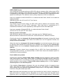
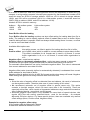
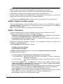
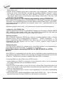
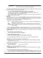
B+K PRECISION’s recommended circuit for AT89Sxxx:
ISP connector
target device
target system
DATA IN
DATA OUT
SCK
RST
target VCC check only
VCC
GND
C1
22n
C2
1u/10V
GND
VCC
R1
R2
R3
MOSI
D2
1N4148
RST
MISO
SCK
I1
AT89Sxxx
R11
100k
GND
GND
GND GND
GND
reset circuit
®
PICmicro microcontrollers
This interface corresponds with Microchip application notes TB013, TB017, TB016: How to
TM
Implement ICSP Using PIC16CXXX OTP (PIC12C5XX OTP)(PIC16F8X Flash) MCUs.
These application notes describes requirement for target system with In-system programming
device and ISP programmer.
®
Following signals are use for In-system programming of PICmicro microcontrollers.
• MCLR\ / VPP reset / switch to programming mode
• RB6 (GP1) clock
• RB7 (GP0) data input / output
• VDD power supply
• GND ground
®
When PICmicro device is programmed, pin MCLR\ / VPP is driven to approximately 12 V.
Therefore, the target system must be isolated from this voltage provided by programmer.
®
RB6 and RB7 signals are used by the PICmicro for In-system programming, therefore target
system mustn’t affect these signals during In-system programming to avoid programming
errors.
Marginal verify is used after programming. Programmer must verify the program memory
®
contents at both minimal and maximal power supply, therefore VDD pin of PICmicro must be
isolated from rest of target system during programming.
136