1
User Manual
FLEX I/O PROFIBUS Adapter Module
Catalog Number 1794-APBDPV1
Important User Information
Solid-state equipment has operational characteristics differing from those of electromechanical equipment. Safety
Guidelines for the Application, Installation and Maintenance of Solid State Controls (publication SGI-1.1 available from
your local Rockwell Automation sales office or online at http://www.rockwellautomation.com/literature/) describes some
important differences between solid-state equipment and hard-wired electromechanical devices. Because of this difference,
and also because of the wide variety of uses for solid-state equipment, all persons responsible for applying this equipment
must satisfy themselves that each intended application of this equipment is acceptable.
In no event will Rockwell Automation, Inc. be responsible or liable for indirect or consequential damages resulting from
the use or application of this equipment.
The examples and diagrams in this manual are included solely for illustrative purposes. Because of the many variables and
requirements associated with any particular installation, Rockwell Automation, Inc. cannot assume responsibility or
liability for actual use based on the examples and diagrams.
No patent liability is assumed by Rockwell Automation, Inc. with respect to use of information, circuits, equipment, or
software described in this manual.
Reproduction of the contents of this manual, in whole or in part, without written permission of Rockwell Automation,
Inc., is prohibited.
Throughout this manual, when necessary, we use notes to make you aware of safety considerations.
WARNING: Identifies information about practices or circumstances that can cause an explosion in a hazardous
environment, which may lead to personal injury or death, property damage, or economic loss.
ATTENTION: Identifies information about practices or circumstances that can lead to personal injury or death,
property damage, or economic loss. Attentions help you identify a hazard, avoid a hazard, and recognize the
consequence
SHOCK HAZARD: Labels may be on or inside the equipment, for example, a drive or motor, to alert people that
dangerous voltage may be present.
BURN HAZARD: Labels may be on or inside the equipment, for example, a drive or motor, to alert people that
surfaces may reach dangerous temperatures.
IMPORTANT
Identifies information that is critical for successful application and understanding of the product.
Allen-Bradley, Rockwell Automation, FLEX I/O, RSLogix, RSLinx, and TechConnect are trademarks of Rockwell Automation, Inc.
Trademarks not belonging to Rockwell Automation are property of their respective companies.
Summary of Changes
The information below summarizes the changes to this manual since the last
printing.
To help you find new and updated information in this release of the manual, we
have included change bars as shown next to this paragraph.
The table below lists the sections that document new features and additional or
updated information about existing features.
Topic
Added detailed procedure for using the teaching feature and the different
parameters for creating a teaching entry
Rockwell Automation Publication 1763-UM002D-EN-P - May 2014
Page
105
iii
Chapter 1
Notes:
iv
Rockwell Automation Publication 1763-UM002D-EN-P - May 2014
Table of Contents
Preface
Who Should Use this Manual . . . . . . . . . . . . . . . . . . . . . . . . . . . . . . . . . . . . . . . v
Purpose of this Manual . . . . . . . . . . . . . . . . . . . . . . . . . . . . . . . . . . . . . . . . . . . . . v
Related Documentation. . . . . . . . . . . . . . . . . . . . . . . . . . . . . . . . . . . . . . . . vi
Common Techniques Used in this Manual . . . . . . . . . . . . . . . . . . . . . . . . . vii
Chapter 1
Overview of the FLEX I/O
PROFIBUS APBDPV1 Module
Overview . . . . . . . . . . . . . . . . . . . . . . . . . . . . . . . . . . . . . . . . . . . . . . . . . . . . . . . . .
The FLEX I/O System. . . . . . . . . . . . . . . . . . . . . . . . . . . . . . . . . . . . . . . . . . . . .
Purpose of the FLEX I/O PROFIBUS APBDPV1 Adapter . . . . . . . . . . .
Differences Between APB and APBDPV1 Adapters . . . . . . . . . . . . . . . . . .
DP-V1 Protocol . . . . . . . . . . . . . . . . . . . . . . . . . . . . . . . . . . . . . . . . . . . . . . .
Functionality. . . . . . . . . . . . . . . . . . . . . . . . . . . . . . . . . . . . . . . . . . . . . . . . . .
Bandwidth and Range. . . . . . . . . . . . . . . . . . . . . . . . . . . . . . . . . . . . . . . . . .
PROFIBUS APBDPV1 Adapter Components. . . . . . . . . . . . . . . . . . . . . . .
Diagnostic Indicators . . . . . . . . . . . . . . . . . . . . . . . . . . . . . . . . . . . . . . . . . .
Network Connector . . . . . . . . . . . . . . . . . . . . . . . . . . . . . . . . . . . . . . . . . . .
Set the Node Address Switches . . . . . . . . . . . . . . . . . . . . . . . . . . . . . . . . .
Power Wiring . . . . . . . . . . . . . . . . . . . . . . . . . . . . . . . . . . . . . . . . . . . . . . . . .
Mount and Remove Your System . . . . . . . . . . . . . . . . . . . . . . . . . . . . . . . . . . .
Optional Accessories . . . . . . . . . . . . . . . . . . . . . . . . . . . . . . . . . . . . . . . . . . . . . .
Extender Cables (1794-CE1 or -CE3) . . . . . . . . . . . . . . . . . . . . . . . . . . .
Mounting Kit (1794-NM1) . . . . . . . . . . . . . . . . . . . . . . . . . . . . . . . . . . . .
Mounting Dimensions and Spacing Requirements . . . . . . . . . . . . . . . . . . .
Chapter Summary . . . . . . . . . . . . . . . . . . . . . . . . . . . . . . . . . . . . . . . . . . . . . . . . .
1
1
2
2
2
2
3
3
3
3
4
4
4
5
5
6
7
7
Chapter 2
Communicate With Your
Module
Overview . . . . . . . . . . . . . . . . . . . . . . . . . . . . . . . . . . . . . . . . . . . . . . . . . . . . . . . . . 9
Communication Over the I/O Backplane . . . . . . . . . . . . . . . . . . . . . . . . . . . 9
Polled I/O Structure. . . . . . . . . . . . . . . . . . . . . . . . . . . . . . . . . . . . . . . . . . . . . . 10
Adapter Input Status Word . . . . . . . . . . . . . . . . . . . . . . . . . . . . . . . . . . . 10
Map Data into the Image Table. . . . . . . . . . . . . . . . . . . . . . . . . . . . . . . . . . . . 12
Logic Status/Analog Feedback Definition . . . . . . . . . . . . . . . . . . . . . . 67
Logic Command/Analog Reference Definition . . . . . . . . . . . . . . . . . 68
Defaults . . . . . . . . . . . . . . . . . . . . . . . . . . . . . . . . . . . . . . . . . . . . . . . . . . . . . . . . . 68
Chapter Summary . . . . . . . . . . . . . . . . . . . . . . . . . . . . . . . . . . . . . . . . . . . . . . . . 69
Chapter 3
Connect Your Adapter to the
PROFIBUS DP Network
v
Overview . . . . . . . . . . . . . . . . . . . . . . . . . . . . . . . . . . . . . . . . . . . . . . . . . . . . . . . .
The DP Physical Layer. . . . . . . . . . . . . . . . . . . . . . . . . . . . . . . . . . . . . . . . . . . .
Cabling and Equipment Required for Line A Type . . . . . . . . . . . . . . . . . .
Cables . . . . . . . . . . . . . . . . . . . . . . . . . . . . . . . . . . . . . . . . . . . . . . . . . . . . . . .
T-junction Connectors . . . . . . . . . . . . . . . . . . . . . . . . . . . . . . . . . . . . . . .
Termination Blocks. . . . . . . . . . . . . . . . . . . . . . . . . . . . . . . . . . . . . . . . . . .
71
71
72
72
72
72
Publication 1794-UM064B-EN-P - May 2014
vi
Table of Contents
Bus Connector . . . . . . . . . . . . . . . . . . . . . . . . . . . . . . . . . . . . . . . . . . . . . . .
Cabling and Equipment Required for Line B Type . . . . . . . . . . . . . . . . . .
Cables . . . . . . . . . . . . . . . . . . . . . . . . . . . . . . . . . . . . . . . . . . . . . . . . . . . . . . .
T-junction Connectors . . . . . . . . . . . . . . . . . . . . . . . . . . . . . . . . . . . . . . .
Termination Blocks. . . . . . . . . . . . . . . . . . . . . . . . . . . . . . . . . . . . . . . . . . .
Bus Connector . . . . . . . . . . . . . . . . . . . . . . . . . . . . . . . . . . . . . . . . . . . . . . .
Connect the Adapter to the Network . . . . . . . . . . . . . . . . . . . . . . . . . . . . . .
Connect Wiring to the Adapter. . . . . . . . . . . . . . . . . . . . . . . . . . . . . . . .
Terminate the Network. . . . . . . . . . . . . . . . . . . . . . . . . . . . . . . . . . . . . . . . . . .
Terminate at the Adapter Using Line A . . . . . . . . . . . . . . . . . . . . . . . .
Terminate at the Adapter Using Line B. . . . . . . . . . . . . . . . . . . . . . . . .
Chapter Summary . . . . . . . . . . . . . . . . . . . . . . . . . . . . . . . . . . . . . . . . . . . . . . . .
73
73
73
73
73
73
74
74
76
76
77
77
Chapter 4
Configure the Adapter for
Master/Slave Communication
Overview . . . . . . . . . . . . . . . . . . . . . . . . . . . . . . . . . . . . . . . . . . . . . . . . . . . . . . . .
How Master/Slave Communication Takes Place . . . . . . . . . . . . . . . . . . . .
Enter User Parameter Data. . . . . . . . . . . . . . . . . . . . . . . . . . . . . . . . . . . . . . . .
User Parameter Data. . . . . . . . . . . . . . . . . . . . . . . . . . . . . . . . . . . . . . . . . .
Auto Configure Format . . . . . . . . . . . . . . . . . . . . . . . . . . . . . . . . . . . . . . .
Condensed Format . . . . . . . . . . . . . . . . . . . . . . . . . . . . . . . . . . . . . . . . . . .
Full Format . . . . . . . . . . . . . . . . . . . . . . . . . . . . . . . . . . . . . . . . . . . . . . . . . .
Enter Check Configuration Data . . . . . . . . . . . . . . . . . . . . . . . . . . . . . . . . . .
Chapter Summary . . . . . . . . . . . . . . . . . . . . . . . . . . . . . . . . . . . . . . . . . . . . . . . .
79
79
80
80
81
81
84
86
89
Chapter 5
Interpret Status Indicators for Overview . . . . . . . . . . . . . . . . . . . . . . . . . . . . . . . . . . . . . . . . . . . . . . . . . . . . . . . . 91
the FLEX I/O PROFIBUS Module Status Indicators . . . . . . . . . . . . . . . . . . . . . . . . . . . . . . . . . . . . . . . . . . . . . . . . . 91
1794-APBDPV1 Module . . . . . . . . . . . . . . . . . . . . . . . . . . . . . . . . . . . . . 91
View status from the Master’s Configuration Software . . . . . . . . . . . . . . 92
Chapter Summary . . . . . . . . . . . . . . . . . . . . . . . . . . . . . . . . . . . . . . . . . . . . . . . . 93
Chapter 6
Apply FLEX I/O Modules
Publication 1794-UM064B-EN-P - May 2014
Overview . . . . . . . . . . . . . . . . . . . . . . . . . . . . . . . . . . . . . . . . . . . . . . . . . . . . . . . .
Evaluate the Application . . . . . . . . . . . . . . . . . . . . . . . . . . . . . . . . . . . . . . . . . .
Define the Area Classification . . . . . . . . . . . . . . . . . . . . . . . . . . . . . . . . . . . . .
Decide Classification Method . . . . . . . . . . . . . . . . . . . . . . . . . . . . . . . . .
Determine Hazard. . . . . . . . . . . . . . . . . . . . . . . . . . . . . . . . . . . . . . . . . . . .
Determine Temperature Rating. . . . . . . . . . . . . . . . . . . . . . . . . . . . . . . .
Select Protection Method(s). . . . . . . . . . . . . . . . . . . . . . . . . . . . . . . . . . . . . . .
Match Field Devices
and I/O Modules. . . . . . . . . . . . . . . . . . . . . . . . . . . . . . . . . . . . . . . . . . . . . . . . .
P/I Analog Transmitter Functional and IS Parameters . . . . . . . . . . .
Loop Functionality Verification . . . . . . . . . . . . . . . . . . . . . . . . . . . . . . .
Chapter Summary . . . . . . . . . . . . . . . . . . . . . . . . . . . . . . . . . . . . . . . . . . . . . . . .
95
95
96
96
96
96
97
97
98
98
99
Table of Contents
vii
Appendix A
Specifications
Overview . . . . . . . . . . . . . . . . . . . . . . . . . . . . . . . . . . . . . . . . . . . . . . . . . . . . . . . 101
Appendix B
Device Data Base (GSD) File
Overview . . . . . . . . . . . . . . . . . . . . . . . . . . . . . . . . . . . . . . . . . . . . . . . . . . . . . . .
Use the Teaching GSD Feature . . . . . . . . . . . . . . . . . . . . . . . . . . . . . . . . . . .
Create Standard and Teaching GSD Files. . . . . . . . . . . . . . . . . . . . . .
Teaching GSD Entry. . . . . . . . . . . . . . . . . . . . . . . . . . . . . . . . . . . . . . . . .
Teach an I/O Module to Work with 1794-APBDPV1 Adapter . . . . .
105
105
106
107
115
Appendix C
Additional HART Protocol
Information
Overview . . . . . . . . . . . . . . . . . . . . . . . . . . . . . . . . . . . . . . . . . . . . . . . . . . . . . . .
Message Structure . . . . . . . . . . . . . . . . . . . . . . . . . . . . . . . . . . . . . . . . . . . . . . .
Master-slave Operation . . . . . . . . . . . . . . . . . . . . . . . . . . . . . . . . . . . . . .
Multiple Master Operation . . . . . . . . . . . . . . . . . . . . . . . . . . . . . . . . . . .
Transaction Procedure . . . . . . . . . . . . . . . . . . . . . . . . . . . . . . . . . . . . . . .
Burst Mode (not supported) . . . . . . . . . . . . . . . . . . . . . . . . . . . . . . . . . .
Universal Commands. . . . . . . . . . . . . . . . . . . . . . . . . . . . . . . . . . . . . . . . . . . .
121
121
121
121
121
122
126
Index
Publication 1794-UM064B-EN-P - May 2014
viii
Table of Contents
Notes:
Publication 1794-UM064B-EN-P - May 2014
Preface
Read this preface to familiarize yourself with the rest of the manual. It provides
information concerning:
•
•
•
•
Who Should Use this
Manual
who should use this manual
the purpose of this manual
related documentation
conventions used in this manual
You must be able to program and operate a PROFIBUS product and PROFIBUS
network to make efficient use of the FLEX I/O PROFIBUS APBDPV1 adapter
module.
We assume you know how to do this in this manual. If you do not, refer to your
software user manuals or online help before attempting to use these modules.
Purpose of this Manual
ix
This manual describes how you can use your FLEX I/O PROFIBUS APBDPV1
adapter with your controller. The manual helps you install, program, and
troubleshoot your module.
For Information About
See
Overview of the FLEX I/O PROFIBUS APBDPV1 Module
Chapter 1
Communicate With Your Module
Chapter 2
Connect Your Adapter to the PROFIBUS DP Network
Chapter 3
Configure the Adapter for Master/Slave Communication
Chapter 4
Interpret Status Indicators for the FLEX I/O PROFIBUS Module
Chapter 5
Apply FLEX I/O Modules
Chapter 6
Specifications
Appendix A
Device Data Base (GSD) File
Appendix B
Additional HART Protocol Information
Appendix C
Publication 1794-UM064B-EN-P - May 2014
x
Related Documentation
The following documents contain additional information concerning Rockwell
Automation products.
Resource
Description
FLEX I/O Selection Guide, publication 1794-SG002.
A description and overview of the 1794 series FLEX I/O, FLEX I/O XT and
FLEX Ex modules and compatible control platforms.
Remote I/O Adapter Module User Manual, publication
1794–UM009.
Information on how to use the Remote I/O Adapter Module
Catalog No. 1794-ASB.
Remote I/O Adapter Modules Installation Instructions,
publication 1794-IN098.
Information on how to install the Remote I/O Adapter Module
Catalog No. 1794-ASB, 1794-ASB2, 1794-ASBK, 1794-ASB2K
FLEX I/O PROFIBUS Adapter Module Installation
Instructions, publication 1794-IN087.
Information on how to install the FLEX I/O PROFIBUS Adapter
Catalog No. 1794-APB.
FLEX I/O PROFIBUS Adapter Module User Manual,
publication 1794-UM057.
Information on how to use the FLEX I/O PROFIBUS Adapter Module
Catalog No. 1794-APB.
FLEX I/O Terminal Base Units Installation Instructions,
publication 1794-IN092.
Information on how to install the FLEX I/O Terminal Base Units
Catalog No. 1794-TB2, 1794-TB3, 1794-TB3K, 1794-TB3S, 1794-TB32,
1794-TB3G, 1794-TB3GK, 1794-TB3GS, 1794-TB3T, 1794-TB3TS, 1794-TBN,
1794-TBNK, 1794-TBNF.
FLEX I/O Digital Input Modules Installation Instructions,
publication 1794-IN093.
Information on how to install the FLEX I/O Digital Input Modules
Catalog No. 1794-IB8, 1794-IB16, 1794-IB16K, 1794-IB32
FLEX I/O Digital DC Sourcing Input and Sinking Output
Modules Installation Instructions, publication
1794-IN095.
Information on how to install the FLEX I/O Digital Input and Output Modules
Catalog No. 1794-IV16, 1794-OV16, 1794-OV16P
FLEX I/O Digital DC Sourcing Output Modules
Installation Instructions, publication 1794-IN094.
Information on how to install the FLEX I/O Digital DC Sourcing Output Modules
Catalog No.1794-OB8, 1794-OB8EP, 1794-OB16, 1794-OB16P, 1794-OB32P
FLEX I/O Input/ Output Module Installation Instructions,
publication 1794-IN083.
Information on how to install the FLEX I/O Input and Output Modules
Catalog No.1794-IB16XOB16P, 1794-IB10XOB6
FLEX I/O 8 Output Relay Module Installation Instructions, Information on how to install the FLEX I/O 8 Output Relay Modules
publication 1794-IN019.
Catalog No.1794-OW8, 1794-OW8K, 1794-OW8XT
FLEX I/O Analog Input and Output Module Installation
Instructions, publication 1794-IN100.
Information on how to install the FLEX I/O Analog Input and Output Modules
Catalog No.1794-IE8, 1794-IE4XOE2, 1794-OE4, 1794-IE8K, 1794-OE4K
FLEX I/O Isolated Analog Output Module Installation
Instructions, publication 1794-IN037.
Information on how to install the FLEX I/O Isolated Analog 4 Input Module
Catalog No.1794-OF4I
FLEX XT I/O Isolated Input Analog Module Installation
Instructions, publication 1794-IN129.
Information on how to install the FLEX I/O Isolated Analog Modules
Catalog No.1794-IF4IXT, 1794-OF4IXT, 1794-IF2XOF2IXT
FLEX I/O Isolated Analog Modules User Manual,
publication 1794-6.5.8.
Information on how to use the FLEX I/O Isolated Analog Modules
Catalog No.1794-IF4I, -OF4I, IF2XOF2I, -IF4IXT, -IF4ICFXT, -OF4IXT, IF2XOF2IXT
FLEX I/O 8 Thermocouple Input Module Installation
Instructions, publication 1794-IN021.
Information on how to install the FLEX I/O Isolated Analog Modules
Catalog No. 1794-IT8,1794-IR8
FLEX I/O Thermocouple/Millivolt Input Module
Installation Instructions, publication 1794-IN050.
Information on how to install the Thermocouple/Millivolt Input Modules
Catalog No. 1794-IRT8, 1794-IRT8K, 1794-IRT8XT
FLEX I/O Thermocouple/Millivolt Input Module User
Manual, publication 1794-6.5.7.
Information on how to use the Thermocouple and Millivolt Input Module
Catalog No. 1794-IT8.
Publication 1794-UM064B-EN-P - May 2014
xi
Resource
Description
FLEX I/O AC Input Modules Installation Instructions,
publication 1794-IN102.
Information on how to install the FLEX I/O AC Input Modules
Catalog No. 1794-IA8, 1794-IA8I, 1794-IA16.
FLEX I/O Digital AC Output Modules Installation
Instructions, publication 1794-IN103.
Information on how to install the FLEX I/O Digital AC Output Modules
Catalog No. 1794-OA8, 1794-OA8K, 1794-OA8I, 1794-OA16.
FLEX I/O DC Power Supply Installation Instructions,
publication 1794-IN069.
Information on how to install the FLEX I/O DC Power Supply
Catalog No. 1794-PS13, 1794-PS3
Interconnect Cable Installation Instructions, publication
1794-5.12.
Information on how to install the extension cables.
Catalog No. 1794--CE1, 1794-CE3
Industrial Automation Wiring and Grounding Guidelines,
publication 1770-4.1.
In-depth information on grounding and wiring Allen-Bradley programmable
controllers.
Allen-Bradley Industrial Automation Glossary,
publication AG-7.1.
A glossary of industrial automation terms and abbreviations.
Common Techniques Used
in this Manual
The following conventions are used throughout this manual:
• Bulleted lists such as this one provide information, not procedural steps.
• Numbered lists provide sequential steps or hierarchical information.
• Italic type is used for emphasis.
Publication 1794-UM064B-EN-P - May 2014
xii
Notes:
Publication 1794-UM064B-EN-P - May 2014
Chapter
1
Overview of the FLEX I/O PROFIBUS
APBDPV1 Module
Overview
Read this chapter to familiarize yourself with the adapter module.
The FLEX I/O System
For Information About
See Page
The FLEX I/O System
1
Purpose of the FLEX I/O PROFIBUS APBDPV1 Adapter
2
Differences Between APB and APBDPV1 Adapters
2
PROFIBUS APBDPV1 Adapter Components
3
Mount and Remove Your System
4
Optional Accessories
5
Mounting Dimensions and Spacing Requirements
7
The FLEX I/O system is a small, modular I/O system for distributed
applications that performs all of the functions of rack-based I/O. The FLEX I/O
system contains the following components:
Adapter
Terminal base
1111
I/O module
1112
1113
• PROFIBUS adapter/power supply – powers the internal logic for as many
as eight I/O modules
• terminal base – contains a terminal strip to terminate wiring for two- or
three-wire devices
• I/O module – contains the bus interface and circuitry needed to perform
specific functions related to your application
1
Publication 1794-UM064B-EN-P - May 2014
2
Overview of the FLEX I/O PROFIBUS APBDPV1 Module
Purpose of the FLEX I/O
PROFIBUS
APBDPV1 Adapter
The 1794-APBDPV1 module is a FLEX I/O communications adapter that
interacts with the FLEX I/O backplane and any PROFIBUS DP master/scanner
controller on a PROFIBUS DP network.
The 1794-APBDPV1 module is a slave device to the DP master/scanner, and is a
master controller of the FLEX I/O system where it is installed. The I/O data
exchange occurs as follows: Output data is sent from the DP master/scanner
controller across the PROFIBUS DP network to the 1794-APBDPV1 adapter.
The adapter then automatically transfers the data across the FLEX I/O backplane
to the output modules. Inputs from the input modules are collected by the FLEX
I/O adapter via the backplane and sent across the PROFIBUS DP network to the
DP master/scanner controller.
PROFIBUS DP
master/scanner
controller
Personal computer
with configuration
software
RS-485
Other DP
adapter/slave
DP
1794-APBDPV1 adapter/slave
Other DP
adapter/slave
FLEX I/O system
Differences Between APB
and APBDPV1 Adapters
1118
This section describes the differences between the 1794-APB FLEX I/O
PROFIBUS and the 1794-APBDPV1 FLEX I/O PROFIBUS APBDPV1
adapter modules.
DP-V1 Protocol
The FLEX I/O PROFIBUS APBDPV1 adapter uses a newer version of
PROFIBUS DP (DP1) protocol whereas the The FLEX I/O PROFIBUS
APB adapter uses the first generation PROFIBUS DP protocol (DP-0).
Functionality
The FLEX I/O PROFIBUS APBDPV1 adapter features Identification &
Maintenance (I&M) functions. These functions specify how certain device
describing data must be unambiguously stored in PROFIBUS devices essentially
enabling easy access to current information on the device. The adapter also
supports newer HART modules than the The FLEX I/O PROFIBUS APB
adapter.
Publication 1794-UM064B-EN-P - May 2014
Overview of the FLEX I/O PROFIBUS APBDPV1 Module
3
Bandwidth and Range
The FLEX I/O PROFIBUS APB adapter baud-rate is now 12 MBd and,
although the physically PROFIBUS address range is still limited to 1..99, the
logical address range is 1..126.
PROFIBUS APBDPV1
Adapter Components
The adapter module consists of the following components:
• two diagnostic indicators
• PROFIBUS DP network connector
• 24V DC power wiring connection terminals
• two node address switches
FlexBus
connector
Status indicator
(green/red)
Node address
switches
PROFIBUS indicator
(green/red)
PROFIBUS DP
network
connector
24V DC wiring
connection
terminals
1119
1120
Diagnostic Indicators
Diagnostic indicators are located on the front panel of the adapter module. They
show both normal operation and error conditions in your FLEX I/O system. The
indicators are:
• Device status (STATUS)
• Communication link status (PROFIBUS)
Upon power-up, the adapter goes to an initialization state and performs a self-test
(memory check, data memory clear, CRC on code). The indicators also go
through a self-test sequence. If a failure occurs, the adapter transitions to a faulted
state and waits for reset (cycle power). Otherwise, the adapter begins monitoring
the network (run state) for messages.
Network Connector
Use the 9-pin SUB-D connector to connect your adapter to the PROFIBUS
network.
Publication 1794-UM064B-EN-P - May 2014
4
Overview of the FLEX I/O PROFIBUS APBDPV1 Module
Set the Node Address Switches
Set the thumbwheel switches to 00 to allow node addressing by software
configuration tool to set the range from 1…125. Address changes take effect only
after cycling power. Use a pen to press either the + or – buttons to change the
number.
Thumbwheel
switches for setting
the node address
9 9
PROFIBUS
DP Network Connector
(9-pin SUB-D)
24V DC wiring
connection
terminals
44560
Power Wiring
Connection terminals are provided for connecting the required 24V DC power
to the front of the module. The power wiring can be daisy-chained to the
terminal base unit located next to the adapter to supply power to the module
installed in that base unit.
Refer to the FLEX I/O PROFIBUS Communications Adapter Installation
Instructions, publication 1794-IN114, that you received with your adapter to
learn how to install and wire the adapter.
Mount and Remove
Your System
You can horizontally or vertically mount the FLEX I/O system on a standard
DIN rail. The adapter and terminal base easily snap on the DIN rail by hand.
Refer to the installation instructions shipped with these components.
Screw holes are also provided to horizontally or vertically panel-mount your
system in an enclosure. To panel-mount your FLEX I/O system, use the optional
mounting kit (1794-NM1). See Example of a DIN Rail-Mounted System on
page 5.
Publication 1794-UM064B-EN-P - May 2014
Overview of the FLEX I/O PROFIBUS APBDPV1 Module
5
Example of a DIN Rail-Mounted System
DIN rail
Allen Bradley catalog number
199-DR1
DIN 46277-3
EN 50022 (35 X 7.5mm)
Screw holes are available for panel-mounting
Components are
slotted to accept
a DIN rail
1114
Locking tab connector holds
terminal base onto DIN rail
Optional Accessories
Extender Cables (1794-CE1 or -CE3)
Use the optional 1794-CE1, 0.3m (11.81 in.) or -CE3, 0.9m (35.43 in.) extender
cable (one per system) to arrange your system in two rows or split your system
into horizontal and vertical orientation.
1794-CE1 or 1794-CE3
extender cable
1115
ATTENTION: Do not use more than one extender cable per system
Publication 1794-UM064B-EN-P - May 2014
6
Overview of the FLEX I/O PROFIBUS APBDPV1 Module
Mounting Kit (1794-NM1)
Use the optional 1794-NM1 mounting kit to mount your system on a panel or
wall without a DIN rail.
1794-NM1
Mounting Kit with
18 screws (2 screws for
the adapter and 2 screws
for each module
1116
Publication 1794-UM064B-EN-P - May 2014
Overview of the FLEX I/O PROFIBUS APBDPV1 Module
7
Mounting Dimensions and
Spacing Requirements
DPV1
21 (0.83)
Optional
mounting
kit
35
(1.4)
94
(3.7)
59
(2.3)
35
(1.4)
23
(0.9)
17
(0.6)
8
(0.3)
80
(3.2)
50
(2.0)
94
(3.7)
80
(3.2)
87
(3.4)
30
(1.2)
68
(2.7)
DIN
Rail
94
(3.7)
For 1794-CE1
Approximately 292.1 (11.5)
from upper connector.
For 1794-CE3
Approximately 901 (35.5)
from upper connector.
1117
Chapter Summary
In this chapter you learned about the FLEX I/O PROFIBUS APBDPV1 adapter
module and the FLEX I/O system. Read the next chapter to learn how to
communicate with your module.
Publication 1794-UM064B-EN-P - May 2014
8
Overview of the FLEX I/O PROFIBUS APBDPV1 Module
Notes:
Publication 1794-UM064B-EN-P - May 2014
Chapter
2
Communicate With Your Module
Overview
Read this chapter to familiarize yourself with configurable features on the input
and output analog modules
Communication Over the
I/O Backplane
For Information About
See Page
Communication Over the I/O Backplane
9
Polled I/O Structure
10
Map Data into the Image Table
12
Defaults
68
One 1794-APBDPV1 PROFIBUS adapter can interface with up to eight
terminal base units with installed FLEX I/O modules, forming a FLEX I/O
system of up to eight slots. The adapter communicates to other network system
components over the PROFIBUS network. The adapter communicates with its
I/O modules over the backplane.
0
Inputs
Read
PROFIBUS
Adapter
Write
Read
Words
Status
Outputs
Write
Words
Configuration
Inputs
Inputs
Status
Status
Outputs
Outputs
Configuration
Configuration
15
1122
The I/O map for a module is divided into read words and write words. Read
words consist of input and status words, and write words consist of output and
configuration words. The number of read words or write words can be 0 or more.
The length of each I/O module’s read words and write words vary in size
depending on module complexity. Each I/O module will support at least 1 input
word or 1 output word. Status and configuration are optional, depending on
the module.
10
Communicate With Your Module
For example, a 16 point discrete input module will have up to 2 read words and 1
write word.
16-point Discrete Input Module
Delay
Time
Delay
Time
1123
Refer to each module user manual I/O map for the exact mapping.
Polled I/O Structure
The first word of output data received by the adapter is the Adapter Status Word.
Output data is received by the adapter in the order of the installed I/O modules.
The Output data for Slot 1 is received first, followed by the Output data for
Slot 2, and so on up to slot 8. All bits in the output status word are reserved.
The first word of input data sent by the adapter is the Adapter Status Word. This
is followed by the input data from each slot, in the order of the installed I/O
modules. The Input data from Slot 1 is first after the status word, followed by
Input data from Slot 2, and so on up to slot 8.
Adapter Status
Slot 1 Input Data
Slot 2 Input Data
Slot 8 Input Data
Read
Write
Adapter Status
Slot 1 Output Data
Slot 2 Output Data
Slot 8 Output Data
Adapter Input Status Word
The input status word consists of:
• I/O module fault bits — 1 status bit for each slot
Publication 1794-UM064B-EN-P - May 2014
1124
Communicate With Your Module
11
• node address changed — 1 bit
Slot 2
Slot 1
Slot 3
Slot 4
8
Slot 5
9
Slot 6
15 14 13 12 11 10
Slot 7
Bit:
Slot 8
I/O Module Fault Bits
7
6
5
4
3
2
1
0
Reserved
Node Address Changed Bit
1125
The adapter input status word bit descriptions are shown in Table Input Status
Word Bits.
Input Status Word Bits
Bit Description
Bit
Explanation
I/O Module Fault
8
This bit is set (1) when an error is detected in slot position 1.
9
This bit is set (1) when an error is detected in slot position 2.
10
This bit is set (1) when an error is detected in slot position 3.
11
This bit is set (1) when an error is detected in slot position 4.
12
This bit is set (1) when an error is detected in slot position 5.
13
This bit is set (1) when an error is detected in slot position 6.
14
This bit is set (1) when an error is detected in slot position 7.
15
This bit is set (1) when an error is detected in slot position 8.
Reserved
1…7
Reserved
Node Address
changed
0
This bit is set (1) when the node address switch setting has been
changed since power up.
Possible causes for an I/O module fault are:
• transmission errors on the FLEX I/O backplane
• a failed module
• a module removed from its terminal base
• an incorrect module inserted in a slot position
• an empty slot
The node address changed bit is set when the node address switch setting has
been changed since power up. The new node address does not take effect until
the adapter has been powered down and then powered back up. Until this power
cycling occurs, the node address switches will not match the actual node address.
Publication 1794-UM064B-EN-P - May 2014
12
Communicate With Your Module
Map Data into the Image
Table
Commonly used FLEX I/O modules used with the PROFIBUS adapter are
listed below. A full list of modules is available in the GSD file. For more
information on the GSD file, see Device Data Base (GSD) File in Appendix B.
FLEX I/O Data Mapping Tables
Module Description
Catalog Number
For image table
mapping see page
8 Sink input module
1794-IB8
12
16 Sink input module
1794-IB16
13
8 Source output module
1794-OB8
14
16 Source output module
1794-OB16
14
16 Source input module
1794-IV16
15
16 Sink output module
1794-OV16
16
8 Electronically fused output module
1794-OB8EP
16
10 input/6 output module
1794-IB10XOB6
17
8 input module
1794-IA8
18
8 output module
1794-OA8
19
8 relay output module
1794-OW8
19
8 input analog module
1794-IE8
20
4 output analog module
1794-OE4
23
4 in/2 out analog combo module
1794-IE4XOE2
25
8 input RTD analog module
1794-IR8
28
8 input thermocouple module
1794-IT8
32
8 input thermocouple/RTD/mV module
1794-IRT8
36
2 input pulse counter module
1794-ID2
59
4 input encoder counter module
1794-IP4
63
SCANport module
1203-FM1
66
1794-IB8 — 8 Point Digital Input Module Image Table Mapping
Filter
Time
1126
Publication 1794-UM064B-EN-P - May 2014
Communicate With Your Module
13
1794-IB8 Memory Map
Decimal Bit
15
14
13
12
11
10
09
08
07
06
05
04
03
02
01
00
Size
Octal Bit
17
16
15
14
13
12
11
10
07
06
05
04
03
02
01
00
Read Words
D7
D6
D5
D4
D3
D2
D1
D0
Read Word 0
Not used
Not used
Read Word 1
Not used
Where:
FT 00…07
Write Word 0
D = Input Data (D0 corresponds to input 0, D1 corresponds to input 1, and so on)
DT = Input Filter Time (FT 00…07 corresponds to inputs 0…7)
1794-IB8 Input Filter Times
Description
Selected
Filter Time
02
01
00
Filter Time for Inputs 00…07
0
0
0
Filter Time 0 (default)
0.256 ms
0
0
1
Filter Time 1
0.512 ms
0
1
0
Filter Time 2
1 ms
0
1
1
Filter Time 3
2 ms
1
0
0
Filter Time 4
4 ms
1
0
1
Filter Time 5
8 ms
1
1
0
Filter Time 6
16 ms
1
1
1
Filter Time 7
32 ms
1794-IB16 – 16-point Digital Input Module Image Table Mapping
Counter
Filter
Time
DF RC
Filter
Time
1127
1794-IB16 Memory Map
Decimal Bit
15
14
13
12
11
10
09
08
07
06
05
04
03
02
01
00
Size
Octal Bit
17
16
15
14
13
12
11
10
07
06
05
04
03
02
01
00
Read Words
D15
D14
D13
D12
D11
D10
D9
D8
D7
D6
D5
D4
D3
D2
D1
D0
Read Word 0
Counter
Not used
Where:
Read Word 1
DF
RC
FT 12…15
FT 00…07
Write Word 0
D = Input Data (D0 corresponds to input 0, D1 corresponds to input 1, and so on)
DT = Input Filter Time (FT 00…11 corresponds to inputs 0…11; FT 12…15 corresponds to inputs 12…15)
DF = Disable Filter
RC = Reset Counter
Publication 1794-UM064B-EN-P - May 2014
14
Communicate With Your Module
1794-IB16 Input Delay Times
Description
Selected
Filter Time
02
01
00
Filter Time for Inputs 00…11
05
04
03
Filter Time for Inputs 12…15
0
0
0
Filter Time 0 (default)
0.256 ms
0
0
1
Filter Time 1
0.512 ms
0
1
0
Filter Time 2
1 ms
0
1
1
Filter Time 3
2 ms
1
0
0
Filter Time 4
4 ms
1
0
1
Filter Time 5
8 ms
1
1
0
Filter Time 6
16 ms
1
1
1
Filter Time 7
32 ms
1794-OB8 – 8 Point Discrete Output Module Image Table Mapping
1128
1794-OB8 Memory Map
Decimal Bit
15
14
13
12
11
10
09
08
07
06
05
04
03
02
01
00
Size
Octal Bit
17
16
15
14
13
12
11
10
07
06
05
04
03
02
01
00
Read Words
Not used
Not used
Read Word 0
O7
O6
O5
O4
O3
Not used
Where:
O2
O1
O0
Write Word 0
Write Word 1
O = Output value (O0 corresponds to output 0, O1 corresponds to output 1, and so on)
1794-OB16 – 16-point Discrete Output Module Image Table Mapping
1130
Publication 1794-UM064B-EN-P - May 2014
Communicate With Your Module
15
1794-OB16 Memory Map
Decimal Bit
15
14
13
12
11
10
09
08
07
06
05
04
03
02
01
00
Size
Octal Bit
17
16
15
14
13
12
11
10
07
06
05
04
03
02
01
00
Read/Write Words
Not used
O15
O14
Read Word 0
O13
O12
O11
O10
O9
O8
O7
O6
O5
O4
O3
O2
O1
O0
Not used
Where:
Write Word 0
Write Word 1
O = Output value (O0 corresponds to output 0, O1 corresponds to output 1, and so on)
1794-IV16 – 16-point Source Input Module Image Table Mapping
Counter
FT for all
Channels
DF RC
1132
1794-IV16 Memory Map
Decimal Bit
15
14
13
12
11
10
09
08
07
06
05
04
03
02
01
00
Size
Octal Bit
17
16
15
14
13
12
11
10
07
06
05
04
03
02
01
00
Read/Write Words
D15
D14
D13
D12
D11
D10
D9
D8
D7
D6
D5
D4
D3
D2
D1
D0
Read Word 0
Counter
Not used
Where:
Read Word 1
DF
RC
NU
FT for all channels
Not used
Write Word 0
D = Input Data (D0 corresponds to input 0, D1 corresponds to input 1, and so on)
DT = Input Filter Time (FT 00…11 corresponds to inputs 0…11; FT 12…15 corresponds to inputs 12…15)
DF = Disable Filter
RC = Reset Counter
NU = Not Used
1794-IV16 Input Filter Times
Description
Selected
Filter Time
10
09
08
Filter Time for Inputs 00-15 (00…17)
0
0
0
Filter Time 0 (default)
216 µs
0
0
1
Filter Time 1
512 µs
0
1
0
Filter Time 2
1 ms
0
1
1
Filter Time 3
2 ms
1
0
0
Filter Time 4
4 ms
Publication 1794-UM064B-EN-P - May 2014
16
Communicate With Your Module
1794-IV16 Input Filter Times
Description
Selected
Filter Time
10
09
08
Filter Time for Inputs 00-15 (00…17)
1
0
1
Filter Time 5
8 ms
1
1
0
Filter Time 6
16 ms
1
1
1
Filter Time 7
32 ms
1794-OV16 – 16-point Sink Output Module Image Table Mapping
1134
1794-OV16 Memory Map
Decimal Bit
15
14
13
12
11
10
09
08
07
06
05
04
03
02
01
00
Size
Octal Bit
17
16
15
14
13
12
11
10
07
06
05
04
03
02
01
00
Read/Write Words
Not used
O15
O14
Read Word 0
O13
O12
Not used
Where:
O11
O10
O9
O8
O7
O6
O5
O4
O3
O2
O1
O0
Write Word 0
Write Word 1
O = Output value
1794-OB8EP – 8-point Discrete Protected Output Module Image Table Mapping
1136
Publication 1794-UM064B-EN-P - May 2014
Communicate With Your Module
17
1794-OB8EP Memory Map
Decimal Bit
15
14
13
12
11
10
09
08
07
06
05
04
03
02
01
00
Size
Octal Bit
17
16
15
14
13
12
11
10
07
06
05
04
03
02
01
00
Read/Write Words
F7
F6
F5
F4
F3
F2
F1
F0
Reserved(1)
FR
O7
Not used
O6
Read Word 0
O5
O4
O3
O2
O1
O0
Reserved
Where:
Write Word 0
Write Word 1
F = overload fault bits – 1 = fault present; 0 = no fault
Ox = Output Data (O0 corresponds to output 0, O1 corresponds to output 1, and so on)
FR = fault reset bit – 1 = reset output; 0 = no change.
Using the Fault Reset Button When you press the manual reset button:
1. The fault indicator for the faulted output turns off for about 1.2 s (the faulted output will not attempt to turn on during this delay)
2. After the 1.2 s delay, the faulted output attempts to turn on
3. If the external condition causing the fault is corrected, the output remains on, the fault indicator is off, and the status indicator is on
(1)
The unused lower byte in read word 1 floats during operation. Do not use this byte for fault status.
1794-IB10XOB6 – 16-point Digital Input/Output Module Image Table Mapping
Filter
Time
1137
1794-IB10XOB6 Memory Map
Decimal Bit
15
14
13
12
11
10
09
08
07
06
05
04
03
02
01
00
Size
Octal Bit
17
16
15
14
13
12
11
10
07
06
05
04
03
02
01
00
Read/Write Words
I9
I8
I7
I6
I5
I4
I3
I2
I1
I0
Read Word 0
Not used
Not used
Read Word 1
Not used
O5
Not used
Where:
Filter Time
O4
O3
Not used
O2
O1
O0
Write Word 0
Write Word 1
I = Input Channel
O = Output Channel
1794-IB10XOB6 Input Filter Times
Description
Selected
Filter Time
02
01
00
Filter Time for Inputs 00…07
0
0
0
Filter Time 0 (default)
0.256 ms
0
0
1
Filter Time 1
0.512 ms
0
1
0
Filter Time 2
1 ms
Publication 1794-UM064B-EN-P - May 2014
18
Communicate With Your Module
1794-IB10XOB6 Input Filter Times
Description
Selected
Filter Time
02
01
00
Filter Time for Inputs 00…07
0
1
1
Filter Time 3
2 ms
1
0
0
Filter Time 4
4 ms
1
0
1
Filter Time 5
8 ms
1
1
0
Filter Time 6
16 ms
1
1
1
Filter Time 7
32 ms
1794-IA8 – 8-point Discrete Input Module Image Table Mapping
Filter
Time
1138
1794-IA8 Memory Map
Decimal Bit
15
14
13
12
11
10
09
08
07
06
05
04
03
02
01
00
Size
Octal Bit
17
16
15
14
13
12
11
10
07
06
05
04
03
02
01
00
Read/Write Words
D7
D6
D5
D4
D3
D2
D1
D0
Read Word 0
Not used
Read Word 1
Not used
Not used
Where:
Not used
FT 00…07
Write Word 0
D = Input Data (D0 corresponds to input 0, D1 corresponds to input 1,and so on)
FT = Input Filter Time (FT 00…07 corresponds to inputs 0…7)
1794-IA8 Input Filter Times
Bits
Publication 1794-UM064B-EN-P - May 2014
Description
Maximum Filter Time
02
01
00
Filter Time for Inputs 00…15 (00…17)
Off to On
On to Off
0
0
0
Filter Time 0 (default)
8.6 ms
26.6 ms
0
0
1
Filter Time 1
9 ms
27 ms
0
1
0
Filter Time 2
10 ms
28 ms
0
1
1
Filter Time 3
12 ms
30 ms
1
0
0
Filter Time 4
17 ms
35 ms
1
0
1
Filter Time 5
26 ms
44 ms
1
1
0
Filter Time 6
43 ms
61 ms
1
1
1
Filter Time 7
78 ms
96 ms
Communicate With Your Module
19
1794-OA8 – 8-point Discrete Output Module Image Table Mapping
1139
1794-OA8 Memory Map
Decimal Bit
15
14
13
12
11
10
09
08
07
06
05
04
03
02
01
00
Size
Octal Bit
17
16
15
14
13
12
11
10
07
06
05
04
03
02
01
00
Read Words
Not used
Read Word 0
O7
Not used
O6
O5
O4
O3
O2
O1
O0
Not used
Where:
Write Word 0
Write Word 1
O = Output value (O0 corresponds to output 0, O1 corresponds to output 1, and so on)
1794-OW8 – 8-point Discrete Relay Output Module Image Table Mapping
1140
1794-OW8 Memory Map
Decimal Bit
15
14
13
12
11
10
09
08
07
06
05
04
03
02
01
00
Size
Octal Bit
17
16
15
14
13
12
11
10
07
06
05
04
03
02
01
00
Read/Write Words
Not used
Not used
Read Word 0
O7
O6
O5
O4
O3
Not used
Where:
O2
O1
O0
Write Word 0
Write Word 1
O = Output value (O0 corresponds to output 0, O1 corresponds to output 1, and so on)
Publication 1794-UM064B-EN-P - May 2014
20
Communicate With Your Module
1794-IE8 Series B – 8 Input Analog Module Image Table Mapping
1141
1794-IE8/B Memory Map
Decimal Bit
15
14
13
12
11
10
09
08
07
06
05
04
03
02
01
00
Size
Octal Bit
17
16
15
14
13
12
11
10
07
06
05
04
03
02
01
00
Read/Write Words
S
Analog Value Channel 0
Read Word 0
S
Analog Value Channel 1
Read Word 1
S
Analog Value Channel 2
Read Word 2
S
Analog Value Channel 3
Read Word 3
S
Analog Value Channel 4
Read Word 4
S
Analog Value Channel 5
Read Word 5
S
Analog Value Channel 6
Read Word 6
S
Analog Value Channel 7
Read Word 7
PU
Not used – set to zero
C7
C6
C5
C4
C3
C2
C1
C0
Not used
Where:
PU = Power up bit – included in series B modules only.
U = Underrange bits for 4…20 mA inputs
C = Configure select bit
F = Full range bit
S = sign bit (in 2’s complement)
Publication 1794-UM064B-EN-P - May 2014
U7
U6
U5
U4
U3
U2
U1
U0
Read Word 8
F7
F6
F5
F4
F3
F2
F1
F0
Write Word 0
Write Word 1…5
Communicate With Your Module
21
1794-IE8/B Range Selection Bits
Channel No.
Channel 0
Channel 1
Channel 2
Channel 3
Channel 4
Channel 5
Channel 6
Channel 7
F0
C0
F1
C1
F2
C2
F3
C3
F4
C4
F5
C5
F6
C6
F7
C7
00
08
(10)
01
09
(11)
02
10
(12)
03
11
(13)
04
12
(14)
04
13
(15)
06
14
(16)
07
15
(17)
0…10V DC/0…20 mA 1
0
1
0
1
0
1
0
1
0
1
0
1
0
1
0
4…20 mA
0
1
0
1
0
1
0
1
0
1
0
1
0
1
0
1
-10…10V DC
1
1
1
1
1
1
1
1
1
1
1
1
1
1
1
1
Off
0
0
0
0
0
0
0
0
0
0
0
0
0
0
0
0
Where:
C = Configure select bit
F = Full range bit
Off = When configured to off, individual channels will return 0000H on Series B modules, and 4…20 mA on Series A modules.
Decimal Bits
(Octal Bits)
1794-IE8 Word/Bit Descriptions
Word
Decimal Bit
Definition
Read Word 0
Bits 00…14
Channel 0 analog data – 12-bit left justified two’s complement number;
unused lower bits are zero; 4…20 mA uses all 16 bits.
Bit 15
Channel 0 analog data sign bit.
Bits 00…14
Channel 1 analog data – 12-bit left justified two’s complement number;
unused lower bits are zero; 4…20 mA uses all 16 bits.
Bit 15
Channel 1 analog data sign bit.
Bits 00…14
Channel 2 analog data – 12-bit left justified two’s complement number;
unused lower bits are zero; 4…20 mA uses all 16 bits.
Bit 15
Channel 2 analog data sign bit.
Bits 00…14
Channel 3 analog data – 12-bit left justified two’s complement number;
unused lower bits are zero; 4…20 mA uses all 16 bits.
Bit 15
Channel 3 analog data sign bit.
Bits 00…14
Channel 4 analog data – 12-bit left justified two’s complement number;
unused lower bits are zero; 4…20 mA uses all 16 bits.
Bit 15
Channel 4 analog data sign bit.
Bits 00…14
Channel 5 analog data – 12-bit left justified two’s complement number;
unused lower bits are zero; 4…20 mA uses all 16 bits.
Bit 15
Channel 5 analog data sign bit.
Bits 00…14
Channel 6 analog data – 12-bit left justified two’s complement number;
unused lower bits are zero; 4…20 mA uses all 16 bits.
Bit 15
Channel 6 analog data sign bit.
Bits 00…14
Channel 7 analog data – 12-bit left justified two’s complement number;
unused lower bits are zero; 4…20 mA uses all 16 bits.
Bit 15
Channel 7 analog data sign bit.
Read Word 1
Read Word 2
Read Word 3
Read Word 4
Read Word 5
Read Word 6
Read Word 7
Publication 1794-UM064B-EN-P - May 2014
22
Communicate With Your Module
1794-IE8 Word/Bit Descriptions
Word
Decimal Bit
Definition
Read Word 8
Bits 00…07
Underrange bits (U) for individual channels (4...20 mA current input only) –
Bit 00 corresponds to input channel 0, bit 01 corresponds to input channel
1, and so on. When set (1), indicates either a broken or open input wire, or
input current below 4.20 mA.
Bits 08…14
Not used – set to 0.
Bit 15
Power up bit – included in Series B modules only. This bit is 0 in series A
modules. This bit is set to 1 when all bits in the configuration register are 0
(unconfigured state). The configuration register can be cleared by either of
the reset inputs, or by the user writing all zeroes to it.
Bits 00…07
Full range bits (F) for individual channels – Bit 00 corresponds to input
channel 0, bit 01 corresponds to input channel 1, and so on. Refer to range
selection table.
Bits 08…15
Configure select bits (C) for individual channels – Bit 08 corresponds to
input channel 0, bit 09 corresponds to input channel 1, and so on. Refer to
range selection table.
Write Word 1
Bits 00…15
Not used – set to 0
Write Word 2
Bits 00…15
Not used – set to 0
Write Word 3
Bits 00…15
Not used – set to 0
Write Word 4
Bits 00…15
Not used – set to 0
Write Word 5
Bits 00…15
Not used – set to 0
Write Word 0
Publication 1794-UM064B-EN-P - May 2014
Communicate With Your Module
23
1794-OE4 Series B – 4 Output Analog Module Image Table Mapping
Chx SS Config
1142
1794-OE4/B Memory Map
Decimal Bit
15
14
13
12
11
10
09
08
07
06
05
04
03
02
01
00
Size
Octal Bit
17
16
15
14
13
12
11
10
07
06
05
04
03
02
01
00
Read/Write Words
S
Not used – set to zero
W3
W2
W1
W0
Read Word 0
S
Analog Value Channel 0
Write Word 0
S
Analog Value Channel 1
Word 1
S
Analog Value Channel 2
Word 2
S
Analog Value Channel 3
Word 3
S
Not used – set to 0
PU
Not used – set to 0
S
Not used – set to 0
Where:
C3
C2
C1
C0
Not used – set to 0
Chx Safe State Config
Word 4
F3
Word 5
F2
F1
F0
Word 6…9
PU = Power up bit – included in Series B modules only.
W = Diagnostic bits for current output wire broken or load resistance high. (Not used on voltage outputs.)
S = Sign bit (in 2’s complement)
C = Configure select bit
F = Full range bit
1794-OE4/B Range Selection Bits (Write Word 6)
Channel No.
Channel 0
Channel 1
Channel 2
Channel 3
F0
C0
F1
C1
F2
C2
F3
C3
Decimal Bits
(Octal Bits)
00
08
01
09
02
10
03
11
4…20 mA
1
0
1
0
1
0
1
0
0…10V DC/0…20 mA
0
1
0
1
0
1
0
1
Publication 1794-UM064B-EN-P - May 2014
24
Communicate With Your Module
1794-OE4/B Range Selection Bits (Write Word 6)
Channel No.
Channel 0
Channel 1
Channel 2
Channel 3
F0
C0
F1
C1
F2
C2
F3
C3
Decimal Bits
(Octal Bits)
00
08
01
09
02
10
03
11
-10…10V DC
1
1
1
1
1
1
1
1
Off
0
0
0
0
0
0
0
0
Where:
C = Configure select bit
F = Full range bit
Off = When configured to off, individual channels will return 0V.
1794-OE4/B Word/Bit Descriptions
Word
Decimal Bit
Definition
Read Word 0
Bits 00…03
Current Outputs only – When set (1), the wire on the output is broken or
the load resistance is too high. Bit 00 corresponds to channel 0, bit 01
corresponds to channel 2, and so on.
Bit 04…14
(04…16)
Not used – set to zero.
Bits 15 (17)
Power Up bit – included in Series B modules only. This bit is 0 in Series A
modules. This bit is set to 1 when all bits in the configuration register are 0
(unconfigured state). The configuration register can be cleared by either of
the reset inputs, or by the user writing all zeroes to it.
Bit 00…14
(00…16)
Channel 0 Analog Data – 12-bit left justified two’s complement number;
unused lower bits are zero; 4…20 mA uses all 16 bits.
Bit 15 (17)
Channel 0 analog data sign bit.
Bit 00…14
(00…16)
Channel 1 Analog Data – 12-bit left justified two’s complement number;
unused lower bits are zero; 4…20 mA uses all 16 bits.
Bit 15 (17)
Channel 1 analog data sign bit.
Bit 00…14
(00…16)
Channel 2 Analog Data – 12-bit left justified two’s complement number;
unused lower bits are zero; 4…20 mA uses all 16 bits.
Bit 15 (17)
Channel 2 analog data sign bit.
Bit 00…14
(00…16)
Channel 3 Analog Data – 12-bit left justified two’s complement number;
unused lower bits are zero; 4…20 mA uses all 16 bits.
Bit 15 (17)
Channel 3 analog data sign bit.
Bit 00…03
Chx Safe State Config – for individual channels. These bits control the
safe state analog outputs. Bit 00 corresponds to output channel 0, bit 01
corresponds to output channel 1, and so on.
1 = use words 0, 1, 2 or 3 as directed by channel number n
0 = use words 10, 11, 12 or 13 as directed by channel n
When bits 00…03 are all cleared (0) simultaneously by a communication
error or user choice thru the programmable controller program, word 5 full
range and configure select bits are preserved at their last setting.
Bits 04…15
(04…17)
Not used – set to zero.
Write Word 0
Write Word 1
Write Word 2
Write Word 3
Write Word 4
Publication 1794-UM064B-EN-P - May 2014
Communicate With Your Module
25
1794-OE4/B Word/Bit Descriptions
Word
Decimal Bit
Definition
Write Word 5
Bits 00…03
Full range bits (F) for individual channels – Bit 00 corresponds to output
channel 0, bit 01 corresponds to output channel 1, and so on.
Bits 04…07
Not used – set to zero.
Bits 08…11
(10…13)
Configure select bits (C) for individual channels
Bits 12…15
(14…17)
Not used – set to zero.
Bits 00…15
(00…17)
Not used – set to zero.
Write Words
6...9
1794-IE4XOE2 Series B – Analog Combo Module Image Table Mapping
Chx SSC
1143
1794-IE4XOE2 Memory Map
Decimal Bit
15
14
13
12
11
10
09
08
07
06
05
04
03
02
01
00
Size
Octal Bit
17
16
15
14
13
12
11
10
07
06
05
04
03
02
01
00
Read/Write Words
S
Analog Value Channel 0
Read Word 0
S
Analog Value Channel 1
Read Word 1
S
Analog Value Channel 2
Read Word 2
S
Analog Value Channel 3
Read Word 3
PU
Not used – set to 0
S
Analog Data – Output Channel 0
Write Word 0
S
Analog Data – Output Channel 1
Write Word 4
W1
W0
U3
U2
Not used – set to 0
Not used
C5
C4
C3
C2
C1
C0
0
0
F5
F4
F3
F2
U1
U0
Read Word 4
Chx SSC
Write Word 2
F1
Write Word 3
F0
Publication 1794-UM064B-EN-P - May 2014
26
Communicate With Your Module
1794-IE4XOE2 Memory Map
Decimal Bit
15
14
13
12
11
10
09
08
07
06
05
04
03
02
01
00
Size
Octal Bit
17
16
15
14
13
12
11
10
07
06
05
04
03
02
01
00
Read/Write Words
Not used – set to 0
Not used – set to zero.
Where:
Write Words 8 and 9
PU = Power up bit – included in Series B modules only.
W = Diagnostic bits for current output wire broken or load resistance high. (Not used on voltage outputs.)
U = Underrange bits for 4…20 mA inputs
S = Sign bit (in 2’s complement)
Chx SSC = Chx Safe State Config
C = Configure select bit
F = Full range bit
1794-IE4XOE2 Range Selection Bits
Channel No.
Input
Channel 0
Input
Channel 1
Input
Channel 2
Input
Channel 3
Output
Channel 0
Output
Channel 1
F0
C0
F1
C1
F2
C2
F3
C3
F4
C4
F5
C5
Decimal Bits
(Octal Bits)
00
08
(10)
01
09
(11)
02
10
(12)
03
11
(13)
04
12
(14)
05
13
(15)
4…20 mA
1
0
1
0
1
0
1
0
1
0
1
0
0…10V DC/0…20 mA
0
1
0
1
0
1
0
1
0
1
0
1
-10…10V DC
1
1
1
1
1
1
1
1
1
1
1
1
Off
0
0
0
0
0
0
0
0
0
0
0
0
Where:
C = Configure select bit
F = Full range bit
Off = When configured to off, individual channels will return 0V.
1794-IE4XOE2 Word/Bit Descriptions
Word
Decimal Bit
Definition
Read Word 0
Bits 00…14
(00…16)
Channel 0 Analog Data – 12-bit left justified two’s complement number;
unused lower bits are zero; 4…20 mA uses all 16 bits.
Bit 15 (17)
Channel 0 analog date sign bit.
Bits 00…14
(00…16)
Channel 1 Analog Data – 12-bit left justified two’s complement number;
unused lower bits are zero; 4...20 mA uses all 16 bits.
Bit 15 (17)
Channel 1 analog date sign bit.
Bits 00…14
(00…16)
Channel 2 Analog Data – 12-bit left justified two’s complement number;
unused lower bits are zero; 4…20 mA uses all 16 bits.
Bit 15 (17)
Channel 2 analog data sign bit.
Bits 00…14
(00…16)
Channel 3 Analog Data – 12-bit left justified two’s complement number;
unused lower bits are zero; 4…20 mA used all 16 bits.
Bit 15 (17)
Channel 3 analog data sign bit.
Read Word 1
Read Word 2
Read Word 3
Publication 1794-UM064B-EN-P - May 2014
Communicate With Your Module
27
1794-IE4XOE2 Word/Bit Descriptions
Word
Decimal Bit
Definition
Read Word 4
Bit 00…03
Underrange bits (U) – for individual channels (4...20 mA current inputs only)
-Bit 00 corresponds to input channel 0, bit 01 corresponds to input channel 1,
and so on. When set (1), indicates either a broken or open input wire, or input
current is @ or below 4 mA.
Bits 04…05
Wire Off bits (W) – Current outputs only – When set (1), the wire on the
current output is broken or the load resistance is too high. Bit 00 corresponds to
input channel 0, bit 01 corresponds to input channel 1, and so on.
Bits 06…14
(06…16)
Not used
Bit 15 (17)
Power Up bit – included in Series B modules only. This bit is always 0 in
Series A modules. This bit is set to 1 when all bits in the configuration register
(write word 3) are 0 (unconfigured state). The configuration register can be
cleared by either a reset, or by the user writing all zeroes to it.
Bits 00…14
(00…16)
Channel 0 Analog Data – 12-bit left justified two’s complement number;
unused lower bits are zero; 4...20 mA uses all 16 bits.
Bit15
(17)
Channel 0 analog date sign bit.
Bits 00…14
(00…16)
Channel 1 Analog Data – 12-bit left justified two’s complement number;
unused lower bits are zero; 4...20 mA uses all 16 bits.
Bit15
(17)
Channel 1 analog date sign bit.
Bits 00…01
Chx Safe Sate Config – for individual channels. These bits control the safe
state analog outputs. Bit 00 corresponds to output channel 0, bit 01 corresponds
to output channel 1.
1 = use words 0 and 1 (analog value) as directed by channel number n
0 = use words 6 and 7 (safe state analog value) as directed by channel n
When bits 00...01 are cleared (0) simultaneously by a communication error or
user choice through the programmable controller program, word 3 full range
and configure select bits are preserved at their last setting.
Bits 02…15
(02…17)
Not used – set to 0.
Bits 00…05
Full Range bits (F) for individual channels – Bit 00 corresponds to input
channel 0, bit 01 corresponds to output channel 1, and so on.
Bits 06…07
Not used – set to 0.
Bit 08…13
(10…15)
Configure Select bits (C) for individual channels – Bit 08 corresponds to input
channel 0, bit 09 (11) corresponds to input channel 1, bit 10 (12) corresponds to
input channel 2, bit 11 (13) corresponds to input channel 3, bit 12 (14)
corresponds to output channel 0, and bit 13 (15) corresponds to output
channel 1. See Table 1794-IE4XOE2 Range Selection Bits on page 26.
Bits 14…15
(16…17)
Not used – set to 0.
Write Word 0
Write Word 1
Write Word 2
Write Word 3
Write Words
4 and 5
Not used – set to 0.
Publication 1794-UM064B-EN-P - May 2014
28
Communicate With Your Module
1794-IR8 – RTD Input Analog Module Image Table Mapping
1144
1794-IR8 Memory Map
Decimal Bit
15
14
13
12
11
10
09
08
07
06
05
04
03
02
01
00
Size
Octal Bit
17
16
15
14
13
12
11
10
07
06
05
04
03
02
01
00
Read/Write Words
Reserved
Read Word 0
Channel 0 Input Data
Read Word 1
Channel 1 Input Data
Read Word 2
Channel 2 Input Data
Read Word 3
Channel 3 Input Data
Read Word 4
Channel 4 Input Data
Read Word 5
Channel 5 Input Data
Read Word 6
Channel 6 Input Data
Read Word 7
Channel 7 Input Data
Read Word 8
Overrange bits
0
0
0
Underrange bits
0
0
Bad
Cal
8-bit Calibration Mask
Where:
Cal
Done
Cal out 0
of
Range
Cal
Clk
Critical Error bits
Read Word 9
Pwr
Up
Gain Notch Frequency
Offset
Cal
0
0
Enh
MDT
0
Read Word 10
Write Word 0
RTD 3 Type
RTD 2 Type
RTD 1 Type
RTD 0 Type
Write Word 1
RTD 7 Type
RTD 6 Type
RTD 5 Type
RTD 4 Type
Write Word 2
Enh = Enhanced
MDT = Module Data Type
Publication 1794-UM064B-EN-P - May 2014
Communicate With Your Module
29
1794-IR8 Word/Bit Descriptions
Word
Decimal Bit
Definition
Read Word 0
00…15 (00…17)
Reserved
Read Word 1
00…15 (00…17)
Channel 0 Input data
Read Word 2
00…15 (00…17)
Channel 1 Input data
Read Word 3
00…15 (00…17)
Channel 2 Input data
Read Word 4
00…15 (00…17)
Channel 3 Input data
Read Word 5
00…15 (00…17)
Channel 4 Input data
Read Word 6
00…15 (00…17)
Channel 5 Input data
Read Word 7
00…15 (00…17)
Channel 6 Input data
Read Word 8
00…15 (00…17)
Channel 7 Input data
Read Word 9
00…07
Underrange bits – these bits are set if the input signal is below the input
channel’s minimum range.
08 …15 (10…17)
Overrrange bits – these bits are set if 1), the input signal is above the
input channel’s maximum range, or 2), an open detector is detected.
00…01
Not used – set to 0
02
Reserved
03
Power Up bit – this bit is set (1) until configuration data is received by the
module.
04…06
Critical Error bits – If these bits are anything other than all zeroes, return
the module to the factory for repair.
07
Unused – set to 0
08 (10)
Calibration Out of Range bit – set to 1 if a reference signal is out of
range during calibration.
09 (11)
Calibration Done bit – set to 1 after an initiated calibration cycle is
complete.
10 (12)
Calibration Bad bit – set to 1 if the channel has not had a valid
calibration.
11…15 (13…17)
Unused – set to 0.
Read Word 10
Publication 1794-UM064B-EN-P - May 2014
30
Communicate With Your Module
1794-IR8 Word/Bit Descriptions
Word
Dec. Bits
(Octal Bits)
Description
Write Word 0
00…01
Module Data Type
Bit
01
00
0
0
°C (default)
0
1
°F
1
0
Bipolar counts scaled between -32768... 32767
1
1
Unipolar counts scaled between 0...65535
02
Enhanced mode select – Measures voltage drop across a precision resistor in the module to compare
with the unknown input.
03…05
A/D Filter First Notch Frequency
Bit
05
04
03
Definition
0
0
0
10 Hz (default)
0
0
1
25 Hz
0
1
0
50 Hz
0
1
1
60 Hz
1
0
0
100 Hz
1
0
1
250 Hz
1
1
0
500 Hz
1
1
1
1000 Hz
06
Gain Offset Calibration – This bit is set during gain calibration/ reset during offset calibration.
07
Calibration Clock – This bit must be set to 1 to prepare for a calibration cycle; then reset to 0 to initiate
calibration.
08…15
Calibration Mask – The channel, or channels, to be calibrated will have the correct mask bit set. Bit 0
corresponds to channel 0, bit 1 to channel 1, and so on.
Publication 1794-UM064B-EN-P - May 2014
Communicate With Your Module
31
1794-IR8 Word/Bit Descriptions
Write Word 1
00…03
Channel 0 RTD Type
Bit
03
02
01
00
RTD Type – Range
0
0
0
0
Resistance (default)
0
0
0
1
No sensor connected – do not scan
0
0
1
0
100 Ω Pt α = 0.00385 Euro (-200...630 °C)
0
0
1
1
100 Ω Pt α = 0.003916 U.S. (-200...630 °C)
0
1
0
0
200 Ω Pt α = 0.00385 (-200...630 °C)
0
1
0
1
500 Ω Pt α = 0.00385 (-200...630 °C)
0
1
1
0
Reserved
0
1
1
1
10 Ω Copper (-200...260 °C)
1
0
0
0
120 Ω Nickel (-60...250 °C)
1
0
0
1
100 Ω Nickel (-60...250 °C)
1
0
1
0
200 Ω Nickel (-60...250 °C)
1
0
1
1
500 Ω Nickel (-60...250 °C)
1
1
0
0
Reserved
1101…1111 – Reserved
Write Word 2
04…07
Channel 1 RTD Type (see bits 00…03)
08…11
Channel 2 RTD Type (see bits 00…03)
12…15
Channel 3 RTD Type (see bits 00…03)
00…03
Channel 4 RTD Type (see write word 2, bits 00…03)
04…07
Channel 5 RTD Type (see write word 2, bits 00…03)
08…11
Channel 6 RTD Type (see write word 2, bits 00…03)
12…15
Channel 7 RTD Type (see write word 2, bits 00…03)
Publication 1794-UM064B-EN-P - May 2014
32
Communicate With Your Module
1794-IT8 – Thermocouple Input Module Image Table Mapping
1145
1794-IT8 Read and Write Words
Dec. Bit
15
14
13
12
11
10
09
08
07
06
05
04
03
02
01
00
Size
Octal Bit
17
16
15
14
13
12
11
10
07
06
05
04
03
02
01
00
Read/Write
Words
Reserved
Read Word 0
Channel 0 Input Data
Read Word 1
Channel 1 Input Data
Read Word 2
Channel 2 Input Data
Read Word 3
Channel 3 Input Data
Read Word 4
Channel 4 Input Data
Read Word 5
Channel 5 Input Data
Read Word 6
Channel 6 Input Data
Read Word 7
Channel 7 Input Data
Read Word 8
Overrange Bits
0
0
0
Underrange Bits
0
0
Bad
Cal
Cal
Done
8-bit Calibration Mask
Where:
Cal out
of
Range
0
Critical Error
Cal
Clk
Gain
Notch
Offset Frequency
Cal
Read Word 9
Pwr
Up
Bad TC
Type
Selected
CJC
Over
CJC
Under
FFE
Module
Data Type
Read Word 10
Write Word 0
Thermocouple3 Type
Thermocouple 2 Type
Thermocouple 1 Type
Thermocouple 0 Type
Write Word 1
Thermocouple 7 Type
Thermocouple 6 Type
Thermocouple 5 Type
Thermocouple 4 Type
Write Word 2
FFE = Fixed Filter Enable
Publication 1794-UM064B-EN-P - May 2014
Communicate With Your Module
33
1794-IT8 Word/Bit Descriptions
Word
Decimal Bit
Definition
Read Word 0
00…15 (00…17)
Reserved
Read Word 1
00…15 (00…17)
Channel 0 Input data
Read Word 2
00…15 (00…17)
Channel 1 Input data
Read Word 3
00…15 (00…17)
Channel 2 Input data
Read Word 4
00…15 (00…17)
Channel 3 Input data
Read Word 5
00…15 (00…17)
Channel 4 Input data
Read Word 6
00…15 (00…17)
Channel 5 Input data
Read Word 7
00…15 (00…17)
Channel 6 Input data
Read Word 8
00…15 (00…17)
Channel 7 Input data
Read Word 9
00…07 (00…07)
Underrange bits – These bits are set if the input signal is
below the input channel’s minimum range.
08…15 (10…17)
Overrrange bits – These bits are set if 1), the input signal
is above the input channel’s maximum range, or 2), an open
detector is detected.
00
Not used – set to 0.
01
Cold Junction sensor underrange bit – This bit is set if
the cold junction temperature is below 0 °C.
02
Cold Junction sensor overrange bit – This bit is set if
the cold junction temperature is above 70 °C.
03
Power Up bit – This bit is set (1) until configuration data is
received by the module.
04…06
Critical Fault bits – If these bits are anything other than
zero, return the module to the factory for repair.
07
Unused – Set to 0.
08 (10)
Calibration Out of Range bit – Set to 1 if a reference
signal is out of range during calibration.
09 (11)
Calibration Done bit – Set to 1 after an initiated
calibration cycle is complete.
10 (12)
Calibration Bad bit – Set to 1 if the channel has not had a
valid calibration.
11…15 (13…17)
Unused – Set to 0.
Read Word 10
Publication 1794-UM064B-EN-P - May 2014
34
Communicate With Your Module
1794-IT8 Word/Bit Description
Word
Dec. Bits
(Octal Bits)
Description
Write Word 0
00…01
Module Data Type
Bit
01
00
Definition
0
0
°C (default)
0
1
°F
1
0
Bipolar counts scaled between -32768…32767
1
1
Unipolar counts scaled between 0…65535
02
Fixed Filter Enable – When this bit is set (1), a software digital filter is enabled. This filter settles to 100%
of a Full Scale step input in 60 scans.
03…05
Notch Frequency
Bit
05
04
03
0
0
0
10 Hz (default)
0
0
1
25 Hz
0
1
0
50 Hz
0
1
1
60 Hz
1
0
0
100 Hz
1
0
1
250 Hz
1
1
0
500 Hz
1
1
1
1000 Hz
06
Gain Offset Calibration – This bit is set during gain calibration/ reset during offset calibration.
07
Calibration Clock – This bit must be set to 1 to prepare for a calibration cycle; then reset to 0 to
initiate calibration.
08…15 (10…17) Calibration Mask – The channel, or channels, to be calibrated will have the correct mask bit set. Bit 0
corresponds to channel 0, bit 1 to channel 1, and so on.
Write Word 1
00…03
Channel 0 Thermocouple Type
Bit
Publication 1794-UM064B-EN-P - May 2014
03
02
01
00
Thermocouple Type – Range
0
0
0
0
Millivolts (default)
0
0
0
1
B 300...1800 °C (572...3272 °F)
0
0
1
0
E -270...1000 °C (-454...1835 °F)
0
0
1
1
J -210...1200 °C (-346...2192 °F)
0
1
0
0
K -71...1372 °C (-95...2502 °F)
0
1
0
1
R -50...1768 °C (-58...3214 °F)
0
1
1
0
S -50...1768 °C (-58...3214 °F)
0
1
1
1
T -73...400 °C (-99...752 °F)
1
0
0
0
C 0...2315 °C (32...4199 °F)
1
0
0
1
N -270...1300 °C (-450...2372 °F)
Communicate With Your Module
35
1794-IT8 Word/Bit Description
Word
Dec. Bits
(Octal Bits)
Description
Write Word 1
00…03
Channel 0 Thermocouple Type
Bit
Write Word 2
03
02
01
00
Thermocouple Type – Range
1
0
1
0
TXK/XK(L) -200...800 °C (-328...1472 ⋅F)
1
0
1
1
Reserved
1
1
0
0
Module reports cold junction sensor temperature for
channels 00…03
1
1
0
1
Module reports cold junction sensor temperature for
channels 04…07
1
1
1
0
Reserved
1
1
1
1
No input device connected (do not scan)
04…07
Channel 1 Thermocouple Type (see bits 00…03)
08…11
Channel 2 Thermocouple Type (see bits 00…03)
12…15
Channel 3 Thermocouple Type (see bits 00…03)
00…03
Channel 4 Thermocouple Type (see write word 13, bits 00…03)
04…07
Channel 5 Thermocouple Type (see write word 13, bits 00…03)
08…11
Channel 6 Thermocouple Type (see write word 13, bits 00…03
12…15
Channel 7 Thermocouple Type (see write word 13, bits 00…03)
Publication 1794-UM064B-EN-P - May 2014
36
Communicate With Your Module
1794-IRT8 – Thermocouple/RTD Input Module Image Table Mapping
1146
1794-IRT8 Thermocouple/RTD/mV Input Module Read Words
15
14
13
12
11
10
09
08
07
06
05
04
03
02
01
00
Size
17
16
15
14
13
12
11
10
07
06
05
04
03
02
01
00
Read/Write
Words
Channel 0 Input Data
Read 0
Channel 1 Input Data
Read 1
Channel 2 Input Data
Read 2
Channel 3 Input Data
Read 3
Channel 4 Input Data
Read 4
Channel 5 Input Data
Read 5
Channel 6 Input Data
Read 6
Channel 7 Input Data
Read 7
Overrange Alarm bits (channel 0 = bit 08, and so on)
Ch7 Ch6 Ch5 Ch4 Ch3 Ch2 Ch1 Ch0
Fault Fault Fault Fault Fault Fault Fault Fault
EDT command response
Not used
Data Format
Publication 1794-UM064B-EN-P - May 2014
Underrange Alarm bits (channel 0 = bit 00, and so on)
CJC 2
Alarm
CJC 1
Alarm
Diagnostic Status
Read 9
Read 10
EDT response data
Fault
Fault
Reference Jct.
Mode
Mode
Ch 0…3 Ch 4…7
Read 8
Filter Cutoff
Write 0
Communicate With Your Module
37
1794-IRT8 Thermocouple/RTD/mV Input Module Read Words
15
14
13
12
11
10
09
08
07
06
05
04
03
02
01
00
Size
17
16
15
14
13
12
11
10
07
06
05
04
03
02
01
00
Read/Write
Words
Sensor
Ch 4…7
Sensor
Mode
Ch 4…7
Sensor Type Ch 4…7
Sensor Ch 0…3
Sensor Mode
Ch 0…3
Sensor Type Ch 0…3
Write 1
RTD Offset
Ch 7
RTD Offset
Ch 6
RTD Offset
Ch 5
RTD Offset
Ch 3
RTD Offset
Ch 2
RTD Offset
Ch 1
Write 2
RTD Offset
Ch 4
EDT command
EDT command data
RTD Offset
Ch 0
Write 3
1794-IRT8 Word/Bit Descriptions for Block Transfer Words
Word
Decimal Bit
Definition
Read Word 0
00…15 (00…17)
Channel 0 Input data
Read Word 1
00…15 (00…17)
Channel 1 Input data
Read Word 2
00…15 (00…17)
Channel 2 Input data
Read Word 3
00…15 (00…17)
Channel 3 Input data
Read Word 4
00…15 (00…17)
Channel 4 Input data
Read Word 5
00…15 (00…17)
Channel 5 Input data
Read Word 6
00…15 (00…17)
Channel 6 Input data
Read Word 7
00…15 (00…17)
Channel 7 Input data
Read Word 8
00…07
Underrange bits – These bits are set if the input signal is below the input
channel’s minimum range. Bit 00 corresponds to channel 0, bit 01
corresponds to channel 1, and so on.
08…15 (10…17)
Overrange bits – These bits are set if 1), the input signal is above the
input channel’s maximum range, or 2), an open detector is detected. Bit 08
(10) corresponds to channel 0, bit 09 (11) corresponds to channel 1,
and so on.
Publication 1794-UM064B-EN-P - May 2014
38
Communicate With Your Module
1794-IRT8 Word/Bit Descriptions for Block Transfer Words
Word
Dec. Bits
(Octal Bits)
Description
Write Word 0
00…02
Inpt Filter Cutoff Bits
Bit
03…05
02
01
00
Filter Time Constants – Actual filtering depends on the module’s mode
of operation.
0
0
0
Hardware filtering only (default filtering).
0
0
1
25 ms
0
1
0
100 ms
0
1
1
250 ms
1
0
0
500 ms
1
0
1
1s
1
1
0
2s
1
1
1
5s
Reference Junction – Used when input type is set to thermocouple and sensor mode is set to internal
compensation. Sets a fixed reference junction to compensate all thermocouple channels.
Bit
05
04
03
Reference Junction
0
0
0
0 °C
0
0
1
20 °C
0
1
0
25 °C
0
1
1
30 °C
1
0
0
40 °C
1
0
1
50 °C
1
1
0
60 °C
1
1
1
70 °C
06…07
Fault Mode Bits – When a bit is set (1), fault mode is enabled for that channel. Bit 06 corresponds to
channels 0…3; bit 07 corresponds to channels 4…7.
0 = disabled
1 = enable wire-off detection
08…11
(10…13)
Data Format – Module defaults to -4000...10000 in millivolt mode, and 0...5000 in ohms mode with implied
decimal points (for example -40.00, 0.0 Ω ).
Bit
11
10
09
08
Data type for channels 0-7
0
0
0
0
°C (implies decimal point XXXX.X)
0
0
0
1
°F (implies decimal point XXXX.X)
0
0
1
0
°K (implies decimal point XXXX.X)
0
0
1
1
-32767...3267
0
1
0
0
0...65535
0101...1111 not used
12…15
(14…17)
Publication 1794-UM064B-EN-P - May 2014
Not used
Communicate With Your Module
Word
Dec. Bits
(Octal Bits)
Description
Write Word 1
00…03
Sensor Type (Thermocouple or RTD)
39
RTD Type
Bit
03
02
01
00
Sensor type for channels 0…3
0
0
0
0
Resistance (default)
0
0
0
1
100 Ω Pt α = 0.00385 Euro (-200...870 °C)
0
0
1
0
200 Ω Pt α = 0.00385 Euro (-200...400 °C)
0
0
1
1
100 Ω Pt α = 0.003916 U.S. (-200...630 °C)
0
1
0
0
200 Ω Pt α = 0.003916 U.S. (-200...400 °C)
0
1
0
1
100 Ω Nickle (-60...250 °C)
0
1
1
0
200 Ω Nickle (-60...200 °C)
0
1
1
1
120 Ω Nickle (-80...320 °C)
1
0
0
0
10 Ω Copper (-200...260 °C)
1001...1111 not used
00…03
Thermocouple Type
Bit
03
02
01
00
Sensor type for channels 0...3
0
0
0
0
mV (default)
0
0
0
1
B 300...1800 °C (572...3272 °F)
0
0
1
0
E -270...1000 °C (-454...1835 °F)
0
0
1
1
J -210...1200 °C (-346...2192 °F)
0
1
0
0
K -270...1372 °C (-454...2502 °F)
0
1
0
1
TXK/XK(L) -200...800 °C (-328...1472 °F)
0
1
1
0
N -270...1300 °C (-450...2372 °F)
0
1
1
1
R -50...1768 °C (-58...3214 °F)
1
0
0
0
S -50...1768 °C (-58...3214 °F)
1
0
0
1
T -270...400 °C (-454...752 °F)
1010...1111 not used
Publication 1794-UM064B-EN-P - May 2014
40
Communicate With Your Module
Word
Dec. Bits
(Octal Bits)
Description
Write Word 1
04…05
Sensor Mode Select bits
Bit
05
04
Sensor mode select for channels 0...3
0
0
External compensation – uses cold junction sensors
0
1
Internal compensation – uses the value selected for "reference junction selection"
1
0
No compensation (Data is referenced to 0 °C)
1
1
Differential measurement between 2 channels (0…1, 2…3, 4…5, 6…7)
0
0
1-wire RTD no compensation
0
1
2-wire RTD with user selected compensation
1
0
3-wire RTD
1
1
4-wire RTD
07
06
Input type selection for channels 0…3
0
0
Thermocouple
0
1
RTD
1
0
Not used
1
1
Thermocouple
RTD
06…07
Sensor
Bit
08…11
(10…13)
Sensor Mode Select bits
RTD Type
Bit
11
10
09
08
Sensor type for channels 4...7
0
0
0
0
Resistance (default)
0
0
0
1
100 Ω Pt α = 0.00385 Euro (-200...870 °C)
0
0
1
0
200 Ω Pt α = 0.00385 Euro (-200...400 °C)
0
0
1
1
100 Ω Pt α = 0.003916 U.S. (-200...630 °C)
0
1
0
0
200 Ω Pt α = 0.003916 U.S. (-200...400 °C)
0
1
0
1
100 Ω Nickle (-60...250 °C)
0
1
1
0
200 Ω Nickle (-60...200 °C)
0
1
1
1
120 Ω Nickle (-80...320 °C)
1
0
0
0
10 Ω Copper (-200...260 °C)
1001...1111 not used
Publication 1794-UM064B-EN-P - May 2014
Communicate With Your Module
Word
Dec. Bits
(Octal Bits)
Description
Write Word 1
08…11
(10…13)
Thermocouple Type
Bit
11
10
09
08
Sensor type for channels 4...7
0
0
0
0
mV (default)
0
0
0
1
B 300...1800 °C (572...3272 °F)
0
0
1
0
E -270...1000 °C (-454...1835 °F)
0
0
1
1
J -210...1200 °C (-346...2192 °F)
0
1
0
0
K -270...1372 °C (-454...2502 °F)
0
1
0
1
TXK/XK(L) -200...800 °C (-328...1472 °F)
0
1
1
0
N -270...1300 °C (-450...2372 °F)
0
1
1
1
R -50...1768 °C (-58...3214 °F)
1
0
0
0
S -50...1768 °C (-58...3214 °F)
1
0
0
1
T -270...400 °C (-454...752 °F)
41
1010...1111 not used
12…13
(14…15)
Sensor Mode Select bits
Bit
13
12
Sensor mode select for channels 4…7
Thermocouple Type
0
0
External compensation – uses cold junction sensor.
0
1
Internal compensation – uses the value selected for reference junction.
1
0
No compensation (Data is referenced to 0 °C).
1
1
Differential measurement between 2 channels.
0
0
2-wire RTD no compensation.
0
1
2-wire RTD with loop resistance compensation.
1
0
3-wire RTD.
1
1
4-wire RTD.
15
14
Input type selection for channels 4…7
0
0
Thermocouple.
0
1
RTD.
1
0
Not used.
1
1
RTD
14…15
(16…17)
Sensor
Bit
Publication 1794-UM064B-EN-P - May 2014
42
Communicate With Your Module
Word
Dec. Bits
(Octal Bits)
Description
Write Word 2
00…15
(00…17)
RTD Loop Resistance Offset S bits – used when input type is set to RTD and sensor mode select is set to
2-wire with loop resistance compensation. Allows you to set the type of RTD loop resistance compensation
used for all RTDs or one of three fixed values for all channels.
NOTE: Not applicable to 10 Ω copper RTD, which defaults to 0 Ω.
Write Word 3
Bit
01
00
RTD channel 0.
Bit
03
02
RTD channel 1.
Bit
05
04
RTD channel 2.
Bit
07
06
RTD channel 3.
Bit
09
08
RTD channel 4.
Bit
11
10
RTD channel 5.
Bit
13
12
RTD channel 6.
Bit
15
14
RTD channel 7.
0
0
Use channel loop compensation value stored during calibration procedure for
2-wire RTD (default = 0 Ω).
0
1
5Ω
1
0
10 Ω
1
1
15 Ω
00…07
Extended Data Table Command bits – These bits are written to the module during calibration. They are
used to define offset, gain and general channel calibration.
08…14
(10…16)
Extended Data Table Command bits – These bits are written to the module during calibration. They are
used to select channel calibration action.
15 (17)
Reserved for factory use only.
Publication 1794-UM064B-EN-P - May 2014
Communicate With Your Module
43
1794-IF4I – 4-Input Isolated Analog Module Image Table Mapping
1147
1794-IF4I Isolated Analog Input Module Read Words
Dec. Bit
15
14
13
12
11
10
09
08
07
06
05
04
03
02
01
00
Size
Octal Bit
17
16
15
14
13
12
11
10
07
06
05
04
03
02
01
00
Read/Write
Words
Word 7
Analog Value Channel 0
Read Word 0
Analog Value Channel 0
Read Word 1
Analog Value Channel 0
Read Word 2
Analog Value Channel 0
Read Word 3
Real Time Sample
Read Word 4
PU
FP
CF
0
Reserved
0
0
0
0
0
0
0
0
0
0
0
0
0
0
0
0
0
0
0
BD
DN
0
Read Word 5
0
V3
V2
V1
V0
U3
U2
U1
U0
Read Word 6
0
0
0
0
0
0
0
0
0
Write Word 0
Chnl 3 Filter
Chnl 2 Filter
Chnl 1 Filter
Chnl 0 Filter
Write Word 1
Chnl 3 Configuration
Chnl 2 Configuration
Chnl 1 Configuration
Chnl 0 Configuration
Write Word 2
0
Real Time Sample Programmed Interval
IC
1
TR
IT
0
0
0
Write Word 3
0
RV
QK
CK
GO
Channel Number
Write Word 4
Not used
Write Word 5
Not used
Write Word 6
Not used
Write Word 7
Publication 1794-UM064B-EN-P - May 2014
44
Communicate With Your Module
1794-IF4I Isolated Analog Input Module Read Words
Dec. Bit
15
14
13
12
11
10
09
08
07
06
05
04
03
02
01
00
Size
Octal Bit
17
16
15
14
13
12
11
10
07
06
05
04
03
02
01
00
Read/Write
Words
Where:
PU = Power up unconfigured state
FP = Field power off
CF = Configuration mode
BD = Calibration bad
DN = Calibration done
U = Underrange for specified channel
V = Overrange for specified channel
IC = Initiate configuration bit
TR = Transparent bit
IT = Interrupt toggle bit
RV = Revert to defaults bit
QK = Quick calibration
CK = Calibration clock
GO = Gain offset select
Setting the Input Filter
Bits
Publication 1794-UM064B-EN-P - May 2014
Channel
03
02
01
00
Input 0
07
06
05
04
Input 1
11
10
09
08
Input 2
15
14
13
12
Input 3
A/D Conversion Rate
Low Pass Filter
0
0
0
0
1200 Hz
No low pass
0
0
0
1
1200 Hz
100 ms low pass
0
0
1
0
1200 Hz
500 ms low pass
0
0
1
1
1200 Hz
1000 ms low pass
0
1
0
0
600 Hz
No low pass
0
1
0
1
600 Hz
100 ms low pass
0
1
1
0
600 Hz
500 ms low pass
0
1
1
1
600 Hz
1000 ms low pass
1
0
0
0
300 Hz
No low pass
1
0
0
1
300 Hz
100 ms low pass
1
0
1
0
300 Hz
500 ms low pass
1
0
1
1
300 Hz
1000 ms low pass
1
1
0
0
150 Hz
No low pass
1
1
0
1
150 Hz
100 ms low pass
1
1
1
0
150 Hz
500 ms low pass
1
1
1
1
150 Hz
1000 ms low pass
Communicate With Your Module
45
Configuring Your Input Channel
Input Channel Configuration
03 02
01
00
Set these bits for Channel 0.
07 06
05
04
Set these bits for Channel 1.
11 10
09
08
Set these bits for Channel 2.
15 14
13
12
Set these bits for Channel 3.
Bit Settings
Input
Values
Data Format
% Underrange/
% Overrange
Input Range(2)
Hexadec.
Dec.
Module Update Rate
(RTSI = 0) (RTSI = 0),
IT = 1
0
0
0
0
Channel not configured
0
0
0
1
4...20 mA
signed 2’s complement
4% Under; 4% Over <0000...7878>
<0000...30840>
7.5 ms
5.0 ms
0
0
1
0
± 10V
signed 2’s complement
2% Under; 2% Over <831F...7CE1>
<-31969...31969> 2.5 ms
2.5 ms
0
0
1
1
± 5V
signed 2’s complement
4% Under; 4% Over <8618...79E8>
<-31208...31208> 2.5 ms
2.5 ms
0
1
0
0
0...20 mA
signed 2’s complement %
0% Under; 4% Over <0...2710>
<0...10000>
7.5 ms
5.0 ms
0
1
1
0
0...10V
signed 2’s complement %
0% Under; 2% Over <0...2710>
<0...10000>
5.0 ms
5.0 ms
0
1
1
1
± 10V
singed 2’s complement %
2% Under; 2% Over <-D8F0...2710> <-10000...10000> 5.0 ms
5.0 ms
1
0
0
0
0...20 mA
binary
0% Under; 4% Over <0000...F3CF>
<0000...62415>
2.5 ms
2.5 ms
binary
4% Under; 4% Over <0000...F0F1>
<0000...61681>
7.5 ms
5.0 ms
1
0
0
1
4...20 mA(1)
1
0
1
0
0...10V
binary
0% Under; 2% Over <0000...F9C2>
<0000...63938>
2.5 ms
2.5 ms
1
0
1
1
0...5V
binary
0% Under; 4% Over <0000...F3CF>
<0000...62415>
2.5 ms
2.5 ms
1
1
0
0
± 20 mA
offset binary, 8000H = O mA 4% Under; 4% Over <0618...F9E8>
<1560...63976>
2.5 ms
2.5 ms
1
1
0
1
4...20 mA
offset binary, 8000H = 4 mA 4% Under; 4% Over <8000...F878>
<32768...63608>
7.5 ms
5.0 ms
1
1
1
0
± 10V
offset binary, 8000H = OV
2% Under; 2% Over <031F...FCE1>
<799...64737>
2.5 ms
2.5 ms
1
1
1
1
± 5V
offset binary, 8000H = OV
4% Under; 4% Over <0618...F9E8>
<1560...63976>
2.5 ms
2.5 ms
(1)
Underrange for 4...20 mA occurs in the blind area below 0 (3.2 mA).
(2)
<and> indicates the overrun beyond actual range (about 5%).
1794-IF4I Isolated Analog Input Module Word/Bit Descriptions
Word
Decimal Bit
(Octal Bit)
Definition
Read Word 0
Bit 00…15
(00…17)
Channel 0 Analog Data – Real time input data per your configuration.
Read Word 1
Bit 00…15
(00…17)
Channel 1 Analog Data – Real time input data per your configuration.
Read Word 2
Bit 00…15
(00…17)
Channel 2 Analog Data – Real time input data per your configuration.
Read Word 3
Bit 00…15
(00…17)
Channel 3 Analog Data – Real time input data per your configuration.
Read Word 4
Bit 00…15
(00…17)
Real Time Sample – the elapsed time in increments programmed by the real time
sample interval.
Publication 1794-UM064B-EN-P - May 2014
46
Communicate With Your Module
1794-IF4I Isolated Analog Input Module Word/Bit Descriptions
Word
Decimal Bit
(Octal Bit)
Definition
Read Word 5
Bit 00
Reserved.
Bit 01
Calibration Done bit (DN) – This bit is set to 1 after a calibration cycle is
completed.
Bit 02
Calibration Bad bit (BD) – This bit is set to 1 if the channel calibration coefficients
cannot be saved or be read properly.
Bits 03…07
Set to 0.
Bits 08…11
(10…12)
Reserved.
Bit 12 (14)
Set to 0.
Bit 13 (15)
Configuration Mode bit (CF) – This bit is set (1) when the calibration mode is
selected (bit 15, word 5 in the block transfer write set to 1). When this bit is set (1),
the module status indicator flashes.
Bit 14 (16)
Field Power Off bit (FP) – This bit is set (1) when the 24V field power fails. When
this bit is set (1), the module status indicator flashes.
Bit 15 (17)
Power Up (unconfigured state) bit (PU) – This bit is set (1) when the configuration
word is all zeroes (0) due to a reset (adapter power cycle or module insertion) or a
cleared configuration word (all 0). When this bit is set (1), the module status indicator
flashes.
Bits 00…03
Underrange bits (U) -These bits are set (1) when the input channel is below a preset
limit as defined by the configuration selected. U0 (bit 00) corresponds to input channel
0 and U1 (bit 01) corresponds to input channel 1, and so on. See Configuring Your
Input Channel on page 45.
Bits 04…07
Overrange bits (V) – These bits are set (1) when the input channel is above a preset
limit as defined by the configuration selected. Bit 04 corresponds to input channel 0
and bit 05 corresponds to input channel 1, and so on. See Configuring Your Input
Channel on page 45.
Bits 08…15
(10…17)
Not used. Set to 0.
Write Word 0
Bits 00…14
(00…16)
Not used. Set to 0.
Write Word 1
Channels 0...3 Filter Selections (refer to Setting the Input Filter)
Read Word 6
Write Word 2
Write Word 3
Publication 1794-UM064B-EN-P - May 2014
Bits 00…03
Channel 0 Filter Setting.
Bits 04…07
Channel 1 Filter Setting.
Bits 08…11
(10…13)
Channel 2 Filter Setting.
Bits 12…15
(14…17)
Channel 3 Filter Setting.
Channel Configuration (See Configuring Your Input Channel on page 45.)
Bits 00…03
Channel 0 Configuration.
Bits 04…07
Channel 1 Configuration.
Bits 08…11
(10…13)
Channel 2 Configuration.
Bits 12…15
(14…17)
Channel 3 Configuration.
Bits 00…14
(00…16)
Real Time Sample Interval – Programs the interval of the real time sample. Can be
varied from 0...30 s (3000 decimal). Resolution is in ms with granularity in 5 ms steps.
Bit 15 (17)
Not used. Set to 0.
Communicate With Your Module
47
1794-IF4I Isolated Analog Input Module Word/Bit Descriptions
Word
Decimal Bit
(Octal Bit)
Definition
Write Word 4
Bit 00…03
Channel Calibration Selection bit. – When this bit is set (1), the channel can be
calibrated using the calibration clock bit (CK). Bit 00 corresponds to input channel 0,
bit 01 corresponds to channel 1, bit 02 corresponds to input channel 2, bit 03
corresponds to input channel 3.
Bit 04
Gain/Offset Calibration bit (GO) – When this bit is cleared, a 0...1...0 transition of
the CK bit performs on offset calibration. When this bit is 1, the module is directed to
do a gain calibration.
Bit 05
Calibration Clock bit (CK) – When this bit is set to 1 (calibration mode), the
calibration coefficient for the selected channels is accepted. When this bit is reset (0),
the accepted calibration coefficients for the selected channels are stored, applied,
and the calibration mode exited. Monitor status bits DN and BD for
successful calibration.
Bit 06
Quick Calibration bit (QK) – Normally reset (0). When this bit is set (1) during a
calibration sequence, the calibration coefficient is stored to all related configurations
for the selected channels.
NOTE: This method of calibration quickly calibrates the selected channels, however
you will not be within the rated accuracy of the module.
Bit 07
Revert to Defaults bits (RV) – Normally reset (0). When set (1) during a calibration
procedure, default values for selected channels are used for the calibration
coefficient.
NOTE: You will not be within the rated accuracy of the module.
Bit 08…11
(10…14)
Not used. Set to 0.
Bit 12 (14)
Interrupt Toggle bit (IT) – This bit, when set (1), permits interleaving of module
interrupts ensuing exchange of critical data when channels are configured for their
fastest update times. RTSI and "no low pass filter" must be 0 in order for the module
to recognize this feature. This groups data update rates for all channels to the slowest
configuration setting of any of the channels. In addition, channel update rates for all
channels with a 7.5 ms update rate are reduced to 5.0 ms. When reset (0), real time
sampling and filter features are enabled.
Bit 13 (15)
Transparent bit (TR) – This bit, when set to 1, permits configuration to be changed
without using the IC bit.
Bit 14 (16)
Set to 1.
Bit 15 (17)
Initiate Configuration bit (IC) – When set (1), instructs the module to enter
configuration mode. Present configuration data prior to or coincident with IC being
set. Once IC returns to 0, the configuration is applied and any subsequent
configuration information is ignored until IC is toggled.
Bits 00…15
(00…17)
Not used.
Write Words
5…7
Publication 1794-UM064B-EN-P - May 2014
48
Communicate With Your Module
1794-OF4I – 4-Output Isolated Analog Module Image Table Mapping
1148
1794-OF4I Isolated Analog Output Module Read Words
Word/Dec. Bit
15
14
13
12
11
10
09
08
07
06
05
04
03
02
01
00
Word/Octal Bit
17
16
15
14
13
12
11
10
07
06
05
04
03
02
01
00
Read Word 0
Read Back Channel 0
Read Word 1
Read Back Channel 1
Read Word 2
Read Back Channel 2
Read Word 3
Read Back Channel 3
Read Word 4
PU
FP
CF
0
Reserved
0
0
0
0
0
BD
DN
0
Read Word 5
0
0
0
0
P3
P2
P1
P0
0
0
0
0
W3
W2
W1
W0
Write Word 0
EN
S1
S0
0
0
0
0
0
0
0
0
0
0
0
0
0
Write Word 1
Output Data – Channel 0
Write Word 2
Output Data – Channel 1
Write Word 3
Output Data – Channel 2
Write Word 4
Output Data – Channel 3
Write Word 5
Output Ch 3
Configuration
Publication 1794-UM064B-EN-P - May 2014
Output Ch 2
Configuration
Output Ch 1
Configuration
Output Ch 0
Configuration
Communicate With Your Module
49
1794-OF4I Isolated Analog Output Module Read Words
Word/Dec. Bit
15
14
13
12
11
10
09
08
07
06
05
04
03
02
01
00
Word/Octal Bit
17
16
15
14
13
12
11
10
07
06
05
04
03
02
01
00
Write Word 6
IC
1
TR
IT
Q3
Q2
Q1
Q0
RV
QK
CK
GO
Channel Number
Write Words
7 and 8
Not used
Where:
PU = Power up unconfigured state
FP = Field power off
CF = In configuration mode
BD = Calibration bad
OR = Reference calibration signal is out of range
P0...P3 = Output holding in response to Q0...Q3
W0...W3 =Wire off current loop status for channels 0...3 respectively — Not used on voltage outputs.
EN = Enable outputs; 0 = output follows S1/S0, 1 = output enabled
IC = Initiate configuration bit
TR = Transparent bit
IT = Interleave Interrupts
Q0...Q3 = Request for outputs to hold
RV = Revert to defaults bit
QK = Quick calibration
CK = Calibration clock
GO = Gain offset calibration
1794-OF4I – Isolated Output Module Output Configuration
Configuration Bits
MSD
LSD
Nominal
Range
Data Type
Output Values(1)
Hexadecimal
Decimal
Update
Rate
0
0
0
1
4...20 mA
2’s complement
<0000..7878>
<0000...30840>
5.0 ms
0
0
1
0
±10V
2’s complement
<831F...79E8>
<-31208...31208>
2.5 ms
0
0
1
1
±5V
2’s complement
<8618...79E8>
<-31208...31208>
2.5 ms
0
1
0
0
0...20 mA
2’s complement %
<0...2710>
<0...10000>
5.0 ms
0
1
0
1
4...20V
2’s complement %
<0...2710>
<0...10000>
5.0 ms
0
1
1
0
0...10V
2’s complement %
<0...2710>
<0...10000>
5.0 ms
0
1
1
1
± 10V
2’s complement
<-D8F0...2710>
<-10000...10000>
5.0 ms
1
0
0
0
0...20 mA
binary
<0000...F3CF>
<0000...62415>
2.5 ms
1
0
0
1
4...20 mA
binary
<0000...F0F1>
<0000...61681>
5.0 ms
1
0
1
0
0...10V
binary
<0000...F3CF>
<0000...62415>
2.5 ms
1
0
1
1
0...5V
binary
<0000...F3CF>
<0000...62415>
2.5 ms
1
1
0
0
±2 0 mA
offset binary
<0000...F9E8>
<0000...63976>
2.5 ms
1
1
0
1
4...20 mA
offset binary
<8000...F878>
<32768...63608>
5.0 ms
1
1
1
0
± 10V
offset binary
<0618...F9E8>
<1560...63976>
2.5 ms
1
1
1
1
± 5V
offset binary
<0618...F9E8>
<1560...63976>
2.5 ms
(1)
< and > indicate the overrun beyond actual range (about 5%).
Publication 1794-UM064B-EN-P - May 2014
50
Communicate With Your Module
1794-IF4I Isolated Analog Input Module Word/Bit Descriptions
Read Word
Decimal Bit
(Octal Bit)
Definition
Read Word 0
Bit 00…15
(00…17)
Read Back Channel 0 – During normal operation, it is a copy of the output of
channel 0. During an EN transition, it is the condition of the output as determined by
S1 and S0. Read back is an image of what the user has sent as output to the module;
no checks are performed on the data.
Read Word 1
Bit 00…15
(00…17)
Read Back Channel 1 – During normal operation, it is a copy of the output of
channel 1. During an EN transition, it is the condition of the output as determined by
S1 and S0. Read back is an image of what the user has sent as output to the module;
no checks are performed on the data.
Read Word 2
Bit 00…15
(00…17)
Read Back Channel 2 – During normal operation, it is a copy of the output of
channel 2. During an EN transition, it is the condition of the output as determined by
S1 and S0. Read back is an image of what the user has sent as output to the module;
no checks are performed on the data.
Read Word 3
Bit 00…15
(00…17)
Read Back Channel 3 – During normal operation, it is a copy of the output of
channel 3. During an EN transition, it is the condition of the output as determined by
S1 and S0. Read back is an image of what the user has sent as output to the module;
no checks are performed on the data.
Read Word 4
Bit 00
Reserved.
Bit 01
Calibration Done bit (DN) – This bit is set to 1 after a calibration cycle
is completed.
Bit 02
Calibration Bad bit (BD) – This bit is set to 1 if the channel calibration coefficients
cannot be saved or be read properly.
Bits 03…07
Set to 0.
Bits 08…11
(10…12)
Reserved.
Bit 12 (14)
Set to 0.
Bit 13 (15)
Configuration Mode bit (CF) – This bit is set (1) when the calibration mode is
selected (bit 15, word 5 in the block transfer write set to 1). When this bit is set (1),
the module status indicator flashes.
Bit 14 (16)
Field Power Off bit (FP) – This bit is set (1) when the 24V field power fails. When
this bit is set (1), the module status indicator flashes.
Bit 15 (17)
Power Up (unconfigured state) bit (PU) – This bit is set (1) when the configuration
word is all zeroes (0) due to a reset (adapter power cycle or module insertion) or a
cleared configuration word (all 0). When this bit is set (1), the module status
indicator flashes.
Bits 00…03
Wire-off Status bits (W) – These bits, when set (1), indicate the corresponding
current output channel is open. W0 corresponds to channel 0, W1 corresponds to
channel 2, and so on.
Bits 04…07
Set to 0.
Bits 10…11
(12…13)
Hold Output bits (P) – These bits are set (1) in response to Q0 or Q1 and a transition
of the EN bit. When P0 or P1 is set (1), they indicate that the output is holding at the
level in the readback data for the respective channel. These bits return to 0 when the
output data matches the readback output data.
Bits 12…15
(13…17)
Set to 0.
Read Word 5
Publication 1794-UM064B-EN-P - May 2014
Communicate With Your Module
51
1794-IF4I Isolated Analog Input Module Word/Bit Descriptions
Write Word
Decimal Bit
(Octal Bit)
Definition
Write Word 0
Bit 00…12
(00…14)
Not used.
Bit 13…14
(15…16)
Safe State Configure (S1/S0) – When EN is 0, these bits designate the source of the
safe state data.
Bit 13 = 0, bit 14 = 1 – reset outputs to 0V/0mA (used with 1794-ASB/C)
Bit 13 = 1, bit 14 = 1 – hold output at its current level (used with 1794-ASB/C)
Bit 13 = 0, bit 14 = 0 – Safe state data is in output data words
Bit 15 (17)
Output Enable bit (EN) – When set (1), the outputs are enabled. This bit must be set in
order for the real time data to appear at the outputs. If this bit is not set (0), the outputs
will be determined by S1/S0.
Write Word 1
Bit 00…15
(00…17)
Channel 0 output data – The output data is real time data formatted to the selected
configuration. This data is also safe state data when directed by S1 and S0.
Write Word 2
Bit 00…15
(00…17)
Channel 1 output data – The output data is real time data formatted to the selected
configuration. This data is also safe state data when directed by S1 and S0.
Write Word 3
Bit 00…15
(00…17)
Channel 2 output data – The output data is real time data formatted to the selected
configuration. This data is also safe state data when directed by S1 and S0.
Write Word 4
Bit 00…15
(00…17)
Channel 3 output data – The output data is real time data formatted to the selected
configuration. This data is also safe state data when directed by S1 and S0.
Write Word 5
Channel Configuration (see 1794-OF4I Isolated Analog Output Module Read Words on page 48)
Bits 00…03
Channel 0 Configuration
Bit 04…07
Channel 1 Configuration
Bit 08…11
(10…13)
Channel 2 Configuration
Bit 12…15
(14…17)
Channel 3 Configuration
Publication 1794-UM064B-EN-P - May 2014
52
Communicate With Your Module
1794-IF4I Isolated Analog Input Module Word/Bit Descriptions
Write Word
Decimal Bit
(Octal Bit)
Definition
Write Word 6
Bits 00…03
Calibrate bit – When this bit is set (1), the channel can be calibrated using the
calibration clock bit (CK). Bit 00 corresponds to output channel 0, bit 01 corresponds to
output channel 1, bit 02 corresponds to output channel 3, bit 03 corresponds to output
channel 4.
Bit 04
Gain/Offset Calibration bit (GO) – When this bit is cleared, a 0 to 1 to 0 transition of
the CK bit performs on offset calibration. When this bit is set (1), the module is directed
to do a gain calibration.
Bit 05
Calibration Clock bit (CK) – When this bit is set to 1 (calibration mode), the
calibration coefficient for the selected channels is accepted. When this bit is reset (0),
the accepted calibration coefficients for the selected channels are stored, applied, and
the calibration mode exited. Monitor status bits DN and BD for successful calibration.
Bit 06
Quick Calibration bit (QK) – Normally reset (0). When this bit is set (1) during a
calibration sequence, the calibration coefficient is stored to all related configurations
for the selected channels.
NOTE: Although this method of calibration quickly calibrates the selected channels,
they will not be within the rated accuracy of the module.
Bit 07
Revert to Defaults bit (RV) – Normally reset (0). When set (1) during a calibration
procedure, default values for selected channels are used for the calibration coefficient.
NOTE: They will not be within the rated accuracy of the module.
Bits 08…11
(10…13)
Request for Hold Outputs (Q) – Channel request bits that instruct and output to hold
its output level when EN transitions from 1 to 0 to 1. When EN is 0, outputs go to a save
state dictated by S1/S0. When EN returns to 1, the outputs will hold their level until the
output data equals the output level. P0...P3 indicates channels holding. Output read
back data shows what level is being held. Q0 = bit 08 (10) = channel 0; Q1 = bit 08 (10) =
channel 1, and so on.
Bit 12 (14)
Interleave Interrupt (IT) – This bit, when set (1), permits interleaving of module
interrupts ensuring exchange of critical data when channels are configured for their
fastest update times. RTSI and "no low pass filter" must be 0 in order for the module to
recognize this feature. This groups data update rates for all channels to the slowest
configuration setting of any of the channels. In addition, channel update rates for all
channels with a 7.5 ms update rate are reduced to 5.0 ms. When reset (0), real time
sampling and filter features are enabled.
Bit 13 (15)
Transparent bit (TR) – This bit, when set (1), permits configuration to be changed
without using the IC bit.
Biut 14 (16)
Set to 1.
Bit 15 (17)
Initiate Configuration bit (IC) – When set (1), instructs this the module to enter
configuration mode. Present configuration data prior to or coincident with IC being set.
Once IC returns to 0, the configuration is applied and any subsequent configuration
information is ignored until IC is toggled.
Bits 00…15
(00…17)
Not used.
Write Words
7 and 8
Publication 1794-UM064B-EN-P - May 2014
Communicate With Your Module
53
1794-IF2XOF2I Series B – Isolated Analog Combo Module Image Table Mapping
1149
1794-IF2XOF2I – Isolated Analog Combo Module Read Words
Word/Dec. Bit
15
14
13
12
11
10
09
08
07
06
05
04
03
02
01
00
Word/Octal Bit
17
16
15
14
13
12
11
10
07
06
05
04
03
02
01
00
Read Word 0
Input Data Channel 0
Read Word 1
Input Data Channel 1
Read Word 2
Read Back Channel 0
Read Word 3
Read Back Channel 1
Read Word 4
0
Real Time Sample
Read Word 5
PU
FP
CF
0
Reserved
0
0
0
0
0
BD
DN
0
Read Word 6
0
0
0
0
P1
P0
0
0
0
0
V1
V0
W1
W0
U1
U0
Write Word 0
EN
S1
S0
0
0
0
0
0
0
0
0
0
0
0
0
0
Write Word 1
Output Data – Channel 0
Write Word 2
Output Data – Channel 1
Write Word 3
0
0
0
0
0
Input Channel 1 Filter
Input Channel 0 Filter
Write Word 4
Output Channel 1
Configuration
Input Channel 1
Configuration
Input Channel 0
Configuration
Write Word 5
0
0
0
0
Output Channel 0
Configuration
Real Time Sample Programmed Interval
Publication 1794-UM064B-EN-P - May 2014
54
Communicate With Your Module
1794-IF2XOF2I – Isolated Analog Combo Module Read Words
Word/Dec. Bit
15
14
13
12
11
10
09
08
07
06
05
04
03
02
01
00
Word/Octal Bit
17
16
15
14
13
12
11
10
07
06
05
04
03
02
01
00
Write Word 6
IC
1
TR
IT
Q1
Q0
0
0
RV
QK
CK
GO
Channel Number
Write Word 7
Not used
Where:
PU = Power up unconfigured state
FP = Field power off
CF = Configuration mode
BD = Calibration bad
DN = Calibration accepted
P0 and P1 = Output holding in response to Q0...Q1
W0 and W3 =Wire off current loop status for channels 0 and 1 respectively. (Not used on voltage outputs).
U0 and U1 = Underrange for input channels 0 and 1 respectively
V0 and V1 = Overrange for input channels 0 and 1 respectively
EN = Enable outputs; 0 = output follows S1/S0, 1 = output enabled
IC = Initiate configuration bit
TR = Transparent bit
IT = Interrupt toggle bit
Q0 and Q1 = Hold
RV = Revert to defaults bit
QK = Quick calibration
CK = Calibration clock
GO = Gain offset select
Configure Your Input Channels
Input Channel Configuration
0
3
0
2
0
1
0
0
Set these bits for Channel 0
0
7
0
6
0
5
0
4
Set these bits for Channel 1
% Underrange/
% Overrange
Input Range(2)
Hexadec.
Dec.
Module Update Rate
(RTSI = 0) (RTSI = 0), IT = 1
signed 2’s complement
4% Under; 4% Over
<0000...7878>
<0000...30840>
7.5 ms
5.0 ms
± 10V
signed 2’s complement
2% Under; 2% Over
<831F...7CE1>
<-31969...31969>
2.5 ms
2.5 ms
1
± 5V
signed 2’s complement
4% Under; 4% Over
<8618...79E8>
<-31208...31208>
2.5 ms
2.5 ms
0
0
0...20 mA
signed 2’s complement %
0% Under; 4% Over
<0...2710>
<0...10000>
7.5 ms
5.0 ms
1
0
1
4...20 mA
signed 2’s complement %
4% Under, 4% Over
<0...2710>
<0...10000>
7.5 ms
5.0 ms
0
1
1
0
0...10V
signed 2’s complement %
0% Under; 2% Over
<0...2710>
<0...10000>
5.0 ms
5.0 ms
0
1
1
1
± 10V
singed 2’s complement %
2% Under; 2% Over
<-D8F0...2710>
<-10000...10000>
5.0 ms
5.0 ms
1
0
0
0
0...20 mA
binary
0% Under; 4% Over
<0000...F3CF>
<0000...62415>
2.5 ms
2.5 ms
binary
4% Under; 4% Over
<0000...F0F1>
<0000...61681>
7.5 ms
5.0 ms
Bit Settings
Input
Values
Data Format
0
0
0
0
Channel not configured
0
0
0
1
4...20 mA
0
0
1
0
0
0
1
0
1
0
1
0
0
1
4...20 mA(1)
1
0
1
0
0...10V
binary
0% Under; 2% Over
<0000...F9C2>
<0000...63938>
2.5 ms
2.5 ms
1
0
1
1
0...5V
binary
0% Under; 4% Over
<0000...F3CF>
<0000...62415>
2.5 ms
2.5 ms
1
1
0
0
± 20 mA
offset binary, 8000H = 0 mA 4% Under; 4% Over
<0618...F9E8>
<1560...63976>
2.5 ms
2.5 ms
1
1
0
1
4...20 mA
offset binary, 8000H = 4 mA 4% Under; 4% Over
<8000...F878>
<32768...63608>
7.5 ms
5.0 ms
1
1
1
0
± 10V
offset binary, 8000H = 0V
2% Under, 2% Over
<031F...FCE1>
<799...64737>
2.5 ms
2.5 ms
± 5V
offset binary, 8000H = 0V
4% Under, 4% Over
<0618...F9E8>
<1560...63976>
2.5 ms
2.5 ms
(1)
Underrange for 4...20 mA occurs in the blind area below 0 (3.2 mA).
Publication 1794-UM064B-EN-P - May 2014
Communicate With Your Module
55
Setting the Input Filters
Bits
(2)
Channel
03
02
01
00
Input Channel 0
07
06
05
04
Input Channel 1
A/D Conversion Rate
Low Pass Filter
0
0
0
0
1200 Hz
No low pass
0
0
0
1
1200 Hz
100 ms low pass
0
0
1
0
1200 Hz
500 ms low pass
0
0
1
1
1200 Hz
1000 ms low pass
0
1
0
0
600 Hz
No low pass
0
1
0
1
600 Hz
100 ms low pass
0
1
1
0
600 Hz
500 ms low pass
0
1
1
1
600 Hz
1000 ms low pass
1
0
0
0
300 Hz
No low pass
1
0
1
0
300 Hz
100 ms low pass
1
0
1
1
300 Hz
500 ms low pass
1
1
0
0
300 Hz
1000 ms low pass
1
1
0
1
150 Hz
No low pass
1
1
1
0
150 Hz
100 ms low pass
1
1
1
1
150 Hz
500 ms low pass
150 Hz
1000 ms low pass
<and> indicates the overrun beyond actual range (about 5%).
Configure Your Output Channels
Configuration Bits
MSD
LSD
Nominal
Range
Data Type
Output Values
Hexadecimal
0
0
0
1
4...20 mA
2’s complement
<0000...7878>
<0000...30840>
5.0 ms
0
0
1
0
± 10V
2’s complement
<8618...79E8>
<-31208...31208>
2.5 ms
0
0
1
1
± 5V
2’s complement
<8618...79E8>
<-31208...31208>
2.5 ms
0
1
0
0
0...20 mA
2’s complement %
<0...10000>
<0...10000>
5.0 ms
0
1
0
1
4...20 mA
2’s complement %
<0...10000>
<0...10000>
5.0 ms
0
1
1
0
0...10V
2’s complement %
<0...10000>
<0...10000>
5.0 ms
0
1
1
1
± 10V
2’s complement
<-10000...10000>
<-10000...10000>
5.0 ms
1
0
0
0
0...20 mA
binary
<0000...F3CF>
<0000...62415>
2.5 ms
1
0
0
1
4...20 mA
binary
<0000...F0F1>
<0000...61681>
5.0 ms
1
0
1
0
0...10V
binary
<0000...F3CF>
<0000...62415>
2.5 ms
1
0
1
1
0...5V
binary
<0000...F3CF>
<0000...62415>
2.5 ms
1
1
0
0
4...20 mA
offset binary
<8000...F9E8>
<32768...63976>
2.5 ms
Decimal
Update
Rate
Publication 1794-UM064B-EN-P - May 2014
56
Communicate With Your Module
Configure Your Output Channels
Configuration Bits
MSD
LSD
Nominal
Range
Data Type
Output Values
Hexadecimal
1
1
0
1
± 20 mA
offset binary
<8000...F878>
<32768...63608>
5.0 ms
1
1
1
0
± 10V
offset binary
<0618...F9E8>
<1560...63976>
2.5 ms
1
1
1
1
± 5V
offset binary
<0618...F9E8>
<1560...63976>
2.5 ms
Decimal
Update
Rate
1794-IF2XOF2I Analog Combo Module Word/Bit Descriptions
Word
Decimal Bit
(Octal Bit)
Definition
Read Word 0
Bit 00…15
(00…17)
Input Channel 0 input data – 16-bit unipolar; 15-bit plus sign bipolar.
Read Word 1
Bit 00…15
(00…17)
Input Channel 1 input data – 16-bit unipolar; 15-bit plus sign bipolar.
Read Word 2
Bits 00…15
(00…17)
Read Back Output Channel 0 – During normal operation, it is a copy of the output of channel
0. During an EN transition, it is the condition of the output as determined by S1 and S0.
Read Word 3
Bit 00…15
(00…17)
Read Back Output Channel 0 – During normal operation, it is a copy of the output of channel
0. During an EN transition, it is the condition of the output as determined by S1 and S0.
Read Word 4
Bit 00…15
(00…17)
Real Time Sample – The fixed time period you set telling the module when to provide data to
the processor.
Read Word 5
Bit 00
Reserved.
Bit 01
Calibration Done bit (DN) – This bit is set to 1 after a calibration cycle is completed.
Bit 02
Calibration Bad bit (BD) – This bit is set to 1 if the channel calibration coefficients cannot be
saved or be read properly.
Bits 03…07
Set to 0.
Bits 08…11
(10…12)
Reserved.
Bit 12 (14)
Set to 0.
Bit 13 (15)
Configuration mode bit (CF) – This bit is set (1) when the calibration mode is selected (bit 15,
word 5 in the block transfer write set to 1).
Bit 14 (16)
Field Power Off bit (FP) – This bit is set (1) when the 24V field power fails. When this bit is
set (1), the module status indicator flashes.
Bit 15 (17)
Power Up (unconfigured state) bit (PU) – This bit is set (1) when the configuration word is
all zeroes (0) due to a reset (adapter power cycle or module insertion) or a cleared configuration
word (all 0).
Publication 1794-UM064B-EN-P - May 2014
Communicate With Your Module
57
1794-IF2XOF2I Analog Combo Module Word/Bit Descriptions
Word
Decimal Bit
(Octal Bit)
Definition
Read Word 6
Bits 00…01
Underrange bits (U) – These bits are set (1) when the input channel is below a preset limit as
defined by the configuration selected. U0 (bit 00) corresponds to input channel 0 and U1 (bit 01)
corresponds to input channel 1.
Bits 02…03
Wire-Off status bits (W) – These bits, when set (1), indicate the corresponding current output
channel is open. W0 (bit 02) corresponds to channel 0, W1 (bit 03) corresponds to channel 1.
Bits 04…05
Overrange bits – These bits are set (1) when the input channel is above a preset limit as
defined by the configuration selected. Bit 04 corresponds to input channel 0 and bit 05
corresponds to input channel 1.
Bits 06…09
(06…11)
Not used. Set to 0.
Bits 10…11
(12…13)
Hold output bits (P) – These bits are set (1) in response to Q0 or Q1 and a transition of the EN
bit. When P0 or P1 is set (1), they indicate that the output is holding at the level in the readback
data for the respective channel. These bits return to 0 when the output data matches the
readback output data.
Bits 12…15
(14…17)
Not used. Set to 0.
Bits 00…12
(00…14)
Not used.
Bit 13…14
(15…16)
Safe State Configure bits (S1/S0) – When EN is 0, these bits designate the source of the safe
state data.
Bit 13 = 0, bit 14 = 1 – reset outputs to 0V/0 mA
Bit 13 = 1, bit 14 = 1 – hold the output at its current level
Bit 15 (17)
Output enable bit (EN) – When set (1), the outputs are enabled. This bit must be set in order
for the real time data to appear at the outputs. If this bit is not set (0), the outputs will be
determined by S1/S0.
Write Word 1
Bits 00…15
(00…17)
Output Channel 0 data. See Configure Your Output Channels on page 55.
Write Word 2
Bits 00…15
(00…17)
Output Channel 1 data. See Configure Your Output Channels on page 55.
Write Word 3
Input Channels 0 and 1 Filter Selections. (See Setting the Input Filters on page 55).
Write Word 0
Write Word 4
Write Word 5
Bits 00…01
Channel 0 Filter Setting
Bits 04…07
Channel 1 Filter Setting
Bits 8…15
(11…17)
Set to 0.
Channel Configuration
Bits 00…03
Input Channel 0 Configuration – See Configuring Your Input Channel on page 45
Bits 04…07
Input Channel 1 Configuration – See Configuring Your Input Channel on page 45
Bits 08…11
(10…13)
Output Channel 0 Configuration – See Configuring Your Input Channel on page 45.
Bits 12…15
(14…17)
Output Channel 1 Configuration – See Configuring Your Input Channel on page 45.
Bits 00…14
(00…16)
Real Time Sample Interval – Programs the interval of the real time sample. Can be varied
from 0...30 s (30000 decimal). Resolution is in ms with granularity in 5 ms steps.
Bit 15 (17)
Set to 0.
Publication 1794-UM064B-EN-P - May 2014
58
Communicate With Your Module
1794-IF2XOF2I Analog Combo Module Word/Bit Descriptions
Word
Decimal Bit
(Octal Bit)
Definition
Write Word 6
Bit 00…03
Channel Calibration Selection bit – When this bit is set (1), the channel can be claibrated
using the initiate calibration bit (IC). Bit 00 corresponds to input channel 0, bit 01 corresponds to
input channel 1, bit 02 corresponds to output channel 0, bit 03 corresponds to output channel 1.
Bit 04
Gain/Offset Calibration bit (GO) – When this bit is set (1), a reset (0), set (1), reset (0) pattern
of the calibration clock bit (CK) causes a gain calibration to occur. When this bit is set to 0, a
reset (0), set (1), reset (0) pattern of the calibration clock bit (CK) causes and offset calibration
to occur.
Bit 05
Calibration clock bit (CK) – When this bit is set to 1 (calibration mode), the calibration
coefficient for the selected channels is accepted. When this bit is reset (0), the accepted
calibration coefficients are stored in the selected channels, applied, and the calibration mode
exited. Monitor status bits DN and BD for succesful calibration.
Bit 06
Quick Calibration bit (QK) – Normally reset (0). When this bit is set (1) during a calibration
sequence, the calibration coefficient is stored to all related configurations for the selected
channels.
NOTE: This method of calibration quickly calibrates the selected channels, you will not be
within the rated accuracy of the module.
Bit 07
Revert to defaults bit (RV) – Normally reset (0). When set (1) during a calibration procedure,
default values for selected channels are used for the calibration coefficient.
Bits 08…09
(10…11)
Not used. Set to 0.
Bits 10…11
(12…13)
Request for hold outputs (Q) – Channel request bits that instruct an output to hold its output
level when EN transitions from 0 to 1 to 0. When EN is 0, outputs go to a safe state dictated by
S1/S0. When EN returns to 1, the outputs will hold their level until the output data equals the
output level. P0...P3 indicates channels holding. Output read back data shows what level is
being held. Q0 = bit 08 (10) = channel 0; Q1 = bit 08 (10) = channel 1, and so on.
Bit 12 (14)
Interleave Interrupts (IT) – This bit, when set (1), permits interleaving of module interrupts
ensuring exchange of critical data when channels are configured for their fastest update times.
RTSI and "no low pass filter" must be 0 in order for the module to recognize this feature. This
groups data update rates for all channels to the slowest configuration setting of any of the
channels. In addition, channel update rates for all channels with a 7.5 ms update rate are
reduced to 5.0 ms. When reset (0), real time sampling and filter features are enabled.
Bit 13 (15)
Transparent bit (TR) – This bit, when set (1), permits configuration to be changed without
using the IC bit.
Bit 14 (16)
Set to 1.
Bit 15 (17)
Initiate Configuration bit (IC) – When set (1), instructs the module to enter configuration
mode. Present confirugation data prior to or coincident with IC being set. Once IC returns to 0,
additional configuration information is ignored.
Bits 00…15
(00…17)
Not used.
Write Word 7
Publication 1794-UM064B-EN-P - May 2014
Communicate With Your Module
59
1794-ID2 – Incremental Encoder Module Image Table Mapping
1151
1794-ID2 Pulse Counter Module Word/Bit Definitions for Block Transfer Read Words
Word
Bit
Definition
Read Word 0
Bit 00
Ch 0 Input A – (pulse transmitter 0) – This bit, when set, indicates a signal at A.
Bit 01
Ch 0 Input B – (pulse transmitter 0) – This bit, when set, indicates a signal at B.
Bit 02
Ch 0 Input Z – (pulse transmitter 0) – This bit, when set, indicates a signal at Z.
Bit 03
Ch 0 Input G – (pulse transmitter 0) – This bit, when set, indicates a signal at G.
Bit 04
Ch 1 Input A – (pulse transmitter 1) – This bit, when set, indicates a signal at A.
Bit 05
Ch 1 Input B – (pulse transmitter 1) – This bit, when set, indicates a signal at B.
Bit 06
Ch 1 Input Z – (pulse transmitter 1) – This bit, when set, indicates a signal at Z.
Bit 07
Ch 1 Input G – (pulse transmitter 1) – This bit, when set, indicates a signal at G.
Bit 08 (10)
Calibrated 0 – This bit, when set (1), indicates that the counter 0 has been calibrated. This bit
is reset by CalReset.
Bit 09 (11)
Calibrated 1 – This bit, when set (1), indicates that the counter 1 has been calibrated. This bit
is reset by CalReset.
Bit 10 (12)
Ch 0 Counter Stored – This bit, when set (1), indicates a counter value is saved in store 0. This
bit is reset by StoreReset.
Publication 1794-UM064B-EN-P - May 2014
60
Communicate With Your Module
1794-ID2 Pulse Counter Module Word/Bit Definitions for Block Transfer Read Words
Word
Bit
Definition
Read Word 0
Bit 11 (13)
Ch 1 Counter Stored – This bit, when set (1), indicates a counter value is saved in store 1. This
bit is reset by StoreReset.
Bit 12 (14)
Ch 0 Preset Reached (PR0) – When this bit is set (1), in all configuration modes, the counter 0
value equals the preset 0 value, either in a positive or negative direction. This bit is reset by
PresetReset0 and can only be set again after at least 1 more pulse.
Bit 13 (15)
Ch 1 Preset Reached (PR1) – When this bit is set (1), in all configuration modes, the counter 1
value equals the preset 0 value, either in a positive or negative direction. This bit is reset by
PresetReset1 and can only be set again after at least 1 more pulse.
Bit 14 (16)
Ch 0 Counter Inc/Dec – 0 = last pulse decreased counter value, 1 = last pulse increased
counter value
Bit 15 (17)
Ch 1 Counter In/Dec – 0 = last pulse decreased counter value, 1 = last pulse increased counter
value
Read Word 1
Bits 00…15
(00…17)
Ch 0 Stored Counter – Saved counter value on channel 0.
Read Word 2
Bits 00…15
(00…17)
Ch 1 Stored Counter – Saved counter value on channel 1.
Read Word 3
Bits 00…15
(00…17)
Ch 0 Counter – Current value in counter 0.
Read Word 4
Bits 00…15
(00…17)
Ch 1 Counter – Current value in counter 1.
Read Word 5
Bits 00…15
(00…17)
Ch 0 Counter Readback – Counter word readback – last value written to write word 1.
Read Word 7
Bits 00…15
(00…17)
Ch 1 Counter Readback – Counter word readback – last value written to write word 2.
Read Word 8
Bits 00…15
(00…17)
Firmware Revision – identification of latest software version code.
1794-ID2 Pulse Counter Module Word/Bit Definitions for Block Transfer Read Words
Word
Bit
Write Word 0 0…15
(0…17)
Definition
Ch 0 Control – Control word for setting the function of Ch 0 Counter.
Bits 00…02 02
Bit 03
01
00
Ch 0 Mode Selection bits
0
0
0
Counting on positive (rising) edge of input signal A (Up/dwn counting determined by B).
0
0
1
Quadrature encoder X1.
0
1
0
Quadrature encoder X2.
0
1
1
Quadrature encoder X4.
1
0
0
Counting up on positive edge of input signal A, and down on positive edge of input signal B.
1
0
1
No count function.
1
1
0
No count function.
1
1
1
No count function.
Ch 0 Counter Preset bit – A positive edge on this bit moves the value in Preset X to Counter X, independent of
Preset Enable.
NOTE: To use Preset as Reset, use a count value of 0000 in the Preset value word.
Publication 1794-UM064B-EN-P - May 2014
Communicate With Your Module
61
1794-ID2 Pulse Counter Module Word/Bit Definitions for Block Transfer Read Words
Word
Bit
Write Word 1 Bit 04
Bit 05
Definition
Ch 0 Z Preset Enable bit – When this bit is set (1), a positive edge on Z preloads Counter X = Preset X, independent of
Cal Enable.
NOTE: If Z is configured to do Store and Preset (Reset), the Store will occur first.
Ch 0 Count Enable bit – When this is set (1), the incremental encoder is enabled.
Bits 06…08 Ch 0 Calibration Control bits – bits 06, 07 and 08.
(06…10)
06
Cal Enable bit – When set (1), the counter can be calibrated.
07
Cal Direction bit – When set (1), calibration is performed in a negative direction; when reset (0), calibration is
performed in a positive direction.
08
Ch 0 Cal Reset bit – Calibration is acknowledged and a new calibration is enabled on a positive edge on this bit.
Bits 09…10 10
(11…12)
0
09
Gate Control bits
0
No gate function on input G.
0
1
Counting only if G is high (active).
1
0
Counting only if G is low (inactive).
1
1
The counter can be calibrated when G is high (active).
11
Store Control bits
Bits 11…12 12
(13…14)
Save the counter value on positive edge of Z (if Stored X = 0).
Save the counter value on positive edge of G (if Stored X = 0).
Save the counter value on negative edge of G (if Stored X = 0).
Save the counter value on positive and negative edges of G (if Stored X = 0).
Write Word 2
Bit 13 (15)
Ch 0 Rollover bit – When set (1), the counter counts up to the prset and then restarts at 0. If this bit is reset (0) (not
rollover), the rollover preset value = FFFF (hex = 65536 (decimal).
Bit 14 (16)
Ch 0 Store Reset bit – A positive edge on this bit resets Stored X in Signals.
Bit 15 (17)
Ch 0 Preset Reset bit – A positive edge on this bit resets Preset Detected in Signals.
Ch 1 Control – Control word for setting the fuction of Ch 1 Counter.
Bits 00…02 Bit
02
01
00
Ch 1 Mode Selection bits
0
0
0
Counting on positive (rising) edge of input signal A (up/dwn counting determined by B).
0
0
1
Quadrature encoder X1.
0
1
0
Quadrature encoder X2.
0
1
1
Quadrature encoder X4.
1
0
0
Counting up on the positive edge of input signal A, and down on positive edge of input signal B.
1
0
1
No count function.
1
1
0
No count function.
1
1
1
No count function.
Publication 1794-UM064B-EN-P - May 2014
62
Communicate With Your Module
1794-ID2 Pulse Counter Module Word/Bit Definitions for Block Transfer Read Words
Word
Bit
Write Word 2 Bit 03
Definition
Counter Preset bit – A positive edge on this bit moves the value in Preset X to Counter X, independent of Preset Enable.
Bit 04
Preset Enable bit – When set (1), a positive edge on Z preloads Counter X = Preset X, independent of Cal Enable.
Bit 05
Count Enable bit – When set (1), the incremental encoder is counting.
Bits 06…08 Calibration Control bits – bits 06, 07 and 08.
(06…10)
06
Enable bit – When set (1), the counter can be calibrated.
07
Direction bit – When set (1), calibration is performed in a negative direction; when reset (0), calibration is
performed in a positive direction.
08
Reset bit – Calibration is acknowledged and a new calibration is enabled on a positive edge on this bit.
Bits 09…10 10
(11…12)
0
09
Gate Control bits
0
No gate function on input G.
0
1
Counting only if G is high (active).
1
0
Counting only if G is low (inactive).
1
1
Calibration if G is high (active).
11
Latch Control bits
0
Save the counter value on the positive edge of Z (if Stored X = 0).
0
1
Save the counter value on the positive edge of G (if Stored X = 0).
1
0
Save the counter value on the negative edge of G (if Stored X = 0).
1
1
Save the counter value on the positive and negative edges of G (if Stored X = 0).
Bits 11…12 12
(13…14)
0
Bit 13 (15)
Rollover bit – When set (1), the counter counts up to the preset and then restarts at 0. If this bit is reset (0) (not rollover),
the rollover preset value = FFFF
hex = 65535 (decimal).
Bit 14 (16)
Ch 1 Preset Reset bit – A positive edge on this bit resets Stored X in Signals.
Bit 15 (17)
Ch 1 Store Reset bit - A positive ege on this bit resets Preset Reached in Signals.
Write Word 3 Bits 00…15 Ch 0 Preset – Value to load or compare with counter 0.
(00…17)
Write Word 4 Bits 00…15 Ch 1 Preset – Value to load or compare with counter 1.
(00…17)
Write Word 5 Filter Selection
Bit 00
Ch 0 Filter Enable – When set (1), and a counter 0 is in mode 000 (pulse counting), signal A0 is filtered by a digital low
pass filter with selectable filter constant.
Bit 01
Ch 1 Filter Enable – When set (1), and a counter 1 is in mode 000 (pulse counting), signal A1 is filtered by a digial low
pass filter with selectable filter constant.
Bit 02…07
Unused.
Bits 08…09 09
(10…11)
(11)
Write Words
6…7
08
(10)
Filter bits – This constand is common to both counters.
0
0
73.5 kHz or minimum 0.007 ms pulsewidth.
0
1
37.8 kHz or minimum 0.013 ms pulsewidth.
1
0
12.8 kHz or minimum 0.04 ms pulsewidth.
1
1
1.2 kHz or minimum 0.4 ms pulsewidth.
Bits 00…15 Not used – set to 0.
(00…17)
Publication 1794-UM064B-EN-P - May 2014
Communicate With Your Module
63
1794-IP4 – Pulse Counter Module Image Table Mapping
1151
1794-IP4 Pulse Counter Module Block Transfer Word Assignments
(Octal Bit ⇒
) 17
16
15
14
13
12
11
10
07
06
05
04
03
02
01
00
Dec. Bit ⇒
15
14
13
12
11
10
03
08
07
06
05
04
03
02
01
00
Word ⇓
Read
1
Ch 0 Data 0 – 16-bit period measurement or low word of 32-bit period measurement for channel 0.
2
Ch 0 Data 1 – pulse counter or high word of 32-bit period measurement for channel 0.
3
Ch 1 Data 0 – 16-bit period measurement or low word of 32-bit period measurement for channel 1.
4
Ch 1 Data 1 – pulse counter or high word of 32-bit period measurement for channel 1.
5
Ch 2 Data 0 – 16-bit period measurement or low word of 32-bit period measurement for channel 2.
6
Ch 2 Data 1 – pulse counter or high word of 32-bit period measurement for channel 2.
7
Ch 3 Data 0 – 16-bit period measurement or low word of 32-bit period measurement for channel 3.
8
Ch 3 Data 1 – pulse counter or high word of 32-bit period measurement for channel 3.
9
Status.
Ch 3
Ready
Ch 2
Ch 1
Ch 0
Ready Ready Ready
Reserved.
10
RD3
RD2
RD1
RD0
Revision read – software version code.
Publication 1794-UM064B-EN-P - May 2014
64
Communicate With Your Module
1794-IP4 Pulse Counter Module Block Transfer Word Assignments
(Octal Bit ⇒ )
17
16
15
14
13
12
11
10
07
06
05
04
03
02
01
00
Dec. Bit ⇒
15
14
13
12
11
10
03
08
07
06
05
04
03
02
01
00
Word ⇓
Write
1
Control Word 0 – selects the measure function.
2
Control Word 1 – sets the clock frequency and period multiple.
3
Control Word 2 – sets the start of a new measurement.
4…5
Reserved.
Where:
M = Positive edge measurement ready for the respective channel.
RD = Reset Done for respective channel.
1794-IP4 Pulse Counter Module Word/Bit Definitions
Word
Bit
Definition
Read Word 0
Bit 00…15
(00…17)
Store Counter 00 – 16-bit period measurement or low word of 32-bit period measurement for channel 0.
Read Word 1
Bit 00…15
(00…17)
Ch 0 Data 0 – pulse counter or high word of 32-bit period measurement for channel 0.
Read Word 2
Bit 00…15
(00…17)
Ch 0 Data 1 – 16-bit period measurement or low word of 32-bit period measurement for channel 1.
Read Word 3
Bit 00…15
(00…17)
Ch 1 Data 1 – pulse counter or high word of 32-bit period measurement for channel 1.
Read Word 4
Bit 00…15
(00…17)
Ch 2 Data 0 – 16-bit period measurement or low word of 32-bit period measurement for channel 2.
Read Word 5
Bit 00…15
(00…17)
Ch 2 Data 1 – pulse counter or high word of 32-bit period measurement for channel 2.
Read Word 6
Bit 00…15
(00…17)
Ch 3 Data 0 – 16-bit period measurement or low word of 32-bit period measurement for channel 3.
Read Word 7
Bit 00…15
(00…17)
Ch 3 Data 1 – pulse counter or high word of 32-bit period measurement for channel 3.
Read Word 8
Bit
Status
Bit 00
Ch 0 Ready – measurement ready.
Bit 01
Ch 1 Ready – measurement ready.
Bit 02
Ch 2 Ready – measurement ready.
Bit 03
Ch 3 Ready – measurement ready.
Bit 04
Reset Done, Ch 0 – positive edge on this bit indicates counter 01 reset done.
Bit 05
Reset Done, Ch 1 – positive edge on this bit indicates counter 11 reset done.
Bit 06
Reset Done, Ch 2 – positive edge on this bit indicates counter 21 reset done.
Bit 07
Reset Done, Ch 3 – positive edge on this bit indicates counter 31 reset done.
Bit 08…15
Reserved for factory use.
Bits 00…15
(00…17)
Software revision – Version code of software installed.
Read Word 9
Publication 1794-UM064B-EN-P - May 2014
Communicate With Your Module
65
1794-IP4 Pulse Counter Module Word/Bit Definitions
Word
Bit
Definition
Write Word 0
Bit
Control Word 0 – Control word for setting the function of counter 0.
Bit 00
Pulse counting and period time measurement selection for Channel 0 –
0 = pulse counting and period measurement selected.
1 = period time measurement selected.
Bit 01
Pulse counting and period time measurement selection for Channel 1 –
0 = pulse counting and period measurement selected.
1 = period time measurement selected.
Bit 02
Pulse counting and period time measurement selection for Channel 2 –
0 = pulse counting and period measurement selected.
1 = period time measurement selected.
Bit 03
Pulse counting and period time measurement selection for Channel 3 –
0 = pulse counting and period measurement selected.
1 = period time measurement selected.
Bits 04…15
(04…17)
Reserved.
Bit 00
Clock frequency for period time measurement - Channel 0 –
0 = period time measurement with 10 MHz internal clock selected.
1 = period time measurement with 1 MHz internal clock selected.
Bits 01…03
03
02
01
Number of periods for measurement - Channel 0.
0
0
0
1 period.
0
0
1
2 periods.
0
1
0
4 periods.
0
1
1
8 periods.
1
0
0
16 periods.
1
0
1
32 periods.
1
1
0
64 periods.
1
1
1
128 periods.
Write Word 1
Bit 04
Clock frequency for period time measurement - Channel 1 – see Bit 00 above.
Bits 05…07
Selection of Number of period for measurement - Channel 1 – see Bits 01…03 above.
Bits 08(10)
Clock frequency for period time measurement - Channel 2 – see Bit 00 above.
Bits 09…11
(11…13)
Selection of Number of period for measurement - Channel 2 – see Bits 01…03 above.
Bit 12(14)
Clock frequency for period time measurement - Channel 1 – see Bit 00 above.
Bits 13…15
(15…17)
Selection of Number of periods for measurement - Channel 1 – see Bits 01…03 above.
Publication 1794-UM064B-EN-P - May 2014
66
Communicate With Your Module
Write Word 2
Write Words
3 and 4
Bit 00
Start new measurment bit - Channel 0 – when set, start new measurement on positive edge.
Bit 01
Start new measurment bit - Channel 1 – when set, start new measurement on positive edge.
Bit 02
Start new measurment bit - Channel 2 – when set, start new measurement on positive edge.
Bit 03
Start new measurment bit - Channel 3 – when set, start new measurement on positive edge.
Bit 04
Reset Counter, Channel 0 – positive edge on this bit resets counter 01.
Bit 05
Reset Counter, Channel 1 – positive edge on this bit resets counter 11.
Bit 06
Reset Counter, Channel 2 – positive edge on this bit resets counter 21.
Bit 07
Reset Counter, Channel 3 – positive edge on this bit resets counter 31.
Bits 08…15
(10…17)
Reserved.
Bit 00…15
(00…17)
Reserved.
1203-FM1 – SCANport Module Image Table Mapping
0
Connection Status Channel 2 Connection Status Channel 1
Logic Status Channel 1
Annalog Feedback Channel 1
Logic Status Channel 2
Annalog Feedback Channel 2
Connection Enable Channel 2 Connection Enable Channel 1
Logic Command Channel 1
Annalog Reference Channel 1
Logic Command Channel 2
Annalog Reference Channel 2
Not Used
Publication 1794-UM064B-EN-P - May 2014
1152
Communicate With Your Module
67
Connection Status Word Definition
15 14 13 12 11 10
9
8
7
6
5
4
3
2
1
0
1153
Connection Status Word Definitions
Descripton
V1
SCANport channel 1 valid data bit. When high (1), the Logic Status and
Analog Feedback values are valid and can be used. When low (0), the
values should not be used.
ID1
SCANport channel 1 connected peripheral port ID number. This three
bit field contains the port number that channel 1 is connected to on the
SCANport device. It should contain a value between 1 and 7. If this
field is 7, then the channel is not connected to the SCANport device or
the SCANport device may not be powered.
V2
SCANport channel 2 valid data bit. When high (1), the Logic Status and
Analog Feedback values are valid and can be used. When low (0), the
values should not be used.
ID2
SCANport channel 2 connected peripheral port ID number. This three
bit field contains the port number that channel 2 is connected to on the
SCANport device. It should contain a value between 1 and 7. If this
field is 7, then the channel is not connected to the SCANport device, or
the SCANport device may not be powered.
Logic Status/Analog Feedback Definition
The Logic State and Analog Feeback values are defined within the product
manuals of the connected SCANport device(s).
Connection Enable Word Definition
15 14 13 12 11 10
9
8
7
6
E2
5
4
3
2
1
0
E1
1154
Connection Enabled Word Definitions
Descripton
E1
SCANport channel 1 enable bit. When set (1), the module attempts to
connect to the SCANport device. When reset (0), the module stops
communicating with the connected SCANport device. This usually
causes the device to fault.
E2
SCANport channel 2 enable bit. When set (1), the module attempts to
connect to the SCANport device. When reset (0), the module stops
communicating with the connected SCANport device. This usually
causes the device to fault.
Publication 1794-UM064B-EN-P - May 2014
68
Communicate With Your Module
Logic Command/Analog Reference Definition
The Logic Command and Analog reference values are defined within the
product manuals of the connected SCANport device(s).
Defaults
Each I/O module has default values associated with it. At default, each module
generates inputs/status and expects outputs/configuration.
FLEX I/O Module Defaults
Module Defaults for:
Adapter Defaults
Optimal Sizes
Catalog Number Description
Input
Default
Output
Default
Input
Default
Output
Default
1794-IB8
8-pt 24V DC Sink Input
1
1
1
0
1794-OB8
8-pt 24V DC Source Output
1
1
0
1
1794-IB16
16-pt 24V DC Sink Input
1
1
1
0
1794-OB16
16-pt 24V DC Source Output
1
1
0
1
1794-IV16
16-pt 24V DC Source Input
1
1
1
0
1794-OV16
16-pt 24V Sink Output
1
1
0
1
1794-OB8EP
Elec. Prot. Output Module
1
1
0
1
1794-IB10XOB6
10 In/6 Out Combo Module
1
1
1
1
1794-IA8
8-pt 120V AC Input
1
1
1
0
1794-OA8
8-pt 120V AC Output
1
1
0
1
1794-IB8S
8-pt 24V DC Sensor Input
1
1
1
0
1794-OW8
8-pt Relay Output
1
1
0
1
1794-IE8
8-pt Analog Input
9
6
8
0
1794-OE4
4-pt Analog Output
1
14
0
4
1794-IE4XOE2
4 in/2 out Analog Combo
5
10
4
2
1794-IR8
8-pt RTD Analog Input
11
4
10
0
1794-IT8
8-pt Thermocouple Input
11
4
10
0
1794-IRT8
TC/mV/TRD Module
11
4
1
0
1794-IF4I
4 Isolated Input Module
7
5
1
0
1794-OF4I
4 Isolated Output Module
6
9
0
1
1794-IF2XOF2I
Isolated Combo Module
7
7
1
1
1794-ID2
Incremental Encoder Module
8
7
1
0
1794-IP4
Pulse Counter Module
10
3
1
0
1203-FM1
SCANport Module
6
5
4
3
The default values refect the maximum number of read/write words.
You can change the I/O data size for a module by reducing the number of words
mapped into the adapter module, as shown in optimal sizes.
Publication 1794-UM064B-EN-P - May 2014
Communicate With Your Module
69
Optimal sizes are the settings that provide optimal data to and from the I/O
modules. You need a software configuration tool to change the size. Make sure
the FLEX I/O adapter is compatible with the configuration tool you choose.
The optimal setting provide the fastest network time by only mapping read and
write words used by the I/O modules. If you reduce your data sizes to only
include optimal data, you can only change your configuration data with a
software tool. If you need to change configuration information on an optimal
basis, your data size must be large enough to include the necessary words.
Chapter Summary
In this chapter you learned how to communicate with your module. Read the
next chapter to learn how to connect to the PROFIBUS DP network.
Publication 1794-UM064B-EN-P - May 2014
70
Communicate With Your Module
Notes:
Publication 1794-UM064B-EN-P - May 2014
Chapter
3
Connect Your Adapter to the PROFIBUS DP
Network
Overview
The DP Physical Layer
Read this chapter to install the input and output analog modules.
For Information On
Page
The DP Physical Layer
71
Cabling and Equipment Required for Line A Type
72
Cabling and Equipment Required for Line B Type
73
Connect the Adapter to the Network
74
Terminate the Network
76
The PROFIBUS network media is a balanced transmission line corresponding to
the standard EIA RS-485, terminated at both ends. Both line A and line B types
are available, depending on your system requirements.
Specifications and guidelines for DP media:
• linear bus, terminated at both ends
• drop cables (preferably no longer than .30 m), no branches
• shielded twisted pair
• max. line length between 100 and 1200 m (depending on baudrate and
cable type)
• number of stations: 32
• DP baudrates: 9.6, 19.2, 93.75, 187.5, 500 Kbit/s, 1.5 Mbit/s, 12 MBd
Use the following table to determine what line type will best meet your needs.
Line Type Characteristics
Characteristic
Bus Segments and Drop Cables(1)
Line A Requirements(2) Line B Requirements
71
Impedance
135…165 Ω (3-29 MHz)
100…130 Ω (f> 100 kHz)
Capacity
< 30 pF/m
< 60 pF/m
Resistance
< 110 Ω/km
–
Wire Gauge
> 0.64 mm
> 0.53 mm
Conductor Area
> 0.34 mm
> 0.22 mm
Publication 1794-UM064B-EN-P - May 2014
Total Capacity of
all Drop Cables
72
Connect Your Adapter to the PROFIBUS DP Network
Line Type Characteristics
Characteristic
Bus Segments and Drop Cables(1)
Line A Requirements(2) Line B Requirements
135…165 Ω (3-29 MHz)
100…130 Ω (f> 100 kHz)
≤ 19.2
k
1200 m
1200 m
≤ 15 nF
93.75 k
1200 m
1200 m
≤ 3 nF
187.5 k
1000 m
600 m
≤ 1 nF
500 k
400 m
200 m
≤ 0.6 nF
1.5 M
200 m
NA
≤ 0.2 nF
12 M
100 m
Impedance
Maximum
Length
with Baud
Rate
(bits/s) of:
Where:
Cabling and Equipment
Required for Line A Type
Total Capacity of
all Drop Cables
NA = Not Applicable
(1)
Measurements are the sum of all bus segments and drop cable lengths combined.
(2)
If using a combination of both line types, divide the lengths shown by two.
Line A cabling can support baudrates as high as 1.5 Mbits/s.
Cables
You need a shielded twisted pair cable for your cabling (bus segments or drop
cables). Any line A cable available on the market can be used to connect your
adapter to a PROFIBUS network.
T-junction Connectors
You need t-junction connectors to connect your droplines to bus segments. You
can use any t-junctions available on the market.
Termination Blocks
Termination blocks are only needed if the devices on the end of the network do
not have built-in terminating resistors. If you need termination blocks, you can
use any termination blocks available on the market.
Publication 1794-UM064B-EN-P - May 2014
Connect Your Adapter to the PROFIBUS DP Network
73
Bus Connector
Connect your adapter to the PROFIBUS DP network by attaching a bus
connector to the female 9 pin D-Sub connector on the front of the module.
IMPORTANT
Cabling and Equipment
Required for Line B Type
For detailed information on the topology and cabling for line A, refer
to the PROFIBUS Standard (DIN 19245 Parts 1 & 3, Issue 1994).
Line B cabling can support baudrates as high as 500 kbits/s.
Cables
You need a shielded twisted pair cable for your cabling (bus segments or drop
cables). Any shielded twisted pair cables available on the market can be used to
connect your adapter to a PROFIBUS network, however, bus segment cables
must contain wire for data ground and a cable braid shield. We recommend
Sprecher+Schuh cable as shown in the table below.
T-junction Connectors
You need T-junction connectors to connect your droplines to bus segments. You
can use any t-junctions available on the market, however, we recommend
Sprecher+Schuh connectors as shown in Table Cable Types and Descriptions on
page 74.
Termination Blocks
Termination blocks are only needed if the devices on the end of the network do
not have built-in terminating resistors. If you need to use termination blocks, any
termination blocks available on the market can be used, however, we recommend
Sprecher+Schuh termination blocks as shown in the table below.
Bus Connector
Connect your adapter to the PROFIBUS DP network by attaching a bus
connector to the female 9 pin D-Sub connector on the front of the module.
IMPORTANT
For detailed information on the topology and cabling for line B, refer
to the PROFIBUS Standard (DIN 19245 Parts 1 & 3, Issue 1994).
Publication 1794-UM064B-EN-P - May 2014
74
Connect Your Adapter to the PROFIBUS DP Network
Cable Types and Descriptions
Connect the Adapter to the
Network
Equipment
Type
Catalog Number
Part Number
Drop cable
Sprecher + Schuh
PTL-2, PTL-4, PDC-10
87.890.282-10
T-junction connector
Sprecher + Schuh
PTS-0
87.890.276-01
Bus segment cable
Sprecher + Schuh
none
299.257.001
Bus segment 1 m
Sprecher + Schuh
PCB-10
87.890.281-10
Connector
Sprecher + Schuh
none
87.890.283-01
Termination Block
Sprecher + Schuh
PCE-0
87.890.284-01
For line A or B connections,
• use bus segments with t-junctions and termination blocks to form the
PROFIBUS media (trunk cable).
• Use termination blocks to terminate the line at each end of the trunk cable.
• Use drop cables to connect devices to the network.
The maximum number of stations on the same network is 32.
Personal computer
with configuration
software
PROFIBUS DP
master/scanner
controller
Other DP
adapter/slave
PROFIBUS media
(trunk cable)
1794-APBDPV1 adapter/slave
Other DP
adapter/slave
FLEX I/O system
1155
Connect Wiring to the Adapter
1. Connect the PROFIBUS drop cable to the 9-pin D-shell connector
according to the pin assignments in Table D-Shell Pin Assignment on
page 75.
ATTENTION: If you connect or disconnect wiring while the field-side
power is on, an electrical arc can occur. This could cause an explosion in
hazardous location installations. Be sure that power is removed or the
area is nonhazardous before proceeding.
Publication 1794-UM064B-EN-P - May 2014
Connect Your Adapter to the PROFIBUS DP Network
75
D-Shell Pin Assignment
PIN
Signal
Description
1
Shield
Shield, RC to earth ground
2
RP
Not used
RXD/TXD-P
Receive/transmit data - P
CTNR-P
Not used
DGND
Data ground
6
VP
Voltage plus (+5V)
7
PR
Not used
RXD/TXD-N
Receive/transmit data - N
CTNR-N
Not used
3
RS-485 Reference
B/B’
4
5
8
C/C’
A/A’
9
Metal shell
Earth ground
2. Connect the cable shield to pin 1.
The shield is connected to earth ground.
3. Connect the data signal pins on both ends (signal + pin 3 and
signal - pin 8).
1
.
.
.
5
PROFIBUS
ADAPTER
Shield
6
.
.
9
Pin #1
RCV/ Xmit data +
Signal + Pin #3
Earth ground
DROP CABLE
RCV/ Xmit data -
Signal - Pin #8
Pin #5
*
+5V Pin #6
Data ground
44558
* Pins #5 and #6 can be used to supply an external PROFIBUS terminator.
4. Insert the wired connector into the mating connector on the PROFIBUS
adapter as shown.
COM
F
D
24V
E
PROFIBUS connector
G
44559
Publication 1794-UM064B-EN-P - May 2014
76
Connect Your Adapter to the PROFIBUS DP Network
5. Connect +V DC power to the left side of the lower connector, terminal E.
ATTENTION: Total power connection wire length must be less than
10 m (32.8 ft).
6. Connect - V common to the left side of the upper connector, terminal D.
7. Connections G and F are used to pass +V DC power (G) and -V common
(F) to the next module in the series (if required).
ATTENTION: When connecting wiring, torque terminal screws D, E, F,
and G to 0.8 Nm (7 lb-in).
ATTENTION: Do not wire more than two conductors on any single
terminal.
Terminate the Network
You must use termination blocks only if your devices on the end of the network
do not have built-in terminating resistors. Terminate the PROFIBUS media
(trunk cable) at both ends of the network. If you are not using a connector with
built-in resistors, terminate the cable at the adapter connector as shown.
Terminate at the Adapter Using Line A
Since Line A has a higher line impedance, you must use the following
termination resistors:
PROFIBUS DP ADAPTER
+ 5V
6
..
9
6
..
5
1
CABLE
390 Ω(2%,
1/4 W)
220 Ω(2%,
1/4 W)
390 Ω(2%,
1/4 W)
Signal + 3
Signal - 8
Data ground
5
1157
Publication 1794-UM064B-EN-P - May 2014
Connect Your Adapter to the PROFIBUS DP Network
77
Terminate at the Adapter Using Line B
Use the following termination resistors with line B:
PROFIBUS DP ADAPTER
+ 5V
6
..
9
6
..
5
1
CABLE
390 Ω(2%,
1/4 W)
150 Ω(2%,
1/4 W)
390 Ω(2%,
1/4 W)
Signal + 3
Signal - 8
Data ground
5
1158
Chapter Summary
In this chapter you learned how to connect your adapter to the PROFIBUS DP
network. Read the next chapter to learn about how to configure your adapter for
Master/Slave communication
Publication 1794-UM064B-EN-P - May 2014
78
Connect Your Adapter to the PROFIBUS DP Network
Notes:
Publication 1794-UM064B-EN-P - May 2014
Chapter
4
Configure the Adapter for Master/Slave
Communication
Overview
How Master/Slave
Communication Takes
Place
Read this chapter to familiarize yourself with input, output and configuration
files for analog I/O modules on the PROFIBUS network.
For Information On
See Page
How Master/Slave Communication Takes Place
79
Enter User Parameter Data
80
Enter Check Configuration Data
86
A data exchange between the master and slave cannot be performed until check
configuration and send parameter data are issued. Each time you power-up the
network, the master sends check configuration and send parameter data to the
slave (FLEX I/O adapter).
Check configuration data determines or checks the number of input and output
words used by each FLEX I/O module.
Send parameter data contains device-specific parameters you define for each
FLEX I/O module.
You need a software configuration tool to set the values associated with these
parameters. Since the FLEX I/O adapter is compatible with any master, you can
use any compatible configuration tool available.
The Device Database File (GSD) is used by your configuration tool to help you
set up your system. Your configuration tool automatically reads the GSD file and
extracts defaults used in the data exchange. For more information on GSD files,
see Appendix B on page 105.
The file is in ASCII format and you can view it with any text editor. To download
a printable copy of your GSD file, see Appendix B on page 105.
The user parameter data fields are not defined in the GSD file. Depending on the
format you choose, you may have to manually edit these values with your
configuration tool.
For more information on how you define and enter these user parameter values,
refer to the documentation associated with your master and software
configuration tool.
79
Publication 1794-UM064B-EN-P - May 2014
80
Configure the Adapter for Master/Slave Communication
Enter User Parameter Data
Send parameter data is comprised of a string of octets (1…244) that contain 244
bytes of data:
• octets 1…7 contain data specific to the:
– PROFIBUS Standard
– defaults contained in the database (GSD) file
• octets 8…244 are user configurable and contain user parameter data. User
parameter data consists of these formats:
– auto configure
– condensed
– full
Figure Send Parameter Data Table Structure shows the structure of the send
parameter data table.
Send Parameter Data Table Structure
Station
Status
Watchdog Watchdog Minimum
Station
Control
Control
Delay
Ident.
Number
Group
Ident.
User Parameter Data
These values are defined by the PROFIBUS
standard. the defaults are provided by
the GSD file.
You configure these values using your
software configuration tool.
1161
User Parameter Data
The first byte of the user parameter data is the flags byte. This byte selects the
appropriate format and also specifies adapter behavior. The flags byte is defined
in the following table:
Send Parameter Data Flags Byte
Bit Position
Name
Description
0…1
Format Selection
00 = Auto Configure
01 = Reserved
10 = Condensed
11 = Full
2…3
Fault Action
00 = Reset to zero
01 = Hold Last State
10 = Use Safe State
11 = Reserved
4
Input Fault Action
0 = Reset inputs to zero
1 = Hold Last Value
5
Byte Order of Float values
6…7
Reserved
Reserved bits must be zero
If the send parameter data is received with no user parameter data, the flags byte
is set to zero which selects:
Publication 1794-UM064B-EN-P - May 2014
Configure the Adapter for Master/Slave Communication
81
• auto configure
• reset outputs to zero on fault
• reset inputs to zero on fault
The reserved bits must be set to zero to prevent undesired firmware update
behavior. This is the default behavior of the module as defined in the GSD file.
The descriptions in this chapter use the following example FLEX I/O
configuration to explain the information required for each of these functions:
1794-APBDPV1 Adapter Slave
1794-APBDPV1 Adapter Slave
FLEX I/O System
1159
Auto Configure Format
The Auto Configure format allows you to change modules without affecting the
User Parameter or Check Configuration data. This format provides no keying
from the master on the I/O modules installed in the FLEX I/O system. The
installed module at power-up is taken as the key.
If you change a module while it is being controlled by a master, a recoverable fault
occurs. To recover from this fault, you must replace the module with an identical
module type.
User Parameter Example
User Parameter Message, Auto Configure Format (Length 1 byte)
Name
Value
Description
Octet 8:
00h
Auto Configure Format, Reset to Zero on Fault
The complete I/O module real time data table without the module ID, but with
the module configuration, is transferred via cyclic PROFIBUS data in one block.
Condensed Format
The condensed format consists of the flags byte and the module key parameter
for each of the eight slots. This parameter dictates which I/O module must be
installed. If at any time the actual module ID does not match this module key, the
slot will be considered in fault and the following occurs:
• Status Indicator flashes red/off
Publication 1794-UM064B-EN-P - May 2014
82
Configure the Adapter for Master/Slave Communication
• an error bit in the poll response data is set
• a diagnostic bit in the Ext_Diag_Data field returned in the Read DP-Slave
Diagnostic Information message response is set
All eight slots must be configured with the module key parameter. The size for
this format depends on the module types which are configured (1 word ID for
standar modules, 2 word ID for EDT modules). The range can vary from
20 bytes (including the flags byte) to 36 bytes.
The condensed format structure must be repeated for each of the eight slots.
Data Format for Condensed Format
Name
Size
Description
Module Key
WORD
Module ID # that must be installed(1)
(1)
Only bits 0…12 are used. Bits 13…15 must be zero except when keying an empty slot where 0FFFFh is used.
The following table shows the identification numbers for commonly used FLEX
I/O modules.
FLEX I/O Module Catalog Number
Module Identification Number
(module key)
Four-word Modules
1794-IB8
0180h
1794-OB8
0190h
1794-IB16
0281h
1794-OB16
0191h
1794-IV16
0204h
1794-OV16
010Ch
1794-IA8
0285h
1794-OA8
0195h
1794-OA8I
019Ch
1794-OW8
0199h
Sixteen-word Modules
Publication 1794-UM064B-EN-P - May 2014
1794-IE8/A
1920h
1794-OE4/A
1121h
1794-IE4XOE2/A
1522h
1794-IE8/B
1924h
1794-OE4/B
1125h
1794-IE4XOE2/B
1526h
1794-IT8
1B00h
1794-IR8
1B01h
1794-IRT8
1B03h
1794-ID2/B
1B03h
Configure the Adapter for Master/Slave Communication
FLEX I/O Module Catalog Number
Module Identification Number
(module key)
1794-IP4/B
1A04h
1203-FM1
1600h
1794-IE8H/A
1E3F 2003h
1794-OE8H/A
153F 2002h
1797-IE8H/A
1E3F 2001h
1797-OE8H/A
153F 2002h
1794-VHSC/A
1A3F 2000h
1794-IF8IH/A
1E3F 2005h
1794-OF8I/A
153F 2006h
1794-IE8H/B
1E3F 2103h
1794-OE8H/B
153F 2104h
1797-IE8H/B
1E3F 2102h
1797-OE8H/B
153F 2102h
83
When you use the condensed format, no safe state data can be defined, thus the
safe state data is left at the power up default of all zeroes. Setting the Fault Action
in the byte to Use Safe State with this format is the equivalent of setting Reset to
Zero.
The complete I/O module real time data table without the module ID, but with
the module configuration, is transferred via cyclic PROFIBUS data in one block.
User Parameter Example
User Parameter Message, Condensed Format (Length 17 bytes)
Name
Value
Description
Octet 8:
02h
Condensed Format, Reset to Zero on Fault, Reset
Inputs to Zero
Octet 9-10:
0281h
1794-IB16 16-point discrete input module
Octet 11-12:
0191h
1794-OB16 16-point discrete output module
Octet 13-14:
1920h
1794-IE8 8-point analog input module
Octet 15-16:
1121h
1794-OE4 4-point analog output module
Octet 17-18:
0FFFFh
Empty
Octet 19-20:
0FFFFh
Empty
Octet 21-22:
0FFFFh
Empty
Octet 23-24:
0FFFFh
Empty
Refer to your configuration tool publications for information on how and where
to enter this data.
Publication 1794-UM064B-EN-P - May 2014
84
Configure the Adapter for Master/Slave Communication
Full Format
The full format consists of the flags byte and four parameters for each of the eight
slots. The module key parameter is the same for the full format as defined by the
condensed format, but adds three more parameters for each slot.
Use the full format for non EDT I/O modules to:
• provide Safe State values for output points
• send FLEX I/O module configurations once (when you send parameters)
instead of every poll
• configure data sizes to reduce the size of data required during run mode
Use the full format for EDT I/O modules to:
• provide Safe State values for output points
• send FLEX I/O module configurations once (when you send parameters)
instead of every poll
• configure data sizes to reduce the size of data required during run mode
• configure HART variables data to show in the cyclic PROFIBUS data
area.
You must configure all eight slots. The minimum size is 28 bytes – no slots have
FLEX I/O module configuration or safe state data. The maximum size is
237 bytes (the size of the PROFIBUS user parameter area).
Data Format for Full Format of Non EDT I/O Module
Publication 1794-UM064B-EN-P - May 2014
User
Parameter
Byte
Name
Size
Description
5, 6
Module Key
WORD
Module ID # that must be installed(2)
7
Module Data Sizes(1)
BYTE
Bits 0…3 Safe State Size (in words)
Bits 4…7 Module Configuration Data Size (in
words)
8....x
Safe State Data
ARRAY
Output Safe States. Word array of size Safe
State Size.
x...y
Module Configuration
Data
ARRAY
FLEX I/O Module Configuration. Word array of
size Configuration Size.
(1)
Each of the two sizes can range from 0…15 words but when combined cannot exceed 15 words total.
(2)
Only bits 0…12 are used. Bits 13…15 must be zero except when keying an empty slot where 0xFFFF is used.
Configure the Adapter for Master/Slave Communication
85
Data Format for Full Format of EDT I/O Module
User
Name
Parameter
Byte
Size
Description
5...8
Module Key
2 WORDS
Module ID # that must be installed(2)
9
Module
BYTE
Data Sizes(1)
Bits 0…3 Safe State Size (in words)
Bits 4…7 Module Configuration Data Size (in words)
10
Configuratio BYTE
n Data Sizes
Module Configuration Data Size (in words)
11....X
Safe State
Data
ARRAY
Output Safe States. Word array of size Safe State Size.
X...Y
Module
Configuratio
n Data
ARRAY
FLEX Module Configuration. Word array of size
Configuration Size.
Y...Z
HART
Variables
Configuratio
n
ARRAY
Y.Byte Bits 0…3 HART loop select of first HART value
Y.Byte Bits 4…7 HART loop select of second HART value
Y+1.Byte Bits 0…3 HART loop select of third HART value
Y+1.Byte bits 4…7 HART loop select of fourth HART value
Y+2.Byte Bits 0…1 Variable select of first HART value
Y+2.Byte Bits 2…3 Variable select of seoncd HART value
Y+2.Byte Bits 4…5 Variable select of third HART value
Y+2.Byte Bits 6…7 Variable select of fourth HART value
(1)
Each of the two sizes can range from 0…15 words but when combined cannot exceed 15 words total.
(2)
Only bits 0…12 are used. Bits 13…15 must be zero except when keying an empty slot where 0xFFFF is used.
There are some possible configurations of FLEX I/O modules that would exceed
the user parameter area of 237 bytes. Be aware of the totals of the words and
modules you are using.
User Parameter Example
User Parameter Message, Full Format (Length 43 bytes)
Name
Value
Description
Octet 8:
02h
Full Format, Reset to Zero on Fault
Octet 9…10:
0281h
Slot 1 Module key 1794-IB16 16-point discrete input module
Octet 11:
10h
Slot 1 config size 1 word, safe state size 0 words
Octet 12…13:
0000h
1 config word, input delay times
Octet 14…15:
0191h
Slot 2 Module Key 1794-OB16 16-point discrete output module
Octet 16:
01h
Slot 2 config size 0 words, safe state size 1 word
Octet 17…18:
0000h
1 safe state data word, safe state value for output points
Octet 19…20:
1920h
Slot 3 Module Key 1794-IE8 8-point analog input module
Octet 21:
10h
Slot 3 config size 1 word, safe state size 0 words
Octet 22…23:
0000h
1 config word, channel slection
Octet 24…25:
5121
Slot 4 Module Key 1794-OE4 4-point analog output module
Octet 26:
24h
Slot 4 config size 2 words, safe state size 4 words
Octet 27…28:
0000h
2 config words – channel selection and
Octet 29…30:
0000h
output enabled
Octet 31…32:
0000h
4 safe state data words – safe state size 4 words
Publication 1794-UM064B-EN-P - May 2014
86
Configure the Adapter for Master/Slave Communication
User Parameter Example
User Parameter Message, Full Format (Length 43 bytes)
Name
Value
Description
Octet 33…34:
0000h
output point 2
Octet 35…36:
0000h
output point 3
Octet 37…38:
0000h
output point 4
Octet 39…40:
0FFFFh
Slot 5 empty
Octet 41:
00h
Slot 5 all sizes zero
Octet 42…43
0FFFFh
Slot 6 empty
Octet 44:
00h
Slot 6 all sizes zero
Octet 45…46:
0FFFFh
Slot 7 empty
Octet 47:
00h
Slot 7 all sizes zero
Octet 48…49:
0FFFFh
Slot 8 empty
Octet 50:
00h
Slot 8 all sizes zero
Refer to your configuration tool publications for information on how and where
to enter this data.
Enter Check Configuration
Data
On a PROFIBUS DP network, the I/O data exchanged between the
PROFIBUS DP master and a DP slave is encapsulated into logical modules. The
total I/O data exchanged between a PROFIBUS DP master and a DP slave
device comprises a set of logical modules which is defined in the check
configuration data.
Each physical slot of the FLEX I/O system is represented by two logical modules
(one input and one output). When the FLEX I/O adapter is powered-up, the
check configuration message configures the module format (input and output
words) and defines the size of the modules within the device. When the sizes are
configured, the I/O data can be optimized to remove unused data from the data
stream.
Both input and output sizes can be configured. If a slot is empty, or if either the
input or output module is zero length, the specific identifier for an empty module
(free place) must be used.
If the end of the identifiers is reached before all slots have been configured, the
remaining slots are configured as empty.
The first two modules allocated are for the adapter itself, and must always be a 1
word input module and a 1 word output module, regardless of what parameter
format you choose. The adapter uses these words for adapter status information.
Modules for each of the individual slots (FLEX I/O modules) must also follow
these word assignments.
Publication 1794-UM064B-EN-P - May 2014
Configure the Adapter for Master/Slave Communication
87
The format of the adapter status word is defined in the following table:
Adapter Status Word
Input Status Word
Bit Position
Name
Description
0
Address Change
This bit is set when the Node Address switch is
changed since power up.
1…7
Reserved
Sent as zeroes.
8…15
I/O Module Fault
This bit is set when an error is detected in a slot
position (bits 0…7 refer to slots 1…8).
Output Status Word
Bit Position
Name
Description
0…15
Reserved
sent as zeroes.
I/O Module Faults are caused by:
• transmission errors on the FLEX I/O backplane
• bad module
• removed module
• incorrect module inserted
The adapter expects the identifier area for each of the eight FLEX I/O slots to be
2 bytes. The DP input/output identifier and all specific DP identifiers (except
the empty module) are not supported.
The identifier byte and its format are described in the following illustration. This
byte is defined in Part 3 of the PROFIBUS Standard.
Most Significant Bit
Bit Number
7
Consistency over
0 byte or word
1 whole length
6
Least Significant Bit
5
4
3
2
1
0
Length of data
00 1 byte resp. 1 word
•
•
•
15 16 byte resp. 16 words
length format
0 byte byte structure
1 word word structure
input/output
00 specific identifier formats
01 input
10 output
11 input-output
1160
Publication 1794-UM064B-EN-P - May 2014
88
Configure the Adapter for Master/Slave Communication
The maximum size of this identifier area is 17 bytes. If no FLEX I/O modules are
installed in the upper slots, the length may be less. Consistency must be over a
word.
Check Configuration Example
Check Configuration Message when used with Send Parameter Auto Configure or
Condensed Format (Length 10 bytes)
Name
Identifier Byte
Description
Octet 1:
50h
Input Status Word (input – 1 word)
Octet 2:
60h
Output Status Word (output – 1 word)
Octet 3:
51h
Slot 1, input module 2 words
Octet 4:
60h
Slot 1, output module 1 word
Octet 5:
00h
Slot 2, input module empty
Octet 6:
60h
Slot 2, output module 1 word
Octet 7:
57h
Slot 3, input module 8 words
Octet 8:
60h
Slot 3, output module 1 word
Octet 9:
50h
Slot 4, input module empty
Octet 10:
65h
Slot 4, output module 6 words
I/O sizes configured: 22 input bytes, 20 output bytes
Refer to your configuration tool publications for information on how and where
to enter this data.
Check Configuration Example
Check Configuration Message when used with Send Parameter Full Format
(Length 10 bytes)
Name
Identifier Byte
Description
Octet 1:
50h
Status Word (input – 1 word)
Octet 2:
60h
Output Status Word (output – 1 word)
Octet 3:
51h
Slot 1, input module 2 words
Octet 4:
00h
Slot 1, output module 1 word
Octet 5:
00h
Slot 2, input module empty
Octet 6:
60h
Slot 2, output module 1 word
Octet 7:
57h
Slot 3, input module 8 words
Octet 8:
00h
Slot 3, output module 1 word
Octet 9:
00h
Slot 4, input module empty
Octet 10:
63h
Slot 4, output module 6 words
I/O sizes configured: 22 input bytes, 12 output bytes
Refer to your configuration tool publications for information on how and where
to enter this data.
Publication 1794-UM064B-EN-P - May 2014
Configure the Adapter for Master/Slave Communication
89
The read configuration message response returns the current configuration data.
At power up, the configuration is the maximum read and write sizes supported by
each FLEX I/O module.
A valid check configuration message updates the internal configuration. The
updated internal configuration is then returned in the message response.
Power Up Configuration Example
Read Configuration Message response at Power Up (Length 10 bytes)
Name
Identifier Byte
Description
Octet 1:
50h
Status Word (input – 1 word)
Octet 2:
60h
Output Status Word (output – 1 word)
Octet 3:
51h
Slot 1, input module 2 words
Octet 4:
60h
Slot 1, output module 1 word
Octet 5:
50h
Slot 2, input module empty
Octet 6:
61h
Slot 2, output module 1 word
Octet 7:
58h
Slot 3, input module 8 words
Octet 8:
65h
Slot 3, output module 1 word
Octet 9:
50h
Slot 4, input module empty
Octet 10:
65h
Slot 4, output module 6 words
I/O sizes configured: 22 input bytes, 12 output bytes
Refer to your configuration tool publications for information on how and where
to enter this data.
Chapter Summary
In this chapter you learned about input, output and configuration files. Read the
next chapter to learn how to troubleshoot your module.
Publication 1794-UM064B-EN-P - May 2014
90
Configure the Adapter for Master/Slave Communication
Notes:
Publication 1794-UM064B-EN-P - May 2014
Chapter
5
Interpret Status Indicators for the FLEX I/O
PROFIBUS Module
Overview
Status Indicators
Read this chapter to troubleshoot your I/O module.
For Information On
See Page
Status Indicators
91
View status from the Master’s Configuration Software
92
1794-APBDPV1 Module
Status indicator
PROFIBUS
indicator
1121
Locate the two bi-color indicators on the front panel of the adapter. They show
both normal operation and fault conditions in your FLEX I/O PROFIBUS
system. The indicators are:
• STATUS – this indicator provides device status
• PROFIBUS – this indicator provides communication link status
Use the following tables to determine the indicator conditions and status.
91
Publication 1794-UM064B-EN-P - May 2014
92
Interpret Status Indicators for the FLEX I/O PROFIBUS Module
Status Indicator
Status
Description
Recommended Action
OFF
No power applied to device
Apply power to device.
Solid green
Device operating normally
None.
Flashing red/OFF
Recoverable fault
- FLEX I/O module bad
- Incorrect FLEX I/O module installed
- External flash checksum error
- Node address changed since power up
Cycle power to device.
Verify the FLEX I/O modules installed.
Verify the FlexBus connectors and communication.
Verify the confiruguration.
If condition persists, replace device.
Solid red
Unrecoverable fault
- Checksum error in program flash
- 3.3V power supply error
- External flash write error
Replace device.
Status
Description
Recommended Action
OFF
No power or no communication
No cyclic communication active, WDT timeout
Apply power to device.
Establish PROFIBUS communication.
Solid green
Data is being transmitted and received
None.
Flashing red/OFF
Recoverable fault
- Invalid Send Parameter data
- Invalid Check Configuration data
Verify that device is properly installed, and reinstall as
needed.
Solid red
Unrecoverable fault
- Unable to communicate
Replace device.
PROFIBUS Indicator
View status from the
Master’s Configuration
Software
You can use read diagnostics to view status using the master’s configuration
software. The adapter returns identification in response to the Read DP–Slave
Diagnostic Information message.
Read DP – Slave Diagnostics Information Message
Ext_Diag_Data field (Length 9 bytes)
Octet
Description
7
Device Related diagnistic header byte (05h)
8
Revision – Minor
9
Revision – Major
10
Adapter Status
Bit 0 – Node Addres Changed
Bits 1…7 – Reserved
11
Node Address switch setting
12
Identifier Related diagnostic header byte (44h)
13…15
Identifier diagnostic bits(1)
(1)
Publication 1794-UM064B-EN-P - May 2014
One identifier bit for each logical module (adapter and each slot use two identifier
bits). The bits set indicate a module fault.
Interpret Status Indicators for the FLEX I/O PROFIBUS Module
Chapter Summary
93
In this chapter you learned how to troubleshoot the FLEX I/O PROFIBUS
adapter module. Refer to FLEX I/O PROFIBUS Adapter Installation
Instructions, publication 1794-IN114 for complete specifications for your
module.
Read the next chapter to learn how to apply the FLEX I/O analog modules.
Publication 1794-UM064B-EN-P - May 2014
94
Interpret Status Indicators for the FLEX I/O PROFIBUS Module
Notes:
Publication 1794-UM064B-EN-P - May 2014
Chapter
Apply FLEX I/O Modules
Overview
Evaluate the Application
Read this chapter to learn how to use entity parameters when electrically
interconnecting your FLEX I/O module in a hazardous area.
For Information On
See Page
Evaluate the Application
95
Define the Area Classification
96
Select Protection Method(s)
97
Match Field Devices and I/O Modules
97
Chapter Summary
99
Follow these steps when designing a FLEX I/O system for your application:
1. Define the area classification.
2. Select protection method(s).
3. Match field devices and I/O modules.
4. Optimize power distribution.
5. Layout the PROFIBUS network.
An explanation of each of these steps is provided in this chapter.
95
Publication 1794-UM064B-EN-P - May 2014
6
96
Apply FLEX I/O Modules
Define the Area
Classification
Before you can determine what components will make up your FLEX I/O
system, you must define the area in which that system will operate. You must
determine the following:
• Classification method
• Hazard
• Temperature rating
Decide Classification Method
Your application location will usually decide whether the classification method is
Zone or Class/Division, but the system designer may make this determination.
FLEX I/O IS CERTIFIED FOR ZONE METHOD ONLY. Certification is
pending for Division method.
Determine Hazard
Hazard, typically gas, dust, or fibers, is determined by the material being
processed. For example, a coal mine will generally be rated for dust and methane
gas hazards. FLEX I/O IS CERTIFIED FOR GAS HAZARD ONLY.
Certification is pending for attaching wiring to FLEX I/O modules from a dust
and fiber hazardous area.
Determine Temperature Rating
The spontaneous ignition temperature of the hazard in your application
determines the temperature rating. For example, an application with a hydrogen
hazard may use equipment with a temperature rating of T1 because hydrogen’s
ignition temperature is 550 °C. FLEX I/O IS CERTIFIED AS A T4 SYSTEM.
Publication 1794-UM064B-EN-P - May 2014
Apply FLEX I/O Modules
Select Protection
Method(s)
97
Although the FLEX Ex system primarily uses the Intrinsic Safety protection
method, the system uses all methods listed below.
Protection Methods for Hazardous Applications
Protection Method
Designation1(1)
Method of Achieving
Protection
Intrinsic Safety
EExia/EExib
Energy Limiting
Encapsulation
EExm
Segregation
Increased Safety
EExe
Refined Mechanical Design
Flameproof
EExd
Containment
(1)
In the Non-Incendive protection method, n: used locally in the United States and United Kingdom.
In the Intrinsic Safety method, ia: Zone 0, 1, 2 & ib: Zone 1, 2.
IMPORTANT
As not all protection methods are applicable for all locations, consult
local certifying agencies to determine acceptable protection methods
for your application.
WARNING: The FLEX I/O PROFIBUS APBDPV1 adapter cannot be used
within an intrinsically safe area but can be connect to a FLEX Ex system
in an intrinsically safe area from outside the safe zone by using the
1797-BIC and 1797-CEC with the FLEX Ex extension cables.
For more information on how to use FLEX I/O PROFIBUS APBDPV1
adapter modules with a FLEX Ex system, refer to the FLEX Ex Bus
Isolator and Flexbus Connector Installation Instructions,
publication 1797-IN513.
Match Field Devices
and I/O Modules
You must match field devices and I/O modules for your application to function
properly. Consider the following:
• Verify field device and I/O module operational characteristics
• Match entity parameters of field devices and I/O modules
Publication 1794-UM064B-EN-P - May 2014
98
Apply FLEX I/O Modules
P/I Analog Transmitter Functional and IS Parameters
The figure below shows a typical pressure to current analog transmitter. Two
types of characteristics are shown, functional and IS.
4…20 mA IS
P/I transmitter
14…42V operate
EEx ia IIC T4
Ui=30V
Ii=165 mA
Ci=22.5 nF
Li=730 uH
600
External
load
resistance
250
14 16.4
24.7
42
Power Supply Voltage
41662
Loop Functionality Verification
The functional characteristics will be checked first. The figure below shows the
general situation which must be analyzed for proper loop function.
On the left are the module components of the voltage source to run the loop and
its internal source resistance. In the center is the cable. It represents a loss with
regard to its resistance. Cable resistance is a function of cable length. On the right
is the transmitter, which has a minimum voltage it must see to function properly.
Module source voltage=17V
Module source resistance=273 Ω
Cable resistance loss
+
–
+
+
273 Ω
17V
Ci<10 pF/m
Li<0.5 uH/m
R<0.1 Ω/m
Transmitter
minimum
voltage=14V
sig
–
10 Ω
Ca=118 nF
La=4 mH
Module sense
resistance=10 Ω
The loop must function properly under maximum signal current conditions, in
this case 22 mA. As can be seen the key variable, which must be determined, is the
total loop resistance. This may be determined with the following equation:
Rtotal =
Publication 1794-UM064B-EN-P - May 2014
(23.7-14)
0.022 = 440 Ω
Apply FLEX I/O Modules
99
Once Rtotal is known, you must determine the actual cable resistance that can be
accommodated. This is the difference between Rtotal and the module internal
source and sense resistances: Rcable=440-273-10=157 Ω.
Rcable is used to determine the wiring length allowed between the module and
the transmitter:
Cable_length =
157
2*0.1 = 785 m
Note, the 2 in the denominator of the equation is necessary to account for the
resistance of both cable conductors (signal source + and signal and return).
Chapter Summary
In this chapter you learned how to apply the FLEX I/O analog modules.
Publication 1794-UM064B-EN-P - May 2014
100
Apply FLEX I/O Modules
Notes:
Publication 1794-UM064B-EN-P - May 2014
A
Appendix
Specifications
Overview
This appendix contains general and environmental specifications and
certifications for the FLEX I/O PROFIBUS Adapter Module –
1794-APBDPV1.
Technical Specifications
101
Attribute
Value
I/O module capacity
8
Communication rate
All rates up to 12.0 Mbits/s
Input voltage range
19.2V…31.2V DC (includes 5% AC ripple)
Input voltage, nom
24V DC
Input current, max
385 mA,
309 mA @ 24V DC
Inrush current
23 A for 2 ms
FlexBus
640 mA @ 5V DC
Isolation voltage
50V (continuous), Basic Insulation Type
PROFIBUS to FLEX backplane to power
Routine tested @ 850V DC for 1 s, PROFIBUS to Backplane to Power
Type tested @ 850V AC for 60 s, PROFIBUS to Backplane to Power
Power dissipation, max
4.2W @ 19.2V DC
Thermal dissipation
14 BTU/hr @ 19.2V DC
PROFIBUS connector
9-pin D-shell
PROFIBUS cable
Standard drop cable
Terminal screw torque
0.8 Nm (7 in-lb)
Wire size
Power
0.33... 3.31 mm2 (22...12 AWG) solid or stranded copper wire rated
@ 115 °C (239 °F) or greater, 1.2 mm (3/64 in.) insulation max
Wire category
1 – on power port(1)
2 – on communication ports
North American
temperature code
T4
IEC temperature code
T4
Dimensions, approx.
(HxWxD)
87 x 69 x 69 mm
3.4 x 2.7 x 2.7 in.
Publication 1794-UM064B-EN-P - May 2014
102
Specifications
Environmental Specifications
Attribute
Value
Temperature, operating
IEC 60068-2-1 (Test Ad, Operating Cold),
IEC 60068-2-2 (Test Bd, Operating Dry Heat),
IEC 60068-2-14 (Test Nb, Operating Thermal Shock):
0…55 °C (32…131 °F)
Temperature, surrounding air, max
55 °C (131 °F)
Temperature, nonoperating
IEC 60068-2-1 (Test Ab, Unpackaged Nonoperating Cold),
IEC 60068-2-2 (Test Bb, Unpackaged Nonoperating Dry Heat),
IEC 60068-2-14 (Test Na, Unpackaged Nonoperating Thermal
Shock):
-40…85 °C (-40…185 °F)
Relative humidity
IEC 60068-2-30 (Test Db, Unpackaged Nonoperating Damp
Heat):
5…95% noncondensing
Vibration
IEC 60068-2-6 (Test Fc, Operating):
5 g @ 10…500 Hz
Shock, operating
IEC 60068-2-27 (Test Ea, Unpackaged Shock):
30 g
Shock, nonoperating
IEC 60068-2-27 (Test Ea, Unpackaged Shock):
50 g
Emissions
CISPR 11: Group 1, Class A
ESD immunity
IEC 61000-4-2:
6 kV contact discharges
8 kV air discharges
Radiated RF immunity
IEC 61000-4-3:
10V/m with 1 kHz sine-wave 80% AM from 80… 2500 MHz
3V/m with 1 kHz sine-wave 80% AM from 2500…2700 MHz
EFT/B immunity
IEC 61000-4-4:
±4 kV @ 2.5 kHz on power ports
±2 kV @ 5 kHz on communication ports
Surge transient immunity
IEC 61000-4-5:
±2 kV line-earth (CM) on communication ports
Conducted RF immunity
IEC 61000-4-6:
10V rms with 1 kHz sine-wave 80% AM from 150 kHz…80
MHz
Certifications
Publication 1794-UM064B-EN-P - May 2014
Certification(1) (When
marked on product)
Value
c-UL-us
UL Listed Industrial Control Equipment, certified for US and Canada. See
UL File E65584.
UL Listed for Class I, Division 2 Group A,B,C,D Hazardous Locations,
certified for U.S. and Canada. See UL File E194810.
CE
European Union 2004/108/IEC EMC Directive, compliant with:
EN 61000-6-2; Industrial Immunity
EN 61326-1; Meas./Control/Lab., Industrial Requirements
EN 61000-6-4; Industrial Emissions
EN 61131-2; Programmable Controllers (Clause 8, Zone A & B)
Specifications
103
Certifications
C-Tick
Australian Radiocommunications Act, compliant with:
AS/NZS CISPR 11; Industrial Emissions
Ex
European Union 94/9/EC ATEX Directive, compliant with:
EN 60079-15; Potentially Explosive Atmospheres, Protection "n"
EN 60079-0; General Requirements
II 3 G Ex nA II T4 X
KC
Korean Registration of Broadcasting and Communications Equipment,
compliant with:
Article 58-2 of Radio Waves Act, Clause 3
(1)
See the Product Certification link at http://www.rockwellautomation.com/products/certification/ for
Declaration of Conformity, Certificates, and other certification details.
Publication 1794-UM064B-EN-P - May 2014
104
Specifications
Notes:
Publication 1794-UM064B-EN-P - May 2014
Appendix
B
Device Data Base (GSD) File
Overview
This PROFIBUS adapter requires a GSD file for implementation.
This file is available for downloading from
http://www.rockwellautomation.com/rockwellautomation/support/networks/g
sd.page. The GSD file is used by your configuration tool to help you set up your
system. Your configuration tool automatically reads the GSD file and extracts
defaults used in the data exchange. The file is in ASCII format and you can view
it with any text editor.
This device data base file changes when new FLEX I/O modules are introduced.
To use an I/O module not included in the GSD file that you have downloaded,
you need to update the GSD file with a teaching entry for your new I/O
modules.
Go to the GSD website and locate the GSD file for your 1794-APBDPV1
adapter module.
IMPORTANT
Before Using the Teaching GSD Feature
To effectively create a teaching GSD file for your module, you need to
be familiar with the I/O data table for your module. The I/O data table
is usually available in the User Manual specific to your module.
For FLEX I/O modules, user manuals are available in the Literature
Library: http://www.rockwellautomation.com/literature
Note that each I/O module profile is unique. The examples used in
this document serve to illustrate the Teaching GSD process only.
Use the Teaching
GSD Feature
The Teaching feature allows a new I/O module to work with a 1794-APBDPV1
adapter firmware. It allows the adapter to support the new I/O module and read
the I/O module’s identity, configuration, and I/O information and work with
the module.
This section involves two steps:
• Create Standard and Teaching GSD Files on page 106 shows you how to
create a teaching and standard GSD file that are required to teach your
adapter to work with any new I/O module. It also provides a description of
the different parameters in a teaching file entry and corresponding byte
information for each parameter.
• Teach an I/O Module to Work with 1794-APBDPV1 Adapter on page
115 provides a step-by-step procedure on how to teach a new I/O module
to work with the 1794-APBDPV1 adapter through the GSD file.
105
Publication 1794-UM064B-EN-P - May 2014
106
Device Data Base (GSD) File
Create Standard and Teaching GSD Files
To start, you need to have a standard GSD file and a teaching GSD file. Follow
these steps.
1. Download the current GSD file from the following website:
http://www.rockwellautomation.com/rockwellautomation/support/net
works/gsd.page.
2. Using the downloaded file, create a standard GSD file. You can rename this
file copy as *_standard.gsd.
3. In the standard GSD file, you need to create entries for your new I/O
module in the following formats:
– Auto
– Condensed
– Full
IMPORTANT
The following examples in the next steps illustrate the format for
standard GSD entries.
For detailed descriptions of parameters in the standard GSD file, refer
to the GSD File Specification for Profibus.
4. Create an Auto format entry for your module following the format
shown below.
TIP
You can refer to existing Auto format entries in the GSD file as
template. See the User Manual for your I/O module to help you
specify the number of input and output words and other
parameters required in the GSD file.
For example, you have a 1794-OV16P module.
Standard Auto Format Entry
Comment
Specify name or catalog number
of your module and the format
type. String inside quotation
marks appear in the
Configuration tool.
Assign a unique integer
for your entry.
Publication 1794-UM064B-EN-P - May 2014
; Flex I/O module 1794-OV16P/A, (default config= 0 word in, 1 word out)
Module = "1794-OV16P/A / Auto Format"
0x00, 0x60
219
EndModule
End every entry with string
EndModule.
Hex
Number of
Input Words
Hex
Number of
Output Words
00
0 Input words
00
0 Output words
50
1 Input words
60
1 Output words
51
2 Input words
61
2 Output words
52
3 Input words
62
3 Output words
53
4 Input words
63
4 Output words
...
...
...
...
Device Data Base (GSD) File
107
5. Create another entry for your module in Condensed format following the
format shown below. Copy your Auto format entry and update with the
required parameters for the Condensed format, as shown below.
Standard Condensed Format Entry
Comment
Specify Condensed format.
Specify unique integer.
Length of associated
User_Prm_Data is defined, in
decimal. In this example, the
length of Module ID is defined.
; Flex I/O module 1793-OV16P/A,(default config= 0 word in, 1 word out)
Module = "1793-OV16P/A / Cond Format"
0x00, 0x60
1128
Ext_Module_Prm_Data_Len = 2
Ext_User_Prm_Data_Const(0) = 0x01, 0x19
EndModule
Ext_User_Prm_Data_Const usually refers to
Module ID for the Condensed format.
Number of
input words
Number of
output words
6. Create an entry in Full format for your module following the format
shown below.
Standard Full Format Entry
Specify Full format.
Specify unique integer.
Length of associated Ext_User_Prm_Data
defined in decimal.
; Flex I/O module 1794-OV16P/A, (default config= 0 word in, 1 word out)
Module = "1794-OV16P/A / Full Format"
0x00, 0x60
2126
Ext_Module_Prm_Data_Len = 5
Ext_User_Prm_Data_Const(0) = 0x01, 0x09, 0x01, 0x00, 0x00
;Safe state word 1
Ext_User_Prm_Data_Ref(3)
= 7
EndModule
Please refer to Module I/O profile for entries in
Ext_User_Prm_Data_Const(0).
Ext_User_Prm_Data_Ref refers to a user
parameter, in this case Safe State word. See
the GSD File Specification and your Module
I/O profile for applicable parameters.
7. Save the standard GSD file.
8. Using the downloaded GSD file, create a teaching GSD file. You can
rename this file copy as *_teaching.gsd. Create a teaching entry in Full
format in this file.
The next sections will show you the format and the different parameters
for your teaching entry.
Teaching GSD Entry
There are two types of Teaching entry: EDT (Extended Data Transfer) module
teaching entry and non-EDT module teaching entry.
EDT (Extended Data Transfer) and Non-EDT Modules
There are two types of FLEX I/O modules: EDT modules which support EDT
data and non-EDT modules which do not support EDT data. FLEX I/O
Publication 1794-UM064B-EN-P - May 2014
108
Device Data Base (GSD) File
modules, such as 1794-IE8H, 1794-IF8IH and other FLEX HART I/O
modules, support HART data via the EDT protocol.
EDT and non-EDT modules have different teaching GSD entries. See the next
sections for details.
For more information about the EDT protocol, see the User Manual for your
FLEX I/O HART module available in the Literature Library:
http://literature.rockwellautomation.com/
Non-EDT Module Teaching Entry
The following shows a teaching entry for non-EDT modules in a standard GSD
file, where 1794-OV16 is the sample I/O module being "taught".
Comment
Information inside quotation marks is
shown in configuration tool.
Unique assigned integer
Non-EDT Teaching File Entry
;Flex I/O module 1794-OV16, (default config= 0 word in, 1 word out)
Module = "1794-OV16 / teaching"
0x00, 0x60
2240
Ext_Module_Prm_Data_Len = 17
Ext_User_Prm_Data_Const(0) = 0x41, 0x04, 0x00, 0x00, 0x00, 0x00, 0x00, 0x00,
0x00,0x20, 0x10, 0x00, 0x00, 0x00, 0x00, 0x00, 0x20
EndModule
Number of bytes in decimal in
Ext_User_Prm_data_Const(0). For
non-EDT modules, this is 17.
Bits 0...12 of the first two bytes are used
for Module ID and bits 13...15 must be set
to "010" to put the adapter into the
Teaching mode.
See Ext_User_Prm_Data_Const(0)
Parameter Byte Information for Non-EDT
Modules on page 108.
Hex
Number of
Input Words
Hex
Number of
Output Words
00
0 Input words
00
0 Output words
50
1 Input words
60
1 Output words
51
2 Input words
61
2 Output words
52
3 Input words
62
3 Output words
53
4 Input words
63
4 Output words
...
...
...
...
The following table provides byte descriptions for the
Ext_User_Prm_Data_Const(0) parameter.
Ext_User_Prm_Data_Const(0) Parameter Byte Information(1) for Non-EDT Modules
Publication 1794-UM064B-EN-P - May 2014
Byte
Definition
1
Teaching Key / Module
2
Module ID
3
Module Data Size (0)
4
Start address of digital input in bits
5
Length of digital input in bits
6
Start address of analog input in bits
7
Length of analog input in bits
8
Start address of status information in bits
Device Data Base (GSD) File
109
Ext_User_Prm_Data_Const(0) Parameter Byte Information(1) for Non-EDT Modules
Byte
Definition
9
Length of status information in bits
10
Start address of digital output in bits
11
Length of digital output in bits
12
Start address of analog outputs in bits
13
Length of analog outputs in bits
14
Start address of configuration in bits
15
Length of configuration in bits.
16
17
(1)
Special module settings
See Ext_User_Prm_Data_Const(0) Byte Description and Examples for Non-EDT Modules on page 109 for
more details about each byte.
For example, an I/O module has the following RTD (Real Time data)
I/O Profile:
Example RTD I/O Profile for Sample Non-EDT Module
RTD Index
Assembly Index
Assembly
RTD 0
MSW
Module Status Word
RTD 1...8
I:0...I:7
RTD Status Data
RTD 9...10
S0:...S1
RTD Status Data
RTD 11
O:0
RTD Output Word
RTD 12...13
C0:...C1
RTD Configuration Word
In the Teaching entry in the GSD file, all the input, output and configuration
data are RTD (Real Time Data) / Cyclic Data, not the EDT I/O and
configuration data.
Ext_User_Prm_Data_Const(0) Byte Description and Examples for Non-EDT Modules
Byte
Description
Example
Byte 1
Bits 0...12 of first two bytes are used for module ID and bits
13...15 must be set to "010" (0x40) to put the adapter into
the Teaching mode.
Ext_User_Prm_Data_Const(0) =
0x55, 0x03, 0xXX, 0xXX, 0xXX, 0xXX,\
0xXX, 0xXX, 0xXX, 0xXX, 0xXX, 0xXX,\
0xXX, 0xXX, 0xXX0, 0xXX0, 0xXX
For example, if the module ID is 0x15, 0x03, then first byte
of Module ID is 0x55 (0x15 + 0x40).
Byte 2
Second byte of Module ID.
Ext_User_Prm_Data_Const(0) =
0x55, 0x03, 0xXX, 0xXX, 0xXX, 0xXX,\
0xXX, 0xXX, 0xXX, 0xXX, 0xXX, 0xXX,\
0xXX, 0xXX, 0xXX0, 0xXX0, 0xXX
Byte 3
This byte should always be 0x00 in a teaching entry.
Ext_User_Prm_Data_Const(0) =
0x55, 0x03, 0x00, 0xXX, 0xXX, 0xXX,\
0xXX, 0xXX, 0xXX, 0xXX, 0xXX, 0xXX,\
0xXX, 0xXX, 0xXX0, 0xXX0, 0xXX
Publication 1794-UM064B-EN-P - May 2014
110
Device Data Base (GSD) File
Ext_User_Prm_Data_Const(0) Byte Description and Examples for Non-EDT Modules
Byte 4
The start address of digital input in bits.
For digital input modules, the start address (in bits) of input
(RTD 1), based on Example RTD I/O Profile for Sample Non-EDT
Module on page 109, is 16 bits (RTD0), that is, 0x10.
For analog input modules and non-input modules, this byte is 0x00.
Byte 5
The length of digital inputs in bits.
For digital input modules, the length of digital inputs, based on
Example RTD I/O Profile for Sample Non-EDT Module on page 109,
is 0x80(I:0 to I:7).
For analog input modules and non-input modules, this byte is 0x00.
Byte 6
The start address of analog input in bits.
For analog input modules, the start address (in bits) of input
(RTD 1), based on Example RTD I/O Profile for Sample Non-EDT
Module on page 109, is 16 bits(RTD0), that is, 0x10.
For digital input modules and non-input modules, this byte is 0x00.
Byte 7
The length of analog inputs in bits.
For analog input modules, the length of analog inputs, based on
Example RTD I/O Profile for Sample Non-EDT Module on page 109,
is 0x80(I:0 to I:7).
For digital input modules and non-input modules, this byte is 0x00.
Byte 8
The start address of Status information in bits.
Based on Example RTD I/O Profile for Sample Non-EDT Module on
page 109, the start address (in bits) of Status Information (RTD 9) is
16(RTD 0) + 128(RTD 1…RTD 8) = 144 bits, that is, 0x90.
If there is no Status Information byte in above I/O profile table then
this byte is 0x00.
Byte 9
The length of Status information in bits.
Based on Example RTD I/O Profile for Sample Non-EDT Module on
page 109, the length (in bits) is
32(2 words, S0 .. S1), that is, 0x20.
If there is no Status Information byte in the I/O profile table then
this byte is 0x00.
Byte 10
The start address of digital output in bits.
For digital output modules, the start address (in bits) of output
(RTD 11) based on Example RTD I/O Profile for Sample Non-EDT
Module on page 109, is 16(RTD 0) + 128 (RTD 1…RTD 8) + 32(RTD
9…RTD 10) = 176 bits, that is, 0xB0.
For analog output modules and non-output modules, this byte is
0x00.
Byte 11
The length of digital output in bits.
For digital input modules, the length of digital output, based on
Example RTD I/O Profile for Sample Non-EDT Module on page 109,
is 0x10(O:0).
For analog input modules and non-output modules, this byte
is 0x00.
Byte 12
The start address of analog output in bits.
For analog output modules, the start address (in bits) of output
(RTD 11) based on Example RTD I/O Profile for Sample Non-EDT
Module on page 109, is 16(RTD 0) + 128 (RTD 1…RTD 8) + 32(RTD
9…RTD 10) = 176 bits, that is, 0xB0.
For digital output modules and non-output modules, this byte is
0x00.
Byte 13
The length of analog output in bits.
For analog output modules, the length of analog output based on
Example RTD I/O Profile for Sample Non-EDT Module on page 109,
is 0x10(O:0).
For digital input modules and non-output modules, this byte
is 0x00.
Publication 1794-UM064B-EN-P - May 2014
Device Data Base (GSD) File
111
Ext_User_Prm_Data_Const(0) Byte Description and Examples for Non-EDT Modules
Byte 14
The start address of Configuration in bits.
Based on Example RTD I/O Profile for Sample Non-EDT Module on
page 109, the start address (in bits) of configuration (RTD 12) will
be 16(RTD0) + 128 (RTD 1…RTD 8) + 32 (RTD 9…RTD 10) +
16(RTD 11) = 192 bits, that is, 0xC0.
If there is no Configuration Information byte in the RTD I/O profile
table, then this byte is 0x00.
Byte 15...16
The length of Configuration in bits.
Configuration length is specified in two bytes. Based on Example
RTD I/O Profile for Sample Non-EDT Module on page 109, the
length (in bits) is
32(2 words, C0 .. C1)= 0x00, 0x20.
If there is no Configuration Information byte in the RTD I/O profile
table, then these bytes are 0x00, 0x00.
Byte 17
Special module settings byte.
The adapter supports different types of safe state behavior
and other module-specific procedures. This byte defines
how the adapter handles the module for teaching.
Bit 0...3
Reserved (must be set to 0).
Bit 4
1 = the module supports Cyclic EDT Assemblies.
0 = the module does not support Cyclic EDT Assemblies.
Bit 5
1 = I/O module must not be configured as CEDT HART
I/O module.
0 = I/O module must be configured as CEDT HART I/O
module.
Bit 6
1 = bit 14 of the first write word in RTD (FAULT) is set to
enable outputs and is cleared to disable the outputs on
the I/O module.
0 = no action on bit 14 of the first write word in RTD.
Bit 7
1 = bit 15 of the first write word in RTD (RUN) is set to
enable the outputs and is cleared to disable the outputs
on the I/O module.
0 = no action on bit 15 of the first write word in
RTD (RUN).
If the I/O module does not support cyclic EDT (that is, bit 4 is 0) and
it does not support HART protocol (that is, bit 5 is 1) and no action
on bit 14 and 15 of the first word in RTD (RUN) (bits 6...7 are 0),
then this byte is 0x20.
Publication 1794-UM064B-EN-P - May 2014
112
Device Data Base (GSD) File
EDT Modules Teaching Entry
The following example shows the teaching entry format for EDT modules, where
1794-IF8IH HART I/O module is a sample EDT module being taught.
Comment
EDT Teaching File Entry
Information inside
quotation marks is shown
in configuration tool.
;teaching of the 1794-IF8IH Module
Module = "teach 1794-IF8IH Full format"
2251
Ext_Module_Prm_Data_Len = 20
Unique assigned integer
Ext_User_Prm_Data_Const(0) = 0x55, 0x01, 0xA0,
0x00, 0xXX, 0xXX, \
0xXX, 0xXX, 0xXX, 0xXX, 0xXX, 0xXX, \
0xXX, 0xXX, 0xXX, 0xXX, 0xXX, 0xXX, 0xXX, 0xXX
EndModule
Number of bytes in decimal in
Ext_User_Prm_Data_Const(0).
For EDT, it is 20.
0x5C, 0x00;
Bits 0...12 of the first two bytes are
used for Module ID and bits 13...15
must be set to "010" to put the adapter
into the Teaching mode.
Hex
Number of
Input Words
Hex
Number of
Output Words
00
0 Input words
00
0 Output words
50
1 Input words
60
1 Output words
51
2 Input words
61
2 Output words
See Ext_User_Prm_Data_Const(0)
Parameter Byte Information for EDT
Modules on page 112.
52
3 Input words
62
3 Output words
53
4 Input words
63
4 Output words
...
...
...
...
The following table provides byte information for the
Ext_User_Prm_Data_Const(0) parameter in the EDT teaching entry.
Example RTD I/O Profile for Sample EDT Module
RTD Index
Assembly Index
Assembly
RTD 0
MSW
Module Status Word
RTD 1
EDT Read Word
EDT Read Word
RTD 2...9
I:0...I:7
RTD Status Data
RTD 10...11
S0:...S1
RTD Status Data
RTD 12
EDT Write Word
EDT Write Word
RTD 13
O:0
RTD Output Word
RTD 14…15
C0:...C1
RTD Configuration Word
Ext_User_Prm_Data_Const(0) Parameter Byte Information(1) for EDT Modules
Publication 1794-UM064B-EN-P - May 2014
Byte
Definition
1...2
Teaching Key / Module ID.
3...4
Module ID.
5
Module Data Size (0).
Device Data Base (GSD) File
113
Ext_User_Prm_Data_Const(0) Parameter Byte Information(1) for EDT Modules
Byte
Definition
6
Configuration Data Sizes Reserved in Teaching Mode (0).
7
Start address of digital input in bits.
8
Length of digital input in bits.
9
Start address of analog input in bits.
10
Length of analog input in bits.
11
Start address of status information in bits.
12
Length of status information in bits.
13
Start address of digital output in bits.
14
Length of digital output in bits.
15
Start address of analog output in bits.
16
Length of analog output in bits.
17
Start address of configuration in bits.
18
Length of configuration in bits.
19
20
(1)
Special module settings.
See Ext_User_Prm_Data_Const(0) Byte Description and Examples for Non-EDT Modules on page
109 for more details about each byte.
Ext_User_Prm_Data_Const(0) Byte Description and Examples for EDT Modules
Byte
Description
Example
Byte 1...2
Bits 0...12 of the first two bytes are used for Module
ID and bits 13...15 must be set to "010" to put the
adapter into the teaching mode.
If Module ID of the module is 0x15, 0x01, then first byte
is 0x55.
Ext_User_Prm_Data_Const(0) =
0x55, 0x01, 0xXX, 0xXX, 0xXX, 0xXX,\
0xXX, 0xXX, 0xXX, 0xXX, 0xXX, 0xXX,\
0xXX, 0xXX, 0xXX0, 0xXX0, 0xXX
Byte 3...4
Third and fourth bytes of the user module ID that
uniquely identifies EDT module and the catalog
identity.
If user module ID is 0xA0, 0x00, then third and fourth bytes
is as follows:
Byte 5...6
Always 0x00 in teaching entry.
Ext_User_Prm_Data_Const(0) =
0x55, 0x01, 0xA0, 0x00, 0x00, 0x00,\
0xXX, 0xXX, 0xXX, 0xXX, 0xXX, 0xXX,\
0xXX, 0xXX, 0xXX0, 0xXX0, 0xXX
Byte 7
The start address of digital input in bits.
For digital input modules, the start address (in bits) of input (RTD2),
based on Example RTD I/O Profile for Sample EDT Module on page
112, is 16(RTD0) + 16 (RTD1) = 32 bits, that is 0x20.
Ext_User_Prm_Data_Const(0) =
0x55, 0x01, 0xA0, 0x00, 0xXX, 0xXX,\
0xXX, 0xXX, 0xXX, 0xXX, 0xXX, 0xXX,\
0xXX, 0xXX, 0xXX0, 0xXX0, 0xXX
For analog input modules and non-input modules, this byte is 0x00.
Publication 1794-UM064B-EN-P - May 2014
114
Device Data Base (GSD) File
Ext_User_Prm_Data_Const(0) Byte Description and Examples for EDT Modules
Byte 8
The length of digital inputs in bits.
For digital input modules, the length of digital inputs, based on
Example RTD I/O Profile for Sample EDT Module on page 112, is
0x80(I:0 toI:7).
For analog input modules and non-input modules, this byte is 0x00.
Byte 9
The start address of analog input in bits.
For analog input modules, the start address (in bits) of input (RTD2),
based on Example RTD I/O Profile for Sample EDT Module on page
112, is 16(RTD0) + 16 (RTD1) = 32 bits, that is, 0x20.
For digital input modules and non-input modules, this byte is 0x00.
Byte 10
The length of analog inputs in bits.
For analog input modules, the length of analog inputs, Example
RTD I/O Profile for Sample EDT Module on page 112, is 0x80(I:0 to
I:7).
For digital input modules and non-input modules, this byte is 0x00.
Byte 11
The start address of Status information in bits.
Based on Example RTD I/O Profile for Sample EDT Module on page
112, the start address (in bits) of Status Information (RTD10) is
16(RTD0) + 16(RTD1) + 128(RTD2…RTD9) = 160 bits, that is, 0xA0.
If there is no Status Information byte in above I/O profile table then
this byte is 0x00.
Byte 12
The length of Status Information in bits.
Based on Example RTD I/O Profile for Sample EDT Module on page
112, the length (in bits) is 32(2 words, S0 .. S1), that is, 0x20.
If there is no Status Information byte in the I/O profile table then
this byte is 0x00.
Byte 13
The start address of digital output in bits.
For digital output modules, the start address (in bits) of output
(RTD13) based on Example RTD I/O Profile for Sample EDT Module
on page 112, is 16(RTD0) + 16 (RTD1) + 128 (RTD2…RTD9) + 32
(RTD10…RTD11) + 16(RTD12) = 208 bits, that is, 0xD0.
For analog output modules and non-output modules, this byte is
0x00.
Byte 14
The length of digital output in bits.
For digital input modules, the length of digital output, based on
Example RTD I/O Profile for Sample EDT Module on page 112, is
0x10(O:0).
For analog output modules and non-output modules, this byte is
0x00.
Byte 15
The start address of analog output in bits.
For analog output module, the start address (in bits) of output
(RTD13) based on Example RTD I/O Profile for Sample EDT Module
on page 112, is 16(RTD0) + 16 (RTD1) + 128 (RTD2…RTD9) + 32
(RTD10…RTD11) + 16(RTD12) = 208 bits, that is, 0xD0.
For digital output modules and non-output modules, this byte is
0x00.
Byte 16
The length of analog output in bits.
For analog output modules, the length of analog output, based on
Example RTD I/O Profile for Sample EDT Module on page 112, is
0x10(O:0).
For digital output modules and non-output modules, this byte is
0x00.
Byte 17
The start address of Configuration in bits.
Based on Example RTD I/O Profile for Sample EDT Module on page
112, the start address (in bits) of configuration (RTD14) will be
16(RTD0) + 16 (RTD1) + 128 (RTD2…RTD9) + 32 (RTD10…RTD11) +
16(RTD12) + 16 (RTD13) = 224 bits, that is, 0xE0.
If there is no Configuration Information byte in the RTD I/O profile
table, then this byte is 0x00.
Publication 1794-UM064B-EN-P - May 2014
Device Data Base (GSD) File
115
Ext_User_Prm_Data_Const(0) Byte Description and Examples for EDT Modules
Byte 18...19
The length of Configuration in bits.
Configuration length is specified in two bytes. Based on Example
RTD I/O Profile for Sample EDT Module on page 112, the length (in
bits) is 32(2 words, C0 .. C1)= 0x00, 0x20.
If there is no Configuration Information byte in the RTD I/O profile
table, then these bytes are 0x00, 0x00.
Byte 20
Special module settings byte.
The adapter supports different types of safe state behavior
and other module-specific procedures. This byte defines
how the adapter handles the module for teaching.
Bit 0...3
Reserved (must be set to 0).
Bit 4
1 = the module supports Cyclic EDT Assemblies.
0 = the module does not support Cyclic EDT Assemblies.
Bit 5
1 = I/O module must not be configured as CEDT HART
I/O module.
0 = I/O module must be configured as CEDT HART I/O
module.
Bit 6
1 = bit 14 of the first write word in RTD (FAULT) is set to
enable outputs and is cleared to disable the outputs on
the I/O module.
0 = no action on bit 14 of the first write word in RTD.
Bit 7
1 = bit 15 of the first write word in RTD (RUN) is set to
enable the outputs and is cleared to disable the outputs
on the I/O module.
0 = no action on bit 15 of the first write word in
RTD (RUN).
If the I/O module does not support cyclic EDT (that is, bit 4 is 0) and
it does not support HART protocol (that is, bit 5 is 1) and no action
on bit 14 and 15 of the first write word in RTD (RUN) (bits 6...7 are
0), then this byte is 0x20.
Teach an I/O Module to
Work with 1794-APBDPV1
Adapter
This section describes the step-by-step process on how to make an I/O module
work with the 1794-APBDPV1 adapter using the teaching GSD file.
To illustrate the process, the following procedure uses the 1794-OV16P module
as an example I/O module. It uses the SST Profibus Configuration tool for
configuration.
1. Open the Profibus configuration tool. Load the Teaching GSD file you
have created in the previous section (*_teaching.gsd). The file opens up in
the left pane of the configuration tool.
2. Drag the Teaching GSD file with "teaching entry" for the 1794-OV16P
module from left window pane to the right window pane as shown in the
following screenshot.
Publication 1794-UM064B-EN-P - May 2014
116
Device Data Base (GSD) File
Add Teaching GSD file here
NOTE: The SST Profibus Configuration tool displays the adapter
name instead of the GSD file name. Other configuration tools may
show the GSD file differently. This is an example only.
3. Add the adapter status. In the configuration tool, the module name follows
the module name specified in teaching entry. For example, if the teaching
entry for 1794-OV16P is as follows,
then the module name in the configuration tool module name is
"1794-OV16P / teaching", following the name specified in the teaching
entry. After adding the adapter status, add the teaching entry
"1794-OV16P / teaching" for 1794-OV16P as shown in the
following picture.
Publication 1794-UM064B-EN-P - May 2014
Device Data Base (GSD) File
117
4. If there are remaining slots with modules, add those modules in Full
format. If there are no other modules, add the empty slots in Full format
as well.
For example, if 1794-OV16P is in slot 1 and the remaining slots are empty,
fill the other empty slots in Full format as shown in the following picture.
Publication 1794-UM064B-EN-P - May 2014
118
Device Data Base (GSD) File
5. Once the modules are added and configured, download the configuration
and go online. After the Adapter Status LED and Profibus Status LED
light up solid green, then disconnect the connection.
6. Delete the slave (adapter) from the configuration tool right window pane.
7. Now load the Standard GSD (*_standard.gsd) file you have created in the
previous section.
8. Drag the standard GSD file from the left window pane to the right
window pane as shown in the following picture.
Drag the Standard GSD file here.
9. Add the adapter status. Then, add standard module 1794-OV16P in Full
format as shown in the following picture.
Publication 1794-UM064B-EN-P - May 2014
Device Data Base (GSD) File
119
10. If there are remaining slots with modules, add those modules in Full
format. If there are no other modules, add the empty slots in Full format as
well.
For example, if 1794-OV16P is in slot 1 and the remaining slots are empty,
fill the other empty slots in Full format as shown in the following picture.
11. After adding and configuring the modules, download the configuration
and go online. The Adapter Status LED and Profibus Status LED should
be solid Green indicating that the adapter recognizes the 1794-OV16P
module and works with it properly.
Publication 1794-UM064B-EN-P - May 2014
120
Device Data Base (GSD) File
Notes:
Publication 1794-UM064B-EN-P - May 2014
Device Data Base (GSD) File
121
Notes:
Publication 1794-UM064B-EN-P - May 2014
Appendix
C
Additional HART Protocol Information
Overview
This appendix discusses the HART protocol and provides references for
additional information about the protocol. The appendix provides:
• HART protocol background information
• Common practice and universal command sets
• Extended command sets
• References to additional information
Message Structure
This section describes the transaction procedure, character coding, and message
structure of the HART protocol. These correspond to layer 2, the data-link layer,
of the OSI protocol reference model.
Master-slave Operation
HART is a master-slave protocol. This means that each message transaction is
originated by the master; the slave (field) device only replies when it receives a
command message addressed to it. The reply from the slave device acknowledges
that the command has been received, and may contain data requested by the
master.
Multiple Master Operation
The HART protocol allows for two active masters in a system, one primary and
one secondary. The two masters have different addresses, therefore each can
positively identify replies to its own command messages.
Transaction Procedure
HART is a half-duplex protocol; after completion of each message, the FSK
carrier signal must be switched off, to allow the other station to transmit. The
carrier control timing rules state that the carrier should be turned on not more
than 5 bit times before the start of the message (that is, the preamble) and turned
off not more than 5 bit times after the end of the last byte of the message (the
checksum).
The master is responsible for controlling message transactions. If there is no reply
to a command within the expected time, the master should retry the message.
121
Publication 1794-UM064B-EN-P - May 2014
122
Additional HART Protocol Information
After a few retries, the master should abort the transaction, since presumably the
slave device or the communication link has failed.
After each transaction is completed, the master should pause for a short time
before sending another command, to allow an opportunity for the other master
to break in if it wishes. This way, two masters (if they are present) take turns at
communicating with the slave devices. Typical message lengths and delays allow
two transactions per second.
Burst Mode (not supported)
To achieve a higher data rate, some field devices implement an optional burst
mode. When switched into this mode, a slave device repeatedly sends a data
message, as though it had received a specific command to do so. Special
commands, 107, 108, and 109, are used to start and stop this mode of operation,
and to choose which command should be assumed. If burst mode is
implemented, commands 1, 2, and 3 must be supported; other commands are
optional. There is a short pause after each burst message to allow a master device
to send a command to stop the burst mode operation, or to initiate any other
single transaction, after which burst messages will continue.
Generally, burst mode is only useful if there is just one field device attached to a
pair of wires, since only one field device on a loop can be in burst mode at any one
time. In burst mode, more than three messages can be transmitted per second.
The actual HART message between the FLEX I/O HART module and the field
device follows the standard HART messaging protocol.
Preamble Start
Address
Character
Command Byte
Count
[Response Data
Code]
Checksum
Preamble
The preamble is a number of hexadecimal FF characters that precede all frames
sent to the HART field device. The size depends on the field devices being used,
but it can be from 2 to 32 hexadecimal. The default is 10. The Smart Transmitter
Interface inserts the required preamble before each packet or frame transmission
to the HART device. This is done automatically so you do not have to program
the host processor to do this.
Publication 1794-UM064B-EN-P - May 2014
Additional HART Protocol Information
123
Start Character
The start character of a HART message indicates the frame’s format, the source
of the message, and if it is using burst mode. The 1794-APBDPV1 module does
not support burst mode.
Start Character Byte Definitions
Frame Type
Short Frame Addressing
(hex)
Long Frame Addressing
(hex)
Master To Slave
02
82
Slave To Master
06
86
Burst Mode From Slave
01
81
HART Address
The Smart Transmitter Interface addresses HART field devices using either a
short or long frame address format, as specified by the HART delimiter byte. A
short frame address is one byte long. A long frame address is five bytes long and
includes a unique 32-bit identifier encoded within each field device by the
manufacturer.
HART field device addressing is device dependent. Some devices do not support
long frame addressing while others only recognize short frame addressing for
HART Command 0. In this situation, use HART Command 0 to determine the
long frame address, and then use long frame addressing for al other HART
commands. Consult the documentation provided with your field device for
details about the addressing formats it supports.
HART Command
This one-byte field specifies the HART command that is to be sent by the Smart
Transmitter Interface to the field device. Many commands are device dependent.
Consult the documentation provided with your field device for details about the
commands supported. Set this field to a device-recognizable command before
sending the packet to the Smart Transmitter Interface.
Representative of HART Universal Commands
Universal Command
(dec)
Description
Expected Response
0
Read unique indentifier
Unique 32-bit device identifier,
revision levels, number of preambles
required
1
Read primary variable
Primary variable in floating point (IEEE
754 format)
2
Read primary variable current
and percent of range
Primary variable in milliamperes and
percents
Publication 1794-UM064B-EN-P - May 2014
124
Additional HART Protocol Information
Representative of HART Universal Commands
Universal Command
(dec)
Description
Expected Response
3
Read dynamic variables and
primary variable current
Primary variable and up to 4
predefined dynamic variables
6
Write polling address
Assigned polling address - short form
11
Read unique identifier
associated with tag
Unique 32-bit device identifier,
revision levels, number of preambles
required
Byte Count
This one-byte field indicates the number of bytes to follow this field excluding
the check byte. Valid values are 0 to 113. Insert the number of bytes required for
this packet before transmitting it.
Data
This field specifies a number of data bytes associated with the command number
given in the command field. Set the number of data bytes to the appropriate value
for the command in question. The valid range is from
0 to 113. Only use this field when writing data to the HART device.
Check Byte
The Smart Transmitter Interface calculates the value of this field and transmits it
to the field device as the last byte of a packet. The field device verifies the integrity
of the received data packet by checking this byte. Since the Smart Transmitter
Interface calculates this byte, you can set this field to a null (00).
Response Code
This two-byte code contains the HART field device status as sent by that device.
Field devices detecting a communications error set the most significant bit, bit 7,
of the first byte and identify the error in the other seven bits. If the last message
was received without error, the field device will clear bit 7 and return a
device-dependent response in the other seven bits.
The second byte of this response code returns the operating status of HART field
devices. This byte may default to 0 when a communications error occurs as
indicated by bit 7 of the first byte being set.
IMPORTANT
Publication 1794-UM064B-EN-P - May 2014
The host processor ignores any values in the data field when a
communications error is detected.
Additional HART Protocol Information
125
HART Protocol — Communication Error Code
Bit
Error Code
Description
7
Communications Error
If set, the field device has detected a communications
error. Bits 0…6 indicate the type of error.
6
Vertical Parity Error
The parity of one or more of the bytes received by the
HART field device is incorrect.
5
Overrun Error
At least one byte of data in the receive buffer of the
HART field device was over-written before it was read.
4
Framing Error
The stop bit of one or more bytes received by the HART
field device was not detected.
3
Longitudinal Parity Error
The longitudinal parity calculated by the HART field
device does not match the longitudinal parity byte at
the end of the packet.
2
Reserved
Set to 0.
1
Buffer Overflow
The packet is too long for the receive buffer of the
HART field device.
0
Undefined
Not defined.
HART Field Device Error Codes
Bit
Error Code
Description
7
Field Device Malfunction
An internal hardware error or failure has been detected
by the HART field device.
6
Configuration Changed
A write or set command has been executed by the
HART field device.
5
Cold Start
Power has been removed and reapplied, resulting in
the reinstallation of the setup information. The first
HART command to recognize this condition
automatically resets this flag. This flag may also be set
following a master reset or self test.
4
More Status Available
More status information is available and can be read
using command #48. Read additional status
information.
3
Primary Variable Analog Output
Fixed
The analog and digital outputs for the primary variable
are held at their requested value. They will not respond
to the applied process.
2
Primary Variable Analog Output
Saturated
The analog and digital outputs for the primary variables
are beyond their limits and no longer represent the true
applied process.
1
Nonprimary Variable Out of
Limits
The process applied to a sensor, other than that of the
primary variable, is beyond the operating limits of the
device. To identify the variable, use command #48,
read additional status information.
0
Primary Variable Out of Limits
The process applied to the sensor for the primary
variable is beyond the operating limits of the device.
Publication 1794-UM064B-EN-P - May 2014
126
Additional HART Protocol Information
Universal Commands
Universal Commands
Command
Data in Command
Data in Reply
#
Function
Byte
Data
Type
Byte
Data
Type
0
Read unique identifier
—
None
—
0
254 (expansion)
—
1
Manufacturer
identification code
2
Manufacturer device
type code(1)
3
Number of preambles
required
4
Universal command
revision
5
Device-specific
command revision
6
Software revision
7
Hardware revision
8
Device function flags(2)
(H)
9…11
Device ID number
(B)
0
PV units code
—
1…4
Primary variable
(F)
0…3
Current (mA)
(F)
4…7
Primary variable
0…3
Current (mA)
4
PV units code
5…8
Primary variable
9
SV units code
10…13
Secondary variable(3)
14
TV units code
15…18
Third variable
19
FV units code
20…23
Fourth variable
—
As in command
1
2
3
6
Read primary variable
—
Read current and
percent of range
—
Read current and four
(predefined) dynamic
variables
—
Write polling address
0
Publication 1794-UM064B-EN-P - May 2014
—
None
None
Polling address
—
—
—
—
—
—
Additional HART Protocol Information
127
Universal Commands
Command
Data in Command
Data in Reply
#
Function
Byte
Data
Type
Byte
Data
Type
11
Read unique identifier
associated with tag
0…5
Tag
(A)
0…11
As Command 0
—
12
Read message
—
None
—
0…23
Message (32 characters)
(A)
13
Read tag descriptor,
date
—
None
—
0…5
Tag (8 characters)
(A)
6…17
Descriptor (16
characters)
(A)
18…20
Date
(D)
0…2
Sensor serial number
—
3
Units code for sensor
limits and minimum span
4…7
Upper sensor limit
8…11
Lower sensor limit
12…15
Minimum span
0
Alarm select code
1
Transfer function code
2
PV/range limits code
3…6
Upper range value
7…10
Lower range value
11…14
Damping value (seconds)
15
Write protect code
16
Private-label distributor
code
14
15
Read PV sensor
information
Read output
information
—
—
None
None
—
—
(F)
—
(F)
16
Read final assembly
number
—
None
—
0…2
Final assembly number
—
17
Write message
0…23
Message (32 characters)
(A)
—
As in command
—
18
Write tag descriptor,
date
0…5
Tag (8 characters)
(A)
—
As in command
—
6…17
Descriptor (16
characters)
18…20
Date
(D)
0…2
Final assembly number
—
—
As in command
—
19
Write final assembly
number
(1)
Bit 2 = protocol bridge device.
(2)
Bit 0 = multisensor device, bit 1 = EEPROM control required.
(3)
Truncated after last supported variable.
Common Practice Commands
Publication 1794-UM064B-EN-P - May 2014
128
Additional HART Protocol Information
Common Practice Commands
Command
Data in Command
Data in Reply
#
Function
Byte
Data
Type(5)
33
Read transmitter
variables
—
None(2)
—
Byte
Data
Type(5)
0
Transmitter variable code
for slot 0
—
1
Units code for slot 0
2…5
Variable for slot 0
(F)
6
Transmitter variable code
for slot 1
—
7
Units code for slot 1
8…11
Variable for slot 1
(F)
12
Transmitter variable code
for slot 2(6)
—
13
Units code for slot 2
14…17
Variable for slot 2
(F)
18
Transmitter variable code
for slot 3
—
19
Units code for slot 3
20…23
Variable for slot 3
(F)
34
Write damping value
0…3
Damping value (seconds)
(F)
—
As in command
(F)
35
Write range values
0
Range units code
—
—
As in command
(F)
1…4
Upper range value
(F)
5…8
Lower range value
—
(F)
36
Set upper range value
(push SPAN button)
—
None
—
—
None
—
37
Set lower range value
(push ZERO button)
—
None
—
—
None
—
38
Reset configuration
changed flag
—
None
—
—
None
—
39
EEPROM control
0(1)
EEPROM control code
—
—
As in command
—
(F)
—
As in command
—
40
Enter/edit fixed current
mode
0…3
Current (mA)(3)
41
Perform device
self-test
—
None
—
—
None
—
42
Perform master reset
—
None
—
—
None
—
43
Set (trim) PV zero
—
None
—
—
None
—
44
Write PV units
0
PV units code
—
—
As in command
—
45
Trim DAC zero
0…3
Measured current (mA)
—
—
As in command
—
46
Trim DAC gain
0…3
Measured current (mA)
(F)
—
As in command
—
47
Write transfer function 0
Transfer function code
—
—
As in command
—
Publication 1794-UM064B-EN-P - May 2014
Additional HART Protocol Information
129
Common Practice Commands
Command
Data in Command
Data in Reply
#
Function
Byte
Data
Type(5)
48
Read additional device
status
—
None
—
Byte
Data
Type(5)
0…5
Device-specific status
(B)
6…7
Operational modes
—
8…10
Analog outputs
saturated(7)
(B)
11…13
Analog outputs fixed.(8)
14…24
Device-specific status
49
Write PV sensor serial
number
0…2
Sensor serial number
number
—
—
As in command
—
50
Read dynamic variable
assignments
—
None
—
0
PV transmitter variable
code
—
1
SV transmitter variable
code
2
TV transmitter variable
code
3
FV transmitter variable
code
—
—
As in command
—
51
Write dynamic variable
assignments
0
PV transmitter variable
code
1
SV transmitter variable
code
2
TV transmitter variable
code
3
FV transmitter variable
code
52
Set transmitter
variable zero
0
Transmitter variable code —
—
As in command
—
53
Write transmitter
variable units
0
Transmitter variable code —
—
As in command
—
1
Transmitter variable
units code
Read transmitter
variable information
—
Transmitter variable code —
0
Transmitter variable code
—
1…3
Transmitter variable
sensor serial number
4
Transmitter variable limit
units code
5…8
Transmitter variable upper
limit
9…12
Transmitter variable lower
limit
13…16
Transmitter variable
damping value (seconds)
17…20
Transmitter variable
minimum span
—
As in command
54
55
Write transmitter
0
variable damping value
1…4
Transmitter variable code —
(F)
—
Transmitter variable
damping value (seconds)
Publication 1794-UM064B-EN-P - May 2014
130
Additional HART Protocol Information
Common Practice Commands
Command
Data in Command
Data in Reply
Type(5)
#
Function
Byte
Data
56
Write transmitter
variable sensor serial
number
0
Transmitter variable code —
1…3
Transmitter variable
sensor
Read unit tag,
descriptor, date
—
None
57
—
Byte
Data
Type(5)
—
As in command
—
0…5
As in command
(A)
6…17
18…20
58
Write unit tag,
descriptor, date
0…5
Unit tag (8 characters)
(A)
6…17
Unit descriptor (16
characters)
18…20
Unit date
(D)
(D)
—
As in command
—
59
Write number of
response preambles
0
Number of response
preambles
—
—
As in command
—
60
Read analog output
and percent of range
0
Analog output number
code
—
0
Analog output number
code
—
1
Analog output units code
2…5
Analog output level
6…9
Analog output percent of
range
0
PV analog output units
code
—
1…4
PV analog output level
(F)
5
PV units code
—
6…9
Primary variable
(F)
10
SV units code
—
11…14
Secondary variable
(F)
15
TV units code
—
16…19
Third variable
(F)
20
FV units code
—
21…24
Fourth variable
(F)
61
Read dynamic
variables and PV
analog output
—
Publication 1794-UM064B-EN-P - May 2014
None
—
Additional HART Protocol Information
131
Common Practice Commands
Command
Data in Command
Data in Reply
#
Function
Byte
Data
Type(5)
62
Read analog outputs
0
Analog output number
code for slot 0
—
1
2
3
63
64
65
Read analog output
information
0
Analog output number
code for slot 1
Analog output number
code for slot 2
Analog output number
for slot 3
Analog output number
code
—
Write analog output
additional damping
value
0
Analog output number
code
—
1…4
Analog output additional
damping value (seconds)
(F)
Write analog output
range value
0
Analog output number
code
—
1
Analog output range
units code
2…5
Analog output upper
range value
6…9
Analog output lower
range value
Byte
Data
Type(5)
0
Slot 0 analog output
number code
—
1
Slot 0 units code
2…5
Slot 0 level
(F)
6
Slot 1 analog output
number code
—
7
Slot 1 units code
8…11
Slot 1 level
(F)
12
Slot 2 analog output
number code
—
13
Slot 2 units code
14…17
Slot 2 level
(F)
18
Slot 3 analog output
number code
—
19
Slot 3 units code
20…23
Slot 3 level
(F)
0
Analog output number
code
—
1
Analog output alarm
select code
2
Analog output transfer
function code
3
Analog output range units
code
4…7
Analog output upper
range value
8…11
Analog output lower
range value
12…15
Analog output additional
damping value (seconds)
—
As in command
—
—
As in command
—
(F)
(F)
Publication 1794-UM064B-EN-P - May 2014
132
Additional HART Protocol Information
Common Practice Commands
Command
Data in Command
Data in Reply
#
Function
Byte
Data
Type(5)
66
Enter/edit fixed analog
output mode
0
Analog output number
code
—
1
Analog output units code
2…5
Analog output level(4)
(F)
0
Analog output number
code
—
1
Analog output units code
2…5
Externally measured
analog output level
(F)
0
Analog output number
code
—
1
Analog output units code
2…5
Externally measured
analog output level
(F)
0
Analog output number
code
—
—
As in command
—
1
Analog output transfer
function code
0
Analog output number
code
—
0
Analog output number
code
—
1
Analog output end point
units code
2…5
Analog output upper end
point value
6…9
Analog output lower end
point value
—
—
As in command
—
67
68
69
70
107
Trim analog output
zero
Trim analog output
gain
Write analog output
transfer function
Read analog output
end point values
Write burst mode
transmitter variables
(for Command #33)
0
Transmitter variable code
for slot 0
1
Transmitter variable code
for slot 1
2
Transmitter variable code
for slot 2
3
Transmitter variable code
for slot 3
Byte
Data
Type(5)
—
As in command
—
—
As in command
—
—
As in command
—
108
Write burst mode
command number
0
Burst mode command
number
—
—
As in command
—
109
Burst mode control
0
Burst mode control code
(0 = exit,
1 = enter)
—
—
As in command
—
Publication 1794-UM064B-EN-P - May 2014
Additional HART Protocol Information
133
Common Practice Commands
Command
Data in Command
Data in Reply
#
Function
Byte
Data
Type(5)
110
Read all dynamic
variables
—
None
—
(1)
0 = burn EEPROM, 1 = copy EEPROM to RAM.
(2)
Truncated after last requested code.
(3)
0 = edit fixed current mode.
(4)
No a number when fixed output mode.
(5)
A = ASCII string (packed 4 characters in 3 bytes).
F = floating point data type (4 bytes) per IEEE 754,
D = date (day, month, year-1900).
B = bit mapped flags.
Unmarked types are 8-, 16-, or 24-bit integers.
(6)
Truncated after last requested variable.
(7)
24 bits each.
(8)
LSB and MSB return to AO #1…#24.
Byte
Data
Type(5)
0
PV units code
—
1…4
PV value
(F)
5
SV units code
—
6…9
SV value
(F)
10
TV units code
—
11…14
TV value
(F)
15
FV units code
—
16…19
FV value
(F)
Publication 1794-UM064B-EN-P - May 2014
134
Additional HART Protocol Information
Notes:
Publication 1794-UM064B-EN-P - May 2014
Index
Numerics
1794-APBDPV1
module 2
9-pin
D-shell connector 74
D-Sub connector 73
9-pin D-shell
connector 74
9-pin D-Sub
connector 73
A
adapter 9
connect 71, 72, 73
connector 76
PROFIBUS 1, 9, 12, 75, 105
adapter components
PROFIBUS 3
adapter module
PROFIBUS 93
analog transmitter 98
Area Classification
defining 96
hazard 96
method 96
temperature rating 96
auto configure
format 81
B
baudrates
DP 71
block
termination 72
bus
connector 73
byte
check 110
byte count 110
bytes
data 110
C
cable
PROFIBUS 101
cable shield
connect 75
characteristic
functional 98
IS 98
check
byte 110
check configuration 79
commands
common practice 114
universal 112
common practice
commands 114
communication
PROFIBUS 92
communication link status
PROFIBUS 3
communications error 111
condensed
format 81
configure
select bit 20, 21
select bits 22, 23
connect
+V DC 76
adapter 71, 72, 73
bus 73
cable shield 75
data signal pins 75
devices 74
droplines 73
-V common 76
wiring 74
connect or disconnect 74
connect wiring
torque 76
connection
F 76
G 76
line A 74
line B 74
connection wire
length 76
connector
9-pin D-shell 74
9-pin D-Sub 73
adapter 76
built-in resistors 76
bus 73
mating 75
terminal D 76
terminal E 76
T-junction 72, 73
connector plug
PROFIBUS 101
Publication 1794-UM064B-EN-P - May 2014
2
Index
conventions ix
cyclic data
PROFIBUS 83
D
data 110
bytes 110
input 10
PROFIBUS 81
data area
PROFIBUS 84
data base
device 105
data packet
received 110
data signal pins
connect 75
device
data base 105
dependent 109
field 108, 109
HART 110
identifier 109
master 108
recognizable 109
slave 108
status 110
devices
connect 74
field 95
diagnostic
indicator 3
DIN rail 4, 5, 6
mounted 4
standard 4
DP
baudrates 71
PROFIBUS DP master/scanner 2
DP master
PROFIBUS 86
DP media 71
DP network
PROFIBUS 2, 71, 73, 86
DP Network Connector
PROFIBUS 4
DP network connector
PROFIBUS 3
drop cable
PROFIBUS 74
droplines
connect 73
Publication 1794-UM064B-EN-P - May 2014
E
electrically
interconnecting 95
entity parameters
match 97
error
code 111
communications 111
longitudinal parity 111
overrun 111
F
fault
recoverable 81
unrecoverable 92
fault indicator 16
field
device 108, 109
devices 95
one-byte 110
field device
HART 110
slave 107
field devices
HART 109
match 97
FLEX I/O
interconnect analog modules 95
modules 105
PROFIBUS 4, 91, 101
system 9, 81
FLEX I/O system 1
components 1
definition 1
mount 4
remove 4
format
auto configure 81
condensed 81
functional
characteristic 98
Functional and Intrinsic Safety Parameters
1797-IE8 module 98
G
GSD 105
GSD file 79
H
Index
HART
command 109
device 110
field device 110
field devices 109
protocol 111
HART messaging
protocol 108
I
I/O module 1, 97
identifier
device 109
indicator
diagnostic 3
PROFIBUS 3, 91, 92
self-test 3
installations
hazardous location 74
installed
modules 81
installed module
key 81
interconnect analog modules
FLEX I/O 95
interconnecting
electrically 95
IS
characteristic 98
K
key
installed module 81
L
line A
connection 74
line B
connection 74
line type 71
longitudinal parity
error 111
Loop Functionality Verification 98
M
manuals
related viii
master
device 108
3
master and slave 79
master-slave
protocol 107
match
entity parameters 97
field devices 97
mating
connector 75
media
DP 71
PROFIBUS 74, 76
PROFIBUS network 71
memory map 13, 14, 15, 16, 17, 18, 19, 20, 23, 25, 28
module
1794-APBDPV1 2
complexity 9
identification numbers 82
key 81
module key
parameter 82
modules
FLEX I/O 105
installed 81
N
network
end 76
power up 79
PROFIBUS 3, 9, 72, 73
terminate 76
network media
PROFIBUS 71
O
one-byte
field 110
overrun
error 111
P
parameter
module key 82
parameter data
send 80
primary variable 109
PROFIBUS 9
adapter 1, 12, 75, 105
adapter components 3
adapter module 93
cable 101
Publication 1794-UM064B-EN-P - May 2014
4
Index
communication 92
communication link status 3
connector plug 101
cyclic data 83
data 81
data area 84
DP master 86
DP network 2, 71, 73, 86
DP Network Connector 4
DP network connector 3
drop cable 74
FLEX I/O 4, 91, 101
indicator 3, 91, 92
media 74, 76
network 3, 9, 72, 73
network media 71
Standard 73, 80, 87
system 91
user parameter area 84
PROFIBUS network
media 71
Protection Method
encapsulation 97
flameproof 97
increased safety 97
intrinsic safety 97
selecting 97
protocol
HART messaging 108
master-slave 107
publications
related viii
purpose of this manual vii
R
received
data packet 110
recoverable
fault 81
S
select bit
configure 20, 21
select bits
configure 22, 23
Publication 1794-UM064B-EN-P - May 2014
self-test
indicator 3
slave
device 108
field device 107
Standard
PROFIBUS 73, 80, 87
status
communication link 3
status indicator 3, 46, 50, 81, 91, 92
status indicators 91
system
PROFIBUS 91
T
terminal base 1, 4, 5, 11
unit 9
terminal E
connector 76
terminate
network 76
termination
block 72
T-junction
connector 72, 73
torque
connect wiring 76
two-byte code 110
types of characteristics 98
U
unconfigured state 22
universal
commands 112
unrecoverable
fault 92
user parameter 80
user parameter area
PROFIBUS 84
W
wiring
connect 74
Rockwell Automation Support
Rockwell Automation provides technical information on the Web to assist you in using its products.
At http://www.rockwellautomation.com/support/, you can find technical manuals, a knowledge base of FAQs, technical and
application notes, sample code and links to software service packs, and a MySupport feature that you can customize to make
the
best use of these tools.
For an additional level of technical phone support for installation, configuration, and troubleshooting, we offer
TechConnect
support programs. For more information, contact your local distributor or Rockwell Automation representative,
or visit http://www.rockwellautomation.com/support/.
Installation Assistance
If you experience a problem within the first 24 hours of installation, review the information that is contained in this
manual.
You can contact Customer Support for initial help in getting your product up and running.
United States or Canada
1.440.646.3434
Outside United States or
Canada
Use the Worldwide Locator at http://www.rockwellautomation.com/support/americas/phone_en.html, or contact
your local Rockwell Automation representative.
New Product Satisfaction Return
Rockwell Automation tests all of its products to ensure that they are fully operational when shipped from the
manufacturing facility. However, if your product is not functioning and needs to be returned, follow these procedures.
United States
Contact your distributor. You must provide a Customer Support case number (call the phone number above to obtain
one) to your distributor to complete the return process.
Outside United States
Please contact your local Rockwell Automation representative for the return procedure.
Documentation Feedback
Your comments will help us serve your documentation needs better. If you have any suggestions on how to improve this
document, complete this form, publication RA-DU002, available at http://www.rockwellautomation.com/literature/.
Rockwell Otomasyon Ticaret A.Ş., Kar Plaza İş Merkezi E Blok Kat:6 34752 İçerenköy, İstanbul, Tel: +90 (216) 5698400
Publication 1794-UM064B-EN-P - May 2014
Supersedes Publication 1794-UM064A-EN-P - January 2012
Copyright © 2014 Rockwell Automation, Inc. All rights reserved.


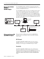
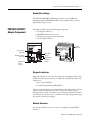
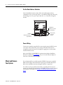

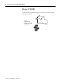
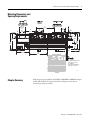

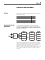
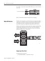
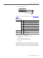
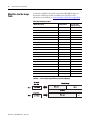
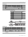

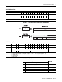
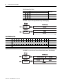
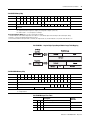

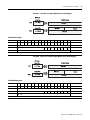
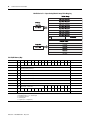


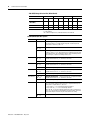
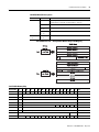
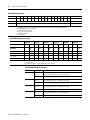
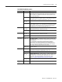
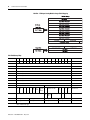
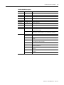
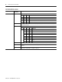
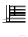
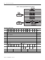
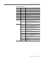


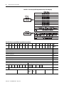
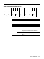
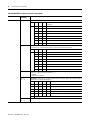
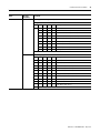


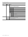
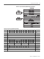
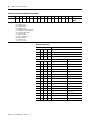

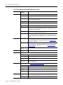

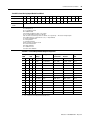


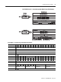
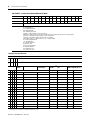


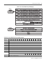

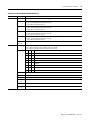


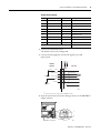
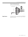


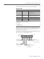


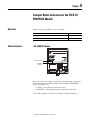


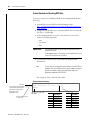

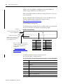


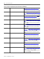
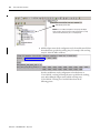


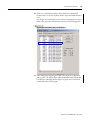


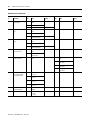
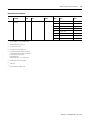


![EX MV MX3 User Manual [May16].vp](http://vs1.manualzilla.com/store/data/005646159_1-0d378a1c318c2dc00419aef6af60da73-150x150.png)