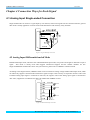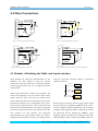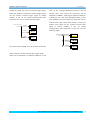
1
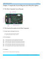
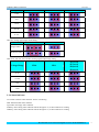
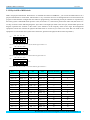
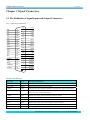
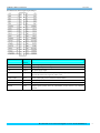
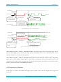
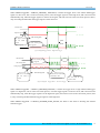
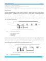
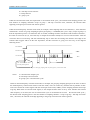
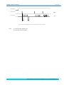
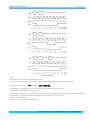
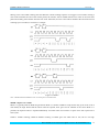
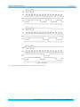
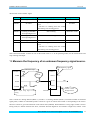
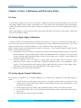
USB2815
User’s Manual
Beijing ART Technology Development Co., Ltd.
USB2815 Data Acquisition
V6.1.18
Contents
Contents ................................................................................................................................................................................2
Chapter 1 Overview ..............................................................................................................................................................3
Chapter 2 Components Layout Diagram and a Brief Description .......................................................................................5
2.1 The Main Component Layout Diagram ..................................................................................................................5
2.2 The Function Description for the Main Component ...............................................................................................5
2.2.1 Signal Input and Output Connectors ............................................................................................................5
2.2.2 Potentiometer ...............................................................................................................................................5
2.2.3 Jumper..........................................................................................................................................................5
2.2.4 Status indicator.............................................................................................................................................6
2.2.5 Physical ID of DIP Switch ...........................................................................................................................7
Chapter 3 Signal Connectors................................................................................................................................................8
3.1 The Definition of Signal Input and Output Connectors ..........................................................................................8
Chapter 4 Connection Ways for Each Signal......................................................................................................................10
4.1 Analog Input Single-ended Connection ................................................................................................................10
4.2 Analog Input Differential-ended Mode .................................................................................................................10
4.2 Other Connections.................................................................................................................................................11
4.3 Methods of Realizing the Multi-card Synchronization .........................................................................................11
Chapter 5 The Instruction of the AD Trigger Function.......................................................................................................13
5.1 AD Internal Trigger Mode.....................................................................................................................................13
5.2 AD External Trigger Mode....................................................................................................................................13
5.2.1 Edge Trigger Function................................................................................................................................13
5.2.2 Triggering Level Function..........................................................................................................................14
Chapter 6 Methods of using AD Internal and External Clock Function.............................................................................16
6.1 Internal Clock Function of AD..............................................................................................................................16
6.2 External Clock Function of AD.............................................................................................................................16
6.3 Methods of Using AD Continuum and Grouping Sampling Function ..................................................................16
6.3.1 AD Continuum Sampling Function............................................................................................................16
6.3.2 AD Grouping Sampling Function ..............................................................................................................17
Chapter 7 Methods of using Timer/Counter 8254...............................................................................................................21
7.1 The working mode ................................................................................................................................................21
7.2 Measure the frequency of an unknown frequency signal source. .........................................................................29
Chapter 8 Notes, Calibration and Warranty Policy............................................................................................................31
8.1 Notes .....................................................................................................................................................................31
8.2 Analog Signal Input Calibration............................................................................................................................31
8.3 Analog Signal Output Calibration.........................................................................................................................31
8.4 Analog output use..................................................................................................................................................32
8.5 Warranty Policy.....................................................................................................................................................32
Products Rapid Installation and Self-check ........................................................................................................................33
Rapid Installation ........................................................................................................................................................33
Self-check ...................................................................................................................................................................33
Delete Wrong Installation ...........................................................................................................................................33
BUY ONLINE at art-control.com/englishs or CALL +86-10-51289836(CN)
2
USB2815 Data Acquisition
V6.1.18
Chapter 1 Overview
In the fields of Real-time Signal Processing, Digital Image Processing and others, high-speed and high-precision data
acquisition modules are demanded. ART USB2815 data acquisition module, which brings in advantages of similar
products that produced in china and other countries, is convenient for use, high cost and stable performance.
ART USB2815 is a data acquisition module based on USB bus. It can be directly inserted into USB interface to
constitute the laboratory, product quality testing center and systems for different areas of data acquisition, waveform
analysis and processing. It may also constitute the monitoring system for industrial production process.
Unpacking Checklist
Check the shipping carton for any damage. If the shipping carton and contents are damaged, notify the local dealer or
sales for a replacement. Retain the shipping carton and packing material for inspection by the dealer.
Check for the following items in the package. If there are any missing items, contact your local dealer or sales.
¾ USB2815 Data Acquisition Board
¾ ART Disk
a) user’s manual (pdf)
b) drive
c) catalog
¾ Warranty Card
FEATURES
AD analog input
¾
¾
¾
¾
¾
¾
¾
¾
¾
¾
¾
¾
¾
¾
¾
¾
¾
¾
¾
Input Range: ±10V, ±5V, ±2.5, 0~10V, 0~5V
16-bit resolution
Sampling Rate: maximum 250KHz
Analog Input Mode: 16SE/8DI
Data Read Mode: non-empty, half-full inquiry mode
Memory Depth: 8K word FIFO memory
Memory Signs: non-empty, half-full and overflow
AD Mode: continuum sampling , grouping sampling
Group Interval: software-configurable, minimum value is sampling period, maximum value is 419430uS
Loops of Group: software-configurable, minimum value is one time , maximum value is 255 times
Clock Source: external clock, internal clock( software-configurable)
Trigger Mode: software trigger, hardware trigger(external trigger)
Trigger Type: level trigger , edge trigger
Trigger Direction: negative, positive, either positive or negative trigger
Trigger Source: ATR, DTR
Analog Trigger Source (ATR)Input Range: ±10V
Digital Trigger Source (DTR) Input Range: standard TTL level
AD Conversion Time: 1.25uS
Programmable Gain: 1, 2, 4, 8 (AD8251 default)or 1, 2, 5, 10 (AD8250) or 1, 10, 100, 1000 (AD8253)
BUY ONLINE at art-control.com/englishs or CALL +86-10-51289836(CN)
3
USB2815 Data Acquisition
¾
¾
¾
¾
¾
¾
V6.1.18
Analog Input Impedance: 10MΩ
Amplifier Set-up Time: 785nS(0.001%)(max)
Non-linear error: ±3LSB(Maximum)
System Measurement Accuracy: 0.01%
Operating Temperature Range: 0℃~55℃
Storage Temperature Range: -20℃~70℃
DA analog output
¾
¾
¾
¾
¾
¾
¾
¾
Output Range: ±10V,±5V, 0~10V, 0~5V
12-bit resolution
Set-up Time: 10μS (0.01%)
Channel No.: 4-channel
Non-linear error: ±1LSB(Maximum)
Output Error (full-scale): ±1LSB
Operating Temperature Range: 0℃~55℃
Storage Temperature Range: -20℃~+70℃
DI digital input
¾
¾
¾
¾
Channel No.: 8-channel
Electric Standard: CMOS compatible
High Voltage: ≧3.5V
Low Voltage: ≦1.5V
DO digital output
¾
¾
¾
¾
Channel No.: 8-channel
Electrical Standard: CMOS compatible
High Voltage: ≧4.45V
Low Voltage: ≦0.5V
Counter/timer
¾
¾
¾
¾
¾
¾
¾
¾
Counter No.: 3 separate counter
Counter mode: subtractive counter
Number of digits of the counter: 16-bit
Operate Type: 4 operate type (software-configurable)
Counting Mode: 6 counting mode(software-configurable)
Counting Type: binary counting and BCD code counting
Input Electric Standard: High Level≧2.2V, Low Level≦0.8V
Output Electric Standard: High Level≧3.0V, Low Level≦0.4V
BUY ONLINE at art-control.com/englishs or CALL +86-10-51289836(CN)
4
USB2815 Data Acquisition
V6.1.18
Chapter 2 Components Layout Diagram and a Brief Description
2.1 The Main Component Layout Diagram
2.2 The Function Description for the Main Component
2.2.1 Signal Input and Output Connectors
CN1: analog signal input and output connector
P1: digital signal input and output connector
2.2.2 Potentiometer
RP1:
RP2:
RP3:
RP4:
RP5:
RP6:
RP7:
Analog signal input zero-point adjustment potentiometer
Analog signal input full-scale adjustment potentiometer
DA0 analog signal output full-scale adjustment potentiometer
DA1 analog signal output full-scale adjustment potentiometer
DA2 analog signal output full-scale adjustment potentiometer
DA3 analog signal output full-scale adjustment potentiometer
DA analog signal output zero-point adjustment potentiometer
2.2.3 Jumper
JP1, JP2, and JP3: Analog signal input range setting
BUY ONLINE at art-control.com/englishs or CALL +86-10-51289836(CN)
5
USB2815 Data Acquisition
Voltage Range
V6.1.18
JP1
JP2
JP3
±10V
±5V
±2.5V
0~10V
0~5V
JP4, JP5: Analog signal input mode setting
Input mode
JP4
JP5
Single-ended
Different-ended
JP10, JP11, JP6, JP7, JP8, and JP9: Analog signal output range setting
Voltage Range
JP10
JP11
JP6(AO0)
JP7(AO1)
JP8(AO2)
JP9(AO3)
0~5V
0~10V
±5V
±10V
2.2.4 Status indicator
Ovr: FIFO overflow status indicator. On for overflowing.
Half: FIFO half-full status indicator.
Npt: FIFO non-empty status indicator
DABusy: DA working status indicator. When the light is on, it shows that DA is working.
ADBusy: AD working status indicator. When the light is on, it shows that AD is working.
BUY ONLINE at art-control.com/englishs or CALL +86-10-51289836(CN)
6
USB2815 Data Acquisition
V6.1.18
2.2.5 Physical ID of DIP Switch
DID1: Set physical ID number. When the PC is installed more than one USB2815 , you can use the DIP switch to set a
physical ID number for each board, which makes it very convenient for users to distinguish and visit each board in the
progress of the hardware configuration and software programming. The following four-byte numbers are expressed by
the binary system: When DIP switch points to "ON", that means "1", and when it points to the other side, that means "0."
As they are shown in the following diagrams: byte "ID3" is the high byte."ID0" is the low byte, and the black part in the
diagram represents the location of the switch. (Test softwares of the company often use the logic ID management
equipments and at this moment the physical ID DIP switch is invalid. If you want to use more than one kind of the
equipments in one and the same system at the same time, please use the physical ID as much as possible.).
ON
ID3 ID2 ID1 ID0
ON
DID1
1
2
3
4
The above chart shows"1111", so it means that the physical ID is 15.
ON
ID3 ID2 ID1 ID0
ON
DID1
1
2
3
4
The above chart shows"0111", so it means that the physical ID is 7.
ON
ID3 ID2 ID1 ID0
ON
DID1
1
2
3
4
The above chart shows"0101", so it means that the physical ID is 5.
ID3
OFF(0)
ID2
OFF(0)
ID1
OFF(0)
ID0
OFF(0)
0
0
OFF(0)
OFF(0)
OFF(0)
ON(1)
1
1
OFF(0)
OFF(0)
ON(1)
OFF(0)
2
2
OFF(0)
OFF(0)
ON(1)
3
3
OFF(0)
OFF(0)
4
4
OFF(0)
ON(1)
ON(1)
ON(1)
OFF(0)
5
ON(1)
ON(1)
OFF(0)
5
OFF(0)
OFF(0)
ON(1)
6
6
OFF(0)
ON(1)
ON(1)
7
7
ON(1)
OFF(0)
OFF(0)
ON(1)
OFF(0)
8
8
ON(1)
OFF(0)
OFF(0)
9
9
ON(1)
OFF(0)
ON(1)
A
10
ON(1)
OFF(0)
ON(1)
B
11
ON(1)
ON(1)
OFF(0)
C
12
ON(1)
ON(1)
OFF(0)
D
13
ON(1)
ON(1)
ON(1)
ON(1)
OFF(0)
E
14
ON(1)
ON(1)
ON(1)
ON(1)
F
15
ON(1)
OFF(0)
ON(1)
OFF(0)
Physical ID(Hex) Physical ID(Dec)
BUY ONLINE at art-control.com/englishs or CALL +86-10-51289836(CN)
7
USB2815 Data Acquisition
V6.1.18
Chapter 3 Signal Connectors
3.1 The Definition of Signal Input and Output Connectors
CN1: 37-pin D-type definition
AI1
37
AI3
36
AI5
35
AI7
34
AI9
33
AI11
32
AI13
31
AI15
30
AGND
AO1
29
AO3
NC
27
26
NC
25
AGND
24
+5V
23
DTR
22
CLKOUT
21
CLKIN
20
28
19
AI0
18
AI2
17
AI4
16
AI6
15
AI8
14
AI10
13
AI12
12
11
AI14
AGND
10
AO0
9
AO2
8
NC
7
NC
6
ATR
5
AGND
4
DGND
3
DGND
2
DGND
1
DGND
Pin definition about AD:
Pin name
Type
Pin function definition
AI0~AI15
Input
Analog input, reference ground is AGND.
AO0~AO3
Output
Analog output, reference ground is AGND.
AGND
GND
Analog ground. This AGND pin should be connected to the system’s AGND plane.
DGND
GND
Digital ground. Ground reference for Digital circuitry. This DGND pin should be
connected to the system’s DGND plane.
CLKIN
Input
External clock input, please use DGND as reference ground.
CLKOUT
Output
Internal clock output
ATR
Input
Analog trigger signal input, choose AGND as reference ground.
DTR
Input
Digital trigger signal input, choose DGND as reference ground.
+5V
Output
5V power supply output.
NC
Not connected
BUY ONLINE at art-control.com/englishs or CALL +86-10-51289836(CN)
8
USB2815 Data Acquisition
V6.1.18
Pin definition about Digital Input/Output
Pin name
Pin
Pin function definition
feature
DI0~DI7
Input
Digital signal input, reference ground is DGND.
DO0~DO7
Output
Digital signal output, reference ground is DGND.
+5V
Output
5V power supply output..
CLK2M
Output
On-board 2MHz clock oscillator pulse output, Output cycle 0.5 microseconds,
provides the clock source signal for CLK0~CLK2
CLK0~CLK2
Input
Clock / pulse input pins for 3 channels of 8254 counters.
GATE0~GATE2
Input
Gate input pins for 3 channels of 8254 counters
OUT0~OUT2
Output
Output pins of 3 channels of 8254 counters
DGND
GND
Digital signals ground, when use counter/timer we best choose it as reference
ground.
BUY ONLINE at art-control.com/englishs or CALL +86-10-51289836(CN)
9
USB2815 Data Acquisition
V6.1.18
Chapter 4 Connection Ways for Each Signal
4.1 Analog Input Single-ended Connection
Single-ended mode can achieve a signal input by one channel, and several signals use the common reference ground.
This mode is widely applied in occasions of the small interference and relatively many channels.
Figure 4.1 single-ended input connection
4.2 Analog Input Differential-ended Mode
Double-ended input mode, which was also called differential input mode, uses positive and negative channels to input a
signal. This mode is mostly used when biggish interference happens and the channel numbers are few.
Single-ended/double-ended mode can be set by the software, please refer to USB2815 software manual.
According to the diagram below, USB2815 board can be connected as analog voltage double-ended input mode, which
can effectively suppress common-mode interference signal to improve the accuracy of acquisition. Positive side of the
8-channel analog input signal is connected to AI0~AI7, the negative side of the analog input signal is connected to
AI8~AI15, equipments in industrial sites share the AGND with USB2815 board.
Figure 4.2 double-ended input connection
BUY ONLINE at art-control.com/englishs or CALL +86-10-51289836(CN)
10
USB2815 Data Acquisition
V6.1.18
4.2 Other Connections
Figure 4.3 analog signal output connection
Figure 4.5 digital signal output connection
Figure 4.4 digital signal input connection
Figure 4.6 Clock Input/Output and Trigger Signal Connection
4.3 Methods of Realizing the Multi-card Synchronization
Three methods can realize the synchronization for the
USB2815, the first method is using the cascade
master-slave card, the second one is using the common
external trigger, and the last one is using the common
external clock.
using the multi-card cascaded model to expand the
number of channels.
CLKOUT
CLKIN
When using master-slave cascade card programs, the
master card generally uses the internal clock source
model, while the slave card uses the external clock
source mode. After the master card and the slave card are
initialized according to the corresponding clock source
mode. At first, start all the slave cards, as the main card
has not been activated and there is no output clock signal,
so the slave card enters the wait state until the main card
was activated. At this moment, the multi-card
synchronization has been realized. When you need to
sample more than channels of a card, you could consider
CLKIN
Master Card
Slave Card 1
Slave Card 2
When using the common external trigger, please make
sure all parameters of different USB2815 are the same.
At first, configure hardware parameters, and use analog
or digital signal triggering (ATR or DTR), then connect
the signal that will be sampled by USB2815, input
triggering signal from ART pin or DTR pin, then click
“Start Sampling” button, at this time, USB2815 does not
BUY ONLINE at art-control.com/englishs or CALL +86-10-51289836(CN)
11
USB2815 Data Acquisition
V6.1.18
sample any signal but waits for external trigger signal.
When each module is waiting for external trigger signal,
use the common external trigger signal to startup
modules, at last, we can realize synchronization data
acquisition in this way. See the following figure:
External Trigger Signal ATR/DTR
ATR/DTR
ATR/DTR
USB 2815
USB 2815
same. At first, configure hardware parameters, and use
external clock, then connect the signal that will be
sampled by USB2815, input trigger signal from ART pin
or DTR pin, then click “Start Sampling” button, at this
time, USB2815 does not sample any signal, but wait for
external clock signal. When each module is waiting for
external clock signal, use the common external clock
signal to startup modules, at last, we realize
synchronization data acquisition in this way. See the
following figure:
USB 2815
Note:when using the DTR, select the internal clock mode
When using the common external clock trigger, please
make sure all parameters of different USB2815 are the
BUY ONLINE at art-control.com/englishs or CALL +86-10-51289836(CN)
12
USB2815 Data Acquisition
V6.1.18
Chapter 5 The Instruction of the AD Trigger Function
5.1 AD Internal Trigger Mode
When AD is in the initialization, if the AD hardware parameter ADPara.TriggerMode = USB2815_TRIGMODE_SOFT,
we can achieve the internal trigger acquisition. In this function, when calling the StartDeviceProAD function, it will
generate AD start pulse, AD immediately access to the conversion process and not wait for the conditions of any other
external hardware. It also can be interpreted as the software trigger.
As for the specific process, please see the figure below, the cycle of the AD work pulse is decided by the sampling
frequency.
Start Enable
Convert Pulse
The first working
pulse after the AD
start pulse
Figure 5.1 Internal Trigger Mode
5.2 AD External Trigger Mode
When AD is in the initialization, if the AD hardware parameter ADPara.TriggerMode = USB2815_TRIGMODE_POST,
we can achieve the external trigger acquisition. In this function, when calling the StartDeviceProAD function, AD will
not immediately access to the conversion process but wait for the external trigger source signals accord with the
condition, then start converting the data. It also can be interpreted as the hardware trigger. Trigger source includes the
DTR (Digital Trigger Source) and ATR (Analog Trigger Source)
The trigger modes include the edge trigger and level trigger.
5.2.1 Edge Trigger Function
Edge trigger is to capture the characteristics of the changes between the trigger source signal and the trigger level signal
to trigger AD conversion.
When ADPara.TriggerDir = USB2815_TRIGDIR_NEGATIVE, choose the trigger mode as the falling edge trigger.
That is, when the DTR trigger signal is on the falling edge, AD will immediately access to the conversion process, and
its follow-up changes have no effect on AD acquisition.
BUY ONLINE at art-control.com/englishs or CALL +86-10-51289836(CN)
13
USB2815 Data Acquisition
V6.1.18
AD Start Pulse
Digital Trigger Signal
The falling edge before
The waiting time
The first falling edge after the
the AD started is invalid
AD started is valid
The
first
working
pulse after triggered
AD Working Pulse
Figure5.2 Digital Trigger Source,Falling edge Trigger
AD Start Pulse
The first working
pulse after triggered
AD Working Pulse
Trigger Level
Analog Trigger Signal
The waiting time
The falling edge before
The first falling edge after the
the
AD started is valid
AD
started
is
invalid
Figure5.3 Analog Trigger Source,Falling edge Trigger
When ADPara.TriggerDir = USB2815_TRIGDIR_POSITIVE, choose the trigger mode as rising edge trigger. That is,
when the DTR trigger signal is on the rising edge, AD will immediately access to the conversion process, and its
follow-up changes have no effect on AD acquisition.
When ADPara.TriggerDir = USB2815_TRIGDIR_POSIT_NEGAT, choose the trigger mode as rising or falling edge
trigger. That is, when the DTR trigger signal is on the rising or falling edge, AD will immediately access to the
conversion process, and its follow-up changes have no effect on AD acquisition. This function can be used in the case
that the acquisition will occur if the exoteric signal changes.
5.2.2 Triggering Level Function
Level trigger is to capture the condition that trigger signal is higher or lower than the trigger level to trigger AD
conversion.
BUY ONLINE at art-control.com/englishs or CALL +86-10-51289836(CN)
14
USB2815 Data Acquisition
V6.1.18
When ADPara.TriggerDir = USB2815_TRIGDIR_ NEGATIVE, it means the trigger level is low. When DTR trigger
signal is in low level, AD is in the conversion process, once the trigger signal is in the high level, AD conversion will
automatically stop, when the trigger signal is in the low level again, AD will re-access to the conversion process, that is,
only converting the data when the trigger signal is in the low level.
AD Start Pulse
Digital Trigger Signal
The waiting time
The high level before
the
AD
started
is
pause
The first working pulse
invalid
AD Working Pulse
mode
after triggered
Figure5.4 Digital Trigger Source,High Level Trigger
AD Start Pulse
AD Working Pulse
The first working pulse
pause
after triggered
mode
Trigger Level
Analog Trigger Signal
The waiting time
The low level before
The first low level after the
the
AD started is valid
AD
started
is
invalid
Low level after the AD
started is valid
Figure5.4 Digital Trigger Source,Low Level Trigger
When ADPara.TriggerDir = USB2815_TRIGDIR_POSITIVE, it means the trigger level is high. When DTR trigger
signal is in high level, AD is in the conversion process, once the trigger signal is in the low level, AD conversion will
automatically stop, when the trigger signal is in the high level again, AD will re-access to the conversion process, that
is, only converting the data when the trigger signal is in the high level.
When ADPara.TriggerDir = USB2815_TRIGDIR_POSIT_NEGAT, the effect is the same as choosing the internal
software trigger.
BUY ONLINE at art-control.com/englishs or CALL +86-10-51289836(CN)
15
USB2815 Data Acquisition
V6.1.18
Chapter 6 Methods of using AD Internal and External Clock
Function
6.1 Internal Clock Function of AD
Internal Clock Function refers to the use of on-board clock oscillator and the clock signals which are produced by the
user-specified frequency to trigger the AD conversion regularly. To use the clock function, the hardware parameters
ADPara.ClockSource = USB2815 _CLOCKSRC_IN should be installed in the software. The frequency of the clock in
the software depends on the hardware parameters ADPara.Frequency. For example, if Frequency = 100000, that means
AD work frequency is 100000Hz (that is, 100 KHz, 10μs /point).
6.2 External Clock Function of AD
External Clock Function refers to the use of the outside clock signals to trigger the AD conversion regularly. The clock
signals are provide by the CLKIN pin of the CN1 connector.
The outside clock can be provided by USB2815 clock
output (CLKOUT of CN1), as well as other equipments, for example clock frequency generators. To use the external
clock function, the hardware parameters ADPara.ClockSource = USB2815_CLOCKSRC_OUT should be installed in
the software. The clock frequency depends on the frequency of the external clock, and the clock frequency on-board
(that is, the frequency depends on the hardware parameters ADPara.Frequency) only functions in the packet acquisition
mode and its sampling frequency of the AD is fully controlled by the external clock frequency.
6.3 Methods of Using AD Continuum and Grouping Sampling Function
6.3.1 AD Continuum Sampling Function
The continuous acquisition function means the sampling periods for every two data points are completely equal in the
sampling process of AD, that is, completely uniform speed acquisition, without any pause, so we call that continuous
acquisition.
To use the continuous acquisition function, the hardware
parameters ADPara.ADMode = USB2815
_ADMODE_SEQUENCE should be installed in the software. For example, in the internal clock mode, hardware
parameters ADPara.Frequency = 100000 (100KHz) should be installed, and 10 microseconds after the AD converts the
first data point, the second data point conversion starts, and then 10 microseconds later the third data point begins to
convert, and so on.
BUY ONLINE at art-control.com/englishs or CALL +86-10-51289836(CN)
16
USB2815 Data Acquisition
V6.1.18
6.3.2 AD Grouping Sampling Function
Grouping acquisition (pseudo-synchronous acquisition) function refers to the sampling clock frequency conversion
among the channels of the group in the AD sampling process, and also a certain waiting time exists between every two
groups, this period of time is known as the Group Interval. Loops of group refer to numbers of the cycle acquisition for
each channel in the same group. In the internal clock mode and the fixed-frequency external clock mode, the time
between the groups is known as group cycle. The conversion process of this acquisition mode as follows: a short time
stop after the channels conversion in the group (that is, Group Interval), and then converting the next group, followed
by repeated operations in order, so we call it grouping acquisition.
The purpose of the application of the grouping acquisition is that: at a relatively slow frequency, to ensure that all of the
time difference between channels to become smaller in order to make the phase difference become smaller, thus to
ensure the synchronization of the channels, so we also say it is the pseudo-synchronous acquisition function. In a group,
the higher the sampling frequency is, the longer Group Interval is, and the better the relative synchronization signal is.
The sampling frequency in a group depends on ADPara. Frequency, Loops of group depends on
ADPara.LoopsOfGroup, the Group Interval depend on ADPara. Group Interval.
Based on the grouping function, it can be divided into the internal clock mode and the external clock mode. Under the
internal clock mode, the group cycle is decided by the internal clock sampling period, the total number of sampling
channels, Loops of group and Group Interval together. In each cycle of a group, AD only collects a set of data. Under
the external clock mode, external clock cycle ≥ internal clock sampling cycle × the total number of sampling
channels
× Loops of group + AD chip conversion time, AD data acquisition is controlled and triggered by external
clock. The external clock mode is divided into fixed frequency external clock mode and unfixed frequency external
clock mode. Under the fixed frequency external clock mode, the group cycle is the sampling period of the external
clock.
The formula for calculating the external signal frequency is as follows:
Under the internal clock mode:
Group Cycle = the internal clock sampling period × the total number of sample channels × Loops of group + AD chips
conversion time + Group Interval
External signal cycle = (cycle signal points / Loops of group) × Group Cycle
External signal frequency = 1 / external signal cycle
Under the external clock mode: (a fixed-frequency external clock)
Group Cycle = external clock cycle
External signal cycle = (cycle signal points / Loops of group) × Group Cycle
External signal frequency = 1 / external signal cycle
Formula Notes:
The internal sampling clock cycle = 1 / (AD Para. Frequency)
The total number of sampling channels = AD Para. Last Channel – AD Para. First Channel + 1
BUY ONLINE at art-control.com/englishs or CALL +86-10-51289836(CN)
17
USB2815 Data Acquisition
V6.1.18
Loops of group == ADPara.LoopsOfGroup
AD Chips conversion time = see "AD Analog Input Function" parameter
Group Interval = AD Para. Group Interval
Signal Cycle Points = with the display of the waveform signal in test procedures, we can use the mouse to measure the
signal cycle points.
Under the internal clock mode, for example, sample two-channel 0, 1, and then 0 and 1 become a group. Sampling
frequency (Frequency) = 100000Hz (cycle is 10μs), Loops of group is 1, Group Interval = 50μs, then the acquisition
process is to collect a set of data first, including a data of channel 0 and a data of channel 1. We need 10uS to sample
the two data, 20μs to convert the data from the two channels. After the conversion time of an AD chip, AD will
automatically cut-off to enter into the waiting state until the 50μs group interval ends. We start the next group, begin to
convert the data of channel 0 and 1, and then enter into the waiting state again, and the conversion is going on in this
way, as the diagram following shows:
Start Enabled
Convert Pulse
a
b
c
a
d
Figure 6.1 Grouping Sampling which grouping cycle No is 1 under the Internal Clock Mode
Note:
a― internal clock sample cycle
b― AD chips conversion time
c―Group Interval
d― group cycle
Change the loops of group into 2, then the acquisition process is to collect the first set of data, including two data of
channel 0 and two data of channel 1, the conversion order is 0,1,0,1. We need 10μs to sample each of the four data.
After the conversion time of an AD chip, AD will automatically stop to enter into the waiting state until the 50μs Group
Interval ends. We start the next group, begin to convert the data of channel 0 and 1, and then enter into the waiting state
again, and the conversion is going on in this way, as the diagram following shows:
Start Enabled
Convert Pulse
b
a
c
a
d
Figure 6.2 Grouping Sampling which grouping cycle No is 2 under the Internal Clock Mode
Notes:
a― internal clock sample cycle
BUY ONLINE at art-control.com/englishs or CALL +86-10-51289836(CN)
18
USB2815 Data Acquisition
V6.1.18
b― AD chips conversion time
c―Group Interval
d― group cycle
Under the external clock mode, the requirement is: the external clock cycle ≥ the internal clock sampling period × the
total number of sampling channels× Loops of group + AD chip conversion time, otherwise, the external clock
appearing in the group conversion time will be ignored.
Under the fixed-frequency external clock mode, for example, when sampling data of two-channel 0, 1, then channel 0
and channel 1 consist of a group. Sampling frequency (Frequency) = 100000Hz (the cycle is 10μs), Loops of group is 2,
then the acquisition process is to collect the first set of data, including two data of channel 0 and two data of channel 1,
the order of conversion 0,1,0,1, We need 10μs to sample the four data and 40μs to convert of the four data. After the
conversion time of an AD chip, AD will automatically stop to enter into the waiting state until the next edge of the
external clock triggers AD to do the next acquisition, and the conversion is going on in this way, as the diagram
following shows:
Start Enabled
External Clock
Convert Pulse
a
b
d
The external clock before
the start pulse is ignored
Figure 6.3 Grouping sampling under the fixed frequency external clock mode
Notes:
a― internal clock sample cycle
b―AD chips conversion time
d―group cycle(external clock cycle)
Under an unfixed-frequency external clock mode, for example, the grouping sampling principle is the same as that of
the fixed-frequency external clock mode. Under this mode, users can control any channel and any number of data.
Users will connect the control signals with the clock input of the card (CLKIN), set the sampling channels and Loops
of group. When there are external clock signals, it will sample the data which is set by users. Because the external
clock frequency is not fixed, the size of external clock cycle is inconsistent but to meet:
the external clock cycle ≥
the internal clock sampling period × the total number of sampling channels × Loops of group + AD chip conversion
time, , otherwise, the external clock edge appearing in the group conversion time will be ignored.
BUY ONLINE at art-control.com/englishs or CALL +86-10-51289836(CN)
19
USB2815 Data Acquisition
V6.1.18
Start Enabled
External Clock
Convert Pulse
a
b
Figure 6.4 Grouping sampling under the not fixed frequency external clock mode
Note:
a― internal clock sample cycle
b―AD chips conversion time
BUY ONLINE at art-control.com/englishs or CALL +86-10-51289836(CN)
20
USB2815 Data Acquisition
V6.1.18
Chapter 7 Methods of using Timer/Counter 8254
7.1 The working mode
MODE 0 Interrupt on terminal count
Mode 0 is typically used for event counting. After the Control Word is written, OUT is initially low, and will remain
low until the Counter reaches zero. OUT then goes high and remains high until a new count or a new Mode 0 Control
Word is written into the Counter.
GATE=1 enables counting; GATE=0 disables counting. GATE has no effect on OUT.
After the Control Word and initial count are written to a Counter, the initial count will be loaded on the next CLK pulse.
This CLK pulse does not decrement the count, so for an initial count of N, OUT does not go high until N+1 CLK
pulses after the initial count is written.
If a new count is written to the Counter, it will be loaded on the next CLK pulse and counting will continue from the
new count. If a two-byte count is written, the following happens:
1) Writing the first byte disables counting. OUT is set low immediately (no clock pulse required)
2) Writing the second byte allows the new count to be loaded on the next CLK pulse
This allows the counting sequence to be synchronized by software. Again, OUT does not go high until N+1 CLK pulses
after the new count of N is written.
If an initial count is written while GATE=0, it will still be loaded on the next CLK pulse. When GATE goes high, OUT
will go high N CLK pulse later, no CLK pulse is needed to load the Counter as this has already been done.
MODE 1 Hardware retriggerable one-shot
OUT will be initially high. OUT will go low on the CLK pulse following a trigger to begin the one-shot pulse, and will
remain low until the Counter reaches zero.
OUT will then go high and remain high until the CLK pulse after the next trigger.
After writing the Control Word and initial count, the Counter is armed. A trigger results in loading the Counter and
setting OUT low on the next CLK pulse, thus starting the one-shot pulse. An initial count of N will result in a one-shot
pulse N CLK cycles in duration. The one-shout is retriggerable, hence OUT will remain low for N CLK pulses after
any trigger. The one-shot pulse can be repeated without rewriting the same count into the counter. GATE has no effect
on OUT.
If a new count is written to the Counter during a one-shot pulse, the current one-shot is not affected unless the counter
is retriggered. In that case, the Counter is loaded with the new count and the one-shot pulse continues until the new
count expires.
BUY ONLINE at art-control.com/englishs or CALL +86-10-51289836(CN)
21
USB2815 Data Acquisition
V6.1.18
Figure 7.1 Mode 0
NOTE
The following conventions apply to all mode timing diagrams
1. Counters are programmed for binary (not BCD) counting and for reading/writing least significant byte (LSB) only.
2. The counter is always selected ( CS always low) 错误!未指定书签。
3. CW stands for “Control Word”; CW=10 means a control word of 10 HEX is written to the counter.
4. LSB stands for “Least Significant Byte” of count.
5. Numbers below diagrams are count values. The lower number is the least significant byte. The upper number is the most significant byte.
Since the counter is programmed to read/writer LSB only, the most significant byte cannot be read.
N stands for an undefined count.
Vertical lines show transitions between count values.
BUY ONLINE at art-control.com/englishs or CALL +86-10-51289836(CN)
22
USB2815 Data Acquisition
V6.1.18
Figure 7.2 Mode 1
MODE 2 Rate Generator
This Mode functions like a divide-by-N counter. It is typically used to generate a Real Time Clock interrupt. OUT will
initially be high. When the initial count has decremented to 1, OUT goes low for on CLK pulse. OUT then goes high
again, the Counter reloads the initial count and the process is repeated. Mode 2 is periodic; the same sequence is
repeated indefinitely. For an initial count of N, the sequence repeats every N CLK cycles.
GATE=1 enables counting; GATE=0 disables counting. If GATE goes low during an output pulse, OUT is set high
immediately. A trigger reloads the Counter with the initial count on the next CLK pulse; OUT goes low N CLK pulses
after the trigger. Thus the GATE input can be used to synchronize the Counter.
After writing a Control Word and initial count, the Counter will be loaded on the next CLK pulse. OUT goes low N
CLK Pulses after the initial count is written. This allows the Counter to be synchronized by software also.
BUY ONLINE at art-control.com/englishs or CALL +86-10-51289836(CN)
23
USB2815 Data Acquisition
V6.1.18
Writing a new count while counting does not affect the current counting sequence. If a trigger is received after writing a
new count but before the end of the current period, the Counter will be loaded with the new count on the next CLK
pulse and counting will continue from the new count. Otherwise, the new count will be loaded at the end of the current
counting cycle. In mode2, a COUNT of 1 I illegal.
Figure 7.3 Mode 2
Note: A GATE transition should not occur one clock prior to terminal count.
MODE 3 Square wave mode
Mode 3 is typically used for Baud rate generation. Mode 3 is similar to Mode 2 except for the duty cycle of OUT. OUT
will initially be high. When half the initial count has expired, OUT goes low for mainder of the count. Mode 3 is
periodic; the sequence above is repeated indefinitely. An initial count of N results in a square wave with a period of N
CLK cycles.
GATE=1 enables counting; GATE=0 disables counting. If GATE goes low while OUT is low, OUT is set high
BUY ONLINE at art-control.com/englishs or CALL +86-10-51289836(CN)
24
USB2815 Data Acquisition
V6.1.18
immediately; no CLK pulse is required. A trigger reloads the Counter with the initial count on the next CLK pulse.
Thus the GATE input can be used to synchronize the Counter
After writing a Control Word and initial count, the Counter will be loaded on the next CLK pulse. This allows the
Counter to be synchronized by software also.
Writing a new count while counting does not affect the current counting sequence. If a trigger is received after writing a
new count but before the end of the current half-cycle of the square wave, the Counter will be loaded with the new
count on the next CLK pulse and counting will continue from the new count. Otherwise, the new counter will be loaded
at the end of the current half-cycle.
Mode 3 is implemented as follows:
Even counts: OUT is initially high. The initial count is loaded on one CLK pulse and then is decremented by two on
succeeding CLK pulses. When the count expires OUT changes value and the Counter is reloaded with the initial count.
The above process is repeated indefinitely.
Odd counts: OUT is initially high. The initial count minus one (an even number) is loaded on one CLK pulse and then
is decremented by two on succeeding CLK pulses. One CLK pulse after the count expires. OUT goes low and the
Counter is reloaded with the initial count minus one. Succeeding CLK pulses decrement the count by two. When the
count expires, OUT goes high again and the Counter is reloaded with the initial count minus one. The above process is
repeated indefinitely. So for odd counts, OUT will be high for (N+1)/2 counts and low for (N-1)/2 counts.
MODE 4 Software triggered strobe
OUT will be initially high. When the initial count expires, OUT will go low for one CLK pulse and then go high again.
The counting sequence is “triggered” by writing the initial count.
GATE=1 enables counting; GATE=0 disables counting. GATE has no effect on OUT.
After writing a Control Word and initial count, the Counter will be loaded on the next CLK pulse. This CLK pulse does
not decrement the count, so for an initial count of N, OUT does not strobe low until N+1 CLK pulses after the initial
count is written.
If a new count is written during counting, if will be loaded on the next CLK pulse and counting will continue from the
new count. If a two-byte count is written, the following happens:
1) Writing the first byte has no effect on counting.
2) Writing the second byte allows the new count to be loaded on the next CLK pulse.
This allows the sequence to be ‘‘retriggered’ by software. OUT strobe low N+1 CLK pulses after
the new count of N is written.
BUY ONLINE at art-control.com/englishs or CALL +86-10-51289836(CN)
25
USB2815 Data Acquisition
V6.1.18
Figure 7.4 Mode 3
Note: A GATE transition should not occur one clock prior to terminal count.
BUY ONLINE at art-control.com/englishs or CALL +86-10-51289836(CN)
26
USB2815 Data Acquisition
V6.1.18
Figure 7.5 Mode 4
MODE 5 Hardware triggered strobe
OUT will initially be high. Counting is triggered by a rising edge of GATE. When the initial count has expired, OUT
will go low for one CLK pulse and then go high again.
After writing the Control Word and initial count, the counter will not be loaded until the CLK pulse after a trigger. This
CLK pulse does not decrement the count, so for an initial count of N, OUT does not strobe low until N+ 1 pulse after a
trigger.
A trigger results in the Counter being loaded with the initial count on the next CLK pulse. The counting sequence is
retriggerable. OUT will not strobe low for N+1 CLK pulses after any trigger. GATE has no effect on OUT.
If a new count is written during counting, the current counting sequence will not be affected. If a trigger occurs after the
new count is written but before the current count expires, the Counter will be loaded with the new count on the next
CLK pulse and counting will continue from there.
BUY ONLINE at art-control.com/englishs or CALL +86-10-51289836(CN)
27
USB2815 Data Acquisition
V6.1.18
Figure 7.6 Mode 5
BUY ONLINE at art-control.com/englishs or CALL +86-10-51289836(CN)
28
USB2815 Data Acquisition
V6.1.18
The function of the “GATE” signal.
GATE
Low level or Falling edge
Rising edge
High level
Mode 0
Counting is forbidden
No effect
Allowed to count
Mode 1
No effect
Mode 2
Counting is forbidden
and output high level
Start counting
Allowed to count
Mode 3
Counting is forbidden
and output high level
Start counting
Allowed to count
Mode 4
Counting is forbidden
No effect
Allowed to count
Mode 5
No effect
1. Start counting after the initial value is
given.
2. Re-start to counting from the initial
value during one counting period.
No effect
1. Start counting after the initial value is
given.
2. Re-start to counting from the initial
value during one counting period.
No effect
Note: each timer/counter of 8254 can not set the initial value to “1” in all operating modes, for the timer/counter will
stop counting and output.
7.2 Measure the frequency of an unknown frequency signal source.
Input frequency signal
Clock Reference Input
Counter 1
Counter 0
Invert
CLK0
CLK1
OUT1
OUT0
GATE0
DO0
DI0
DI1
GATE1
Control Counter 1
DO0 output rising edge to start
NOUT0
through NOUT0
timing
Note: Counter 0 is timing channel (Mode 1), counter 1 is counting channel (Mode 0, record the number of measured
signal pulse). GATE0 is controlled by DO0. Counter 0 is given an initial value which is corresponding to the time in
advance. Counter is given the maximum count initial value (FFFFH). When DO0 has a rising edge, counter 0 start to
timing count, its “OUT0” becomes low level; “NOUT0” becomes high level. So “GATE1” is high level, counter 1 start
BUY ONLINE at art-control.com/englishs or CALL +86-10-51289836(CN)
29
USB2815 Data Acquisition
V6.1.18
to count to record the number of measured signal pulse. If counter1 counting to zero within counter 1’ time, “OUT1”
turns to high level. Users can read the state of DI1 to judge whether counter 1 is overflow or not. In addition, the user
can read DI0 in order to judge whether the frequency measurement has completed. If DIO is high level, the frequency
measurement has completed, read the value of counter 1.
At the same time it is necessary to check the state of DI1. If the state of DI1 is low level, the measured frequency is
valid. If the state of DI1 is high level, the measured frequency is invalid, and re-measurement is needed. If DO0 has
another rising edge, new measure can be re-started.
BUY ONLINE at art-control.com/englishs or CALL +86-10-51289836(CN)
30
USB2815 Data Acquisition
V6.1.18
Chapter 8 Notes, Calibration and Warranty Policy
8.1 Notes
In our products’ packing, user can find a user manual, a USB2815 module and a quality guarantee card. Users must
keep quality guarantee card carefully, if the products have some problems and need repairing, please send products
together with quality guarantee card to ART, we will provide good after-sale service and solve the problem as quickly
as we can.
When using USB2815, in order to prevent the IC (chip) from electrostatic harm, please do not touch IC (chip) in the
front panel of USB2815 module.
8.2 Analog Signal Input Calibration
Every device has to be calibrated before sending from the factory. It is necessary to calibrate the module again if
users want to after using for a period of time or changing the input range. USB2815 default input range: ±10V, in the
manual, we introduce how to calibrate USB2815 in ±10V, calibrations of other input ranges are similar.
Prepare a digital voltage instrument which the resolution is more than 5.5 bit, install the USB2815 module, and then
power on, warm-up for fifteen minutes.
1) Zero adjustment: select one channel of analog inputs, take the channel AI0for example, connect 0V to AI0, and
then run ART Data Acquisition Measurement Suite in the WINDOWS. Choose channel 0, ±10V input range
and start sampling, adjust potentiometer RP1 in order to make voltage value is 0.000V or about 0.000V. Zero
adjustment of other channels is alike.
2) Full-scale adjustment: select one channel of analog inputs, take the channel AI0 for example, connect
9999.69mV to AI0, and then run ART Data Acquisition Measurement Suite in the WINDOWS. Choose
channel 0, ±10V input range and start sampling, adjust potentiometer RP2 in order to make voltage value is
9999.69mV or about 9999.69mV. Full-scale adjustment of other channels is alike.
3)
Repeat steps above until meet the requirement.
8.3 Analog Signal Output Calibration
In the manual, we introduce how to calibrate USB2815 in ±5V output range; calibrations of other input ranges are
similar.
1) Connect the ground of the digital voltage meter to any analog AGND. Connect the input side of the
voltage meter to the DA which needs calibration. Run USB2815 test procedure under Windows, select
the analog output detection.
2) Set the analog output value to 2048, adjust potentiometer RP7 in order to make output to 0.000V.
3) Set the analog output value to 4095, adjust potentiometer RP3 in order to make AO0 output value to
4997.55mV.
4) Repeat steps above until meet the requirement.
BUY ONLINE at art-control.com/englishs or CALL +86-10-51289836(CN)
31
USB2815 Data Acquisition
V6.1.18
8.4 Analog output use
In demonstration program, the continuous output interval of waveform output can not be carried out; the main objective
is to test the strength of analog output.
8.5 Warranty Policy
Thank you for choosing ART. To understand your rights and enjoy all the after-sales services we offer, please read the
following carefully.
1. Before using ART’s products please read the user manual and follow the instructions exactly. When sending in
damaged products for repair, please attach an RMA application form which can be downloaded from:
www.art-control.com.
2. All ART products come with a limited two-year warranty:
¾ The warranty period starts on the day the product is shipped from ART’s factory
¾ For products containing storage devices (hard drives, flash cards, etc.), please back up your data before sending
them for repair. ART is not responsible for any loss of data.
¾ Please ensure the use of properly licensed software with our systems. ART does not condone the use of pirated
software and will not service systems using such software. ART will not be held legally responsible for products
shipped with unlicensed software installed by the user.
3. Our repair service is not covered by ART's guarantee in the following situations:
¾ Damage caused by not following instructions in the User's Manual.
¾ Damage caused by carelessness on the user's part during product transportation.
¾ Damage caused by unsuitable storage environments (i.e. high temperatures, high humidity, or volatile chemicals).
¾ Damage from improper repair by unauthorized ART technicians.
¾ Products with altered and/or damaged serial numbers are not entitled to our service.
4. Customers are responsible for shipping costs to transport damaged products to our company or sales office.
5. To ensure the speed and quality of product repair, please download an RMA application form from our company
website.
BUY ONLINE at art-control.com/englishs or CALL +86-10-51289836(CN)
32
USB2815 Data Acquisition
V6.1.18
Products Rapid Installation and Self-check
Rapid Installation
Product-driven procedure is the operating system adaptive installation mode. After inserting the disc, you can select the
appropriate board type on the pop-up interface, click the button【driver installation】; or select CD-ROM drive in
Resource Explorer, locate the product catalog and enter into the APP folder, and implement Setup.exe file. After the
installation, pop-up CD-ROM, shut off your computer, insert the USB card. If it is a USB product, it can be directly
inserted into the device. When the system prompts that it finds a new hardware, you do not specify a drive path, the
operating system can automatically look up it from the system directory, and then you can complete the installation.
Self-check
At this moment, there should be installation information of the installed device in the Device Manager (when the
device does not work, you can check this item.). Open "Start -> Programs -> ART Demonstration Monitoring and
Control System -> Corresponding Board -> Advanced Testing Presentation System", the program is a standard testing
procedure. Based on the specification of Pin definition, connect the signal acquisition data and test whether AD is
normal or not. Connect the input pins to the corresponding output pins and use the testing procedure to test whether the
switch is normal or not.
Delete Wrong Installation
When you select the wrong drive, or viruses lead to driver error, you can carry out the following operations: In
Resource Explorer, open CD-ROM drive, run Others-> SUPPORT-> USB.bat procedures, and delete the hardware
information that relevant to our boards, and then carry out the process of section I all over again, we can complete the
new installation.
BUY ONLINE at art-control.com/englishs or CALL +86-10-51289836(CN)
33