1
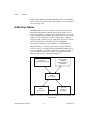
DAQ
PCI/PXI™-6703/6704
User Manual
DC Analog Output Devices
for PCI/PXI/CompactPCI Bus Computers
PCI/PXI-6703/6704 User Manual
March 1999 Edition
Part Number 322110B-01
Worldwide Technical Support and Product Information
www.natinst.com
National Instruments Corporate Headquarters
11500 North Mopac Expressway
Austin, Texas 78759-3504
USA Tel: 512 794 0100
Worldwide Offices
Australia 03 9879 5166, Austria 0662 45 79 90 0, Belgium 02 757 00 20, Brazil 011 284 5011,
Canada (Ontario) 905 785 0085, Canada (Québec) 514 694 8521, China 0755 3904939, Denmark 45 76 26 00,
Finland 09 725 725 11, France 01 48 14 24 24, Germany 089 741 31 30, Hong Kong 2645 3186,
India 91805275406, Israel 03 6120092, Italy 02 413091, Japan 03 5472 2970, Korea 02 596 7456,
Mexico (D.F.) 5 280 7625, Mexico (Monterrey) 8 357 7695, Netherlands 0348 433466, Norway 32 27 73 00,
Singapore 2265886, Spain (Madrid) 91 640 0085, Spain (Barcelona) 93 582 0251, Sweden 08 587 895 00,
Switzerland 056 200 51 51, Taiwan 02 2377 1200, United Kingdom 01635 523545
For further support information, see the Technical Support Resources appendix. To comment on the
documentation, send e-mail to [email protected].
© Copyright 1998, 1999 National Instruments Corporation. All rights reserved.
Important Information
Warranty
The PCI-6703, PXI-6703, PCI-6704, and PXI-6704 are warranted against defects in materials and workmanship for a
period of one year from the date of shipment, as evidenced by receipts or other documentation. National Instruments
will, at its option, repair or replace equipment that proves to be defective during the warranty period. This warranty
includes parts and labor.
The media on which you receive National Instruments software are warranted not to fail to execute programming
instructions, due to defects in materials and workmanship, for a period of 90 days from date of shipment, as evidenced
by receipts or other documentation. National Instruments will, at its option, repair or replace software media that do not
execute programming instructions if National Instruments receives notice of such defects during the warranty period.
National Instruments does not warrant that the operation of the software shall be uninterrupted or error free.
A Return Material Authorization (RMA) number must be obtained from the factory and clearly marked on the outside
of the package before any equipment will be accepted for warranty work. National Instruments will pay the shipping costs
of returning to the owner parts which are covered by warranty.
National Instruments believes that the information in this document is accurate. The document has been carefully
reviewed for technical accuracy. In the event that technical or typographical errors exist, National Instruments reserves
the right to make changes to subsequent editions of this document without prior notice to holders of this edition. The
reader should consult National Instruments if errors are suspected. In no event shall National Instruments be liable for
any damages arising out of or related to this document or the information contained in it.
EXCEPT AS SPECIFIED HEREIN, NATIONAL INSTRUMENTS MAKES NO WARRANTIES, EXPRESS OR IMPLIED, AND
SPECIFICALLY DISCLAIMS ANY WARRANTY OF MERCHANTABILITY OR FITNESS FOR A PARTICULAR PURPOSE. CUSTOMER’S
RIGHT TO RECOVER DAMAGES CAUSED BY FAULT OR NEGLIGENCE ON THE PART OF NATIONAL INSTRUMENTS SHALL BE
LIMITED TO THE AMOUNT THERETOFORE PAID BY THE CUSTOMER. NATIONAL INSTRUMENTS WILL NOT BE LIABLE FOR
DAMAGES RESULTING FROM LOSS OF DATA, PROFITS, USE OF PRODUCTS, OR INCIDENTAL OR CONSEQUENTIAL DAMAGES,
EVEN IF ADVISED OF THE POSSIBILITY THEREOF. This limitation of the liability of National Instruments will apply
regardless of the form of action, whether in contract or tort, including negligence. Any action against National
Instruments must be brought within one year after the cause of action accrues. National Instruments shall not be liable for
any delay in performance due to causes beyond its reasonable control. The warranty provided herein does not cover
damages, defects, malfunctions, or service failures caused by owner’s failure to follow the National Instruments
installation, operation, or maintenance instructions; owner’s modification of the product; owner’s abuse, misuse, or
negligent acts; and power failure or surges, fire, flood, accident, actions of third parties, or other events outside reasonable
control.
Copyright
Under the copyright laws, this publication may not be reproduced or transmitted in any form, electronic or mechanical,
including photocopying, recording, storing in an information retrieval system, or translating, in whole or in part, without
the prior written consent of National Instruments Corporation.
Trademarks
ComponentWorks™, CVI™, LabVIEW™, natinst.com™, NI-DAQ™, PXI™, RTSI™, SCXI™, and VirtualBench™ are
trademarks of National Instruments Corporation.
Product and company names mentioned herein are trademarks or trade names of their respective companies.
WARNING REGARDING MEDICAL AND CLINICAL USE OF NATIONAL INSTRUMENTS PRODUCTS
National Instruments products are not designed with components and testing for a level of reliability suitable for use in
or in connection with surgical implants or as critical components in any life support systems whose failure to perform
can reasonably be expected to cause significant injury to a human. Applications of National Instruments products
involving medical or clinical treatment can create a potential for death or bodily injury caused by product failure, or by
errors on the part of the user or application designer. Because each end-user system is customized and differs from
National Instruments testing platforms and because a user or application designer may use National Instruments products
in combination with other products in a manner not evaluated or contemplated by National Instruments, the user or
application designer is ultimately responsible for verifying and validating the suitability of National Instruments products
whenever National Instruments products are incorporated in a system or application, including, without limitation,
the appropriate design, process and safety level of such system or application.
Conventions
The following conventions are used in this manual:
<>
Angle brackets that contain numbers separated by an ellipsis represent a
range of values associated with a bit or signal name—for example,
DBIO<3..0>.
♦
The ♦ symbol indicates that the following text applies only to a specific
product, a specific operating system, or a specific software version.
This icon denotes a note, which alerts you to important information.
This icon denotes a caution, which advises you of precautions to take to
avoid injury, data loss, or a system crash.
bold
Bold text denotes items that you must select or click on in the software,
such as menu items and dialog box options. Bold text also denotes
parameter names.
italic
Italic text denotes variables, emphasis, a cross reference, or an introduction
to a key concept. This font also denotes text that is a placeholder for a word
or value that you must supply.
monospace
Text in this font denotes text or characters that you should enter from the
keyboard, sections of code, programming examples, and syntax examples.
This font is also used for the proper names of disk drives, paths, directories,
programs, subprograms, subroutines, device names, functions, operations,
variables, filenames and extensions, and code excerpts.
NI-DAQ
NI-DAQ refers to the NI-DAQ driver software.
Abbreviations, acronyms, definitions, metric prefixes, mnemonics, and
symbols are listed in the Glossary.
Contents
Chapter 1
Introduction
About the PCI/PXI-6703/6704 ......................................................................................1-1
What You Need to Get Started ......................................................................................1-2
Unpacking ......................................................................................................................1-2
Software Programming Choices ....................................................................................1-3
National Instruments Application Software ....................................................1-3
NI-DAQ Driver Software ................................................................................1-4
Optional Equipment .......................................................................................................1-5
Custom Cabling ...............................................................................................1-5
Chapter 2
Installation and Configuration
Software Installation ......................................................................................................2-1
Hardware Installation.....................................................................................................2-1
Device Configuration.....................................................................................................2-2
Chapter 3
Signal Connections
I/O Connector Pin Assignments ....................................................................................3-1
Signal Connection Descriptions ......................................................................3-3
Analog Output Signal Connections ...............................................................................3-4
Voltage Output ................................................................................................3-4
Power-up Condition ..........................................................................3-4
Current Output for the 6704 ............................................................................3-5
Power-up Condition ..........................................................................3-6
Digital I/O Signal Connections......................................................................................3-6
Power-up Condition.........................................................................................3-7
Power Connections ........................................................................................................3-7
Chapter 4
Hardware Overview
Bus Interface Circuitry...................................................................................................4-2
I/O Connector ................................................................................................................4-2
Nonvolatile RAM/DAC Control....................................................................................4-2
Digital I/O Control.........................................................................................................4-2
Temperature Sensor .......................................................................................................4-2
© National Instruments Corporation
v
PCI/PXI-6703/6704 User Manual
Contents
Chapter 5
Calibration
Self-Calibration ............................................................................................................. 5-1
External Calibration....................................................................................................... 5-1
Voltage Output Calibration ........................................................................................... 5-3
Offset Adjustment ........................................................................................... 5-3
Gain Adjustment ............................................................................................. 5-3
Current Output Calibration for the 6704 ....................................................................... 5-3
Offset Adjustment ........................................................................................... 5-3
Gain Adjustment ............................................................................................. 5-4
Saving Calibration Values............................................................................................. 5-4
Appendix A
Specifications
Appendix B
Common Questions
Appendix C
Technical Support Resources
Glossary
Index
Figures
Figure 1-1.
The Relationship between the Programming Environment,
NI-DAQ, and Your Hardware................................................................. 1-4
Figure 3-1.
Figure 3-2.
Figure 3-3.
Figure 3-4.
I/O Connector Pin Assignments.............................................................. 3-2
VCH Connection as a Voltage Output.................................................... 3-4
ICH Connection as a Current Output...................................................... 3-5
Example Digital I/O Connections ........................................................... 3-6
Figure 4-1.
PCI/PXI-6703/6704 Block Diagram....................................................... 4-1
Tables
Table 5-1.
Table 5-2.
6703 Calibration Channel Numbers........................................................ 5-2
6704 Calibration Channel Numbers........................................................ 5-2
PCI/PXI-6703/6704 User Manual
vi
www.natinst.com
1
Introduction
This manual describes the mechanical and electrical aspects of the 6703
and 6704 devices and contains information concerning their configuration,
installation, and operation. The 6703 and 6704 devices are designed for
precise DC setpoint applications and provide general-purpose digital I/O.
Unless otherwise noted, text applies to all 6703 and 6704 devices: the
PCI-6703, PXI-6703, PCI-6704 and PXI-6704.
This chapter describes the 6703/6704 devices, lists what you need to get
started, describes software programming choices, optional equipment, and
custom cables, and explains how to unpack your device.
About the PCI/PXI-6703/6704
Thank you for purchasing a National Instruments 6703/6704 device. The
6703/6704 devices are precise DC setpoint devices for PCI and PXI. The
6703 devices have 16 voltage output channels. The 6704 devices have
16 voltage output channels and 16 current output channels for a total of 32
analog output channels. Both 6703 and 6704 devices have eight digital I/O
lines.
You can use the 6703/6704 devices in a wide variety of DC setpoint and
digital I/O applications. With the 6703/6704 devices, your PC system can
serve as a digital I/O system controller for laboratory testing, production
testing, and industrial process monitoring and control. These devices can
do the following:
•
Generate experimental stimuli
•
Generate analog functions
•
Connect to a variety of signal types, including:
© National Instruments Corporation
–
Electromechanical relays
–
LEDs
–
Optically isolated, solid-state relays and I/O module mounting
racks
–
Voltage and current excitation for precision transducers
–
Current excitation for precision transducers (6704 only)
1-1
PCI/PXI-6703/6704 User Manual
Chapter 1
Introduction
Detailed specifications for the 6703/6704 devices are in Appendix A,
Specifications.
What You Need to Get Started
To set up and use your 6703/6704 device, you will need the following:
❑ One of the following devices:
•
PCI-6703
•
PXI-6703
•
PCI-6704
•
PXI-6704
❑ PCI/PXI-6703/6704 User Manual
❑ One of the following software packages and documentation:
•
ComponentWorks
•
LabVIEW for Windows
•
LabWindows/CVI for Windows
•
Measure
•
NI-DAQ for PC compatibles
•
VirtualBench
❑ PC with a free PCI slot or PXI chassis with a free slot
❑ 68-pin cable (type SH68-68-D1)
❑ 68-pin terminal block (type CB-68)
Unpacking
Your 6703/6704 device is shipped in an antistatic package to prevent
electrostatic damage to the device. Electrostatic discharge can damage
several components on the device. To avoid such damage in handling the
device, take the following precautions:
PCI/PXI-6703/6704 User Manual
•
Ground yourself via a grounding strap or by holding a grounded
object.
•
Touch the antistatic package to a metal part of your PC chassis
before removing the device from the package.
1-2
www.natinst.com
Chapter 1
Introduction
•
Remove the device from the package and inspect the device for
loose components or any other sign of damage. Notify National
Instruments if the device appears damaged in any way. Do not
install a damaged device into your computer.
•
Never touch the exposed pins of connectors.
Software Programming Choices
There are several options to choose from when programming your National
Instruments DAQ hardware. You can use LabVIEW, LabWindows/CVI,
ComponentWorks, VirtualBench, or other application development
environments in conjunction with NI-DAQ.
National Instruments Application Software
ComponentWorks contains tools for data acquisition and instrument
control built on NI-DAQ driver software. ComponentWorks provides a
higher-level programming interface for building virtual instruments
through standard OLE controls and DLLs. With ComponentWorks, you
can use all of the configuration tools, resource management utilities, and
interactive control utilities included with NI-DAQ.
LabVIEW features interactive graphics, a state-of-the-art user interface,
and a powerful graphical programming language. The LabVIEW Data
Acquisition VI Library, a series of VIs for using LabVIEW with National
Instruments DAQ hardware, is included with LabVIEW. The LabVIEW
Data Acquisition VI Library is functionally equivalent to the NI-DAQ
software.
LabWindows/CVI features interactive graphics, a state-of-the-art user
interface, and uses the ANSI standard C programming language. The
LabWindows/CVI Data Acquisition Library, a series of functions for using
LabWindows/CVI with National Instruments DAQ hardware, is included
with the NI-DAQ software kit. The LabWindows/CVI Data Acquisition
Library is functionally equivalent to the NI-DAQ software.
VirtualBench features VIs that combine DAQ products, software, and your
computer to create a standalone instrument with the added benefit of the
processing, display, and storage capabilities of your computer.
VirtualBench instruments load and save waveform data to disk in the same
forms that can be used in popular spreadsheet programs and word
processors.
© National Instruments Corporation
1-3
PCI/PXI-6703/6704 User Manual
Chapter 1
Introduction
Using ComponentWorks, LabVIEW, LabWindows/CVI, or VirtualBench
software will greatly reduce the development time for your data acquisition
and control application.
NI-DAQ Driver Software
The NI-DAQ driver software is included at no charge with all National
Instruments DAQ hardware. NI-DAQ is not packaged with accessory
products. NI-DAQ has an extensive library of functions that you can call
from your application programming environment. These functions include
routines for analog input (A/D conversion), buffered data acquisition
(high-speed A/D conversion), analog output (D/A conversion), waveform
generation, digital I/O, counter/timer operations, SCXI, RTSI,
self-calibration, messaging, and acquiring data to extended memory.
NI-DAQ maintains a consistent software interface among its different
versions so that you can change platforms with minimal modifications to
your code. Whether you are using conventional programing languages or
National Instruments application software, your application uses the
NI-DAQ driver software, as illustrated in Figure 1-1.
Conventional
Programming Environment
ComponentWorks,
LabVIEW,
LabWindows/CVI, or
VirtualBench
NI-DAQ
Driver Software
DAQ or
SCXI Hardware
Personal
Computer or
Workstation
Figure 1-1. The Relationship between the Programming Environment, NI-DAQ, and
Your Hardware
PCI/PXI-6703/6704 User Manual
1-4
www.natinst.com
Chapter 1
Introduction
Optional Equipment
National Instruments offers a variety of products to use with your
6703/6704 device, including cables, connector blocks, and other
accessories, as follows:
•
Cables and cable assemblies, shielded and ribbon
•
Connector blocks, shielded and unshielded screw terminals
For more information about these products, refer to the National
Instruments catalogue or website or call the office nearest you.
Custom Cabling
National Instruments offers cables and accessories for you to prototype
your application or to use if you frequently change module
interconnections.
If you want to develop your own cable, mating connectors and a backshell
kit for making custom 68-pin cables are available from National
Instruments (part number 776832-01).
Refer to your National Instruments catalogue for specific information.
© National Instruments Corporation
1-5
PCI/PXI-6703/6704 User Manual
2
Installation and Configuration
This chapter explains how to install and configure your 6703/6704 device.
Software Installation
Install your software before you install your 6703/6704 device. Refer to the
appropriate release notes indicated below for specific instructions on the
software installation sequence.
1.
Install your application software—If you are using LabVIEW,
LabWindows/CVI, or other National Instruments application software
packages, refer to the appropriate release notes.
2.
Install the NI-DAQ driver software—Refer to your NI-DAQ release
notes and follow the instructions given there for your operating system
and application software package.
You can now install your hardware.
Hardware Installation
You can install your 6703/6704 device in any available expansion slot in
your computer. However, to achieve best noise performance, leave as much
room as possible between your 6703/6704 device and other boards and
hardware. The following are general installation instructions, but consult
your computer user manual or technical reference manual for specific
instructions and warnings.
♦
PCI-6703/6704
1.
Turn off and unplug your computer.
2.
Remove the top cover or access port to the I/O channel.
3.
Remove the expansion slot cover on the back panel of the computer.
4.
Touch any metal part of your computer chassis to discharge any static
electricity that might be on your clothes or body.
5.
Insert the PCI-6703/6704 into a 5 V PCI slot. Gently rock the device
to ease it into place. Do not force the device into place.
© National Instruments Corporation
2-1
PCI/PXI-6703/6704 User Manual
Chapter 2
Installation and Configuration
6.
Screw the mounting bracket of the PCI-6703/6704 device to the back
panel rail of the computer.
7.
Visually verify the installation.
8.
Replace the cover.
9.
Plug in and turn on your computer.
Your PCI-6703/6704 is installed. You are now ready to configure your
hardware and software.
♦
PXI-6703/6704
1.
Turn off and unplug your PXI controller.
2.
Choose an unused PXI slot in your system.
3.
Remove the filler panel for the slot you have chosen.
4.
Touch any metal part of your computer chassis to discharge any static
electricity that might be on your clothes or body.
5.
Insert the PXI-6703/6704 into a PXI chassis slot. Use the
injector/ejector handle to fully insert the device into the chassis.
6.
Screw the front panel of the PXI-6703/6704 to the front panel
mounting rail of the system.
7.
Visually verify the installation.
8.
Plug in and turn on your computer.
Your PXI-6703/6704 is installed. You are now ready to configure your
hardware and software.
Device Configuration
Due to the National Instruments standard architecture for data acquisition
and the PCI and PXI bus specifications, all 6703 and 6704 devices are
completely software-configurable. Refer to your software documentation
for configuration instructions.
The PCI-6703/6704 are fully compatible with the industry-standard PCI
Local Bus Specification Revision 2.0, and the PXI-6703/6704 are fully
compatible with the PXI Specification Revision 1.0. These specifications
allow the PCI and PXI systems to automatically perform all bus-related
configurations and require no user interaction. Bus-related configuration
includes setting the device base memory address and interrupt channel.
PCI/PXI-6703/6704 User Manual
2-2
www.natinst.com
3
Signal Connections
This chapter provides connection instructions for the signals on your
6703/6704 device I/O connector.
Connections that exceed any of the maximum ratings of input or output signals
on the 6703/6704 device can damage the device and the computer. Maximum input ratings
for each signal are given in this chapter under the discussion of that signal. National
Instruments is NOT liable for any damages resulting from any incorrect signal connections.
Warning
I/O Connector Pin Assignments
Figure 3-1 shows the I/O connector pin assignments for the
6703/6704 devices.
© National Instruments Corporation
3-1
PCI/PXI-6703/6704 User Manual
Chapter 3
Signal Connections
+5V
DIO0
DIO1
DIO2
DIO3
DIO4
DIO5
DIO6
DIO7
ICH31*
AGND15/AGND31
VCH14
ICH29*
AGND13/AGND29
VCH12
ICH27*
VCH11
AGND10/AGND26
AGND
AGND9/AGND25
ICH24*
VCH8
ICH23*
AGND7/AGND23
VCH6
ICH21*
1
2
3
4
5
6
7
8
9
10
11
12
13
14
15
16
17
18
19
20
21
22
23
24
25
26
35
36
37
38
39
40
41
42
43
44
45
46
47
48
49
50
51
52
53
54
55
56
57
58
59
DGND
60
VCH5
DGND
DGND
RFU
DGND
RFU
DGND
DGND
AGND
VCH15
ICH30*
AGND14/AGND30
VCH13
ICH28*
AGND12/AGND28
AGND11/AGND27
ICH26*
VCH10
ICH25*
VCH9
AGND8/AGND24
AGND
VCH7
ICH22*
AGND6/AGND22
AGND5/AGND21
27 61
ICH20*
VCH4
ICH19*
AGND4/AGND20
AGND3/AGND19
28 62
29 63
30 64
VCH2
31 65
AGND2/AGND18
ICH17*
32 66
VCH1
AGND1/AGND17
33 67
34 68
ICH16*
VCH0
VCH3
ICH18*
AGND0/AGND16
* No connects on the PCI/PXI 6703
Figure 3-1. I/O Connector Pin Assignments
PCI/PXI-6703/6704 User Manual
3-2
www.natinst.com
Chapter 3
Signal Connections
Signal Connection Descriptions
Pin
<2..9>
<35..37>, 39, 41, 42
Signal Name
Description
DIO<0..7>
Digital Input/Output lines—Line 7 is the
MSB and Line 0 is the LSB.
DGND
Digital Ground—These pins are connected
to the 6703/6704 device digital ground
plane. All 6703/6704 device ground planes
connect to the computer system’s ground
signal.
1
+5V
+5 V—This pin is connected to the
computer system’s +5 VDC supply through
a self-resetting circuit breaker.
38, 40
RFU
Reserved for future use.
34, 66, 31, 63, 28, 60, 25,
57, 22, 54, 52, 17, 15, 47,
12, 44
VCH<0..15>
Voltage output channels.
67, 32, 64, 29, 61, 26, 58,
23, 21, 53, 51, 16, 48, 13,
45, 10
ICH<16..31>
Current output channels on the 6704.
68, 33, 65, 30, 62, 27, 59,
24, 55, 20, 18, 50, 49, 14,
46, 11
AGND<0/16..15/31>
19, 43, 56
© National Instruments Corporation
No connects on the 6703.
AGND
Analog Grounds—Each ground pin is
shared between one voltage and one current
channel. These pins are connected to the
6703/6704 device analog ground plane. All
6703/6704 device ground planes connect to
the computer system’s ground signal.
Additional pins connected to analog
ground.
3-3
PCI/PXI-6703/6704 User Manual
Chapter 3
Signal Connections
Analog Output Signal Connections
This section describes how to make connections for voltage and current
outputs. The 6704 has both voltage and current outputs, however, the 6703
has voltage outputs only. A 68-pin cable such as the SH68-68-D1 cable is
required. Figure 3-2 shows how to connect the voltage channel (VCH)
outputs.
VCH
±10.1 V
Load
AGND
A
PCI/PXI-6703/6704
Floating Load
Figure 3-2. VCH Connection as a Voltage Output
Voltage Output
You can connect a floating load to your 6703/6704 device at the voltage
output channel.
Because 6703/6704 devices are not electrically isolated from high voltages, a
load with high common-mode voltages can damage the devices. National Instruments is
NOT liable for any damages resulting from any such signal connections.
Warning
Your 6703/6704 device has a bipolar voltage range of –10.1 to +10.1 V.
Maximum load current is ±10 mA for 16-bit linearity.
Power-up Condition
All voltage outputs are at their user-defined values to full accuracy within
1 s of power-up board reset. Before this time, the voltage outputs can float
to unspecified values. Take this behavior into account when connecting
external devices to the 6703/6704.
PCI/PXI-6703/6704 User Manual
3-4
www.natinst.com
Chapter 3
Signal Connections
Current Output for the 6704
You can connect a floating or grounded load to your 6704 device at the
current output channel. You do not need an external floating power supply
to complete the controlled current loop. You can control the current loop
from 0.1 to 20.2 mA. The compliance for the current loop is 0 V to
10 VDC.
Because 6704 devices are not electrically isolated from high voltages, a load
with high common-mode voltages can damage the 6704 devices. National Instruments is
NOT liable for any damages resulting from any such signal connections.
Warning
Figure 3-3 shows how to connect a current channel (ICH) as a current
output.
ICH
Load
0.1 to 20.2 mA
AGND
PCI/PXI-6704
Figure 3-3. ICH Connection as a Current Output
Because each current channel shares a ground line with a voltage channel,
you should try to minimize the effect of the return current from your current
channel on the voltage that you are outputting on your voltage channel. For
example, if you output 20 mA on a current channel and return that current
to the 6704 device along the shared ground line in a cable with an
impedance of 0.1 Ω, you will see a 2 mV drop in the voltage output by the
© National Instruments Corporation
3-5
PCI/PXI-6703/6704 User Manual
Chapter 3
Signal Connections
voltage channel sharing the ground line. You can approach this problem in
the following ways:
–
Use a shorter cable to minimize the impedance of the shared
ground line.
–
Use separate wiring for VCH and ICH ground return to minimize
common ground impedance.
–
Use different pairs of voltage and current channels to keep your
sensitive voltage outputs separate from your higher output current
channels.
Power-up Condition
All current outputs are within ± 1.1 mA maximum of their user-defined
values within 0.5 s of power-up board reset. The current outputs will settle
to their user-defined values to full accuracy within 7 s of power-up board
reset. Take this behavior into account when connecting external devices to
the 6704.
Digital I/O Signal Connections
Figure 3-4 illustrates example signal connections for three typical digital
I/O applications.
+5 V
LED
Line 0
R
Line 1
DIO
Line<0..7>
TTL Signal
Line 2
+5 V
Switch
DGND
I/O Connector
PCI/PXI-6703/6704
Figure 3-4. Example Digital I/O Connections
PCI/PXI-6703/6704 User Manual
3-6
www.natinst.com
Chapter 3
Signal Connections
In Figure 3-4, line 0 is configured for digital output; lines 1 and 2 are
configured for digital input.
Digital input applications include receiving TTL signals and sensing
external device states such as the switch in Figure 3-4. Digital output
applications include sending TTL signals and driving external devices such
as the LED shown in Figure 3-4.
The 6703/6704 devices allow line-by-line direction control of digital I/O
connections.
Note
Refer to Appendix A, Specifications, for a list of the digital I/O signal
ratings.
Power-up Condition
At power up, all of the DIO lines on the 6703/6704 devices are configured
as input lines.
Power Connections
Pin 1 on the I/O connector is connected to the +5 V supply from the PCI or
PXI bus power supply. This pin is referenced to DGND and can supply
power to external circuitry. The +5 V supply has a total of 0.75 A available.
The +5 V power supply has a self-resetting protection circuit breaker in
series. If the circuit breaker protection is activated, simply remove the
circuit causing the heavy current load and the circuit breaker will reset
itself. For more information on these output pins, see the Digital I/O and
Power Requirement sections in Appendix A, Specifications.
Power rating
0.75 A at +5 V ±10%, +4.55 to
+5.25 VDC at 0.75 A
Under no circumstances should you connect these +5 V power pins directly to
ground or to any other voltage source on your 6703/6704 device or any other device. Doing
so can damage your device and your computer system. National Instruments is NOT liable
for damage resulting from such a connection.
Warning
© National Instruments Corporation
3-7
PCI/PXI-6703/6704 User Manual
4
Hardware Overview
This chapter contains a functional overview of the 6703/6704 devices and
explains the operation of each functional unit making up the devices.
The block diagram in Figure 4-1 illustrates the key functional components
of the 6703/6704 devices.
Control
PCI/PXI Bus
Data
Bus
Interface
Logic
Control
Lines
nvRAM/
DAC
Control
16-Bit
DAC
DAC
Out
RAM Data
RAM
Addr/Ctrl
Main
Voltage
Circuit
16
Voltage
Output
Circuit X 16
Main
Current
Circuit*
16
Current
Output
Circuit X 16*
I/O Connector
Address
nvSRAM
Digital
I/O
DIO Lines <7..0>
Serial
Number
EEPROM
Temperature
Sensor
+5 V
0.75 A
Self-Resetting Circuit Breaker
*No current circuits present on PCI/PXI-6703
Figure 4-1. PCI/PXI-6703/6704 Block Diagram
© National Instruments Corporation
4-1
PCI/PXI-6703/6704 User Manual
Chapter 4
Hardware Overview
Bus Interface Circuitry
The bus interface circuitry monitors the PCI or PXI bus. If the bus address
matches the 6703/6704 device’s address, the board is enabled and the
corresponding register on the 6703/6704 is accessed.
I/O Connector
All user I/O is transmitted through a 68-pin connector. Refer to the Custom
Cabling section in Chapter 1, Introduction, and to Chapter 3, Signal
Connections, for additional information.
Nonvolatile RAM/DAC Control
The 6703/6704 devices have one 16-bit DAC that is time-division
multiplexed to create all the output channels. Each channel has a
track-and-hold circuit to maintain the channel value between DAC updates.
On the 6703, the DAC is multiplexed to create 16 voltage outputs and two
calibration channels. On the 6704, the DAC is multiplexed to create
16 voltage outputs, 16 current outputs, and four calibration channels.
Data is stored in a nonvolatile RAM (nvRAM). The nvRAM/DAC control
reads the DAC channel data stored in the nvRAM and updates the DAC
periodically. The nvRAM/DAC control also controls the analog
demultiplexing circuits to route the DAC output to the correct analog output
channel. You can choose to save nvRAM data so that the current output
values will become the power-on states.
Digital I/O Control
The 6703/6704 devices have eight digital I/O lines configured as one 8-bit
port. You can configure each line independently as an input or output. The
DIO lines have 16 mA of sink capability and 16 mA of source capability.
All digital lines are TTL compatible. At power up, all digital lines are
configured as inputs.
Temperature Sensor
The onboard temperature sensor measures the air temperature flowing over
the board. This sensor is positioned near the onboard precision voltage
reference, which can be affected by extreme temperatures. This sensor has
a serial digital interface.
PCI/PXI-6703/6704 User Manual
4-2
www.natinst.com
5
Calibration
This chapter discusses the calibration procedures for your 6703/6704
device. Calibration is the process of minimizing output errors by making
small circuit adjustments. There are two calibration channels used to make
adjustments to the voltage channels on the 6703/6704. On the 6704, there
are two additional channels used to make adjustments to the current
channels.
Self-Calibration
The 6703/6704 devices perform continuous self-calibration. In addition to
the accessible analog output channels, there are internal calibration
channels that get scanned and refreshed along with all the output channels.
There are two of these calibration channels for the voltage outputs: the
voltage offset channel and the voltage gain channel.
There are also two calibration channels for the current outputs on the 6704:
the current offset channel and the current gain channel. The outputs of these
calibration channels are continuously compared to onboard references, and
the 16-bit DAC offset and gain are adjusted to minimize the errors in the
calibration channels. Since 6703/6704 devices have excellent
channel-to-channel matching of offset and gain errors, minimizing the
errors in the calibration channels also minimizes the errors for all the
voltage and current outputs.
External Calibration
Because of the nature of the 6703/6704 device calibration circuitry, the
only calibration adjustment you must make is to adjust the values of the
calibration channels to account for time- or temperature-related drift of the
onboard reference. These calibration values are loaded into nvRAM at
factory calibration, and you should not need to adjust them for at least one
year after the date of factory calibration, unless you are operating your
device at an extreme temperature.
To perform calibration, you need a voltage and current measuring device
that is much more accurate than your 6703/6704 device. A DMM with an
© National Instruments Corporation
5-1
PCI/PXI-6703/6704 User Manual
Chapter 5
Calibration
accuracy of at least 10 ppm will generally suffice, but be sure to check its
specifications. Also, be sure that no other devices are connected to your
6703/6704 when you calibrate it to ensure that no ground loops can corrupt
the calibration.
Your 6703/6704 device contains a calibration enable bit in a control register
to prevent you from accidentally writing to the calibration channels. Before
you can calibrate the board, you must set this bit. If you are using NI-DAQ,
calibration is enabled by calling the NI-DAQ function
Set_DAQ_Device_Info (deviceNumber, infoType, infoValue) with
infoType equal to ND_CALIBRATION_ENABLE and infoValue equal to
ND_YES. You may then write to the calibration channels by calling
AO_VWrite (deviceNumber, chan, voltage) where chan is the calibration
channel number, and voltage is the channel value to be written.
Table 5-1 lists the channel numbers of the calibration channels for the 6703.
Table 5-1. 6703 Calibration Channel Numbers
Calibration Channel
Channel Number
Voltage offset
Channel 16
Voltage gain
Channel 17
Table 5-2 lists the channel numbers of the calibration channels for the 6704.
Table 5-2. 6704 Calibration Channel Numbers
Calibration Channel
PCI/PXI-6703/6704 User Manual
Channel Number
Voltage offset
Channel 32
Voltage gain
Channel 34
Current offset
Channel 33
Current gain
Channel 35
5-2
www.natinst.com
Chapter 5
Calibration
Voltage Output Calibration
There are two adjustments to make for the voltage outputs: offset and gain.
You should perform offset adjustment first. It is a good idea to calibrate
twice, because a large change in the voltage gain channel value could
impact the accuracy of the offset calibration.
Offset Adjustment
To calibrate the offset, set one of the voltage output channels to 0 V and
measure it with a precise voltmeter. Then, change the voltage offset
channel value until the output is zero. The voltage you write to the voltage
offset channel will be close to zero, and increasing it will lower the voltage
you measure.
Gain Adjustment
To calibrate the gain, set the voltage output channel to a voltage near
full-scale, such as +10 V. Then, change the voltage gain channel value until
the output that you measure is as close as possible to the voltage that you
wrote to the output channel. The voltage you write to the voltage gain
channel will be close to +10 V, and increasing it will lower the magnitude
of the voltage you measure.
You can also calibrate using several output channels, instead of just one, by
averaging channels together. Do this by writing the values to all the
channels you wish to average and using a resistive averaging circuit to
average the outputs. This will reduce the sensitivity of the calibration
process to interchannel mismatch—the slight differences in the output
characteristics of the channels—by averaging out these differences.
Current Output Calibration for the 6704
There are two adjustments to make for the current outputs: offset and gain.
You should perform offset adjustment first. It is a good idea to calibrate
twice, because a large change in the current gain channel value could
impact the accuracy of the offset calibration.
Offset Adjustment
To calibrate the offset, set one of the current output channels to 100 µA and
measure it with a precise ammeter. Then, change the current offset channel
value until the output is as close as possible to 100 µA. The current you
© National Instruments Corporation
5-3
PCI/PXI-6703/6704 User Manual
Chapter 5
Calibration
write to the current offset channel will be close to 10 µA, and increasing it
will lower the current you measure.
Gain Adjustment
To calibrate the gain, set the current output channel to a current near
full-scale, such as 20 mA. Then, change the current gain channel value
until the output that you measure is as close as possible to the current that
you wrote to the output channel. The current you write to the current gain
channel will be close to 19.608 mA, and increasing it will lower the current
you measure.
You can also calibrate using several output channels instead of just one by
adding channels together. Do this by writing the values to all the channels
you wish to add and summing the outputs by connecting them together.
This will reduce the sensitivity of the calibration process to interchannel
mismatch—the slight differences in the output characteristics of the
channels by averaging out these differences.
Saving Calibration Values
When you have finished calibration, you will want to write your calibration
values into nvRAM. This will ensure that your new calibration values are
permanently saved and automatically loaded when the card is powered-on.
Calibration values are saved and restored through the AO_Calibrate
(deviceNumber, operation, EEPROMloc) function call in NI-DAQ. To
save your calibration values, make the following call: AO_Calibrate
(deviceNumber, 2, 1), where deviceNumber refers to the device number
assigned by the NI-DAQ Configuration Utility. If you need to restore the
factory calibration values, load them by calling AO_Calibrate
(deviceNumber, 1, 5). For more information, consult the NI-DAQ
Function Reference Manual.
PCI/PXI-6703/6704 User Manual
5-4
www.natinst.com
A
Specifications
This appendix lists specifications for 6703/6704 devices. These
specifications are valid for an ambient temperature of 0° to 55 °C, unless
otherwise stated.
Analog Output
Number of voltage channels .................. 16
Number of current channels
for the 6704 ............................................ 16
Resolution .............................................. 16-bit
Recommended warm-up time ................ 15 minutes
Transfer Characteristics
INL ......................................................... ±1 LSB max
DNL ....................................................... ±1 LSB max
Monotonicity.......................................... 16 bits, guaranteed
Voltage Output
Range ..................................................... ±10.1 V
Output coupling...................................... DC
Output impedance .................................. 0.1 Ω max
Current drive .......................................... ±10 mA max
Load capacitance.................................... 10,000 pF max
Protection ............................................... Short-circuit to ground
© National Instruments Corporation
A-1
PCI/PXI-6703/6704 User Manual
Appendix A
Specifications
Absolute accuracy...................................±1 mV max
Noise .......................................................100 µV rms, DC to 1 MHz
Power-up state ........................................Independent, user-defined values
Current Output, 6704 Only
Range ......................................................0.1 to 20.2 mA
Type ........................................................Source, does not require external
excitation source
Output impedance...................................1 GΩ min
Output compliance..................................0 to 10 V
Absolute accuracy...................................±2 µA max
Noise .......................................................1 µA rms, DC to 1 MHz
Protection................................................Short-circuit and open circuit
Power-up state ........................................Independent, user-defined values
Dynamic Characteristics
Settling time (including channel latency)
Accuracy
Time
±0.1%
1.8 ms typ, 5.6 ms max
±0.01%
3.6 ms typ, 11.2 ms max
±0.001%
14.4 ms typ, 48.8 ms max
Stability
Offset temperature coefficient
Voltage ............................................5 µV/ ºC
Current (6704 only) .........................10 nA/ ºC
PCI/PXI-6703/6704 User Manual
A-2
www.natinst.com
Appendix A
Specifications
Gain temperature coefficient
Voltage............................................ 1 ppm/ ºC
Current (6704 only) ........................ 2 ppm/ ºC
Digital I/O
Number of channels ............................... 8 I/O
Compatibility ......................................... TTL
Power-on state........................................ Input (high impedance)
Digital logic levels
Level
Min
Max
Input low voltage
—
0.8 V
Input high voltage
2.0 V
—
Output low voltage
—
0.45 V, IOL = 16 mA
Output high voltage
2.4 V, IOH = 16 mA
—
Input leakage current
—
10 µA
Bus Interface
Type ....................................................... Slave
Power Requirement
+5 V
6703 ................................................ 700 mA
6704 ................................................ 1 A
+12 V...................................................... 70 mA
–12 V...................................................... 70 mA
© National Instruments Corporation
A-3
PCI/PXI-6703/6704 User Manual
Appendix A
Specifications
These power usage figures do not include the power used by external devices that
are connected to the fused supply present on the I/O connector. They assume that all
voltage and current outputs are fully loaded.
Note
Physical
Dimensions (not including connectors)
PCI-6703/6704 ................................9.9 by 17.5 cm (3.9 by 6.9 in.)
PXI-6703/6704 ................................10 by 16 cm (3.9 by 6.3 in.)
I/O connector ..........................................68-pin male
Environment
Operating
Temperature............................................0° to 55 °C ambient
Relative humidity ...................................5% to 90% noncondensing
Storage
Temperature............................................–20° to 70 °C ambient
Relative humidity ...................................5% to 90% noncondensing
PCI/PXI-6703/6704 User Manual
A-4
www.natinst.com
B
Common Questions
This appendix contains commonly asked questions and their answers
relating to usage and special features of your 6703/6704 device.
General Information
What if I short-circuit the power supply on the 6703/6704 connector?
Pin 1 of the I/O connector is connected to the +5 V supply from the PCI or
PXI bus power supply. This pin is referenced to GND and can be used to
power external circuitry. The +5 V supply has a total of 0.75 A available.
This power supply has a self-resetting protection circuit breaker in series.
If the circuit breaker protection is activated, simply remove the circuit
causing the heavy current load and the circuit breaker will reset itself. For
more information on this output pin, see the Power Requirement section in
Appendix A, Specifications.
Installation and Configuration
Which National Instruments document should I read first to get
started using DAQ software?
The release notes document for your application or driver software is
always the best starting place.
What version of NI-DAQ must I have to program my 6703 device?
You must have NI-DAQ for PC compatibles version 6.6 or higher for your
6703 device.
What version of NI-DAQ must I have to program my 6704 device?
You must have NI-DAQ for PC compatibles version 6.5 or higher for your
6704 device.
© National Instruments Corporation
B-1
PCI/PXI-6703/6704 User Manual
Appendix B
Common Questions
What is the best way to test my device without having to program it?
The Measurement and Automation Explorer has a Test panel with some
excellent tools for doing simple functional tests of the device, such as
testing the digital I/O lines. Also, the Test Configuration button will verify
that the logical address for the device is current.
Timing and Digital I/O
What are the power-on states of the DIO lines on the I/O connector?
At system power-on and reset, all lines are configured as inputs. Refer to
the Digital I/O Control section in Chapter 4, Hardware Overview, for more
information.
Analog Output
What are the power-on states of the voltage and current outputs?
At system power-on and reset, all analog outputs are at the values you last
saved.
How fast do the 6703 devices scan channels?
The 6703 devices have one 16-bit DAC that is time-division multiplexed to
create 16 voltage output and two calibration channels. The channels are
scanned at a rate of 50 µs per channel, thus a channel can change value a
maximum of 0.9 ms after it has been updated by software.
How fast do the 6704 devices scan channels?
The 6704 devices have one 16-bit DAC that is time-division multiplexed to
create 16 voltage output, 16 current output, and four calibration channels.
The channels are scanned at a rate of 50 µs per channel, thus a channel can
change value a maximum of 1.8 ms after it has been updated by software.
PCI/PXI-6703/6704 User Manual
B-2
www.natinst.com
C
Technical Support Resources
National Instruments offers technical support through electronic, fax, and
telephone systems. The electronic services include our Web site, an FTP
site, and a fax-on-demand system. If you have a hardware or software
problem, please first try the electronic support systems. If the information
available on these systems does not answer your questions, contact one of
our technical support centers, which are staffed by applications engineers,
for support by telephone and fax. To comment on the documentation
supplied with our products, send e-mail to [email protected].
Web Site
The InstrumentationWeb address is www.natinst.com.
From this Web site you can connect to our Web sites around the
world (www.natinst.com/niglobal/) and access technical
support (www.natinst.com/support/).
FTP Site
To access our FTP site, log in to our Internet host, ftp.natinst.com,
as anonymous and use your e-mail address, such as
[email protected], as your password. The support files and
documents are located in the \support directories.
Fax-on-Demand Support
Fax-on-Demand is a 24-hour information retrieval system containing a
library of documents in English on a wide range of technical information.
You can access Fax-on-Demand from a touch-tone telephone at
512 418 1111.
E-Mail Support
You can submit technical support questions to the applications engineering
team through e-mail at [email protected]. Remember to include
your name, address, and phone number so we can contact you with
solutions and suggestions.
© National Instruments Corporation
C-1
PCI/PXI-6703/6704 User Manual
Telephone and Fax Support
For telephone support in the United States, dial 512 795 8248. For
telephone support outside the United States, contact your local branch
office:
Australia 03 9879 5166, Austria 0662 45 79 90 0, Belgium 02 757 00 20,
Brazil 011 284 5011, Canada (Ontario) 905 785 0085,
Canada (Québec) 514 694 8521, China 0755 3904939,
Denmark 45 76 26 00, Finland 09 725 725 11, France 01 48 14 24 24,
Germany 089 741 31 30, Hong Kong 2645 3186, India 91805275406,
Israel 03 6120092, Italy 02 413091, Japan 03 5472 2970,
Korea 02 596 7456, Mexico (D.F.) 5 280 7625,
Mexico (Monterrey) 8 357 7695, Netherlands 0348 433466,
Norway 32 27 73 00, Singapore 2265886, Spain (Madrid) 91 640 0085,
Spain (Barcelona) 93 582 0251, Sweden 08 587 895 00,
Switzerland 056 200 51 51, Taiwan 02 2377 1200,
United Kingdom 01635 523545
PCI/PXI-6703/6704 User Manual
C-2
www.natinst.com
Glossary
Prefix
Meaning
Value
n-
nano-
10–9
µ-
micro-
10–6
m-
milli-
10–3
k-
kilo-
103
M-
mega-
106
G-
giga-
109
Numbers/Symbols
°
degrees
–
negative of, or minus
Ω
ohms
/
per
%
percent
±
plus or minus
+
positive of, or plus
A
A
amperes
A/D
analog-to-digital
ANSI
American National Standards Institute
© National Instruments Corporation
G-1
PCI/PXI-6703/6704 User Manual
Glossary
B
bit
one binary digit, either 0 or 1
bus
the group of conductors that interconnect individual circuitry in a computer.
Typically, a bus is the expansion vehicle to which I/O or other devices are
connected.
C
C
Celsius
channel
pin or wire lead to which you apply or from which you read the analog or
digital signal. Analog signals can be single-ended or differential. For digital
signals, you group channels to form ports. Ports usually consist of either
four or eight digital channels.
D
D/A
digital-to-analog
DAC
D/A converter
DAQ
data acquisition—(1) collecting and measuring electrical signals from
sensors, transducers, and test probes or fixtures and inputting them to a
computer for processing; (2) collecting and measuring the same kinds of
electrical signals with A/D and/or DIO boards plugged into a computer, and
possibly generating control signals with D/A and/or DIO boards in the
same computer
DC
direct current
device
(1) a plug-in data acquisition board, card, or pad that can contain multiple
channels and conversion devices. Plug-in boards, PCMCIA cards, and
devices such as the DAQPad-1200, which connects to your computer
parallel port, are all examples of DAQ devices.
DIO
digital input/output
PCI/PXI-6703/6704 User Manual
G-2
© National Instruments Corporation
Glossary
DLL
Dynamic Link Library—A software module in Microsoft Windows
containing executable code and data that can be called or used by Windows
applications or by other DLLs. Functions and data in a DLL are loaded and
linked at run time when they are referenced by a Windows application or
other DLLs.
drivers/driver software
software that controls a specific hardware device such as a DAQ board
E
EEPROM
Electrically Erasable Programmable Read-Only Memory (ROM) that can
be erased (usually by ultraviolet light exposure) and reprogrammed
F
function
a set of software instructions executed by a single line of code that may
have input and/or output parameters and returns a value when executed
G
GND
ground signal or bit
H
hardware
the physical components of a computer system, such as the circuit boards,
plug-in boards, chassis, enclosures, peripherals, cables, and so on
hex
hexadecimal
Hz
hertz—the number of scans read or updates written per second
I
IC
integrated circuit
in.
inches
INL
Integral Nonlinearity—a measure in LSB of the worst-case deviation from
the ideal A/D or D/A transfer characteristic of the analog I/O circuitry
© National Instruments Corporation
G-3
PCI/PXI-6703/6704 User Manual
Glossary
interrupt
a computer signal indicating that the CPU should suspend its current task
to service a designated activity
interrupt level
the relative priority at which a device can interrupt
I/O
input/output—the transfer of data to/from a computer system involving
communications channels, operator interface devices, and/or data
acquisition and control interfaces
IOH
current, output high
IOL
current, output low
K
KB
kilobytes—1,024 bytes when referring to memory
L
LED
light-emitting diode
LSB
least significant bit
M
m
meters
max
maximum
min
minimum
MSB
most significant bit
N
NC
not connected
NI-DAQ
National Instruments driver software for DAQ hardware
PCI/PXI-6703/6704 User Manual
G-4
© National Instruments Corporation
Glossary
noise
an undesirable electrical signal—Noise comes from external sources such
as the AC power line, motors, generators, transformers, fluorescent lights,
soldering irons, CRT displays, computers, electrical storms, welders, radio
transmitters, and internal sources such as semiconductors, resistors, and
capacitors. Noise corrupts signals you are trying to send or receive.
nvRAM
nonvolatile RAM
O
operating system
base-level software that controls a computer, runs programs, interacts with
users, and communicates with installed hardware or peripheral devices
P
PC
personal computer
port
(1) a communications connection on a computer or a remote controller (2)
a digital port, consisting of four or eight lines of digital input and/or output
ppm
parts per million
R
RAM
random access memory
resolution
the smallest signal increment that can be detected by a measurement
system. Resolution can be expressed in bits, in proportions, or in percent of
full scale. For example, a system has 12-bit resolution, one part in 4,096
resolution, and 0.0244% of full scale.
RTSI
Real-Time System Integration
S
s
seconds
settling time
the amount of time required for a voltage to reach its final value within
specified limits
slot
a position where a module can be inserted into the PCI bus
© National Instruments Corporation
G-5
PCI/PXI-6703/6704 User Manual
Glossary
system RAM
RAM installed on a personal computer and used by the operating system,
as contrasted with onboard RAM
T
transfer rate
the rate, measured in bytes/s, at which data is moved from source to
destination after software initialization and set up operations; the maximum
rate at which the hardware can operate
TTL
transistor-transistor logic
typ
typical
U
update
the output equivalent of a scan. One or more analog or digital output
samples. Typically, the number of output samples in an update is equal to
the number of channels in the output group. For example, one pulse from
the update clock produces one update which sends one new sample to every
analog output channel in the group.
V
V
volts
VDC
volts direct current
VI
Virtual Instrument—(1) a combination of hardware and/or software
elements, typically used with a PC, that has the functionality of a classic
stand-alone instrument (2) a LabVIEW software module (VI), which
consists of a front panel user interface and a block diagram program
W
W
PCI/PXI-6703/6704 User Manual
watts
G-6
© National Instruments Corporation
Index
Numbers
external calibration, 5-1 to 5-2
6703 calibration channel numbers
(table), 5-2
6704 calibration channel numbers
(table), 5-2
saving calibration values, 5-4
self-calibration, 5-1
voltage output calibration
gain adjustment, 5-3
offset adjustment, 5-3
common questions. See questions about
PCI/PXI-6703/6704.
ComponentWorks software, 1-3
configuration
common questions, B-1 to B-2
overview, 2-2
connector. See I/O connector.
conventions used in manual, iv
current output for 6704 device
calibration, 5-3 to 5-4
gain adjustment, 5-4
offset adjustment, 5-4
ICH connection as current output
(figure), 3-5
power-up condition, 3-6
signal connections, 3-5 to 3-6
specifications, A-2
custom cabling, 1-5
+5 V signal
description (table), 3-3
power connections, 3-7
self-resetting protection circuit breaker, 3-7
A
AGND signal (table), 3-3
AGND<0/16..15/31> signals (table), 3-3
analog output signal connections, 3-4 to 3-6
common questions, B-2
current output for 6704 device, 3-5 to 3-6
voltage channel (VCH) outputs (figure), 3-4
voltage output, 3-4 to 3-5
analog output specifications, A-1 to A-3
current output, 6704 only, A-2
dynamic characteristics, A-2
stability, A-2 to A-3
transfer characteristics, A-1
voltage output, A-1 to A-2
B
bus interface
circuitry, 4-2
specifications, A-3
C
D
calibration, 5-1 to 5-4
current output calibration for 6704,
5-3 to 5-4
gain adjustment, 5-4
offset adjustment, 5-4
© National Instruments Corporation
DGND signal (table), 3-3
digital I/O
common questions, B-2
example connections (figure), 3-6
hardware overview, 4-2
power-up condition, 3-7
I-1
PCI/PXI-6703/6704 User Manual
Index
I/O connector
overview, 4-2
pin assignments (figure), 3-2
signal connection descriptions (table), 3-3
signal connections, 3-6 to 3-7
specifications, A-3
DIO<0..7> signals (table), 3-3
E
L
e-mail support, C-1
environment specifications, A-4
equipment, optional, 1-5
LabVIEW and LabWindows/CVI
software, 1-3
F
N
fax and telephone support numbers, C-2
Fax-on-Demand support, C-1
frequently asked questions. See questions
about PCI/PXI-6703/6704.
FTP support, C-1
National Instruments application software,
1-3 to 1-4
NI-DAQ driver software, 1-4
nonvolatile RAM/DAC control, 4-2
O
G
gain adjustment
current output calibration for 6704, 5-4
voltage output calibration, 5-3
offset adjustment
current output calibration for 6704, 5-4
voltage output calibration, 5-3
optional equipment, 1-5
H
P
hardware
configuration, 2-2
installation, 2-1 to 2-2
overview, 4-1 to 4-2
PCI/PXI-6703/6704
block diagram, 4-1
common questions, B-1 to B-2
custom cabling, 1-5
features, 1-1 to 1-2
hardware overview, 4-1 to 4-2
optional equipment, 1-5
requirements for getting started, 1-2
software programming choices, 1-3 to 1-4
National Instruments application
software, 1-3 to 1-4
NI-DAQ driver software, 1-4
unpacking, 1-2 to 1-3
physical specifications, A-4
pin assignments for I/O connector (figure), 3-2
I
ICH connection as current output (figure), 3-5
ICH<16..31> signals (table), 3-3
installation
common questions, B-1
hardware, 2-1 to 2-2
software, 2-1
unpacking the PCI/PXI-6703/6704,
1-2 to 1-3
PCI/PXI-6703/6704 User Manual
I-2
© National Instruments Corporation
Index
NI-DAQ driver software, 1-4
specifications, A-1 to A-4
analog output, A-1 to A-3
current output, 6704 only, A-2
dynamic characteristics, A-2
stability, A-2 to A-3
transfer characteristics, A-1
voltage output, A-1 to A-2
bus interface, A-3
digital I/O, A-3
environment, A-4
physical, A-4
power requirements, A-3 to A-4
power connections, 3-7
power requirement specifications, A-3 to A-4
power supply, short-circuiting, B-1
power-up condition
current output for 6704 device, 3-6
digital I/O, 3-7
voltage output, 3-4
Q
questions about PCI/PXI-6703/6704,
B-1 to B-2
analog output, B-2
general information, B-1
installation and configuration, B-1 to B-2
timing and digital I/O, B-2
T
requirements for getting started, 1-2
technical support resources, C-1 to C-2
telephone and fax support numbers, C-2
temperature sensor, 4-2
timing, questions about, B-2
S
U
self-resetting protection circuit breaker, 3-7
signal connections, 3-1 to 3-7
analog output, 3-4 to 3-6
current output for 6704 device,
3-5 to 3-6
voltage channel (VCH) outputs
(figure), 3-4
voltage output, 3-4 to 3-5
digital I/O, 3-6 to 3-7
I/O connector
pin assignments (figure), 3-2
signal connection descriptions
(table), 3-3
power connections, 3-7
software installation, 2-1
software programming choices, 1-3 to 1-4
National Instruments application
software, 1-3 to 1-4
unpacking the PCI/PXI-6703/6704, 1-2 to 1-3
R
© National Instruments Corporation
V
VCH connection as voltage output
(figure), 3-4
VCH<0..15> signals (table), 3-3
VirtualBench software, 1-3
voltage output, 3-4 to 3-5
calibration
gain adjustment, 5-3
offset adjustment, 5-3
power-up condition, 3-4
signal connections, 3-4
specifications, A-1 to A-2
VCH connection as voltage output
(figure), 3-4
I-3
PCI/PXI-6703/6704 User Manual
Index
W
Web site support, C-1
PCI/PXI-6703/6704 User Manual
I-4
© National Instruments Corporation