1
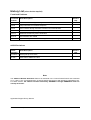
Microcontroller Components
Errata Sheet
October 2, 1998 / Release 1.1
Device:
Stepping Code / Marking:
Package:
SAB-C161V-L16M
AA
MQFP-80
This Errata Sheet describes the deviations from the current user documentation. The
classification and numbering system is module oriented in a continual ascending sequence
over several derivatives, as well already solved deviations are included. So gaps inside this
enumeration could occur.
The current documentation is: Data Sheet: C161V/C161K/C161O Data Sheet 03.97,
User’s Manual: C161V/C161K/C161O User’s Manual 12.96,
Version 1.0
Instruction Set Manual 12.97 Version 1.2
Note: Devices marked with EES- or ES are engineering samples which may not be
completely tested in all functional and electrical characteristics, therefore they should
be used for evaluation only.
The specific test conditions for EES and ES are documented in a separate Status Sheet.
Change summary to Errata Sheet Rel.1.0 for devices with stepping code/marking AA:
•
•
•
•
•
•
•
PEC Transfers after JMPR (BUS.18)
Arithmetic Overflow by DIVLU instruction (CPU.17)
System Configuration via P0L.0 during Software/Watchdog Timer Reset (RST.1)
new naming convention for DC/AC specification deviations used
Limit for timing t6 (address setup to ALE) changed from TCL-15 to TCL-17.5ns (AC.t6.1)
Limit for timing t22 (data valid to WR#) changed from 2TCL-15 to 2TCL-20ns (AC.t22.1)
Note about Address Window Arbitration added (see end of document)
Semiconductor Group
Errata Sheet, C161V-L16M, AA, 1.1, Mh
- 1 of 8 -
Functional Problems:
CPU.17:
Arithmetic Overflow by DIVLU instruction
For specific combinations of the values of the dividend (MDH, MDL) and divisor (Rn), the Overflow (V)
flag in the PSW may not be set for unsigned divide operations, although an overflow occurred.
E.g.:
MDH
F0F0
MDL
Rn
MDH MDL
0F0Fh : F0F0h = FFFF FFFFh, but no Overflow indicated!
(result with 32-bit precision: 1 0000h)
The same malfunction appears for the following combinations:
n0n0 0n0n : n0n0
n00n 0nn0 : n00n
n000 000n : n000
n0nn 0nnn : n0nn
where n means any Hex Digit between 8 ... F
i.e. all operand combinations where at least the most significant bit of the dividend (MDH) and the
divisor (Rn) is set.
In the cases where an overflow occurred after DIVLU, but the V flag is not set, the result in MDL is
equal to FFFFh.
Workaround:
Skip execution of DIVLU in case an overflow would occur, and explicitly set V = 1.
E.g.:
CMP Rn, MDH
JMPR cc_ugt, NoOverflow
; no overflow if Rn > MDH
BSET V
; set V = 1 if overflow would occur
JMPR cc_uc, NoDivide
; and skip DIVLU
NoOverflow:
DIVLU Rn
NoDivide:
...
; next instruction, may evaluate correct V flag
Note:
- the KEIL C compiler, run time libraries and operating system RTX166 do not generate or use
instruction sequences where the V flag in the PSW is tested after a DIVLU instruction.
- with the TASKING C166 compiler, for the following intrinsic functions code is generated which uses
the overflow flag for minimizing or maximizing the function result after a division with a DIVLU:
_div_u32u16_u16()
_div_s32u16_s16()
_div_s32u16_s32()
Consequently, an incorrect overflow flag (when clear instead of set) might affect the result of one of the
above intrinsic functions but only in a situation where no correct result could be calculated anyway.
These intrinsics first appeared in version 5.1r1 of the toolchain.
Libraries: not affected
Semiconductor Group
Errata Sheet, C161V-L16M, AA, 1.1, Mh
- 2 of 8 -
CPU.11:
Stack Underflow Trap during Restart of interrupted Multiply
Wrong multiply results may be generated when a STUTRAP (stack underflow) is caused by the last
implicit stack access (= pop PSW) of a RETI instruction which restarts an interrupted MUL/MULU
instruction.
No problem will occur in systems where the stack overflow/underflow detection is not used, or where
an overflow/underflow will result in a system reset.
Workaround 1:
Avoid a stack overflow/underflow e.g. by
- allocating a larger internal system stack (via bitfield STKSZ in register SYSCON), or
- reducing the required stack space by reducing the number of interrupt levels, or
- testing in each task procedure whether a stack underflow is imminent, and anticipating the stack refill
procedure before executing the RETI instruction.
Workaround 2:
Disable MULx instructions from being interrupted e.g. with the following instruction sequence:
ATOMIC #1
MULx Rm, Rn
Workaround 3 (may be selected if no divide operations are used in an interruptible program section):
In each interrupt service routine (task procedure), always clear bit MULIP in the PSW and set register
MDC to 0000h. This will cause an interrupted multiplication to be completely restarted from the first
cycle after return to the priority level on which it was interrupted.
In case that an interrupt service routine is also using multiplication, only registers MDH and MDL must
be saved/restored when using this workaround, while bit MULIP and register MDC must be set to zero.
CPU.9:
PEC Transfers during instruction execution from Internal RAM
When a PEC transfer occurs after a jump with cache hit during instruction execution from internal RAM
(locations 0FA00h - 0FDFFh), the instruction following the jump target instruction may not be (correctly)
executed. This problem occurs when the following sequence of conditions is true:
i)
a loop terminated with a jump which can load the jump target cache (possible for JMPR, JMPA,
JB, JNB, JBC, JNBS) is executed in the internal RAM
ii)
at least two loop iterations are performed, and no JMPS, CALLS, RETS, TRAP, RETI
instruction or interrupt is processed between the last and the current iteration through the loop
(i.e. the condition for a jump cache hit is true)
iii)
a PEC transfer is performed after the jump at the end of the loop has been executed
iv)
the jump target instruction is a double word instruction
Workaround 1:
Place a single word instruction (e.g. NOP) at the jump target address in the internal RAM.
Workaround 2:
Use JMPS (unconditional) or JMPI (conditional) instructions at the end of the loop in the internal RAM.
These instructions will not use the jump cache.
Semiconductor Group
Errata Sheet, C161V-L16M, AA, 1.1, Mh
- 3 of 8 -
CPU.8:
Jump instructions in EXTEND sequence
When a jump or call is taken in an EXTS, EXTSR, EXTP, or EXTPR sequence, a following data access
included in the EXTEND sequence might be performed to a wrong segment or page number.
Note: ATOMIC or EXTR sequences are not affected by this problem.
Example: Accessing double-word data with a check on segment overflow between the two accesses
(R5 contains 8-bit segment number, R4 contains 16-bit intra-segment offset address):
EXTS R5,#4
; start EXTEND sequence
MOV R10,[R4+]
; get first word
CMP R4,#0
; check for segment overflow
JMPR cc_NZ,Next
; jump if no segment overflow
ADD R5,#1
; increment to next segment
EXTS R5,#1
; continue EXTEND sequence
Next: MOV R11,[R4]
; get second word
With this sequence, the problem can occur when the jump is taken to label Next; the data access here
might use a wrong segment number.
Workaround:
Do not use jumps or calls in EXTS, EXTSR, EXTP, or EXTPR sequences. This can be done very easily
since only an actual data access must be included in an EXTEND sequence. All other instructions,
such as comparisons and jumps, do not necessarily have to be in the EXTEND sequence.
For the example shown above, there are several possibilities to get around the problem:
a) with a jump, but EXTEND sequence only for the data accesses
Next:
EXTS
MOV
CMP
JMPR
ADD
EXTS
MOV
R5,#1
R10,[R4+]
R4,#0
cc_NZ,Next
R5,#1
R5,#1
R11,[R4]
; EXTEND sequence only for data access
; get first word
; check for segment overflow
; jump if no segment overflow
; increment to next segment
; second EXTEND sequence for data access
; get second word
b) without a jump
EXTS
MOV
ADD
ADDC
EXTS
MOV
R5,#4
R10,[R4]
R4,#2
R5,#0
R5,#1
R11,[R4]
; EXTEND sequence
; get first word
; increment pointer here
; add possible overflow from pointer inc.
; continue EXTEND sequence
; get second word
The first EXTEND instruction of example b) can also be modified such that only the following data
access is included in the EXTEND sequence (EXTS R5,#1). This additionally has the effect of a
reduced interrupt latency.
Notes on Compilers and Operating Systems
Such critical sequences might be produced within library functions of C-Compilers when accessing
huge double-word data, or in operating systems. From the following compiler versions, we currently
know that they are not affected by this problem:
BSO/Tasking V4.0r3
HighTec C16x-GNU-C V3.1
Keil C166 (from V2.60)
Semiconductor Group
Errata Sheet, C161V-L16M, AA, 1.1, Mh
- 4 of 8 -
CPU.7:
Warm HW Reset (Pulse Length < 1032 TCL)
In case a HW reset signal with a length < 1032 TCL (25.8 µs @ 20 MHz) is applied to pin RSTIN#, the
internal reset sequence may be terminated before the specified time of 1032 TCL, and not all SFRs
and ESFRs may be correctly reset to their default state. Instead, they maintain the state which they
had before the falling edge of RSTIN#. The problem occurs when the falling edge of the
(asynchronous) external RSTIN# signal is coincident with a specific internal state of the controller. The
problem will statistically occur more frequently when waitstates are used on the external bus.
Workaround:
Extend the HW reset signal at pin RSTIN# (e.g. with an external capacitor) such that it stays below V IL
(0.2 Vcc - 0.1 V) for at least 1032 TCL.
BUS.18:
PEC Transfers after JMPR instruction
Problems may occur when a PEC transfer immediately follows a taken JMPR instruction when the
following sequence of 4 conditions is met (labels refer to following examples):
1. in an instruction sequence which represents a loop, a jump instruction (Label_B) which is capable
of loading the jump cache (JMPR, JMPA, JB/JNB/JBC/JNBS) is taken
2. the target of this jump instruction directly is a JMPR instruction (Label_C) which is also taken and
whose target is at address A (Label_A)
3. a PEC transfer occurs immediately after this JMPR instruction (Label_C)
4. in the following program flow, the JMPR instruction (Label_C) is taken a second time, and no other
JMPR, JMPA, JB/JNB/JBC/JNBS or instruction which has branched to a different code segment
(JMPS/CALLS) or interrupt has been processed in the meantime (i.e. the condition for a jump
cache hit for the JMPR instruction (Label_C) is true)
In this case, when the JMPR instruction (Label_C) is taken for the second time (as described in
condition 4 above), and the 2 words stored in the jump cache (word address A and A+2) have been
processed, the word at address A+2 is erroneously fetched and executed instead of the word at
address A+4.
Note: the problem does not occur when the jump instruction (Label_C) is a JMPA instruction
Example1:
Label_A: instruction x
; Begin of Loop
instruction x+1
.....
Label_B: JMP Label_C ; JMP may be any of the following jump instructions:
JMPR cc_zz, JMPA cc_zz, JB/JNB/JBC/JNBS
; jump must be taken in loop iteration n
; jump must not be taken in loop iteration n+1
.....
Label_C: JMPR cc_xx, Label_A
; End of Loop
; instruction must be JMPR (single word instruction)
; jump must be taken in loop iteration n and n+1
; PEC transfer must occur in loop iteration n
Semiconductor Group
Errata Sheet, C161V-L16M, AA, 1.1, Mh
- 5 of 8 -
Example2:
Label_A: instruction x
; Begin of Loop1
instruction x+1
.....
Label_C: JMPR cc_xx, Label_A
; End of Loop1, Begin of Loop2
; instruction must be JMPR (single word instruction)
; jump not taken in loop iteration n-1, i.e. Loop2 is entered
; jump must be taken in loop iteration n and n+1
; PEC transfer must occur in loop iteration n
.....
Label_B: JMP Label_C
; End of Loop2
; JMP may be any of the following jump instructions:
JMPR cc_zz, JMPA cc_zz, JB/JNB/JBC/JNBS
; jump taken in loop iteration n-1
A code sequence with the basic structure of Example1 was generated e.g. by a compiler for
comparison of double words (long variables).
Workarounds:
1. use a JMPA instruction instead of a JMPR instruction when this instruction can be the direct target
of a preceding JMPR, JMPA, JB/JNB/JBC/JNBS instruction, or
2. insert another instruction (e.g. NOP) as branch target when a JMPR instruction would be the direct
target of a preceding JMPR, JMPA, JB/JNB/JBC/JNBS instruction, or
3. change the loop structure such that instead of jumping from Label_B to Label_C and then to
Label_A, the jump from Label_B directly goes to Label_A.
Notes on compilers:
In the Hightec compiler beginning with version Gcc 2.7.2.1 for SAB C16x – V3.1 Rel. 1.1, patchlevel 5,
a switch –m bus18 is implemented as workaround for this problem. In addition, optimization has to be
set at least to level 1 with –u1.
The Keil C compiler and run time libraries do not generate or use instruction sequences where a JMPR
instruction can be the target of another jump instruction, i.e. the conditions for this problem do not
occur.
Other compilers under evaluation.
RST.1:
System Configuration via P0L.0 during Software/Watchdog
Timer Reset
Unlike P0L.5 .. P0L.1, P0L.0 is not disregarded during software or watchdog timer reset. This
means that when P0L.0 is (erroneously) externally pulled low at the end of the internal software or
watchdog timer reset sequence, the device will enter emulation mode.
Therefore, ensure that the level at P0L.0 is above the minimum input high voltage VIHmin= 0.2 Vcc + 0.9
V (1.9 V @ Vcc = 5.0 V) at the end of the internal reset sequence.
Semiconductor Group
Errata Sheet, C161V-L16M, AA, 1.1, Mh
- 6 of 8 -
Deviations from Electrical- and Timing Specification:
The following table lists the deviations of the DC/AC characteristics from the specification in the
C161V/C161K/C161O Data Sheet 03.97
3UREOHP
3DUDPHWHU
6\PERO
/LPLW 9DOXHV
VKRUW QDPH
DC.RRST.1
RSTIN# pull-up
Problem
Parameter
short name
RRST
Symbol
8QLW
min.
max.
25
instead of
50
125
instead of
150
Max. CPU Clock
= 16 MHz
7HVW
&RQGLWLRQ
kΩ
Variable CPU Clock Unit
1/2TCL = 1 to 16 MHz
min.
max.
min.
AC.t6.1
Address setup to
ALE
t6
13.5+ta
instead of
16+ta
-
TCL-17.5+ta instead of
TCL-15+ta
max.
ns
AC.t22.1
Data valid to WR#
t22
43+tc
instead of
48+tc
-
2TCL-20+tc
instead of
2TCL-15+tc
ns
-
Notes:
1) Timing t28: Parameter description and test changed from ’Address hold after RD#/WR#’ to ’Address
hold after WR#’. It is guaranteed by design that read data are internally latched by the controller before
the address changes.
2) During reset, the port 6 lines P6.[3:0] are pulled high by internal pull-ups.
Semiconductor Group
Errata Sheet, C161V-L16M, AA, 1.1, Mh
- 7 of 8 -
History List (since device step AA)
Functional Problems
Functional Short Description
Problem
Fixed in
step
CPU.7
Warm hardware reset (pulse length < 1032 TCL)
CPU.8
Jump instructions in EXTEND sequence
CPU.9
PEC Transfers during instruction execution from Internal RAM
CPU.11
Stack Underflow Trap during restart of interrupted Multiplication
CPU.17
Arithmetic Overflow by DIVLU instruction
BUS.18
PEC transfers after JMPR
RST.1
System Configuration via P0L.0 during Software/Watchdog Timer Reset
AC/DC Deviations
AC/DC
Deviation
Short Description
Fixed in
step
DC.RRST.1 RSTIN pull-up 25 to 125 kΩ
AC.t22.1
Data valid to WR# 2TCL-20ns
Note
The Address Window Arbitration feature as described in the C161V/C161K/C161O User’s Manual
V1.0, p.8-21 is not yet implemented in C161V/C161K/C161O devices with stepping code/marking AA.
For these devices, the address windows defined by ADDRSEL1 through ADDRSEL4 must not
overlap each other.
Application Support Group, Munich
Semiconductor Group
Errata Sheet, C161V-L16M, AA, 1.1, Mh
- 8 of 8 -