1
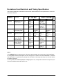
Microcontroller Components
Errata Sheet
November 3, 1998 / Release 1.0
Device:
Stepping Code / Marking:
Package:
SAB-C163-LF
SAB-C163-L25F
SAF-C163-L25F
AC
TQFP-100
This Errata Sheet describes the deviations from the current user documentation. The
classification and numbering system is module oriented in a continual ascending sequence
over several derivatives, as well already solved deviations are included. So gaps inside this
enumeration could occur.
The current documentation is: Data Sheet: C163-L Data Sheet 1998-08
User’s Manual: C165/C163 User’s Manual V2.0 10.96
Instruction Set Manual 12.97 Version 1.2
Note: Devices marked with EES- or ES are engineering samples which may not be
completely tested in all functional and electrical characteristics, therefore they should
be used for evaluation only.
The specific test conditions for EES and ES are documented in a separate Status Sheet.
Change summary to Errata Sheet Rel.1.2 for devices with stepping code/marking AB:
•
•
•
•
•
Problem CPU.11 (Stack Underflow Trap during Restart of interrupted Multiply) fixed
Problem RST.1 (System Configuration via P0L.0 during Software/Watchdog Timer Reset) fixed
PEC Transfers after JMPR (BUS.18): note about TASKING software development tools
added
Read Access to XPERs in Visible Mode (X9): description modified
Note on Pin OWE (Oscillator Watchdog Enable) added (see end of document)
Semiconductor Group
Errata Sheet, C163-L(25)F, AC, 1.0, Mh
- 1 of 8 -
Functional Problems:
CPU.17:
Arithmetic Overflow by DIVLU instruction
For specific combinations of the values of the dividend (MDH, MDL) and divisor (Rn), the Overflow (V)
flag in the PSW may not be set for unsigned divide operations, although an overflow occurred.
E.g.:
MDH
F0F0
MDL
Rn
MDH MDL
0F0Fh : F0F0h = FFFF FFFFh, but no Overflow indicated!
(result with 32-bit precision: 1 0000h)
The same malfunction appears for the following combinations:
n0n0 0n0n : n0n0
n00n 0nn0 : n00n
n000 000n : n000
n0nn 0nnn : n0nn
where n means any Hex Digit between 8 ... F
i.e. all operand combinations where at least the most significant bit of the dividend (MDH) and the
divisor (Rn) is set.
In the cases where an overflow occurred after DIVLU, but the V flag is not set, the result in MDL is
equal to FFFFh.
Workaround:
Skip execution of DIVLU in case an overflow would occur, and explicitly set V = 1.
E.g.:
CMP Rn, MDH
JMPR cc_ugt, NoOverflow
; no overflow if Rn > MDH
BSET V
; set V = 1 if overflow would occur
JMPR cc_uc, NoDivide
; and skip DIVLU
NoOverflow:
DIVLU Rn
NoDivide:
...
; next instruction, may evaluate correct V flag
Note:
- the KEIL C compiler, run time libraries and operating system RTX166 do not generate or use
instruction sequences where the V flag in the PSW is tested after a DIVLU instruction.
- with the TASKING C166 compiler, for the following intrinsic functions code is generated which uses
the overflow flag for minimizing or maximizing the function result after a division with a DIVLU:
_div_u32u16_u16()
_div_s32u16_s16()
_div_s32u16_s32()
Consequently, an incorrect overflow flag (when clear instead of set) might affect the result of one of the
above intrinsic functions but only in a situation where no correct result could be calculated anyway.
These intrinsics first appeared in version 5.1r1 of the toolchain.
Libraries: not affected
Semiconductor Group
Errata Sheet, C163-L(25)F, AC, 1.0, Mh
- 2 of 8 -
PWRDN.1:
Execution of PWRDN Instruction while pin NMI# = high
When instruction PWRDN is executed while pin NMI# is at a high level, power down mode should not
be entered, and the PWRDN instruction should be ignored. However, under the conditions described
below, the PWRDN instruction may not be ignored, and no further instructions are fetched from
external memory, i.e. the CPU is in a quasi-idle state. This problem will only occur in the following
situations:
a) the instructions following the PWRDN instruction are located in external memory, and a multiplexed
bus configuration with memory tristate waitstate (bit MTTCx = 0) is used, or
b) the instruction preceding the PWRDN instruction writes to external memory or an XPeripheral (SSP
module), and the instructions following the PWRDN instruction are located in external memory. In
this case, the problem will occur for any bus configuration.
Note: the on-chip peripherals are still working correctly, in particular the Watchdog Timer will reset the
device upon an overflow. Interrupts and PEC transfers, however, can not be processed. In case NMI#
is asserted low while the device is in this quasi-idle state, power down mode is entered.
Workaround:
Ensure that no instruction which writes to external memory or an XPeripheral precedes the PWRDN
instruction, otherwise insert e.g. a NOP instruction in front of PWRDN. When a muliplexed bus with
memory tristate waitstate is used, the PWRDN instruction should be executed out of internal RAM.
BUS.18:
PEC Transfers after JMPR instruction
Problems may occur when a PEC transfer immediately follows a taken JMPR instruction when the
following sequence of 4 conditions is met (labels refer to following examples):
1. in an instruction sequence which represents a loop, a jump instruction (Label_B) which is capable
of loading the jump cache (JMPR, JMPA, JB/JNB/JBC/JNBS) is taken
2. the target of this jump instruction directly is a JMPR instruction (Label_C) which is also taken and
whose target is at address A (Label_A)
3. a PEC transfer occurs immediately after this JMPR instruction (Label_C)
4. in the following program flow, the JMPR instruction (Label_C) is taken a second time, and no other
JMPR, JMPA, JB/JNB/JBC/JNBS or instruction which has branched to a different code segment
(JMPS/CALLS) or interrupt has been processed in the meantime (i.e. the condition for a jump
cache hit for the JMPR instruction (Label_C) is true)
In this case, when the JMPR instruction (Label_C) is taken for the second time (as described in
condition 4 above), and the 2 words stored in the jump cache (word address A and A+2) have been
processed, the word at address A+2 is erroneously fetched and executed instead of the word at
address A+4.
Note: the problem does not occur when the jump instruction (Label_C) is a JMPA instruction
Semiconductor Group
Errata Sheet, C163-L(25)F, AC, 1.0, Mh
- 3 of 8 -
Example1:
Label_A: instruction x
; Begin of Loop
instruction x+1
.....
Label_B: JMP Label_C ; JMP may be any of the following jump instructions:
JMPR cc_zz, JMPA cc_zz, JB/JNB/JBC/JNBS
; jump must be taken in loop iteration n
; jump must not be taken in loop iteration n+1
.....
Label_C: JMPR cc_xx, Label_A
; End of Loop
; instruction must be JMPR (single word instruction)
; jump must be taken in loop iteration n and n+1
; PEC transfer must occur in loop iteration n
Example2:
Label_A: instruction x
; Begin of Loop1
instruction x+1
.....
Label_C: JMPR cc_xx, Label_A
; End of Loop1, Begin of Loop2
; instruction must be JMPR (single word instruction)
; jump not taken in loop iteration n-1, i.e. Loop2 is entered
; jump must be taken in loop iteration n and n+1
; PEC transfer must occur in loop iteration n
.....
Label_B: JMP Label_C
; End of Loop2
; JMP may be any of the following jump instructions:
JMPR cc_zz, JMPA cc_zz, JB/JNB/JBC/JNBS
; jump taken in loop iteration n-1
A code sequence with the basic structure of Example1 was generated e.g. by a compiler for
comparison of double words (long variables).
Workarounds:
1. use a JMPA instruction instead of a JMPR instruction when this instruction can be the direct target
of a preceding JMPR, JMPA, JB/JNB/JBC/JNBS instruction, or
2. insert another instruction (e.g. NOP) as branch target when a JMPR instruction would be the direct
target of a preceding JMPR, JMPA, JB/JNB/JBC/JNBS instruction, or
3. change the loop structure such that instead of jumping from Label_B to Label_C and then to
Label_A, the jump from Label_B directly goes to Label_A.
Notes on compilers:
In the Hightec compiler beginning with version Gcc 2.7.2.1 for SAB C16x – V3.1 Rel. 1.1, patchlevel 5,
a switch –m bus18 is implemented as workaround for this problem. In addition, optimization has to be
set at least to level 1 with –u1.
The Keil C compiler and run time libraries do not generate or use instruction sequences where a JMPR
instruction can be the target of another jump instruction, i.e. the conditions for this problem do not
occur.
In the TASKING C166 Software Development Tools, the code sequence related to problem BUS.18
can be generated in Assembly. The problem can also be reproduced in C-language by using a
particular sequence of GOTOs.
With V6.0r3, TASKING tested all the Libraries, C-startup code and the extensive set of internal testsuite sources and the BUS.18 related code sequence appeared to be NOT GENERATED.
Semiconductor Group
Errata Sheet, C163-L(25)F, AC, 1.0, Mh
- 4 of 8 -
To prevent introduction of this erroneous code sequence, the TASKING Assembler V6.0r3 has been
extended with the CHECKBUS18 control which generates a WARNING in the case the described code
sequence appears. When called from within EDE, the Assembler control CHECKBUS18 is
automatically ’activated’.
X9:
Read Access to XPERs in Visible Mode
The data of a read access to an XBUS-Peripheral (SSP) in Visible Mode is not driven to the external
bus. PORT0 is tristated during such read accesses.
Note that in Visible Mode PORT1 will drive the address for an access to an XBUS-Peripheral, even
when only a multiplexed external bus is enabled.
X12:
P0H spikes after XPER write access and external 8-bit Non-multiplexed bus
When an external 8-bit non-multiplexed bus mode is selected and P0H is used for general purpose I/O,
and an internal (byte or word) write access to an XBUS peripheral (SSP module) is performed, and an
external bus cycle is directly following the internal XBUS write cycle, then P0H is actively driven with
the write data for approx. 7ns (spikes on P0H).
The spikes also occur if P0H is configured as input. However, read operations from P0H are not
affected and will always return the correct logical state.
The spikes have the following position and shape in a typical application:
spikes occur after the rising edge of CLKOUT which follows the rising edge of ALE for the external bus
cycle
P0H.x = low
--> output low voltage rises to approx. 2.5V, spike width approx. 7ns (@ 0.2 Vcc)
P0H.x = high --> output high voltage drops to approx. 2.0V, spike width approx. 7ns (@ 0.8 Vcc)
Referring to a worst case simulation the maximum width of the spikes may be 15ns with full amplitude
(Vcc/Vss). But this might not be seen on application level.
Note that if any of the other bus modes is selected in addition to the 8-bit non-multiplexed mode, P0H
can not be used for I/O per default.
Workaround:
-
use a different port instead of P0H for I/O when (only) an external 8-bit non-multiplexed bus mode
is selected
or use a different bus type (e.g. 8-bit multiplexed, where P1H may be used for I/O instead of P0H)
or the spikes on P0H may be filtered with an application specific RC element,
or do not perform an external bus access directly after an XBUS write access:
this may be achieved by an instruction sequence which is executed in internal RAM
e.g.
ATOMIC #3
; to prevent PEC transfers which may access external memory
instruction which writes to XBUS peripheral
NOP
NOP
Semiconductor Group
Errata Sheet, C163-L(25)F, AC, 1.0, Mh
- 5 of 8 -
Deviations from Electrical- and Timing Specification:
The following table lists the deviations of the DC/AC characteristics from the specification in the C163-L
Data Sheet 1998-08.
Problem
Parameter
short name
Symbol Max. CPU Clock
= 25 MHz
min.
max.
Variable CPU Clock Unit
1/2TCL = 1 to 25 MHz
min.
max.
AC.t13.2
RD#/WR# low time
(no RW-delay)
t13
45+tc
instead of
50+tc
3TCL-15+tc instead of
3TCL –10+tc
ns
AC.t22.2
Data valid to WR#
t22
18+tc
instead of
20+tc
2TCL-22+tc
instead of
2TCL-20+tc
-
ns
AC.t34.1
CLKOUT rising edge t34
to ALE falling edge
0+ta
12+ta
instead of
10+ta
ns
AC.t38.3
ALE falling edge to
CS#
t38
-6-ta
4-ta
-6-ta
instead of instead of instead of
-4-ta
10-ta
-4-ta
4-ta
instead of
10-ta
ns
AC.t42.1
ALE falling edge to
RDCS#, WRCS#
(with R/W Delay)
t42
14+ta
instead of
16+ta
TCL-6+ta
instead of
TCL-4+ta
-
ns
AC.t43.1
ALE falling edge to
RDCS#, WRCS#
(no R/W Delay)
t43
-6+ta
instead of
-4+ta
-6+ta
-
ns
22+tc
instead of
26+tc
2TCL-18+tc
instead of
2TCL-14+tc
-
ns
AC.t50.1
Data valid to WRCS# t50
12+ta
0+ta
instead of
10+ta
instead of
-4+ta
Notes:
1) Pin READY# has an internal pull-up. This will be documented in the next revision of the Data Sheet.
2) Timing t28: Parameter description and test changed from 'Address hold after RD#/WR#' to 'Address
hold after WR#'. It is guaranteed by design that read data are internally latched by the controller before
the address changes.
3) During reset, the internal pull-ups on P6.[4:0] are active, independent whether the respective pins
are used for CS# function after reset or not.
Semiconductor Group
Errata Sheet, C163-L(25)F, AC, 1.0, Mh
- 6 of 8 -
History List (since device step AA)
Functional Problems
Functional Short Description
Problem
Fixed in
step
CPU.11
Stack Underflow Trap during restart of interrupted Multiplication
CPU.17
Arithmetic Overflow by DIVLU instruction
BUS.18
PEC transfers after JMPR
INT.8
Interrupt Generation during Cache Hit
PWRDN.1
Execution of PWRDN Instruction while pin NMI# = high
RST.1
System Configuration via P0L.0 during Software/Watchdog Timer Reset
X9
Read Access to XPERs in Visible Mode
X12
P0H spikes after XPER write access and external 8-bit Non-multiplexed bus
AC
AB
AC
AC/DC Deviations
AC/DC
Deviation
Short Description
AC.t13.2
RD#/WR# low time (no RW-delay) 3TCL-15ns
AC.t22.2
Data valid to WR# 2TCL-22ns
AC.t34.1
CLKOUT rising edge to ALE falling edge 12+ta ns
AC.t38.3
ALE falling edge to CS# -6/+4ns
AC.t42.1
ALE falling edge to RDCS#, WRCS# (with R/W Delay) TCL-6ns
AC.t43.1
ALE falling edge to RDCS#, WRCS# (no R/W Delay) –6ns
AC.t50.1
Data valid to WRCS# 2TCL-18ns
Semiconductor Group
Fixed in
step
Errata Sheet, C163-L(25)F, AC, 1.0, Mh
- 7 of 8 -
Note on pin OWE (Oscillator Watchdog Enable)
During direct drive or prescaler operation the Oscillator Watchdog (OWD) may be used to monitor the
clock signal generated by the on-chip oscillator (either with a crystal or via external clock drive). For this
operation the OWD uses the PLL clock signal to supervise transitions on the oscillator clock. As the
PLL does not generate the CPU clock signal, it is disconnected from the oscillator clock and delivers its
base frequency.
A low level on pin OWE disables the Oscillator Watchdog. In this case, also the PLL is disabled to
reduce power consumption. An internal pull-up is implemented on pin OWE.
For 3 V operation (reduced supply voltage range) pin OWE must always be low (i.e. OWD disabled)
as the PLL cannot deliver an appropriate clock signal in this case. Only direct drive (P0H.[7:5] = 011
during reset) or prescaler operation (P0H.[7:5] = 001) is possible in this case.
For 5 V operation (standard supply voltage range) pin OWE should only be pulled low (i.e. PLL
disabled) when direct drive or prescaler operation is configured.
For all other combinations the PLL is configured to generate the CPU clock signal and therefore should
not be disabled by a low level on pin OWE. PLL configurations with OWE = low result either in direct
drive operation (when P0H.7 = high) or prescaler operation (when P0H.7 = low).
Previous steps of the C163-L (e.g. AB-step) in this case did not switch off the PLL, i.e. they would still
multiply the clock supplied on XTAL1 to generate the internal CPU clock fcpu.
Application Support Group, Munich
Semiconductor Group
Errata Sheet, C163-L(25)F, AC, 1.0, Mh
- 8 of 8 -