1
TWIMO HP & MP Modules
RTU & API
User’s guide
TWIMO_Module_V1.4_user_guide
Table of contents
TWIMO REGULATORY CONSIDERATIONS
4
1.TWIMO module range
1.1. Form factor and footprint
1.2. Module’s hardware architecture
1.3. Technical Specifications
1.4. Hardware integration
1.5. Antenna 1.6. Power Supply
5
5
6
6
7
7
8
2.TWIMO concept
2.1. “Ready to Use” version: configurable RF gateway
2.2. “Programmable” version: embedding your application in it!
9
9
9
3.“Ready To Use” version
3.1. Operating modes
3.1.1Command Mode
3.1.2Communication mode
3.1.2.01
Asynchronous mode of communication
3.1.2.02
Synchronous (TDMA) mode of communication
3.1.2.03
Synchronous vs Asynchronous (drawback and advantage)
3.2. Command Interface
3.2.1Entering Command Mode
3.2.1.01
Through the RS232 serial link
3.2.1.02
Through a dedicated pin of the module (pin n° 8: Cmd_Mode): 3.2.2AT Commands 3.2.2.01
AT Commands : module configuration
3.2.2.02
AT Commands : module test
3.2.3Register parameter
3.2.4Default settings
3.3. Communication mode: Sending and Receiving datas
3.3.1Modem state machine
3.3.2Data flow
3.3.3Packet format
3.3.4Addressing modes
3.3.4.01
Transparent mode 3.3.4.02
Addressed mode
3.3.5Receiving mode
3.3.6LED Status
3.3.7Synchronous TDMA mode
3.4. Radio characteristics
3.4.1Narrow band system
3.4.2Medium band system
3.4.3Wide band system
3.4.4Summary
9
9
10
10
10
10
11
11
11
11
12
12
12
12
13
14
14
15
15
15
16
16
17
17
17
17
18
18
18
18
18
4.Firmware upgrade
19
5.“Programmable” version
5.1. API concept
20
20
TWIMO_Module_V1.4_user_guide
5.2. Hardware Interface description
5.2.1Pin Description
5.3. Resources availability and partitioning
5.3.1Flash memory
5.3.2RAM memory
5.3.3E2PROM memory
5.3.4TWIMO firmware requirement in terms of memory
5.3.5Peripheral (GPIO, ADC/DAC, Communication etc…)
5.3.6Hardware Timer
5.3.7DMA
5.3.8GPIO Interrupt line and vectors
5.3.9Interrupt vector priority 5.3.10 CPU Frequency
5.4. API TWIMO
5.4.1Radio related APIs
5.4.1.01TWIMO_API_SystemInit()
5.4.1.02TWIMO_API_Radio_BackgroundTask()
5.4.1.03
TWIMO_API_Radio_SendData ()
5.4.1.04TWIMO_API_Radio_ReceiveData()
5.4.1.05TWIMO_API_GetFirmwareVersion()
5.4.2TWIMO API data structure
5.4.2.01TWIMO_INIT
5.4.2.02TWIMO_RADIO_TX
5.4.2.03TWIMO_RADIO_RX
5.4.3TWIMO firmware operating
5.4.4Application Template
5.5. TWIMO API: how to use it ?
5.6. Code Integration
5.6.1Application background task execution
5.6.2Application interrupt execution
5.6.3Miscellaneous
5.7. Compiling code
5.7.1Code Generation tool
5.7.2Project/Workspace exemple
5.8. Bootloading
6.Process
6.1. Description of module 7581-A and board ARF7628/B
6.2. BOM analysis
6.3. Risk linked to number of reflows
6.4. Risk Management for Moisture sensitivity
6.5. Soldering curve
TWIMO_Module_V1.4_user_guide
21
21
21
21
21
22
22
22
22
23
23
24
24
25
25
25
25
26
26
27
27
27
29
29
30
31
31
32
32
32
32
32
32
33
33
33
33
34
34
36
37
TWIMO REGULATORY CONSIDERATIONS
Ready to Use” versions ARF7580AA & ARF 7581AA
DECLARATION OF CONFORMITY (CE0081)
We ADEUNIS RF
283 rue LOUIS NEEL
38920 CROLLES FRANCE
declare under our own responsibility that the TWIMO modules ARF7580AA&ARF7581AA to which this declaration refers conforms with the relevant standards or other standardising documents:
• EN 300 220-2 (v2.1.2) (2007-06)
• EN 300 220-2 (V2.3.1) (2010-02)
• EN 60950-1 (2001) + A11 (2004)
• EN50371 (2002) / EN62311 (2008) / EN50385 (2008)
• EN301 489-1 (v1.8.1) (2008-04)
• EN 301 489-3 (v1.4.1) (2002-08)
• EN 62311 (2008)
According to the RTTE Directive 99/5/EC
Notes:
• Conformity has been evaluated according to the procedure described in Annex IV of the RTTE directive
(Statement of opinion from a notify body N°102158-604317-1/2)
•
Conformity has been evaluated with ARF7580AA module integrated on ADEUNIS RF TWIMO Starter Kit
ARF7659B and with ARF7581AA module integrated on ADEUNIS RF TWIMO Starter Kit ARF7659C.
• According to the 1999/519/EC «RF signal» recommendations, a minimum distance of 10cm between the
product and the body is required.
• Receiver class (if applicable): 2
RTTE COMPLIANT END PRODUCT
To get a RTTE COMPLIANT END PRODUCT with the ready to use version, user or integrator must follow the
integration proposed in the ADEUNIS RF TWIMO SK ARF7659B or ARF7659C. Please have a look on the
TWIMO SK user guide (www.adeunis-rf.com) for information about schematics, PCB, battery, antenna, software
version…
If one of the conditions described in the SK user guide is not respected or is modified, additional normative
tests will be necessary on the end product to ensure the RTTE conformity. As the integration of a radio module
requires wireless technological knowledge, ADEUNIS RF proposes its technical proficiency to its customers for a
pre-compliance qualification of end products.
If the software of the module is changed or modified, the module becomes a programmable version and looses
the CE conformity.
PROGRAMMABLE” versions ARF7734 / ARF7735 / ARF7736
For these versions, the RF behavior of the product and of the module will among others depend on the software
included by the user or integrator in the module. Thus :
•
•
There is no sense to speak about CE conformity of the module
The RTTE conformity of the end product shall have to be evaluated with the module integrated the final
software.
According the customer software, conformity of the end product shall be evaluated case by case. Moreover, as
the integration of a radio module requires wireless technological knowledge, ADEUNIS RF proposes its technical
proficiency to its customers for a pre-compliance qualification of end products
TWIMO_Module_V1.4_user_guide
4
1.TWIMO module range
1.1. Form factor and footprint
The TWIMO range is made up of 3 modules.
• High Power Module (HP) : able to deliver up to 500 mW (27 dBm) output power
• Medium Power module (MP): able to deliver up to 50 mW (17 dBm) output power
• Low Power Module (LP): able to deliver up to 10 mW (10 dBm) output power
This document deals only with the HP and MP modules.
The 2 modules are pin-to-pin compatible.
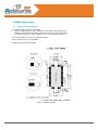
Footprint of the MP and HP modules:
Figure 1. Module’s footprint
TWIMO_Module_V1.4_user_guide
5
Pinout of the modules:
Figure 2. Module’s pinout
The description and the functionalities associated with each pin are described further in this document.
1.2.
Module’s hardware architecture
The modules are made up of 2 parts:
• 1 “Digital” part which mainly consist of a microcontroller belonging to the STM32F101x family.
• 1 “Radio” part which mainly consists of a radio chip (SX1231) combined to an optimized RF front-end.
The radio part is in charge of the modulation and demodulation of the data while the digital part is in charge of
managing the radio engine and handling the end-user application.
1.3.
Technical Specifications
Communication
Asynchronous and Synchronous (TDMA)
Module configuration
Through AT commands
Radio data rate
10, 38.4 and 57.6 kbps
UART data rate
9600, 38400 and 57600 bauds
UART TTL ports
TXD - RXD - RTS - CTS
Adressing mode
Transparent or Addressed
Programmable frequency
Europe 869 MHz
Programmable RF output power
Up to 500 mW (27 dBm)
Sensitivity
Down to -110 dBm
Operating range (open space)
External antenna: up to 6000 m
Operating voltage
3v to 3,6v (3,3v nominal)
Tx HP/Tx MP/Rx consumption (maxi)
650 /150 /30 mA
Operating temperature
-30°C / +70°C
Dimensions
32x 16 x 2.8mm
Standard compliance
EN 300-220
TWIMO_Module_V1.4_user_guide
6
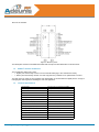
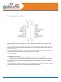
1.4. Hardware integration
TWIMO «RTU» (ready-to-use) module:
When integrating the TWIMO RTU
module, pins 13, 23, 26 & 27 MUST
BE CONNECTED TO THE GROUND.
If not done, the module won’t work.
Schematic on the left: typical hardware integration of the TWIMO RTU
module.
Note : the n/a pins are set in high
impedance state.
•
TWIMO «API» (programmable) module:
•
•
•
The Reset pin enables to reset
the module by applying a low
level Gnd signal.
The Boot pin enables to upgrade
the flash memory content.
When not used, this pin must be
connected to the ground via a
pull-down (47K) resistor.
The USART TX-RX-RTS-CTS
are TTL signals.
Free indicates that those pin can
be used as needed by the customer (please refer to «programmable» part of this manual).
1.5. Antenna
ADEUNIS RF will assist you in your choice of antennas so as to optimize the performance of your products. Feel
free to contact us for more information.
We suggest the schematic below:
TWIMO_Module_V1.4_user_guide
7
•
The footprint of the inductor and capacitor are useful to ensure good impedance matching between antenna
and TWIMO modules. The values will depend on the working RF frequency and characteristics of the
antenna.
•
The SMA connector can be bent or straight depending on the selected antenna but is not essential. We
could very well consider 8.6 cm welded wire antennas directly on the PCB either horizontally or vertically.
However and wherever possible, it is interesting to keep the footprint of SMAs as to facilitate the development for the degrees of freedom offered an application point of view (offset antenna, etc ...). We would offer
the antennas associated with these connectors.
•
For a quick set-up, we recommend not to get the self, to install the capacitor to 27 pF (or replace it by a
short circuit or a 0 ohm resistor) and solder a 8.6 cm length wire behind the capacitor.
1.6. Power Supply
The table below summarizes all the different electrical input/output generic characteristics of the modules.
Symbol
VIL
VIH
Parameter
Conditions
Input low level voltage
Std I/O input level
voltage
TTL ports
I/O FT input high level
voltage
VIL
Input low level voltage
VIH
Input high level voltage
Symbol
Parameter
VOL
Output Low level voltage for an I/O pin when
8 pins are sunk at the
same time
VOH
Output High level voltage for an I/O pin when
8 pins are sourced at
the same time
VOL
Output Low level voltage for an I/O pin when
8 pins are sunk at the
same time
VOH
Output High level voltage for an I/O pin when
8 pins are sourced at
the same time
VOL
Output Low level voltage for an I/O pin when
8 pins are sunk at the
same time
VOH
Output High level voltage for an I/O pin when
8 pins are sourced at
the same time
VOL
Output High level voltage for an I/O pin when
8 pins are sourced at
the same time
VOH
Output High level voltage for an I/O pin when
8 pins are sourced at
the same time
TWIMO_Module_V1.4_user_guide
CMOS ports
Conditions
Min
Typ
Max
-0.5
0.8
2
VDD+0.5
2
5.5
-0.5
0.35VDD
0.65VDD
VDD+0.5
Min
Max
Unit
V
V
Unit
0.4
TTL port
IIO=+8mA
2.7 V <VDD<3.6V
V
VDD-0.4
0.4
CMOS port
IIO=+8mA
2.7 V <VDD<3.6V
V
2.4
1.3
IIO=+20mA
2.7 V <VDD<3.6V
V
VDD-1.3
0.4
IIO=+6mA
2 V <VDD<2.7V
V
VDD-0.4
8
2.TWIMO concept
The idea behind TWIMO is to provide the user with a module which is ready for sending and receiving data over
a radio link thus enabling the user to focus on the development of its application. The aim is to relieve the user of
having to deal with the complex radio management.
TWIMO comes in two different versions:
• A “Ready To Use” version
• A “Programmable” version
Both versions use the same hardware base. The difference lies in the firmware which is running in the module.
However, from the user standpoint, both versions of the firmware provide an abstraction layer in charge of the
radio operating management.
2.1.
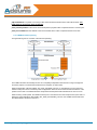
“Ready to Use” version: configurable RF gateway
The “Ready To Use” version is intended for user willing to embed a radio functionality onto their already existing
electronic design.
In the “Ready To Use” version the module operates in a standalone way and behaves like a
Serial <-> RF gateway. So in this case the user has to interface the module with a host processor where the
application code will be running.
Here is below represented the way it works: on the transmitter side the module will send data coming from the
serial link over the RF link and on the receiver side it will pass the data coming from the RF link to the serial link.
The communication is half-duplex.
Encapsulation
Figure 3.” Ready To Use” operating
2.2.
“Programmable” version: embedding your application in it!
The “Programmable” version is intended for user willing to embed their application onto the TWIMO module
itself. In this case the user is provided with an API library which purpose is to abstract the radio management. All
the user has to do is to focus on the development of its application code and invoke the API functions when the
application needs to send or receive data over the RF link.
3.“Ready To Use” version
3.1.
Operating modes
The “Ready To Use” version of the module may be operating in 2 different modes:
• The command mode
&
• The communication mode (default mode after reset)
TWIMO_Module_V1.4_user_guide
9
3.1.1 Command Mode
When the module is set to command mode the user is able to send command to the module in order to:
• Configure its parameters (radio parameters, serial parameters, communications parameters, etc.).
• Test its RF characteristics.
The chapter ¶3.2 describes all the commands which are available.
3.1.2 Communication mode
When the module is set to communication mode the user is able to exchange data with a remote module.
When in communication mode, there are basically 2 different “schemes” of communication: the communication
could be either asynchronous or synchronous.
3.1.2.01
Asynchronous mode of communication
The communication is said to be asynchronous when there is no coordination in the way the modules will access
the radio channel. So when a module is configured in asynchronous mode, the data coming on its serial interface
will be immediately sent over the radio link without any consideration regarding the radio channel occupancy. As
a consequence it is up to the user’s application protocol to manage the access to the radio channel in order to
avoid packets collision between equipments.
3.1.2.02
Synchronous (TDMA) mode of communication
The communication is said to be synchronous when there exists coordination in the way the modules will access
the radio channel. So when a module is configured in synchronous mode, the data coming on its serial interface
will be sent over the radio link at pre-defined instants, instants at which all the other equipment will be listening
(that is in radio reception mode).
One particularity of the synchronous mode is the presence of a Master equipment in the network. Its role is to
keep all the equipment involved in the network in sync: this is done by periodically sending synchronization frame
in order to re-adjust the timing of all equipment in the network.
When selecting this mode of communication the application does not have to deal (at all) with the radio channel
access => the module’s firmware is in charge of scheduling and coordinating the access to the radio channel and
thus making sure that no collision will never happen.
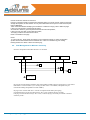
Here are described below the 2 main parameters that come into play when dealing with synchronous communication:
• The Number of slots: represents the number of equipment involved in the communication.
• The Slot Duration: represents the duration during which one of the equipment is transmitting data and all the
other equipment are listening (cf: ¶ 3.3.7 for detailled information).
Those 2 parameters are defined statically, which means that they cannot change dynamically during execution.
•
•
The Slot Number x Slot Duration gives the Cycle Duration.
The Cycle Duration must not exceed a maximum value above which the frequency deviation is such that
the equipments are not able to synchronize anymore. So the maximum number of slots in TDMA network is
limited to 50.
Find below the scheme of a synchronous network with 4 equipments:
TWIMO_Module_V1.4_user_guide
10
Figure 6. TDMA network with 4 equipments
3.1.2.03
Synchronous vs Asynchronous (drawback and advantage)
The main advantage of the synchronous mode over the asynchronous mode is that the user does not have to
worry about the radio channel access instant and thus does not have to worry about RF collision.
However the synchronous mode may suffer from poor response time as well as decreased data rate compare to
asynchronous mode. Indeed as the number of equipment in a synchronous network will increased, the data rate
will decrease and the response time will increase.
For instance the synchronous mode will be useful in application where a user wants several independent systems to coexist.
As an example let us take status reporter application where 2 sets of equipment have to operate within the
same geographic area. Selecting asynchronous mode will require the 2 sets of equipment to communicate on 2
different frequency channels (with a channel spacing large enough in order to avoid interference). In some cases
this requirement might not be achievable. So the only solution is to go for a synchronous mode of communication
where several set of independent equipment will be able to communicate without interfering each other.
So the decision to go for one mode or another is very dependent on the application’s requirements: data rate
expected, response time needed, deployment scheme, 1/2-way communication etc...
3.2.
Command Interface
The command interface consists of a set of command enabling the user to configure the radio module and run
test on the radio module.
3.2.1 Entering Command Mode
Entering the command mode can be achieved in 2 different ways:
3.2.1.01
Through the RS232 serial link
Using a specific sequence of ASCII character: only upon reset with the serial link speed fixed to 9600 bauds and
flow control disabled. The sequence of character to use is the following:
-> Hold the «!» key pressed and reset the module.
-> Wait for the module to send the “O” character
-> Send the “K” character to the module
-> The module will send the message “CMD_MODE_ON” when entering the command mode.
TWIMO_Module_V1.4_user_guide
11
ATEX (see fig.7) command does not enable to switch to communication mode. The user must reset the module.
3.2.1.02
Through a dedicated pin of the module (pin n° 8: Cmd_Mode):
-> Upon reset using a level detection (the level must be held for at least 500ms): in this case the serial link
speed is fixed to 9600 bauds and flow control is disabled.
or
-> During execution using rising edge detection: in this case the serial link speed and flow control type are set
with user’s setting.
ATEX (see fig.7) command, allows you to quit the command mode ONLY if «During execution» procedure
has been chosen to enter command mode. If not chosen, the user must reset the module.
3.2.2 AT Commands
A command starts with the 2 ASCII characters “A” + “T” and ends with the 2 characters “CR” + “LF”.
A response is sent back to the user after each command.
The «command» can be divided in 2 groups:
3.2.2.01
AT Commands : module configuration
The first group contains commands which are mainly used to read and update the modem parameters:
Commands
Descriptions
Responses
ATSn?
Returns the content of the Sn register
Sn=y<cr><If>, y is the content of the Sn rgister
ATSn=m
Set the content of the Sn register with the value m
The register content is updated in volatile memory
«O»<cr> if operation OK, «E»<cr> if error
AT/S
Display as a list, the content of each register
Sxxx=y<cr><lf> for each register
AT/V
Displays the firmware version
TW_AA_Vx.x.xx_AA_A_x.xx
ATR
Restore the content of registers (in non-volatile
memory) with default values.
«O»<cr> if operation OK, «E»<cr> if error
ATEX
Exit command mode
«O»<cr> if operation OK, «E»<cr> if error
AT&W
Save the register configuration in non-volatile
memory
«O»<cr> if operation OK, «E»<cr> if error
Figure 7. AT Command configuration
3.2.2.02
AT Commands : module test
The second group contains commands which are used to run RF test on the module:
Commands
Descriptions
Responses
ATT11
Configure the radio in continuous reception mode
«O»<cr> if operation OK, "E"<cr> if error
ATT12
Reset the packet counter
«O»<cr> if operation OK, «E»<cr> if error
ATT13
Return the number of correctly received packet (and
configure the radio in Standby mode)
«O»<cr> if operation OK, «E»<cr> if error
ATT21
Pure carrier (data=0) transmission using current RF
channel
«O»<cr> if operation OK, "E"<cr> if error
ATT22
Pure carrier (data=1) transmission using current RF
channel
«O<cr> if operation OK, «E»<cr> if error
ATT23
0x55 modulated carrier using the current data rate
and RF channel
«O»<cr> if operation OK, «E»<cr> if error
ATT24xx
Burst packet mode. Send xx data packet (15 bytes)
consecutively with 100 ms spacing between 2
packets.
«O»<cr> if operation OK, «E»<cr> if error
NB 1: ATT21 to ATT24 commands are only dedicated to test purposes. The end product can’t be used in this conditions
NB 2: the test commands are available only if the module is configured is asynchronous mode.
TWIMO_Module_V1.4_user_guide
12
3.2.3 Register parameter
All the user settings are contained in registers located in E2PROM memory.
At power up, the previous configuration is loaded from E2PROM to RAM memory. Then every register update
(using the ATSn=m) will modify the register content in RAM memory. In order to save the current configuration in
non-volatile memory (E2PROM) the user has to use the command AT&W.
List of registers with their descriptions:
Register
Type
Default
Note
Effect
0
Correspond to the gross data rate
Immediate
201
RS232 baudrate
0: 9600 bauds
1: 38400 bauds
2: 57600 bauds
0
The other RS232 parameters are fixed:
- 1 stop bit
- No parity
- 8 bit of data
At next reset
202
RS232 hw flow control
0: disable
1: Enable
0
Only RTS signal is managed in order to
inform the host to stop sending data
At next reset
203
RS232 condition for packet transmission
0: MaxPackSize Only
1: MaxPacketSize or RS232 Timeout
1
RS232 timeout si timeout for silence detection. This timeout is fixed to 100ms.
At next reset
204
Adressing mode
0: Transparent
1: Adressed
0
205
N/A
206
MAC
0: ASYNC
1: TDMA
0
Select the medium access scheme
At next reset
207
Device Role
0: Master
1: Slave
1
Applies only if register 206=1
At next reset
Radio Data Rate
0: Narrow Band (10 kbps)
1: Medium band (38,4 kbps)
2: Wide Band (57,6 kbps)
200
Immediate
208
209
210
N/A
211
212
213
Radio channel for communication (MHz)
868
214
0: N.A
1: N.A
2: 868,120
3: 868,170
4: 868,220
5: 868,270
6: 868,320
7: 868,370
8: 868,420
9: 868,470
10: 869,500
11: 869,525
12: 869,550
433
915
11
N.A
Immediate
N.A
Figure 9. Register description
TWIMO_Module_V1.4_user_guide
13
Register
Type
RF output power (dBm)
LP
MP
HP
215
0: 10
1: 14
2: 17
N.A
0: 20
1: 23
2: 27
Default
Note
Effect
2
Immediate
At next reset
216
Op Freq
0: 868MHz
1: 434MHz
2: 915Mhz
0
217
Source Address (=local device @)
from 1 to 254
default value: 1
218
Applies only if register 204=1
Value 0 is reserved for master device in
TDMA mode
Immediate
TDMA device slot offset
from 1 to 49
Applies only if register 206=1
Value 0 is reserved for master device
At next reset
219
Number of slots inTDMA network
from 2 to 50
Applies only if register 206=1
At next reset
220
Destination Address (=remote device @)
from 0 to 255
Applies only if register 204=1
225 is Broadcast @
Immediate
Scrambling the user data before radio
transmission so to prevent DC bias in the
transmitted signal.
No
For test purposes only !
If the voltage goes below 2.6V an
onboard LED will light and the radio will
stop working. The user must reset the
module.
No
default value: 255
221
N/A
222
DC Free
0: Disable
1: Enable
223
224
1
Low Bat detect Level
3.2.4 Default settings
By default the USART is configured at 9600 baud with no flow control enabled, 8 bit data, 1 stop bit and no parity.
The default radio settings are: narrow band (10 kbps) on frequency channel 869.525 MHz with an output power
set to the maximum value (that is 27dBm for HP module and 17dBm for MP module).
The default medium access scheme is asynchronous in transparent mode.
3.3.
Communication mode: Sending and Receiving datas
The communication is always half-duplex.
By default the radio is in reception mode waiting for an incoming packet. It goes to transmission mode when
datas have to be sent.
Whatever the medium access scheme (whether it is asynchronous or synchronous) the transmission of a radio
packet starts as soon as one of the 2 following conditions is met:
TWIMO_Module_V1.4_user_guide
14
•
•
The number of character received from the serial link is equal to the maximum packet size (i.e 60 bytes).
A silence greater then 100ms has been detected on the serial link since the reception of the last character.
3.3.1 Modem state machine
The internal system architecture is made up of 2 software tasks:
• 1 task dedicated to the management of the Transmission path (i.e. path going from the serial link to the
radio link).
and
• 1 task dedicated to the management of the Reception path (i.e. path going from the radio link to the serial
link).
Both tasks make use of different FIFO buffer. As a consequence the Transmission and Reception path are
completely independent. Basically it means that data coming from the serial link will be accepted even if a radio
frame is being demodulated.
Both the transmission and reception FIFO contains 4 buffers. Waiting for the radio engine to be available for
transmission, the system will be able to buffer up to 4 consecutives data frame coming from the serial link.
So by default the system is waiting for incoming data on the serial link and waiting for incoming data on the radio
link.
On the serial link side, as soon as one of the two conditions (mentionned before - see ¶3.3) is met, a radio packet is built up and put into the transmission FIFO buffer. Then the packet will be sent over the air as soon as the
radio engine becomes available for transmission.
3.3.2 Data flow
Radio data rate and serial data rate must be carefully chosen in order to avoid losing data.
If the radio data rate is higher than the serial data rate:
The bottleneck will occur on the receiver side:
On the radio transmitter side, an inter-frame time must be respected in order to avoid overrun on receiver side.
If the radio data rate is lower than the serial data rate:
The bottleneck will occur on the transmitter side:
The radio transmitter will not be able to send data fast enough to release the buffer for new data.
To solve this problem, the serial hardware flow control must be used. So the host connected to the transmitter
equipment will wait for the buffer to become free before sending new data.
3.3.3 Packet format
Find below a description of the TWIMO packet format:
TWIMO_Module_V1.4_user_guide
15
The Preamble duration depends on the radio data rate selected through the register 200:
• For narrow band communication (i.e. 10 kbps), the preamble duration is 20 ms that is 25 bytes length.
• For medium band communication (i.e. 38.4 kbps), the preamble duration is 6.5 ms that is 32 bytes length.
• For wide band communication (i.e. 57.6 kbps), the preamble duration is 5 ms that is 36 bytes length.
The purpose of the preamble is to enable the receiver to set up the AFC and AGC blocks so to correctly received
the subsequent data.
The Synchronization field is 4 bytes length.
After the Synchronization bytes, the packet contains a 4 bytes “packet header”:
The Length field is 1 byte length and contains the length of the Payload plus 1 or 3 bytes (depending on the
Addressing mode settings) to account for the Type byte and the Source and Destination address bytes.
The Source and Destination address bytes are there only if the register 204 is set to 1 (that is Addressed mode
selected). The Source is the address of the “local” equipment. The Destination field indicates the address of the
remote device to whom the packet is intended for.
Nb : in synchronous mode, the source byte is always present even if addressing mode is set to «transparent».
So in transmission the Source field contains the transmitter address and the Destination field contains the remote
device address.
So on the receiver side, the Destination field is compared with the receiver’s Source address to decide whether
the packet should be accepted or rejected.
The Type field (1 byte) indicates the type of the packet. A packet could be of different type: Data packet, Control
packet etc…This field is handled internally by the modem’s firmware. The user does not have to worry about this
field.
The Payload contains the data message to transmit from one equipment to another. The size of the payload is in
the range [1 -> 60] bytes.
The CRC checksum is a 2 bytes field which enables the receiver to perform error detection.
3.3.4 Addressing modes
3.3.4.01
Transparent mode
When “Transparent” mode is set:
On the transmitter side, the data are sent without any specific destination address. So it is up to the user’s application to encapsulate the destination address in the payload of the packet.
TWIMO_Module_V1.4_user_guide
16
On the receiver side, it is up to the user’s application to strip off the encapsulated destination address from the
received data stream.
3.3.4.02
Addressed mode
When “Adressed” mode is set:
On the transmitter side, the data are sent with a specific destination address (the value contained in the register
204). Broadcast packet can be sent by using the destination address 255.
On the receiver side, only the packets whom the destinations address match the local equipment address will be
processed. The other will be discarded.
3.3.5 Receiving mode
In reception, the TWIMO RF engine employs a preamble-detection based mechanism, which garantees optimal
performances in sensitivity.
3.3.6 LED Status
The TWIMO module is equipped with an onboard LED.
• LED blinks : following packet reception or packet transmission.
• LED lights : voltage goes below the «low batt detect» threshold.
3.3.7 Synchronous TDMA mode
The slot duration is fixed and set to the time it would take to send over the radio a packet with the maximum size,
that is 60 bytes.
•
So for Narrow band communication, the slot duration is equal to:
=> 70 ms.
•
For Medium band communication, the slot duration is equal to:
=> 20 ms.
•
So for Wide band communication, the slot duration is equal to:
=> 15 ms.
As said in previous chapter (cf. 3.1.2.2), the cycle duration is equal to the slot duration multiply by the number of
slot. However to be compliant with the authorities certification, the radio system must respect certain duty cycle
in terms of transmit duration.
For instance on the 869.525 MHz channel, the duty cycle is 10%, which means that any single equipment should
not transmit for more than 10% of the time.
As a consequence for a TDMA network with less than 10 equipments, the cycle duration is equal to the slot
duration multiply by 10.
Then for a TDMA network with 10 or more equipment, the cycle duration is equal to the slot duration multiply by
the actual number of slot.
This adjustment is automatically carried out by the module’s embedded firmware.
TWIMO_Module_V1.4_user_guide
17
3.4.
Radio characteristics
3.4.1 Narrow band system
Narrow band operating characteristics:
Module
Data Rate (kbps)
Channel available
Sensitivity (dBm)
Preamble (ms)
10
3
-110
20
Channel available
Sensitivity (dBm)
Preamble (ms)
-106
6.5
High Power
Medium Power
3.4.2 Medium band system
Medium band operating characteristics:
Module
Data Rate (kbps)
High Power
1
38.4
Medium Power
9
3.4.3 Wide band system
Wide band operating characteristics:
Module
Data Rate (kbps)
Channel available
Sensitivity (dBm)
Preamble (ms)
57.6
1
-102
5
High Power
Medium Power
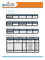
3.4.4 Summary
The table below summarizes the {frequency channel, output power, data rate} combination allowed according to
the normative requirements:
TWIMO module
ARF7581 (HP868)
ARF7580 (MP868)
RF Data Rate
Authorized frequencies
RF Power
Authorized frequencies
RF Power
Narrow Band
10kbps
869.500 MHz
869.525 MHz
869.550 MHz
27dBm
27dBm
27dBm
869.500 MHz
869.525 MHz
869.550 MHz
17dBm
17dBm
17dBm
Middle Band
38.4kbps
869.525 MHz
27dBm
869.525 MHz
868.120 MHz
868.170 MHz
868.220 MHz
868.270 MHz
868.320 MHz
868.370 MHz
868.420 MHz
868.470 MHz
17dBm
14dBm
14dBm
14dBm
14dBm
14dBm
14dBm
14dBm
14dBm
Wide Band #1
57.6kbps
869.525 MHz
27dBm
869.525 MHz
17dBm
TWIMO_Module_V1.4_user_guide
18
4.Firmware upgrade
Firmware upgrade is possible through the UART (only Tx and Rx are required) communication link.
The Boot signal must be maintained to Vcc (3.3v) while resetting the module (that is low level on Reset pin for
500 ms).
The module enters a bootloading mode which enables the user to proceed with a firmware upgrade.
The STM32 flash loader application must be used on the PC side to download the binary. The STM32 flash
loader application can be executed from a user friendly graphical interface but also from the Windows command
line (more information and download can be found on Adeunis RF website www.adeunis-rf.com).
TWIMO_Module_V1.4_user_guide
19
5.“Programmable” version
The “Programmable” version is intended for user willing to embed their application onto the TWIMO module
itself.
In order to abstract the radio management, Adeunis-RF provides the user with an API library containing a set of
functions used to send and receive data without having to worry about all the complexity involved in the radio
operating management.
In other words, all the user has to do is to focus on the development of its application code and invoke the API
functions when the application needs to send or receive data over the RF link.
5.1.
API concept
The TWIMO concept consists in:
• Enabling the user to develop and embed its application onto the module’s microcontroller.
• Providing the user with an Application Programming Interface in charge of abstracting the radio operating.
So it becomes easy for anyone with programming skills (but no radio skills at all) to come up with a wireless
enabled product.
As described further, a TWIMO module has got a very rich hardware interface that makes it possible for the user
to interface a TWIMO module with a lot of different external hardware peripherals.
TWIMO_Module_V1.4_user_guide
20
5.2.
Hardware Interface description
5.2.1 Pin Description
Pin
module
6
8
10
11
12
13
14
15
16
17
21
22
23
24
25
26
27
29
I/O µC
Default config*
Interrupt capability
Alternate Config 1
Alternate Config 2
Alternate Config 3
PA0
PB1
PA9
PB14
PA10
PB13
PA12
PB15
PA11
PB12
PA4
PA5
PA1
PB10
PB11
PA2
PA3
PA8
GPIO
GPIO
GPIO
GPIO
GPIO
GPIO
GPIO
GPIO
GPIO
GPIO
GPIO
GPIO
GPIO
GPIO
GPIO
GPIO
GPIO
GPIO
Yes (WakeUp)
Yes
No
No
No
No
No
No
No
No
Yes
No
Yes
No
No
Yes
Yes
No
ADC_0
ADC_9
USART1_TX
SPI_MISO
USART1_RX
SPI_SCK
USART1_RTS
SPI_MOSI
USART1_CTS
SPI_NSS
ADC_4
ADC_5
ADC_1
TIMER
TIMER
ADC_2
ADC_3
MCO
USART2_CTS
TIMER
TIMER
USART3_RTS
USART3_CTS
USART3_CK
USART2_CK
USART2_RTS
USART3_TX
USART3_RX
USART2_TX
USART2_RX
USART1_CK
TIMER
I2C_SCL
I2C_SDA
* the GPIOs are configured as floating inputs
•
•
•
•
•
The pin 6,8,23,24 & 25 can be configured as timer input or output (Input Capture, Output Compare, PWM).
Pin 6 can be used to wake up the µC from sleep mode.
Pin 3 is the Antenna pin. Special care should be taken when designing the antenna in order to obtain an
optimal matching.
Pin 7 is the Reset pin. This pin is used to reset the module. Reset occurs when this pin is put to low for at
least 500 ms.
Pin 9 is the Boot pin. This pin is used to set the module in bootload mode. This mode can be used to
upgrade the flash content.
5.3.
Resources availability and partitioning
The hardware resources available must be shared between the TWIMO API code and the user application code.
The TWIMO API code being in charge of the radio management, a lot of resources are required.
5.3.1 Flash memory
The module’s microcontroller has got 64 Kbytes of flash memory.
This memory is used to:
• Store and execute code
• Store constant variable
5.3.2 RAM memory
The module’s microcontroller has got 10 Kbytes of RAM memory.
This memory is used to:
• Store local variables.
• Store a copy of the global variables used in TWIMO API code: the purpose is to speed up the API code
execution.
TWIMO_Module_V1.4_user_guide
21
•
Store the stack and heap: API code requires a certain amount of stack (default value in .icf file). Then it is up
to the user to increase this size if required.
5.3.3 E2PROM memory
•
The µC does not contain E2PROM memory. So flash memory must be used to emulate E2PROM (E2PROM
memory driver are not provided by Adeunis RF).
5.3.4 TWIMO firmware requirement in terms of memory
The TWIMO API library (Radio API) occupies about 20 KBytes of flash memory and requires about 3 Kbytes of
RAM memory (this does not take into account the stack space needed!).
In spite of the fact that the TWIMO API code requires only 20 Kbytes of flash, only 16 Kbytes of flash memory are
left for the user to put its application code.
5.3.5 Peripheral (GPIO, ADC/DAC, Communication etc…)
Available peripherals :
• Up to 3 USARTs can be used simultaneously.
• Another possible configuration is 1 USART, 1 I2C and 1 SPI simultaneously.
All pin can also behave like GPIO. When configured as GPIO, only pin 6.8.21.23.26 & 27 will have interupt capability.
As of now Adeunis-RF doesn’t provide any peripheral’s driver. However ST provides a peripheral’s library which
enables the user to quickly get started with using the peripherals. Please contact us for any additional details.
For any information related to the peripheral implementation, the user must report to the microcontroller User
Manual.
5.3.6 Hardware Timer
Three 16-bit timers are available, each one with 4 Output Compare/Input Capture/PWM counter: TIM2/3/4.
One 24-bit systick timer is also available.
Two of the three 16-bit timers are dedicated to the radio management: TIM3 and TIM2.
So only the TIM4 remains available for the user.
The 24-bit systick timer is used by the TWIMO API code as a free running timer in order to provide a 1 ms time
base.
5.3.7 DMA
TWIMO_Module_V1.4_user_guide
22
The microcontroller embeds a 7-channel DMA controller.
Here is below the different channel with their possible usage (extracted from STM32 User Manual):
Channels 2, 3, 6 and 7 are not available to the user application code since they are dedicated to the radio driver
operating
So only DMA channels 1, 4 and 5 remain available for the user application code.
5.3.8 GPIO Interrupt line and vectors
The interrupt vectors associated with peripherals (that are free for the application) are available for use by the
application code.
However the interrupt vector associated with the GPIO (that are free for the application) are not all available to
the application code.
Indeed some of the GPIO interrupt lines are multiplexed on a single interrupt line: this is the case for interrupt
lines 5, 6, 7, 8 and 9 as well as for interrupt lines 10, 11, 12, 13, 14 and 15.
It happens that interrupt line 6, 7, 8, 9 and 13 are dedicated to the radio driver operating.
As a consequence the interrupt vector corresponding to the interrupt line onto which line 6, 7, 8 and 9 are multiplexed is not available to the application code. The same applies for the interrupt vector corresponding to the
hardware interrupt line onto which line 10, 11, 12, 13, 14 and 15 are multiplexed.
The reason why this access is not given is because it may jeopardizes the radio operating.
So this is below the GPIO lines for which an interrupt vector is available to the application code:
NB: It is important to note the following: pin 8 and pin 23 of the module cannot be simultaneously connected to
the interrupt line number 1.
5.3.9 Interrupt vector priority
TWIMO_Module_V1.4_user_guide
23
It is important to grant high priority to interrupt vector involved in the radio driver operating.
So this is below the list of available interrupt vectors as well as the priorities assigned to each of them:
The interrupt vectors involved in the TWIMO firmware have a fixed and higher priority than the interrupt vectors reserved for the application code. The purpose is to make it possible for TWIMO’s interrupt vectors to preempt
the Application’s interrupt vector if needed.
By default the priority of the application’s interrupt vectors are set to 2 and the sub-priority is set to 0. If needed
the user may also use a level 3 of priority and level 1, 2 or 3 for the sub-priority.
The sub-priority is there to determine the order of execution in case there are multiple pending interrupt with the
same priority level.
5.3.10
CPU Frequency
The CPU frequency is set to about 16 MHz (15.75 MHz exactly). As of now only one frequency operating is available. In the future Adeunis RF will be offering other CPU frequencies in order to better fit the application requirement: for instance a 2 or 4 MHz CPU frequency for battery powered application, a 24 or 32 MHz CPU frequency
for application with “hard” real time constraints.
Then user should not attempt to change the CPU frequency by himself since the radio related timing are
computed considering a 16MHz CPU clock.
5.4.
API TWIMO
TWIMO_Module_V1.4_user_guide
24
This chapter presents all the TWIMO API functions: parameter(s), return value and description.
This chapter also describes all the data structures that the user has to manipulate in order to use the API functions.
5.4.1 Radio related APIs
5.4.1.01
TWIMO_API_SystemInit()
i)Prototype
Here is the function prototype:
TWIMO_ERROR_CODE TWIMO_API_SystemInit (struct TWIMO_INIT *);
This function takes 1 parameter:
•
A pointer to an instance of the TWIMO_INIT structure (cf. chapter 1.5.4 for the definition of this structure).
This function returns TWIMO_OK if everything went OK and TWIMO_NOK_4 if something went wrong with the
initialization.
ii)Description
This function is in charge of carrying out all the hardware and software initializations required for the TWIMO
firmware to work.
This function configures:
• The system clock
• The radio register
• The µC hardware peripherals: SPI_1, DMA1_CH2/3/6/7, TIM2/3, SysTick timer, GPIO configuration, Interrupt….
• The memory buffering system
• The software contexts
• Etc...
This function must be invoked at the beginning of the application program (cf. Adeunis Application example).
5.4.1.02
TWIMO_API_Radio_BackgroundTask()
i)Prototype
Here is the function prototype:
void
TWIMO_API_Radio_BackgroundTask (struct TWIMO_INIT * );
This function takes 1 parameter:
• A pointer to an instance of TWIMO_INIT structure (cf. chapter 1.5.4 for the definition of this structure).
This function does not return anything.
ii)Description
This function must be regularly invoked in background by the application code (cf. chapter 5.6 Integration).
TWIMO_Module_V1.4_user_guide
25
This function is the main part of the radio driver.
5.4.1.03
TWIMO_API_Radio_SendData ()
i)Prototype
Here is the function prototype:
TWIMO_ERROR_CODE TWIMO_API_Radio_SendData ( struct TWIMO_INIT *, struct TWIMO_RADIO_TX * );
This function takes 2 parameters:
• A pointer to an instance of the TWIMO_INIT structure (cf. chapter 1.5.4 for the definition of this structure).
• A pointer to an instance of the TWIMO_RADIO_TX structure (cf. chapter 1.5.4 for the definition of this structure).
The TWIMO _RADIO_TX structure basically contained 3 fields:
• Input parameter: A pointer to the “source” buffer that is the buffer containing the data to be sent over the
radio.
• Input parameter: The size (in bytes) of the data buffer. The size must be comprised between 1 and 60 bytes
maximum.
• Input parameter: The Destination address (address of the remote receiver device to whom the data are
intended to): value between 0x00 and 0xFF. This field is ignored by the API function if Transparent mode is
selected. 0xFF is a broadcast address!
From the API function point of view those 3 fields are input parameters.
This function returns TWIMO_OK if the data has been accepted and TWIMO_NOK_1 if the data cannot be
accepted (because the transmit FIFO is full).
If TWIMO_OK is returned the application code can release its «source» buffer.
ii)Description
This function is in charge of inserting the data buffer onto the transmission FIFO (which can contain up to 4
buffers).
The data will then be sent over the air as soon as the radio engine will be available for it.
5.4.1.04
TWIMO_API_Radio_ReceiveData()
i)Prototype
Here is the function prototype:
TWIMO_ERROR_CODE TWIMO_API_Radio_ReceiveData ( struct TWIMO_INIT *, struct TWIMO_RADIO_RX * );
This function takes 2 parameters:
•
•
A pointer to an instance of the TWIMO_INIT structure (cf. chapter 5.4.3 for the definition of this structure).
A pointer to an instance of the TWIMO_RADIO_RX structure (cf. chapter 5.4.3 for the definition of this structure).
The TWIMO_RADIO_RX structure basically contained 3 fields:
•
Input parameter: A pointer to the “destination” buffer that is the buffer onto which the received data will be
TWIMO_Module_V1.4_user_guide
26
•
•
stored.
Caution: as the application does not know in advance what the received packet’s size will be, it must allocate room for the maximum size, which is 60 bytes
Output parameter: The size (in bytes) of the received packet’s payload. The size is comprised between 1
and 60 bytes.
Output parameter: The Source address of the received packet (address of the remote sender device): value
between 0x00 and 0xFE.
From the API function point of view the first field is an input parameter and the two last fields are output parameters.
This function returns TWIMO_NOK_2 when no data have been received (that is the reception FIFO is empty);
else the function returns TWIMO_OK.
ii)Description
This function is in charge of extracting a data buffer from the reception FIFO (which can contain up to 4 buffers)
and copy the data onto the buffer passed in parameter.
This function must be called on a regular basis in order to make sure that no overflow occurs at the reception
FIFO level. In case of overflow, there is a risk of packet loss.
If Addressed mode is selected (cf. chapter 5.4.3 TWIMO_INIT structure definition), the TWIMO firmware will
automatically filter out received packet whom destination address does not match the local device address. If
there is a match then the received packet will be put into the reception FIFO.
If Transparent mode is selected (cf. chapter 5.4.3 TWIMO_INIT structure definition), the TWIMO firmware will put
every received packet into the reception FIFO.
5.4.1.05
TWIMO_API_GetFirmwareVersion()
i)Prototype
Here is the function prototype:
void
TWIMO_API_GetFirmwareVersion (uint8_t * );
This function takes 1 parameter:
-
A pointer to a string of character. The string of character must be at least 23 character.
This function does not return anything.
ii)Description
This function returns the firmware version.
5.4.2 TWIMO API data structure
5.4.2.01
TWIMO_INIT
TWIMO_INIT is a typedef structure containing the user settable parameters. Here is below the structure definition:
TWIMO_Module_V1.4_user_guide
27
Radio_FreqChannel enables the user to select the frequency communication channel. Around 70 frequency
channels (between 863 Mhz and 870 MHz) are available to the user.
Radio_DataRate enables the user to select the air data rate. There are 3 possible values: 10 kbps, 38.4 kbps
and 57.6 kbps.
Radio_OutputPower enables the user to select the radiated RF power. There are 3 possible values (which are
different depending on the Radio_ModuleType setting): 10 dBM, 14 dBm and 17 dbm for Medium Power module
and 20 dBM, 23 dBm and 27 dbm for High Power module.
Radio_MediumAccess enables the user to select the medium access scheme. As explained in the TWIMO
User Guide, there exist 2 possible schemes: Asynchronous or Synchronous (also referred as TDMA).
Radio_AdressingMode enables the user to select the addressing mode. As explained in the TWIMO User
Guide, there exist 2 possibilities: Transparent or Addressed.
Radio_DeviceAddress enables the user to select an address (value between 0x00 and 0xFE) for the local
device. In Synchronous mode (TDMA) this field is used to allocate a slot position in the TDMA cycle: the value
0x00 is reserved for the Master device.
In transmission, this address will always appear as the “source” address in the packet header (refer to TWIMO
User Guide). In reception, this address will be compared with the receive packet’s destination address to decide
on the packet acceptance.
Radio_ModuleType enables the user to select the type of radio module he is working on. There are 2 possibilities: MP (Medium Power) or HP (High Power).
Radio_DeviceRole enables the user to select the role of the local device when Synchronous (TDMA) mode is
selected. There are 2 possibilities: Master or Slave. Please refer to the TWIMO User Guide for more information
about TDMA mode.
Radio_TdmaNetworkSlotNum enables the user to select the total number of slot which corresponds to the total
number of devices involved in the TDMA network (including the Master device). The minimum value is 0x02 and
the maximum value is 50.
Radio_TdmaSlotOffset enables the user to select the slot offset for the local device. The slot offset (in relative
TWIMO_Module_V1.4_user_guide
28
to the Master slot that is equal to 0x00) gives the slot into which the device will transmit its data. The value 0x00
is reserved for the Master device. So the possible values for a Slave device are: 0x01 -> 0xFF. total number of
devices involved in the TDMA network (including the Master device).
Twimo_Context_Ptr is a pointer to an instance of the TWIMO_CONTEXT structure. This structure contains
pointer to the context of all the block of the TWIMO firmware. The user needs to declare an instance of this structure (cf. example of Application based on TWIMO API).
It is kindly recommended to refer to Adeunis-RF for the choice of the { Radio_FreqChannel, Radio_DataRate,
Radio_OutputPower } combination. Indeed this choice must match the RTTE recommendations…
TWIMO_RADIO_CHANNEL, TWIMO_RADIO_DATARATE, TWIMO_RADIO_OUTPOWER, TWIMO_RADIO_
MAC, TWIMO_RADIO_ADDRESSING, TWIMO_RADIO_MODULE and TWIMO_RADIO_ROLE are typedef
ENUM defined in the api_twimo.h interface file.
5.4.2.02
TWIMO_RADIO_TX
TWIMO_RADIO_TX is a typedef structure containing the user settable parameters. Here is below the structure
definition:
[[IN] DataBufferPtr is a pointer to the memory buffer containing the data to send over the air.
[IN] DataBufferSize is the data buffer size. Value comprises between 1 and 60 bytes.
[IN] DestinationAddress is the address of the remote receiver device. Value comprises between 0 and 255.
This field is ignored if in Transparent mode.
NB: The value 255 corresponds to a broadcast address.
5.4.2.03
TWIMO_RADIO_RX
TWIMO_RADIO_RX is a typedef structure containing the user settable parameters. Here is below the structure
definition:
TWIMO_Module_V1.4_user_guide
29
[IN] DataBufferPtr is a pointer to a memory buffer where the data received from the radio will be stored. This
buffer must be of size max, which is 60 bytes.
[OUT] DataPayloadSize is the size of the received packet’s payload. Value comprises between 1 and 60 bytes.
[OUT] SourceAddress is the address of the remote sender device. Value comprises between 0 and 254.
5.4.3 TWIMO firmware operating
The figure below gives an overview of the firmware operating.
The TWIMO firmware can basically be seen as a completely independant task which is running in background
and which purpose is to handle the transmission and reception of radio frames.
When the application calls the TWIMO_API_Radio_SendData () function, a new element is put onto the transmission FIFO (FIFO size is 4 elements). Then the application does not have to deal with the transmission of the
packet over the radio. The TWIMO firmware will proceed with the packet radio transmission as soon as it can.
When receiving a radio packet, the TWIMO firmware puts a new element onto the reception FIFO (FIFO size is 4
elements). When application calls TWIMO_API_Radio_ReceiveData () function, the TWIMO firmware will return
the oldest element contained in the FIFO.
TWIMO_Module_V1.4_user_guide
30
5.4.4 Application Template
5.5. TWIMO API: how to use it ?
Adeunis RF is providing the customer with a demonstration package containing the following elements:
•
A .c file, app_main.c, containing an application template, i.e. the main() function and all the global variables
needed for the TWIMO API code to execute properly. The purpose of this application is to demonstrate how
to make use of the TWIMOP API to send and receive data over the radio link.
•
A .c file, app_it.c, containing most of the interrupt vectors available for the user application.
•
A .h file, api_twimo.h, containing the TWIMO API’s global structures definition, the #define constant needed
and the TWIMO API function prototypes.
•
An .icf file containing the memory section and placement information. The user must include this file into its
development workspace (IAR). The Stack and Heap size may be changed in this file. However it is recommended to the user not to change the other parameters.
•
A startup file in charge of all the initialization.
TWIMO_Module_V1.4_user_guide
31
•
An IAR development tool workspace template with correct option settings.
•
The STM32 peripherals driver library.
•
The TWIMO API firmware, which is provided as a library of functions (.a file).
The purpose of this “demonstration package” is to help the user to quickly get started with the TWIMO API functions and all the aspects pertaining to the code generation tool environment.
NB: by default all modules delivered by Adeunis-RF to customer contains the “Ready To Use” Adeunis-RF application in it. On top of that the µC access is locked for security reason. So it is up to the user to unlock the flash
memory in order to be able to flash it again or to be able to debug its application. For this the user must run the
STM flash loader.
5.6. Code Integration
Here are the constraints that have to be taken into account when integrating application code with the TWIMO
API firmware:
5.6.1 Application background task execution
It is important for the user to make sure that the application firmware does not prevent the TWIMO firmware from
properly operating (to prevent packet loss from happening): this means that the application background task
should be as short as possible in order to let the TWIMO background task to execute on a regular basis.
The latency allowed between 2 consecutives call to this function mainly depends on 2 parameters:
-
The radio data rate which is employed
-
The inter-frame duration employed.
The higher the data rate the lower is the allowed latency.
By the same token, the lower the inter-frame duration the lower is the allowed latency.
So as a general rules, it is recommended to cut out as much as possible the background processing.
To give an order of magnitude:
If there is no constraint on the inter-frame duration, then the max latency allowed will be about 10ms (NB), 3 ms
(MB) and 2 ms (WB).
In case there is harsh constraint on the inter-frame duration (for instance back to back packet), then the max
latency allowed might fall down to 3 ms (NB), 0.8 ms (MB) and 0.5 ms (WB).
5.6.2 Application interrupt execution
By the same token, it is very important for the user to make sure that the execution of the interrupt handlers is as
short as possible in order to avoid jeopardizing the radio driver operating.
5.6.3 Miscellaneous
The user must respect all the integration rules regarding the peripheral available, the interrupt priority and so on.
5.7. Compiling code
5.7.1 Code Generation tool
As of now, the only tool compatible with the TWIMO firmware is the IAR development tool for ARM.
A licence-free version (KickStart version 5.41) is available and might be downloaded from Adeunis web site.
However this version is limited to 32 Kbytes of compiled code.
TWIMO_Module_V1.4_user_guide
32
Then the user must switch to a licensed version with a 256 Kbytes limitation.
5.7.2 Project/Workspace exemple
Like mentioned previously, Adeunis RF is providing a template of the workspace with the correct option to select
in order to be compatible with the TWIMO API firmware.
5.8. Bootloading
The bootloading will enable the user to upgrade the firmware. As of now only serial (through USART, TX and Rx
only) bootload is possible.
To enter bootloader mode, the BOOT pin (number 9) must be held to high and then the RESET pin (number 9)
must be pulled down for at least 500 ms.
6.Process
6.1. Description of module 7581-A and board ARF7628/B
7581 module is fully SMT, single side. Assembly process is based on leadfree alloy, no clean flux residues
Main component families are:
- Ceramic chip resistors and capacitors,0201size (0.5 mm x 0.25 mm)
- Ceramic chip resistors and capacitors, 0402 (1 mm x 0.5 mm)
- Ceramic chip resistors and capacitors, 0603 (1.6 mm x 0.8 mm)
- low profile PQFP48 , 0.5 mm pitch - U4 ; MSL level 3
- TQFN24 - U1 ; MSL 1
- QFN 8-U2 ; MSL 3
- LCC ceramic packages , sealed cavity Q1 and F2
- BGA 5-RG1 ; MSL 1
- Smt LED, size 0603, MSL level un-identified
- other packages, more standard
Bare PCB is FR4 material, 6 layers, class 6 , nickel-gold finish (ENIG); module involves 66 SMT components;
Assembly process of module on mother board ARF7628/B is also based on leadfree, noclean, solder paste used
is ALPHA Omnix OM-338 T; Assembled module is considered as a component, just like the switch, tantalum chip
capacitor and few other chips visible on mother boards.
The assembly of the module is considered as already mastered by the EMS, then the risk analysis is just on the
assembly of the module on the mother board;
TWIMO_Module_V1.4_user_guide
33
Report AF10-3815 Lot 1
October 22nd, 2010
Page 3/6
6.2. BOM analysis
references
found obsolete
:
BOM was analyzed Three
after loading
andwere
comparison
with SERMA
databases; from this job, we get the following
data:
- Rohs status1) PCC2122CT-ND: ECJ-ZEC1C680J reference from Panasonic, C19 C20 C21 C51 C52
2) PCC2424CT-ND: ECJ-ZEB1A104M reference from Panasonic, C10 C11 C12 C15 C35 C36
- Obsolescence
- MSL level C39 C42 C43 C44
Last time
buy
was end of 2009 for these components; note that these capacitors are supposed to
- Max peak temp
during
reflow
have
alternates.
- Time max at
peak
temp
- Number of reflow
- Lead finish 3)
of WS1102-TR1:
the package Reference from AVAGO TECHNOLOGIES, U2; no easy alternate is identified
- Terminationfor
description
for resistor
capacitor
chips;reference
presence
of nickel
barrier or not
this component;
LTB and
for this
component
was
July 2010.
The worst case MSL level is 3, it is about U2 and U4. Other parts are level 1 classified.
The worst case MSL level is 3, it is about U2 and U4. Other parts are level 1 classified.
Most parts are compliant
with max
peak temperature
260°C
during 10ofseconds;
RG1 10
andU4
are able
withsMost parts
are compliant
with maxofpeak
temperature
260°C during
seconds;
RG1toand
tand 260°C for 40 seconds.
U2 to
is withstand
able to withstand
only
U4 are able
260°C for
40250°C.
seconds. U2 is able to withstand only 250°C.
Most parts are compatible with 3 reflows. Only 0201 ROHM resistors are supposed to
Most parts are compatible
withonly
3 reflows.
Only 0201 ROHM resistors are supposed to withstand only two reflows.
withstand
two reflows.
All resistors and capacitors have nickel barriers in their terminations, which is necessary to
All resistors and capacitors
have nickel
avoid leaching
effect.barriers in their terminations, which is necessary to
avoid leaching effect.
6.3.RISK
RiskLINKED
linked to
of OF
reflows
TOnumber
NUMBER
REFLOWS
drying pcb
before SMT
assembly
reflow
soldering
(module)
drying
X
X
X
X
X
X
X
X
X
PCB of module
components of module
PCB of mother board
components of mother
board
reflow solering Number of
(mother board) possible
reflows
COMMENTS
2
Only resistors Rohm 0201
2 to 4 ; most 3 withstand 2 reflows
2
X
All component reference can withstand 2 reflows of more; then it is no significant risk from this point of
view. But for drying steps, we will recommend to choose the lowest possible temperature
RISK ANALYSIS
TWIMO_Module_V1.4_user_guide
SSEEERRRM
G
O
O
A
N
M
H
C
GIIIEEESSS
OG
OLLLO
A TTEEEC
NO
MA
HN
CH
34
Report AF10-3815 Lot 1
October 22nd, 2010
Page 4/6
ASSEMBLY RISK ANALYSIS
ITEM
components
DETAIL
POTENTIAL RISK
all
obsolescence
RISK LEVEL
IDENTIFIED
leaching during soldering
res/capa chip
res/capa chips origin of components no well identifi
all
maximum temperature achievable is
"large" SMT
plastic package high moisture sensitivity
assembled module 7581
++
+++
+
++
nickel barrier presence check
identification of original references behind references from distributors
check for temperature / time to fit with reflow thermal profile
check MSL levels of the various references
Consider this module has same level of sensitivity as the worst component of the
module, ie level 3
moisture sensitivity
+++
after reflow 1, AOI and FCT test ,provided that time between first pakage
opening and fct test is less than 1 week, store the modules in dry cabinet with
less than 10% RH ; this is stopping the clock and you can do reflow 2 with low
risk (paragraph 4.1.2.1. JSTD 033)
moisture sensitivity
+++
if time between first package opening and fct test is larger than 1 week, then
baking will have to be done before reflow 2: 90°C 24h if time is less than 10
days , 33 hours if time is higher than 10 days
+++
If long storage in various areas has to be done between reflow 1 and reflow 2,
then, it is better to dry the parts after FCT test, and put them in MBB bags under
vacuum with humidity indicator and dessicant
moisture sensitivity
no compatibility with lead free
assembly
sensitivity to "black pad"
phénomenon
bare PCB ARF 7628
identify obsolete references
+++
moisture sensitivity
++
RECOMMENDATION - RISK KILLING
+
Glass transition temperature verification for current FR4 PCB's
+
check for thicknesses of gold ( 0,07 to 0,1 mm) and Nickel (4 to 5 microns)
ASSEMBLY RISK ANALYSIS (CONT’ED)
ITEM
DETAIL
POTENTIAL RISK
RISK LEVEL
IDENTIFIED
RECOMMENDATION - RISK KILLING
PRINTING
not enough solder along the
module connections
solder balling during reflow
soldering component
+++
reduce aperture size by 150 microns in width and length versus the pad size -
COMPONENT
PLACEMENT
machine is at the capability limit to
place this kind of component
++
Check for specification of placement machines JUKI FX1R in term of weight
and compare with actual weight of the module
risk of ageing of the solderjoints of
modules during the reflow of
module to mother board assembly
+
PRINTING
SMT PROCESS REFLOW
REFLOW
REFLOW
Risk of overheating the
components (from modules and
from mother board
risk of module slip during reflow
+++
implementation of a 150 or 175 micron stencil to ensure enough solder fillet in
the half-circle side pads (edge soldering areas of the module)
+
+
low risk , considering the thermal profile provided for module assembly : max
peak temperature seems to be 240°C only : recommendation: measure the body
temperature of U2 during the first and the second reflow to check that maximum
temperature is not higher than 250°C for 10 seconds
land pattern is 67% larger in length than the "leads" of the module themselves,
and 55% larger in width; 30 to 40% is generally enough , and would limit
possible slip of the module during reflow soldering
There is no high risk regarding the assembly of the module on mother board, since the land pattern is
larger than the “leads” (maybe the land pattern may be little bit large compared to the “leads” and then
there is risk of module slip during reflow soldering)
The stencil foil thickness should be 150 to 170 microns to ensure enough solder fillet; the stencil
aperture
should be reduced in length and width by 150 microns roughly to avoid solder balling
inAcase
RISK ANALYSIS
SSEEERRRM
G
O
O
N
M
H
C
GIIIEEESSS
OG
OLLLO
A TTEEEC
NO
MA
HN
CH
misalignment occurs.
Check of maximum temperature (during reflow) on sensitive component body has to be done.
The trickiest point is regarding the moisture sensitivity and the way to consider the module for the
assembly on mother board;
Considering the components on the module, we can define the module as a level 3 component, whose
TWIMO_Module_V1.4_user_guide
35
floor life under 60% max RH is 168 hours.
Having in mind that module to mother board assembly delay is not under control, same for temporary
storage atmosphere, the best solution is to dry the module after test and put it in reels and then pack
them in MBB bags.
Jedec JSTD 033 standard is helping us to define the conditions of drying: refer to table nex page.
If drying occurs less than 10 days after first reflow,
24 hours 90°C seems a good compromise between time and temperature;
If drying occurs more than 10 days after first reflow,
Report AF10-3815 Lot 1
The drying condition becomes 36 hours 90°C ;
October 22nd, 2010
Refer to schematics next page
Page 6/6
Notes:
1) at end of drying , let the parts come back to room temperature slowly to avoid condensation.
2) take care that reel material cannot withstand 90°C .Then it is needed to dry prior reeling.
Reeling should occur within a few hours after drying;
ANNEX:
6.4. Risk Management for Moisture sensitivity
Risk Management for moisture sensitivity
Sensitive components and module PCB are 1.4 mm thick
packings opening
T zero
T zero + 7 days
reflow 1
module
T zero + 10 days
days
a
b
c
reflow 2 module
on mother board
Drying and vacuum packing should be done after module assembly and test, because there is low chance
that reflow 2 occurs less than 7 (a) or 10 days (b) after reflow 1. In addition, atmosphere may be
uncontrolled during transportation in term of RH%;
Drying at 90°C is better than 125°C in term of component and solder joint ageing;
provided that drying occurs less than 10 days after T zero, 24 hours drying is enough;
if drying occurs more than 10 days after T zero, 36 hours drying is necessary to reset the “moisture
sensitivity clock”.
TWIMO_Module_V1.4_user_guide
RISK ANALYSIS
36
SSEEERRRM
G
O
O
A
N
M
H
C
GIIIEEESSS
OG
OLLLO
A TTEEEC
NO
MA
HN
CH
6.5. Soldering curve
Sonde TC1
sur C26
TWIMO_Module_V1.4_user_guide
Sonde TC2
Sur U4
37