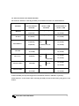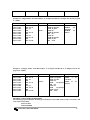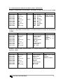
1
8255A – STUDY CARD
1.
INTRODUCTION
Electro Systems Associates Private Limited (ESA) manufactures trainers for most of the popular
microprocessors viz 8085, Z-80, 8031 8086/88, 68000 and 80196. ESA offers a variety of modules, which
can be interfaced, to these trainers. These modules can be effectively used for teaching/ training in the
Laboratories.
The 8255A PPI card incorporates Intel’s 8255A. This Interface is designed to explain all the facilities
available in 8255A.
Functional description of 8255A, implementation of the circuit and some simple software programs are
presented in this manual.
2.
DESCRIPTION OF THE CIRCUIT
The interface has 4 Dipswitches mentioned as SW1, SW2, SW3 and SW4. The 8255A port A and port B
can be configured in software as output by using the control word and keeping the switches SW1 and SW3
in O/P position and switches SW2 and SW4 will have no effect. Configure 8255A port A as input in
software while keeping SW1 in I/P position. After executing the program it reads the status of SW2
position. Similarly for port B, configure 8255A port B as input in software while keeping SW3 in I/P
position. After executing the program it reads the status of SW4 position. 8 RED LEDs are provided to
read the status of port A and 8 GREEN LEDs are provided to read the status of port B and YELLOW
LEDs are provided to read the signal status mentioned on the interface.
Switches S1, S2 and S3 are provided to simulate STB* or ACK* signals in Mode 1 and in Mode 2.
Provision is made for connecting buffered external interrupt (RST 7.5 etc.,) to J5 and keeping the jumper
JP2 at PC0 or PC3 depending on the type of Mode. The interface has got 4 connectors named as J2, J3, J4
and P1. J3 and J4 are reserved for MPS85-2 trainer and P1 is reserved for ESA85-2 trainer. All the 24
I/O lines are brought out to the J2 connector. But port C lines are used as handshake signals so user
cannot use those lines. (Only port A and port B lines are available to user).
8255A STUDY CARD USER MANUAL
1
3.0 INSTALLATION AND CONFIGURATION
The Connector details for connecting the Study Card to different Trainers are mentioned below.
CONNECTORS ON
TRAINER
MPS 85-3
ESA 85-2
CONNECTORS ON
STUDY CARD
CONNECTORS ON
TRAINER
ADAPTER
STUDY CARD
J3 (26 PIN)
No Adapter required
J3 (26 PIN)
J4 (26 PIN)
P1 (50 PIN)
J4 (26 PIN)
No Adapter required
J1 (50 PIN)
ESA 86/88-2/3 *
J1 (50 PIN)
PIN)
J2 (50 PIN)
J2 (50 PIN)
P1 (50 PIN)
J3 (26
J3 (26 PIN)
J4 (26
J4 (26 PIN)
PIN)
ESA 86E
J6 (26 PIN)
No Adapter required
J7 (26 PIN)
J4 (26 PIN)
J1(50 PIN)
ESA 31/51 *
J5(50 PIN)
J3(26
PIN)
J4(26 PIN)
P3(50 PIN)
ESA51E VER.3 *
J4(50 PIN)
P1(26 PIN)
P2(26
PIN)
ESA 51E VER.4
J4 (26 PIN)
J6 (26 PIN)
J3 (26 PIN)
No Adapter required
J3 (26 PIN)
J4 (26 PIN)
J3 (26 PIN)
J4 (26 PIN)
J3 (26 PIN)
J4 (26 PIN)
* External Study Card Adapter is required to connect the Study Card with the Trainer
Connect the Study Card by following the above-mentioned connectors with FRCs respectively.
Switch Off Power to the Trainer while connecting the Study Card. Press Reset after giving power to the
Trainer.
8255A STUDY CARD USER MANUAL
2
8255A
PROGRAMMABLE PERIPHERAL INTERFACE
The Intel 8255A is a general-purpose programmable, parallel I/O device designed for use with Intel
Microprocessor. It can be programmed to transfer data under various conditions from simple I/O to
Interrupt I/O.
The 8255A has 24 I/O PINS that can be grouped primarily in two 8 Bit parallel ports A & B, with the
remaining 8 bits as port C. The 8 bits of port can be used as individual bits or be grouped in two 4bit ports.
C upper and C lower. The functions of these ports are defined by writing a control word in the control register.
Figure 1 shows all the functions of 8255A, classified according to two modes: the Bit Set/Reset (BSR)
mode and the I/O mode. The I/O mode is further divided into three modes: Mode 0, Mode 1, and Mode 2. .
In mode 0, all ports function as simple I/O ports. Mode 1 is a handshake mode whereby ports A and /or B
use bits from port C as handshake signals. In the handshake mode, two types of I/O data transfer can be
implemented: status checks and interrupt. In Mode 2, port A can be set up for bi-directional data transfer
using handshake signals from port C, and port B can be set up either in Mode 0 or Mode 1.
8255A Modes
D7
D6
D5
D4
D3
D2
D1
D0
0/1
BSR Mode
(Bit Set/Reset)
For Port C
No effect on
I/O Mode
I/O Mode
Mode 0
Simple I/O
For ports
A, B & C
Mode 1
handshake
I/O for
Ports A & B
Port C bits
are used for
handshake
Mode 2
Bi-directional
Data bus for port A
Port B either
in Mode 0 or 1
Port C bits
are used for
handshake
FIG-1
8255A STUDY CARD USER MANUAL
3
The BSR Mode is used to set or reset the bits in port C. The I/O mode is further divided into three modes.
Mode 0, Mode 1 and Mode 2. In Mode 0 all ports functions as simple I/O ports. Mode 1 is a Handshake
mode where by ports A&B use bits from port C as Handshake signals.
BLOCK DIAGRAM OF THE 8255A
POWER
SUPPLIES
+5V
GND
8 bit internal
BI-DIRECTIONAL Data
DATA BUS
Bus
D7 D 0
Buffer
RD*
WR*
A1
A0
Read
Write
Control
Logic
Group
A
Control
Group
A
PORT
A
(8)
Group
A
PORT C
Upper
(4)
I/O
PA7-PA0
I/O
PC7-PC4
data bus
Group
B
PORT C
Lower
(4)
Group
B
Control
RESET
Group
B
PORT
B
(8)
I/O
PC3-PC0
I/O
PB7-PB0
CS*
FIG-2
The block diagram shows two 8 bit ports (A&B) and two 4 bit ports ((C U and CL ), the data bus buffer and
control logic.
CONTROL LOGIC:
The control section has six lines. Their functions and connections are as follows
.
RD * (Read) : This control signal enables the Read operation When the signal is low, the CPU reads
data from a selected I/O port of the 8255A.
WR* (Write) : This control signal enables the write operation. When the signal goes low, the CPU writes
into a selected I/O port or the control register.
8255A STUDY CARD USER MANUAL
4
RESET (Reset): This is an active high signal, it clears the control register and sets all ports in the input
mode.
CS*, A0 and A1: These are device select signals. CS* is connected to a decoded address and A0 & A1 are
generally connected to CPU address lines A0 & A1 respectively. The 8255A BASIC operation is given in
table 1.
Control word Format
Figure 3 shows a register called the control register. The contents of this register, called the Control word,
specify an I/O function for each port. This register can be accessed to write a control word when A0 and
A1 are at logic 1, as mentioned previously. The register is not accessible for a Read operation.
Bit D7 of the control register specifies either the I/O function or the Bit Set/Reset function, as
classified in Figure 3. If bit D7=1, bits D6-D0 determine I/O functions in various modes, as shown in
Figure fig-3. If bit D7=0, port C operates in the Bit Set/Reset (BSR) mode. The BSR control word does
not affect the functions of ports A and B (the BSR mode will be described later).
To communicate with peripherals through the 8255A, three steps are necessary:
Determine the addresses of ports A, B, and C and of the control register according to the Chip Select logic
and address lines A0 and A1.
Write a control word in the control register.
Write I/O instructions to communicate with peripherals through ports A, B, and C.
Control word
D7
D6
D5
D4
D3
D2
D1
D0
Group B
Port C (Lower-PC3PC0)
1=Input
0=Output
Port B
1=Input
0=Output
Mode Selection
0=Mode 0
1=Mode 1
Group A
Port C (Upper-PC7PC4)
1=Input
0=Output
Port A
1=Input
0=Output
Mode Selection
8255A STUDY CARD USER MANUAL
5
00=Mode 0
01=Mode 1
1X=Mode 2
1=I/O Mode
0=BSR Mode
FIG -3
8255A BASIC OPERATION
A1
0
0
1
A0
0
1
0
RD*
0
0
0
WR*
1
1
1
CS*
0
0
0
0
0
1
1
0
1
0
1
1
1
1
1
0
0
0
0
0
0
0
0
X
1
X
X
1
X
X
0
1
X
1
1
1
0
0
INPUT OPERATION (READ)
PORT A => DATA BUS
PORT B => DATA BUS
PORT C = >DATA BUS
OUTPUT OPERATION (WRITE)
DATA BUS => PORT A
DATA BUS => PORT B
DATA BUS => PORT C
DATA BUS = >CONTROL
DISABLE FUNCTION
DATA BUS => 3 STATE
ILLEGAL CONDITION
DATA BUS => 3 STATE
8255A OPERATIONAL DESCRIPTION
Mode 0 (Basic Input/Output): This
functional configuration provides simple Input and Output
operations for each of the three ports. No handshaking is required.
MODE 0 Basic Functional Definitions:
Two 8-bit ports and two 4-bit ports.
Any port can be input or output.
Outputs are latched.
Inputs are not latched.
16 different Input / Output configurations are possible in this Mode.
MODE 1 (Strobed Input / Output). This functional configuration provides a means for transferring I/O
data to or from a specified Port in conjunction with strobes or “handshaking” signals. In mode 1, Port A
and Port B use the lines on Port C to generate or accept these “handshaking” signals.
Mode 1 Basic Functional Definitions:
Two Groups (Group A and Group B).
Each group contains one 8-bit data port and one 4-bit control / data port.
The 8-bit data port can be either input or output. Both inputs and outputs are latched.
The 4-bit port is used for control and status of the 8-bit data port.
Input Control Signal Definition
STB (Strobe Input). A “low” on this input loads data into the input latch.
8255A STUDY CARD USER MANUAL
6
IBF (Input Buffer Full F / F)
A “high” on this output indicates that the data has been loaded into the input latch; in essence, an
acknowledgement IBF is set by STB input being low and is reset by the rising edge of the RD Input.
INTR (Interrupt Request)
A “high” on this output can be used to interrupt the CPU when an input device is requesting service.
INTR is set by the STB* is a one”, IBF is a “one” and INTE is a “one”. It is reset by the falling edge of
RD*. This procedure allows an input device to request service from the CPU by simply strobing its data
into the port.
INTE A
Controlled by bit set / reset of PC4.
INTE B
Controlled by bit set / reset of PC2.
Output Control Signal Definition
OBF* (Output Buffer Full F/F). The OBF output will go “low” to indicate that the CPU has written data
out to the specified port. The OBF F/F will be set by the rising edge of the WR input and reset by ACK
input being low.
ACK*(Acknowledge input). A “low” on this input informs the 8255A that the data from port A or port B
has been accepted. In essence, a response from the peripheral device indicating that it has received the
data output by the CPU.
INTR (Interrupt Request). A “high” on this output can be used to interrupt the CPU when an output
device has accepted data transmitted by the CPU. INTR is set when ACK is a “one”, OBF is a “one”. It is
reset by the falling edge of WR.
INTE A
Controlled by bit set/reset of PC6.
INTE B
Controlled by bit set/reset of PC2.
MODE 2 (Strobed Bi-directional Bus I/O). This functional configuration provides a means for
communicating with a peripheral device or structure on a single 8-bit bus for both transmitting and
receiving data (bi-directional bus I/O). “Handshaking” signals are provided to maintain proper bus flow
discipline in a similar manner to MODE 1. Interrupt generation and enable/disable functions are also
available.
MODE 2 Basic Functional Definitions:
Used in Group A only.
One 8-bit, bi-directional bus Port (Port A) and a 5-bit control Port (Port C).
Both inputs and outputs are latched.
The 5-bit control port (Port C) is used for control and status for the 8-bit, bi-directional bus port
(Port A).
Control Signal Definition Bi-directional Bus I/O
INTR (Interrupt Request). A high on this output can be used to interrupt the CPU for both input or
output operations.
Output Operations
8255A STUDY CARD USER MANUAL
7
OBF* (Output Buffer Full). The OBF output will go “low” to indicate that the CPU has written data out
to port A.
ACK* (Acknowledge). A “low” on this input enables the tri-state output buffer of port A to send out the
data. Otherwise, the output buffer will be in the high impedance state.
INTE 1 (The INTE Flip-Flop Associated with OBF). Controlled by bit set/reset of PC 6.
Input Operations
STB* (Strobe Input)
STB (Strobe input). A “low” on this input loads data into the input latch.
IBF (Input Buffer Full F/F). A “high” on this output indicates that data has been loaded into the input
latch.
INTE 2 (The INTE Flip-Flop Associated with IBF). Controlled by bit set/reset of PC4.
8255A STUDY CARD USER MANUAL
8
4.
DEMONSTRATION PROGRAMS FOR 8085 SERIES KIT
4A : DEMONSTRATION PROGRAMS FOR MPS 85-3 TRAINERKIT
Example 1:
Configure 8255A such that Port A & Port B as an Output Port. Execute the program at 8000H.
Port A
EQU
Port B
EQU
Control Register EQU
ADDRESS
OPCODE
8000
8002
8004
8006
8008
800A
800C
3E
D3
3E
D3
3E
D3
C3
80
83
55
80
AA
81
04
LABLE
BACK:
80
80H
81H
83H
MNEMONIC
COMMENTS
MVI
OUT
MVI
OUT
MVI
OUT
JMP
Port A and Port B as
an Output Port.
Output 55 to Port A
(Corresponding
LEDs
glows).
Output AA to Port B
(Corresponding
LEDs
glows).
Repeat the same.
A,80
83
A,55
80
A,AA
81
BACK
Example 2:
Configure 8255A such that Port A as on Output and Port B as an Input. Execute the program at 8000H.
ADDRESS
OPCODE
8000
8002
8004
8006
8008
3E
D3
DB
D3
EF
LABLE
82
83
81
80
MNEMONIC
COMMENTS
MVI
OUT
IN
OUT
RST
PortB as Input and
PortA as Output.
ReadtheDipSwitchesthr
oughportB.
Output to Port A
Stop the Program.
A,82
83
81
80
5
Example 3:
Configure 8255A such that Port A as an Input and Port B as an Output. Execute the program at 8000H.
ADDRESS
OPCODE
8000
8002
8004
8006
8008
3E
D3
DB
D3
EF
LABLE
90
83
80
81
MNEMONIC
COMMENTS
MVI
OUT
IN
OUT
RST
Port A as Input and Port B as
Output.
Read the Dipswitches through
Port B.
Output to Port B.
Stop the Program.
A,90
83
80
81
5
SINGLE BIT SET/RESET FEATURE
8255A STUDY CARD USER MANUAL
9
Important Note: Any of the eight bits of Port C can be set or reset using a single OUT instruction. But
before that user will have to initialize 8255 in an out put mode because during reset condition 8255 ports
are in input mode.
EXAMPLE 4 : PROGRAMS FOR BSR MODE
Write a BSR control word to set bits PC7 and reset them after certain delay.
ADDRESS
8000
8002
8004
8006
8008
800B
800D
800F
8010
8012
8014
8015
8018
8019
OPCODE
3E 80
D3 83
3E 0F
D3 83
CD 10 80
3E 0E
D3 83
76
3E FF
0E FF
0D
C2 14 80
3D
C2 12 80
C9
LABLE
DELAY:
L2:
L1:
MNEMONIC
MVI A, 80H
OUT 83
MVI A, 0FH
OUT 83
CALL DELAY
MVI A, 0EH
OUT 83H
HLT
MVI A,0FFH
MVI C,0FFH
DCR C
JNZ L1
DCR A
JNZ L2
RET
COMMENTS
SET PC7
SOME DELAY
RESET PC7
From the analysis of the routine the following points can be noted.
1) To Set/Reset bits in port C, a control word is written in the control register and not in port C
2) BSR control word affects only one bit in port C
3) The BSR control word does not affect the I/O mode.
EXAMPLE 5: PROGRAMS FOR MODE 1
NOTE: For testing the Mode 1 and Mode 2 operation, connect buffered external interrupt to J5 of the
interface.
1. The following program initializes 8255A Port A as on Input in Mode 1 and Port B as an Output in Mode
0.
Read through Input & Output to the data field of the trainer display. If you change the Input and the
same will be repeated at data field & Port B. Press S2 switch to simulate STB A* signal.
Note: Put the jumper at PC3 connect External interrupt from J4 of pin 7 ( i.e RST 5.5 ) to J5 of interface.
8255A STUDY CARD USER MANUAL
10
ADDRESS
8000
8002
8004
8006
8008
800A
800B
800C
OPCODE
3E B0
D3 83
3E 09
D3 83
3E 0E
30
FB
C3 0C 80
8FB3
C3 00 90
9000
9002
9004
9006
9009
900C
DB
D3
06
32
CD
C3
80
81
00
F1 8F
4C 04
00 90
LABLE
Loop:
UP:
MNEMONIC
MVI A, B0
OUT 83
MVI A, 09
OUT 83
MVI A, 0E
SIM
EI
JMP Loop
JMP
9000
IN
OUT
MVI
STA
CALL
JMP
80
81
B, 00
8FF1
044C
UP
COMMENTS
PortA as input in Mode1
Set INTEA.
Enable RST 5.5.
Read through Port A and
Output to port B
&
display it on
data field
of the trainer display.
Example 6: The following program initializes 8255 Port B as Input in Mode 1 and Port A as on Output in
Mode 0. Read through Port B and Output to Port A as well as data field of the trainer display the
program is in a continuous loop. If you change the Input the same thing will be repeated at Port B LEDs
as well as data field of the trainer display. Press S1 switch to simulate STB B* signal.
Note: Put the jumper at PC0. Connect external interrupt from J4 of pin 7 (i.e RST 5.5) to J5 of interface.
ADDRESS
OPCODE
8000
8002
8004
8006
8008
800A
800B
800C
3E
D3
3E
D3
3E
30
FB
C3
8FB3
C3 00 90
9000
9002
9004
9006
9009
900C
DB
D3
06
32
CD
C3
LABLE
MNEMONIC
COMMENTS
A,86
83
A,05
83
A,0E
PortB as an input in Mode1 &
Port A as an output in Mode0
Set INTEB
Loop:
MVI
OUT
MVI
OUT
MVI
SIM
EI
JMP
JMP
9000
IN
OUT
MVI
STA
CALL
JMP
81
80
B, 00
8FF1
044C
UP
86
83
05
83
0E
0C 80
81
80
00
F1 8F
4C 04
00 90
UP:
Enable RST 5.5
Loop
Read through Port B and
output to Port A and display
it on data field of the
the trainer display
Example 7: The following program initializes 8255 Port A as an Input in Mode1 and Port B as an Output
in Mode 0. Read through Input and Output to the data field of the trainer display. Press S2 switch to
simulate STBA*.
Note: Put the jumper at PC3. Connect external interrupt from pin 3 of J3 (i.e. Buffered RST 6.5) to J5 of
interface.
ADDRESS
OPCODE
LABLE MNEMONIC
COMMENTS
8000
8002
3E B0
D3 83
8255A STUDY CARD USER MANUAL
MVI
OUT
A, B0
83
PortA as an input in Mode1
&
11
8004
8006
8008
800A
800B
800C
3E
D3
3E
30
FB
C3
09
83
0D
8FB9
C3 00 90
9000
9002
9004
9006
9009
900C
DB
D3
06
32
CD
C3
0C 80
80
81
00
F1 8F
4C 04
00 90
Loop:
UP:
MVI
OUT
MVI
SIM
EI
JMP
A, 09
83
A, 0D
JMP
9000
PortB as an output in Mode
0
Set INTEA
Enable RST 6.5
Loop
IN
80
OUT 81
MVI B, 00
STA 8FF1
CALL 044C
JMP UP
Read through Port A &
output to port B
&
display it on data field of
the trainer display
Example 8: The following program initializes 8255A Port B as Input in Mode 1 and Port A as an Output in
Mode 0 Read through Port B and Output to Port A as well as data field of the trainer display press S1
switch to simulate STBB* signal.
Note:Put the jumper at PC0. Connect external interrupt from pin3 of J3. (i.e.RST6.5) to J5 of interface
ADDRESS
8000
8002
8004
8006
8008
800A
800B
800C
OPCODE
3E 86
D3 83
3E 05
D3 83
3E 0D
30
FB
C3 0C 80
8FB9
C3 00 90
9000
9002
9004
9006
9009
900C
DB
D3
06
32
CD
C3
81
80
00
F1 8F
4C 04
00 90
LABLE
Loop:
MNEMONIC
MVI A, 86
OUT 83
MVI A, 05
OUT 83
MVI A, 0D
SIM
EI
JMP Loop
JMP
UP:
COMMENTS
PortB as an input &
PortA as an output
Set INTEB,
Enable RST 6.5
9000
IN
81
OUT 80
MVI B, 00
STA 8FF1
CALL 044C
JMP UP
Read through portB &
output through portA
&
display it on datafield
of
the trainer display.
Example 9:. The following program initializes 8255 Port A as an Input in Mode 2 and Port B as Output in
Mode 0 press S2 switch.
Note: Put the jumper at PC3 connect external interrupt RST 6.5 signal to J5 of interface S2 switch to
simulate STBA*.
ADDRESS
8000
8002
8004
8006
8008
800A
OPCODE
3E D0
D3 83
3E 09
D3 83
3E 0D
30
LABLE
8255A STUDY CARD USER MANUAL
MNEMONIC
MVI A, D0
OUT 83
MVI A, 09
OUT 83
MVI A, 0D
SIM
COMMENTS
PortA as on input in Mode2 &
portB as on output in Mode 0
Set INTEA
Enable RST 6.5
12
800B
800C
FB
C3 0C 80
8FB9
C3 00 90
9000
9002
9004
9006
9009
900C
DB
D3
06
32
CD
C3
80
81
00
F1 8F
4C 04
00 90
Loop:
UP:
EI
JMP
Loop
JMP
9000
IN
80
OUT 81
MVI B, 00
STA 8FF1
CALL 044C
JMP UP
Read through port A &
output through port B
&
display it on data field of
the trainer display
Example 10: The following program initializes 8255A Port B as an Output in Mode1 press S1 switch to
simulate ACKB*.
Note: Put the jumper at PC3 and connect external interrupt RST 7.5 signal to J5 of interface.
ADDRESS
OPCODE
LABLE
MNEMONIC
COMMENTS
8000
8002
8004
8006
8008
800A
800B
800C
3E
D3
3E
D3
3E
30
FB
C3
A4
83
05
83
1B
A, A4
83
A, 05
83
A, 1B
Port B an output in Mode
1.
Loop:
MVI
OUT
MVI
OUT
MVI
SIM
EI
JMP
8FBF
C3
00 90
JMP
9000
9000
9002
9004
9006
9009
900B
3E
06
32
CD
D3
C3
55
00
F1 8F
4C 04
81
00 90
MVI A, 55
MVI B, 00
STA 8FF1
CALL 044C
OUT 81
JMP UP
0C 80
UP:
Set INTEB.
Enable RST 7.5.
Loop
Load Accumulator with 55
& display it on datafield
of the trainer display. &
On the corresponding LEDs
of port B
Example 11: The following program initializes 8255A Port A as on Output in Mode1. Use RST 7.5 as an
interrupt signal press switch to simulate ACKA*.
Note: Put the jumper at PC3 and connect external interrupt RST 7.5 signal to J5 of interface.
ADDRESS
OPCODE
8000
8002
8004
8006
8008
3E
D3
3E
D3
3E
LABLE
A0
83
0D
83
1B
8255A STUDY CARD USER MANUAL
MNEMONIC
COMMENTS
MVI
OUT
MVI
OUT
MVI
PortA
Mode1
A, A0
83
A, 0D
83
A, 1B
as
an
output
in
Set INTEA
13
800A
800B
800C
30
FB
C3 0C 80
8FBF
C3 00 90
9000
9002
9004
9006
9009
900B
3E
06
32
CD
D3
C3
55
00
F1 8F
4C 04
80
00 90
Loop:
UP:
SIM
EI
JMP
Enable RST 7.5
Loop
JMP
9000
MVI A, 55
MVI B, 00
STA 8FF1
CALL 044C
OUT 80
JMP UP
Load Accumulator with 55
& display it on datafield
of the trainer display &
On the corresponding LEDs
of port A
Example 12: The following program initializes 8255A Port A as an Input in Mode1 and Port B as an
output in Mode 0. Press S2 switch to simulate STB A*.
Note: Put the jumper at PC0 connect external interrupt RST 7.5 signal to J5 of interface.
ADDRESS
OPCODE
8000
8002
8004
8006
8008
800A
800B
800C
3E
D3
3E
D3
3E
30
FB
C3
8FBF
C3 00 90
9000
9002
9004
9006
9009
900C
DB
D3
06
32
CD
C3
LABLE
MNEMONIC
COMMENTS
A, B0
83
A, 09
83
A, 1B
PortA as an input in Mode1
PortB as an output in
Mode0. Set INTEA
Loop:
MVI
OUT
MVI
OUT
MVI
SIM
EI
JMP
JMP
9000
IN
OUT
MVI
STA
CALL
JMP
80
81
B, 00
8FF1
044C
UP
B0
83
09
83
1B
0C 80
80
81
00
F1 8F
4C 04
00 90
UP:
Enable RST 7.5
Loop
Read through Port A &
output to Port B
&
display it on at data
field
of
the
trainer
display
Example 13: The following program initializes 8255A Port B as an Input in Mode1 and Port A as an
output in Mode 0. Press S1 switch to simulate STB B*.
Note: Put the jumper at PC0 connect external interrupt RST 7.5 signal to J5 of interface.
ADDRESS
OPCODE
8000
8002
8004
8006
8008
800A
3E
D3
3E
D3
3E
30
LABLE
86
83
05
83
1B
8255A STUDY CARD USER MANUAL
MNEMONIC
COMMENTS
MVI
OUT
MVI
OUT
MVI
SIM
PortB as an input in
Mode1.PortA as an output
in Mode0.
Set INTEB
A, 86
83
A, 05
83
A, 1B
Enable RST 7.5
14
800B
800C
FB
C3 0C 80
8FBF
C3 00 90
9000
9002
9004
9006
9009
900C
DB
D3
06
32
CD
C3
81
80
00
F1 8F
4C 04
00 90
Loop:
UP:
EI
JMP
Loop
JMP
9000
IN
OUT
MVI
STA
CALL
JMP
81
80
B, 00
8FF1
044C
UP
Read through Port B &
Output to Port A
&
display it on datafield
of the trainer display
8255A MODE 2 Bi-directional Input/Output
Example 14: The following program initializes 8255 in Mode 2 .
Press S3 switch to simulate ACKA*.
Note: Put the jumper at PC3. Connect external interrupt from JP10 (i.e RST 7.5) to J5 of interface.
ADDRESS
OPCODE
8000
8002
8004
8006
8008
800A
800B
800C
3E
D3
3E
D3
3E
30
FB
C3
FE12
C3 00 90
9000
9002
9004
9006
9009
900C
900E
9010
DB
D3
06
32
CD
3E
D3
C3
LABLE
MNEMONIC
COMMENTS
A, C0
83
A, 0D
83
A, 1B
PortA as an output in Mode2
Loop:
MVI
OUT
MVI
OUT
MVI
SIM
EI
JMP
JMP
9000
C0
83
0D
83
1B
0C 80
80
81
00
75 FE
78 05
F0
80
00 90
UP:
Set INTE1
Enable RST 7.5
Loop
IN 80
OUT 81
MVI B, 00
STA FE75
CALL 0578
MVI
A,F0
OUT 80
JMP UP
READ DIP SWITCH2 POSITION
AND DISPLAY IT ON THE DATA
FIELD OF THE TRAINER AND ON
THE PORT B LEDs.
SHOW F0 ON PORT A LEDS .
AFTER PUTINGING DIPSWITCH 1
IN OFF POSITION AND THEN
PRESSING AND HOLDING S3.
FOLLOWING PROCEDURE SHOULD BE FOLLOWED FOR USING THIS PROGRAM IN MODE 2
1.
KEEP DIP SWITCH 1 IN ON POSITION AND DIP SWITCH 2 IN POSITION
CORRESPONDING TO THE DATA WHICH U WANT TO SEND AS IN PUT FROM PORT A.
2.
INTERRUPT 7.5
3.
KEEP DIP SWITCH1 IN OFF POSITION
8255A STUDY CARD USER MANUAL
15
4.
PRESS S3 AND HOLD IT .THE CORRESPONDING PORT A LEDs WILL SHOW F0. THIS
DISPLAY CAN BE CHANGED BY CHANGING THE OPERAND OF MVI A INSTRUCTION
AT MEMORY LOCATION 900C IN ABOVE PROGRAM .
NOTE : DON’T PRESS S1 OR S2 SWITCH AFTER PUTTING DIP SWITCH 1 IN OFF
POSITION.
WHILE PRESSING AND HOLDING S3 YOU CAN SEE THAT THE PORT A
WORKING AS OUTPUT PORT.
4B: DEMONSTRATION PROGRAMS FOR ESA 85-2 TRAINER KIT
RAM addresses for Interrupts
RST 5.5
FE06H
RST 6.5
FE0CH
RST 7.5
FE12H
Example 1:
Configure 8255A such that Port A & Port B as an Output Port. Execute the program at 8000H.
Port A
EQU
80H
Port B
EQU
81H
Control Register EQU
83H
ADDRESS
OPCODE
8000
8002
8004
8006
8008
800A
800C
3E
D3
3E
D3
3E
D3
C3
80
83
55
80
AA
81
04
LABLE
BACK:
80
MNEMONIC
COMMENTS
MVI
OUT
MVI
OUT
MVI
OUT
JMP
Port A and Port B as
an Output Port.
Output 55 to Port A
(Corresponding
LEDs
glows).
Output AA to Port B
(Corresponding
LEDs
glows).
Repeat the same.
A,80
83
A,55
80
A,AA
81
BACK
Example 2:
Configure 8255A such that Port A as on Output and Port B as an Input. Execute the program at 8000H.
ADDRESS
OPCODE
8000
8002
8004
8006
8008
3E
D3
DB
D3
DF
82
83
81
80
LABLE
MNEMONIC
COMMENTS
MVI
OUT
IN
OUT
RST
PortB as Input and PortA as
Out put.Read the Dip Switches
through port B. Output
to
Port A Stop the Program.
8255A STUDY CARD USER MANUAL
A,82
83
81
80
3
16
Example 3:
Configure 8255A such that Port A as an Input and Port B as an Output. Execute the program at 8000H.
ADDRESS
OPCODE
8000
8002
8004
8006
8008
3E
D3
DB
D3
DF
90
83
80
81
LABLE
MNEMONIC
COMMENTS
MVI
OUT
IN
OUT
RST
Port A as Input and Port B as
Output.
Read the Dipswitches through
PortB.
Output to Port B.
Stop the Program.
A,90
83
80
81
3
SINGLE BIT SET/RESET FEATURE
Any of the eight bits of Port C can be set or reset using a single OUT instruction. But before that user will
have to initialize 8255 in an out put mode, because during reset condition, the 8255 ports will be in input
mode.
Example 4: PROGRAMS FOR BSR MODE
Write a BSR control word to set bits PC7 and reset them after certain delay.
ADDRESS OPCODE
LABLE
MNEMONIC
COMMENTS
8000
3E 80
MVI A, 80H
8002
D3 83
OUT 83
8004
3E 0F
MVI A, 0FH
8006
D3 83
SET PC7
OUT 83
8008
CD 10 80
CALL DELAY SOME DELAY
800B
3E 0E
MVI A, 0EH
800D
D3 83
RESET PC7
OUT 83H
800F
76
HLT
8010
3E FF
DELAY: MVI A,0FFH
8012
0E FF
L2:
MVI C,0FFH
8014
0D
L1:
DCR C
8015
C2 14 80
JNZ L1
8018
3D
DCR A
8019
C2 12 80
JNZ L2
C9
RET
From the analysis of the routine the following points can be noted.
1) To Set/Reset bits in port C, a control word is written in the control register and not in port C
2) BSR control word affects only one bit in port C
3) The BSR control word does not affect the I/O mode.
Example 5: PROGRAMS FOR MODE 1
NOTE: For testing the Mode 1 and Mode 2 operation, connect buffered external interrupt to J5 of the
interface.
1. The following program initializes 8255A Port A as on Input in Mode 1 and Port B as an Output in Mode
0.
Read through Input & Output to the data field of the trainer display. If you change the Input and the
same will be repeated at data field & Port B. Press S2 switch to simulate STB A* signal.
Note: Put the jumper at PC3 connect External interrupt from JP12 of trainer ( i.e RST 5.5 ) to J5 of
interface.
ADDRESS
OPCODE
LABLE
MNEMONIC
COMMENTS
8000
3E B0
MVI A, B0
PortA as input in Mode1
8002
D3 83
OUT 83
8004
3E 09
MVI A, 09
Set INTEA.
8006
D3 83
OUT 83
8255A STUDY CARD USER MANUAL
17
8008
800A
800B
800C
3E 0E
30
FB
C3 0C 80
FE06
9000
9002
9004
9006
9009
900C
C3
DB
D3
06
32
CD
C3
00
80
81
00
75
78
00
Loop:
90
UP:
FE
05
90
MVI
SIM
EI
JMP
A, 0E
JMP
IN
OUT
MVI
STA
CALL
JMP
9000
80
81
B, 00
FE75
0578
UP
Enable RST 5.5.
Loop
Read through Port A and
Output to port B
&
display it on datafield of
the trainer display.
Example 6: The following program initializes 8255 Port B as Input in Mode 1 and Port A as on Output in
Mode 0. Read through Port B and Output to Port A as well as data field of the trainer display the
program is in a continuous loop. If you change the Input the same thing will be repeated at Port B LEDs
as well as data field of the trainer display. Press S1 switch to simulate STB B* signal.
Note: Put the jumper at PC0. Connect external interrupt from JP12 of trainer (i.e RST 5.5) to J5 of
interface.
ADDRESS
8000
8002
8004
8006
8008
800A
800B
800C
OPCODE
3E 86
D3 83
3E 05
D3 83
3E 0E
30
FB
C3 0C 80
FE06
C3 00 90
9000
9002
9004
9006
9009
900C
DB
D3
06
32
CD
C3
81
80
00
75 FE
78 05
00 90
LABLE
Loop:
UP:
MNEMONIC
MVI A,86
OUT 83
MVI A,05
OUT 83
MVI A,0E
SIM
EI
JMP Loop
JMP
9000
IN
OUT
MVI
STA
CALL
JMP
81
80
B, 00
FE75
0578
UP
COMMENTS
PortB as an input in Mode1 &
Port A as an output in Mode0
Set INTEB
Enable RST 5.5
Read through Port B and
output to Port A and display
it on data field of the
the trainer display
Example 7: The following program initializes 8255 Port A as an Input in Mode1 and Port B as an Output
in Mode 0. Read through Input and Output to the data field of the trainer display. Press S2 switch to
simulate STBA*.
Note: Put the jumper at PC3. Connect external interrupt from JP11 of trainer (i.e Bufferd RST 6.5) to J5
of interface.
ADDRESS
OPCODE
LABLE
MNEMONIC
COMMENTS
8000
8002
8004
8006
8008
3E
D3
3E
D3
3E
B0
83
09
83
0D
8255A STUDY CARD USER MANUAL
MVI
OUT
MVI
OUT
MVI
A, B0
83
A, 09
83
A, 0D
PortA as an input in Mode1 &
PortB as an output in Mode 0
Set INTEA
Enable RST 6.5
18
800A
800B
800C
30
FB
C3 0C 80
FE0C
C3 00 90
9000
9002
9004
9006
9009
900C
DB
D3
06
32
CD
C3
80
81
00
75 FE
78 05
00 90
Loop:
UP:
SIM
EI
JMP
Loop
JMP
9000
IN
80
OUT 81
MVI B, 00
STA FE75
CALL 0578
JMP UP
Read through Port A &
output to port B
&
display it on data field of
the trainer display
Example 8:The following program initializes 8255A Port B as Input in Mode 1 and Port A as an Output in
Mode 0 Read through Port B and Output to Port A as well as data field of the trainer display press S1
switch to simulate STBB* signal.
Note: Put the jumper at PC0. Connect external interrupt from JP11 of trainer (i.e. RST 6.5) to J5 of
interface.
ADDRESS
OPCODE
LABLE
MNEMONIC
COMMENTS
8000
8002
8004
8006
8008
800A
800B
800C
3E
D3
3E
D3
3E
30
FB
C3
86
83
05
83
0D
FE0C
C3 00 90
9000
9002
9004
9006
9009
900C
DB
D3
06
32
CD
C3
0C 80
81
80
00
75 FE
78 05
00 90
Loop:
UP:
MVI
OUT
MVI
OUT
MVI
SIM
EI
JMP
A, 86
83
A, 05
83
A, 0D
JMP
9000
PortB as an input &
PortA as an output
Set INTEB,
Enable RST 6.5
Loop
IN
81
OUT 80
MVI B, 00
STA FE75
CALL 0578
JMP UP
Read through port B &
output through port A
&
display it on data field
of
the trainer display.
Example 9: The following program initializes 8255 Port A as an Input in Mode 2 and Port B as Output in
Mode 0.
Note: Put the jumper at PC3 connect external interrupt from JP11 of trainer (i.e RST 6.5 signal) to J5 of
interface.
Press S2 switch to simulate STBA*.
ADDRESS
OPCODE
8000
8002
8004
8006
3E
D3
3E
D3
LABLE
D0
83
09
83
8255A STUDY CARD USER MANUAL
MNEMONIC
COMMENTS
MVI
OUT
MVI
OUT
PortA as on input in Mode2 &
PortB as on output in Mode 0
Set INTEA
A, D0
83
A, 09
83
19
8008
800A
800B
800C
3E 0D
30
FB
C3 0C 80
FE0C
C3 00 90
9000
9002
9004
9006
9009
900C
DB
D3
06
32
CD
C3
80
81
00
75 FE
78 05
00 90
Loop:
UP:
MVI
SIM
EI
JMP
A, 0D
JMP
9000
Enable RST 6.5
Loop
IN
80
OUT 81
MVI B, 00
STA FE75
CALL 0578
JMP UP
Read through port A &
Output through port B
&
display it on datafield of
the trainer display
Example 10:The following program initializes 8255A Port B as an Output in Mode1 press S1 switch to
simulate ACKB*.
Note: Put the jumper at PC3 and connect external interrupt from JP10 of trainer (i.e RST 7.5 signal) to J5
of interface.
ADDRESS
OPCODE
8000
8002
8004
8006
8008
800A
800B
800C
3E
D3
3E
D3
3E
30
FB
C3
FE12
C3 00 90
9000
9002
9004
9006
9009
900B
3E
06
32
CD
D3
C3
LABLE
MNEMONIC
COMMENTS
A, A4
83
A, 05
83
A, 1B
Port B an output in Mode 1.
Loop:
MVI
OUT
MVI
OUT
MVI
SIM
EI
JMP
JMP
9000
A4
83
05
83
1B
0C 80
55
00
75 FE
78 05
81
00 90
UP:
Set INTEB.
Enable RST 7.5.
Loop
MVI A, 55
MVI B, 00
STA FE75
CALL 0578
Out 81
JMP UP
Load Accumulator with 55
& display it on datafield of
the trainer display & On the
corresponding LEDs of port B
Example 11: The following program initializes 8255A Port A as on Output in Mode1. Use RST 7.5 as an
interrupt signal press switch S3 to simulate ACKA*.
Note: Put the jumper at PC3 and connect external interrupt from JP10 of trainer (i.e RST 7.5 signal )to J5
of interface.
ADDRESS
OPCODE
LABLE
MNEMONIC COMMENTS
8000
8002
8004
8006
8008
800A
800B
3E
D3
3E
D3
3E
30
FB
A0
83
0D
83
1B
8255A STUDY CARD USER MANUAL
MVI
OUT
MVI
OUT
MVI
SIM
EI
A, A0
83
A, 0D
83
A, 1B
PortA as an output in Mode1
Set INTEA
Enable RST 7.5
20
800C
C3 0C 80
FE12
C3 00 90
9000
9002
9004
9006
9009
900B
3E
06
32
CD
D3
C3
55
00
75 FE
78 05
80
00 90
Loop:
UP:
JMP
Loop
JMP
9000
MVI A, 55
MVI B, 00
STA FE75
CALL 0578
OUT 80
JMP UP
Load Accumulator with 55
& display it on datafield of
the trainer display & On the
corresponding LEDs of port A
Example 12: The following program initializes 8255A Port A as an Input in Mode1 and Port B as an
output in Mode 0. Press S2 switch to simulate STB A*.
Note: Put the jumper at PC3 connect external interrupt from JP10 of trainer (i.e RST 7.5 signal ) to J5 of
interface.
ADDRESS
OPCODE
8000
8002
8004
8006
8008
800A
800B
800C
3E
D3
3E
D3
3E
30
FB
C3
FE12
C3 00 90
9000
9002
9004
9006
9009
900C
DB
D3
06
32
CD
C3
LABLE
MNEMONIC
COMMENTS
A, B0
83
A, 09
83
A, 1B
PortA as an input in Mode1
Loop:
MVI
OUT
MVI
OUT
MVI
SIM
EI
JMP
JMP
9000
IN
OUT
MVI
STA
CALL
JMP
80
81
B, 00
FE75
0578
UP
B0
83
09
83
1B
0C 80
80
81
00
75 FE
78 05
00 90
UP:
Set INTEA
Enable RST 7.5
Loop
Read through Port A &
output to Port B
&
display it on at data field
of the trainer display
Example 13: The following program initializes 8255A Port B as an Input in Mode1 and Port A as an
output in Mode 0. Press S1 switch to simulate STB B*.
Note: Put the jumper at PC0 connect external interrupt from JP10 of trainer (RST 7.5 signal ) to J5 of
interface.
ADDRESS
OPCODE
LABLE
MNEMONIC COMMENTS
8000
8002
8004
8006
8008
800A
3E
D3
3E
D3
3E
30
86
83
05
83
1B
8255A STUDY CARD USER MANUAL
MVI
OUT
MVI
OUT
MVI
SIM
A, 86
83
A, 05
83
A, 1B
PortB as an input in Mode1
Set INTEB
Enable RST 7.5
21
800B
800C
FB
C3 0C 80
FE12
C3 00 90
9000
9002
9004
9006
9009
900C
DB
D3
06
32
CD
C3
81
80
00
75 FE
78 05
00 90
Loop:
UP:
EI
JMP
Loop
JMP
9000
IN
OUT
MVI
STA
CALL
JMP
81
80
B, 00
FE75
0578
UP
Read through Port B &
Output to Port A
&
display it on datafield of
the trainer display
8255A MODE2 Bi-directional Input/Output
Example 14: The following program initializes 8255 in Mode 2 .
Press S3 switch to simulate ACKA*.
Note: Put the jumper at PC3. Connect external interrupt from JP10 (i.e RST 7.5) to J5 of interface.
ADDRESS
OPCODE
8000
8002
8004
8006
8008
800A
800B
800C
3E
D3
3E
D3
3E
30
FB
C3
FE12
C3 00 90
9000
9002
9004
9006
9009
900C
900E
9010
DB
D3
06
32
CD
3E
D3
C3
LABLE
MNEMONIC
COMMENTS
A, C0
83
A, 0D
83
A, 1B
PortA as an output in Mode2
Loop:
MVI
OUT
MVI
OUT
MVI
SIM
EI
JMP
JMP
9000
C0
83
0D
83
1B
0C 80
80
81
00
75 FE
78 05
F0
80
00 90
UP:
Set INTE1
Enable RST 7.5
Loop
IN 80
OUT 81
MVI B, 00
STA FE75
CALL 0578
MVI
A,F0
OUT 80
JMP UP
READ DIP SWITCH2 POSITION
AND DISPLAY IT ON THE DATA
FIELD OF THE TRAINER AND ON
THE PORT B LEDs.
SHOW F0 ON PORT A LEDS .
AFTER PUTING DIPSWITCH 1 IN
OFF
POSITION
AND
THEN
PRESSING AND HOLDING S3.
FOLLOWING PROCEDURE SHOULD BE FOLLOWED FOR USING ABOVE PROGRAM IN MODE
2
1. KEEP DIP SWITCH 1 IN ON POSITION AND DIP SWITCH 2 IN POSITION
CORRESPONDING TO THE DATA WHICH U WANT TO SEND AS IN PUT FROM PORT A.
2.
INTERRUPT 7.5
3.
KEEP DIP SWITCH1 IN OFF POSITION
8255A STUDY CARD USER MANUAL
22
4.
PRESS S3 AND HOLD IT .THE CORRESPONDING PORT A LEDs WILL SHOW F0. THIS
DISPLAY CAN BE CHANGED BY CHANGING THE OPERAND OF MVI A INSTRUCTION
AT MEMORY LOCATION 900C IN ABOVE PROGRAM .
NOTE : DON’T PRESS S1 OR S2 SWITCH AFTER PUTTING DIP SWITCH 1 IN OFF POSITION.
WHILE PRESSING AND HOLDING S3 YOU CAN SEE THAT THE PORT A WORKING
AS OUTPUT PORT.
5 : DEMONSTRATION PROGRAMS FOR 8051 SERIES KIT
5A: EXAMPLE PROGRAM FOR ESA 31 TRAINER KIT
Configuration and Setting details:
For interfacing the study cards with ESA 31 trainers study card adapter is provided with the study cards.
Connect by using 50 pin FRC from Study card adapter to ESA 31 kit J5 connector. Connect by using two
26 pin FRC between J3 and J4 of study card adapter with the study card respectively
Connector J2 of 8255A Study Card can be interfaced with any ESA Interfaces (e.g. Logic Controller).
The interface derives its power via system connector. No external power supply is required. Provision is
made for external power supply also.
EXAMPLE PROGRAMS FOR ESA 31 TRAINERS IN MODE 0
Example 1: Configure 8255A such that Port A & Port B as an Output Port.
Execute the Program at
8000H
PORT A
= F180H
PORT B
= F181H
PORT C
= F182H
CTRL REG = F183H
ADDRESS
8000
8003
8005
8006
8009
800B
800C
800E
800F
8010
OPCODE
90 F1 83
74 80
F0
90 F1 80
74 55
F0
74 66
A3
F0
80 FE
LABLE
MNEMONIC
MOV DPTR,#F183
MOV A,#80
MOVX @DPTR,A
MOV DPTR,#F180
MOV A,#55
MOVX @DPTR,A
MOV A,#66
INC DPTR
MOVX @DPTR,A
SJMP 8010
COMMENTS
PORT A & B
AS
OUTPUT
PORTS
Example 2. Configure 8255A such that Port A as an Output & Port B as an Input
Execute the Program at 8000H
ADDRESS
OPCODE
8255A STUDY CARD USER MANUAL
LABLE
MNEMONIC
COMMENTS
23
8000
8003
8005
8006
8009
800A
800C
800D
90
74
F0
90
E0
15
F0
80
F1 83
82
MOV DPTR,#F183
MOV A,#82
MOVX @DPTR,A
MOV DPTR,#F181
MOVX A,@DPTR
DEC 82
MOVX @DPTR,A
SJMP 8006
F1 81
82
F7
PORT
A
AS
O/P PORT B
AS I/P
DPL=82
Example 3. Configure 8255A such that Port A as an Input & Port B as an Output. Execute the Program at
8000H
ADDRESS
OPCODE
LABLE
MNEMONIC
COMMENTS
8000
90 F1 83
MOV DPTR,#F183
8003
74 90
MOV A,#90
PORT
A
AS
8005
F0
MOVX @DPTR,A
I/P PORT B
8006
90 F1 80
MOV DPTR,#F180
AS O/P
8009
E0
MOVX A,@DPTR
800A
A3
INC DPTR
800B
F0
MOVX @DPTR,A
800C
80 F8
SJMP 8006
EXAMPLE PROGRAM OF BSR MODE
SINGLE BIT SET/RESET FEATURE
Any of the eight bits of Port C can be set or reset using a single OUT instruction. But before that
programmer will have to initialize 8255 in any input/out put mode.
Example 4 : PROGRAMS FOR BSR MODE
Write a BSR control word to set bits PC7 and reset them after certain delay. This is a continuous loop
PC7 will set and reset continuously.
ADDRESS
8000
8002
8005
8006
8008
8009
800c
800D
800E
8011
OPCODE
74 80
90 F1 83
F0
74 0F
F0
12 80 13
14
F0
12 80 13
80 80 06
8013
8015
8017
7F
7E
DE
DF
32
FF
FF
FE
FA
LABLE
MNEMONIC
MOV A,#80
MOV DPTR,#0F183
MOVX @DPTR,A
MOV
A,#0F
MOVX
@DPTR,A
LCALL 8013
DEC
A
MOVX
@DPTR,A
LCALL 8013
SJMP
8006
MOV
MOV
DJNZ
DJNZ
RET
R7,#0FF
R6,#0FF
R6,8017
R7,8015
COMMENTS
CALL DELAY
CALL DELAY
DELAY SUB
RUTINE
From the analysis of the routine the following points can be noted.
1) To Set/Reset bits in port C, a control word is written in the control register and not in port C
2) BSR control word affects only one bit in port C
8255A STUDY CARD USER MANUAL
24
3) The BSR control word does not affect the I/O mode.
EXAMPLE PROGRAMS FOR MODE 1
NOTE: For testing the Mode 1 and Mode 2 operation, Connect buffered external interrupt to J5 of the
interface.
Example 5: The following program initializes 8255 Port A as Input configuration in Mode 1.
through the Port A(Input) , output to the Port B.
Reading
If you change the input the same thing will be repeated. Press S2 switch. To simulate STB A * signal
NOTE: Put the jumper at PC3.
ADDRESS
8000
8003
8005
8006
8008
8009
800C
FFF3
9000
9003
9004
9007
9008
INTERRUPT ENABLE REGISTER ADDRESS IS = 0A8
OPCODE
90 F1 83
74 B0
F0
74 09
F0
75 A8 84
80 FE
LABLE
MNEMONIC
MOV DPTR,#F183
MOV A,#0B0
MOVX @DPTR,A
MOV A,#09
MOVX @DPTR,A
MOV 0A8,#84
SJMP 800C
02 90 00
LJMP 9000
90 F1 80
EO
90 F1 81
F0
02 90 00
MOV DPTR,#F180
MOVX A,@DPTR
MOV DPTR,#F181
MOVX @DPTR,A
SJMP 9000
COMMENTS
INITIALIZE
8255 PORT A AS
INPUT IN MODE1
SET INTEA
ENABLE
INTERRUPT
Example 6: The following program initializes 8255 Port B as Input configuration in Mode 1. Reading
through Port B and Output to Port A .
If you change the input the same thing will be repeated at Port A LEDs. Press S1 switch to simulate STB B
* signal.
Note: Put the jumper at PC0.
ADDRESS
OPCODE
8000
8003
8005
8006
8008
8009
800c
90
74
F0
74
F0
75
80
INTERRUPT ENABLE REGISTER ADDRESS IS = 0A8
F1 83
86
05
A8 84
FE
8255A STUDY CARD USER MANUAL
LABLE
MNEMONIC
COMMENTS
MOV DPTR,#F183
MOV A,#86
MOVX @DPTR,A
MOV A,#05
MOVX @DPTR,A
MOV 0A8,#84
SJMP 800C
Initialize 8255 Port
B as input in mode1
Set INTEB
Enable interrupt
25
FFF3
02 90 00
LJMP 9000
9000
9003
9004
9007
9008
90 F1 80
EO
90 F1 81
F0
80 F6
MOV DPTR,#F181
MOVX A,@DPTR
MOV DPTR,#F180
MOVX @DPTR,A
SJMP 9000
Example 7: The following program initializes Port A as output port in Mode 1 and writes the Data 55H to
Port A, upon giving ACKA* signal it will interrupt the processor.
Press S3 switch to simulate ACKA*signal. Then it will write Data AAH to port A.
Note: Put the jumper at PC3.
INTERRUPT ENABLE REGISTER ADDRESS IS = 0A8
ADDRESS
8000
8003
8005
8006
8008
8009
800B
800E
800F
8012
OPCODE
90 F1 83
74 A0
F0
74 0D
F0
74 55
90 F1 80
F0
75 A8 84
80 FE
LABLE
MNEMONIC
MOV DPTR,#F183
MOV A,#0A0
MOVX @DPTR,A
MOV A,#0D
MOVX @DPTR,A
MOV A,#55
MOV DPTR,#F180
MOVX @DPTR,A
MOV 0A8,#84
SJMP 8012
FFF3
02 90 00
LJMP 9000
9000
9002
9005
9006
74 AA
90 F1 80
F0
80 F8
MOV A,#AA
MOV DPTR,#F180
MOVX @DPTR,A
SJMP 9000
COMMENTS
Initialize 8255 Port
A as input in mode1
Set INTEA
Enable interrupt
Interrupt
routine
Example 8: The following program initializes Port B as output port in Mode 1 and writes the Data 55H to
Port B. upon giving ACKB* signal it will interrupt the processor.
Press S1 switch to simulate ACKB*signal. Then it will write Data AAH to port B.
Note: Put the jumper at PC0. INTERRUPT ENABLE REGISTER ADDRESS IS = 0A8
ADDRESS
OPCODE
8255A STUDY CARD USER MANUAL
LABLE
MNEMONIC
COMMENTS
26
8000
8003
8005
8006
8008
8009
800B
800E
800F
8012
90
74
F0
74
F0
74
90
F0
75
80
F1 83
84
A8 84
FE
MOV
MOV
MOVX
MOV
MOVX
MOV
MOV
MOVX
MOV
SJMP
FFF3
02 90 00
LJMP
9000
9002
9005
9006
74 AA
90 F1 81
F0
80 F8
MOV
MOV
MOVX
SJMP
05
55
F1 81
DPTR,#F183
A,#084
@DPTR,A
A,#05
@DPTR,A
A,#55
DPTR,#F181
@DPTR,A
0A8,#84
8012
Initialize 8255 Port
A as input in mode1
Set INTEA
Enable interrupt
9000
A,#AA
DPTR,#F181
@DPTR,A
9000
Example 9: The following program initializes 8255A in Mode 2. Press S3 switch To simulate STB A * signal
Note: Put the jumper at PC3. Connect external interrupt from J4 of pin 7 (i.e. INT 1) to the J5 of interface.
ADDRESS
OPCODE
8000
8003
8005
8006
8008
8009
800c
90
74
F0
74
F0
75
80
FFF3
02 90 00
9000
9003
9004
9005
9006
9008
900B
900D
900F
9010
90
E0
A3
FO
75
12
74
15
F0
80
LABL
E
F1 83
C0
0D
A8 84
FE
MNEMONIC
COMMENTS
MOV
DPTR,#F183
MOV A,#0C0
MOVX @DPTR,A
MOV A,#0D
MOVX @DPTR,A
MOV 0A8,#84
SJMP 800C
Initialize 8255 Port A
as input in mode2
Set INTEA
Enable interrupt
LJMP 9000
F1 80
60
01 9B
F0
82
EE
8255A STUDY CARD USER MANUAL
MOV
DPTR,#F180
MOVX A,@DPTR
INC DPTR
MOVX @DPTR,A
MOV 60,A
LCALL 019B
MOV A,#0F0
DEC 82
MOVX @DPTR,A
SJMP 9000
READ
DIP
SWITCH2
POSITION AND DISPLAY
IT ON THE DATA FIELD
OF THE TRAINER AND ON
THE PORT B LEDs.
SHOW F0 ON PORT A LEDS
.
AFTER
PUTING
DIPSWITCH 1 IN OFF
POSITION
AND
THEN
PRESSING AND HOLDING
S3.
27
FOLLOWING PROCEDURE SHOULD BE FOLLOWED FOR USING ABOVE PROGRAM IN MODE
2
ADJUST DIP SWITCH 1 IN ON POSITION AND DIP SWITCH 2 IN POSITION
CORRESPONDING TO THE DATA WHICH U WANT TO SEND AS IN PUT FROM PORT A.
INTERRUPT 7.5
ADJUST DIP SWITCH1 IN OFF POSITION
PRESS S3 AND HOLD IT .THE CORRESPONDING PORT A LEDs WILL SHOW F0. THIS
DISPLAY CAN BE CHANGED BY CHANGING THE OPERAND OF MVI A INSTRUCTION
AT MEMORY LOCATION 900C IN ABOVE PROGRAM .
NOTE : DON’T PRESS S1 OR S2 SWITCH AFTER PUTTING DIP SWITCH 1 IN OFF POSITION.
WHILE PRESSING AND HOLDING S3 YOU CAN SEE THAT THE PORT A WORKING AS
OUTPUT PORT.
5B: DEMONSTRATION PROGRAMS FOR ESA 51 TRAINER KIT
EXAMPLE PROGRAMS FOR ESA 51 TRAINERS IN MODE 0
Example 1: Configure 8255A such that Port A & Port B as an Output Port.
Execute the Program at 8000H
PORT A = F180H
PORT B = F181H
PORT C = F182H
CTRL REG = F183H
ADDRESS
8000
8003
8005
8006
8009
800B
800C
800E
800F
8010
OPCODE
90 F1 83
74 80
F0
90 F1 80
74 55
F0
74 66
A3
F0
80 FE
LABLE
MNEMONIC
MOV DPTR,#F183
MOV A,#80
MOVX @DPTR,A
MOV DPTR,#F180
MOV A,#55
MOVX @DPTR,A
MOV A,#66
INC DPTR
MOVX @DPTR,A
SJMP 8010
COMMENTS
PORT A & B
AS
OUTPUT
PORTS
Example 2: Configure 8255A such that Port A as an Output & Port B as an Input
Execute the Program at 8000H
ADDRESS
OPCODE
8255A STUDY CARD USER MANUAL
LABLE
MNEMONIC
COMMENTS
28
8000
8003
8005
8006
8009
800A
800C
800D
90
74
F0
90
E0
15
F0
80
F1 83
82
MOV DPTR,#F183
MOV A,#82
MOVX @DPTR,A
MOV DPTR,#F181
MOVX A,@DPTR
DEC 82
MOVX @DPTR,A
SJMP 8006
F1 81
82
F7
PORT
A
AS
O/P PORT B
AS I/P
DPL=82
Example 3:Configure 8255A such that Port A as an Input & Port B as an Output
Execute the Program at 8000H
ADDRESS
OPCODE
LABLE
MNEMONIC
COMMENTS
8000
90 F1 83
MOV DPTR,#F183
PORT
A
AS
8003
74 90
MOV A,#90
I/P PORT B
8005
F0
MOVX @DPTR,A
AS O/P
8006
90 F1 80
MOV DPTR,#F180
8009
E0
MOVX A,@DPTR
800A
A3
INC DPTR
800B
F0
MOVX @DPTR,A
800C
80 F8
SJMP 8006
Example 4: PROGRAM OF BSR MODE
SINGLE BIT SET/RESET FEATURE
Any of the eight bits of Port C can be set or reset using a single OUT instruction. But before that user will
have to initialize 8255 in an output mode, because by reset the 8255 ports will be input condition.
EXAMPLE: PROGRAMS FOR BSR MODE
Write a BSR control word to set bits PC7 and reset them after certain delay. This is a continuous loop
PC7 will set and reset continuously.
ADDRESS
8000
8002
8005
8006
8008
8009
800c
800D
800E
8011
OPCODE
74 80
90 F1 83
F0
74 0F
F0
12 80 13
14
F0
12 80 13
80 YY
8013
8015
8017
7F
7E
DE
DF
32
LABLE
FF
FF
FE
FA
MNEMONIC
MOV A,#80
MOV DPTR,#0F183
MOVX @DPTR,A
MOV
A,#0F
MOVX
@DPTR,A
LCALL 8013
DEC
A
MOVX
@DPTR,A
LCALL 8013
SJMP
8006
MOV
MOV
DJNZ
DJNZ
RET
R7,#0FF
R6,#0FF
R6,8017
R7,8015
COMMENTS
CALL DELAY
CALL DELAY
DELAY SUB
RUTINE
From the analysis of the routine the following points can be noted.
1) To Set/Reset bits in port C, a control word is written in the control register and not in port C
2) BSR control word affects only one bit in port C
3) The BSR control word does not affect the I/O mode.
EXAMPLE PROGRAMS FOR IN MODE 1
8255A STUDY CARD USER MANUAL
29
NOTE: For testing the Mode 1 and Mode 2 operation, Connect buffered external interrupt to J5 of the
interface.
Example 5: The following program initializes 8255 Port A as Input in Mode 1.
Reading through the Port A(Input) , output to the Port B.
Press S2 switch to simulate STBA * signal
Note: Put the jumper at PC3. Connect external interrupt from J4 of pin 7 (i.e. INT 1) to the J5 of interface.
ADDRESS
8000
8003
8005
8006
8008
8009
800c
OPCODE
90 F1 83
74 B0
F0
74 09
F0
75 A8 84
80 FE
LABLE
MNEMONIC
MOV DPTR,#F183
MOV A,#0B0
MOVX @DPTR,A
MOV A,#09
MOVX @DPTR,A
MOV 0A8,#84
SJMP 800C
FFF3
02 90 00
LJMP 9000
9000
9003
9004
9007
9008
90 F1 80
EO
90 F1 81
F0
80 F6
MOV
MOVX
MOV
MOVX
SJMP
COMMENTS
Initialize
8255 Port A as
input in mode1
Set INTEA
Enable
interrupt
DPTR,#F180
A,@DPTR
DPTR,#F181
@DPTR,A
9000
Example 6: The following program initializes 8255 Port B as Input in Mode 1. Reading through Port B
and Output to PortA the program is in a continuous loop. Press S1 switch to simulate STB B * signal.
Note: Put the jumper at PC0. Connect external interrupt from J4 of pin 7 (i.e. INT 1) to the J5 of interface.
ADDRESS
8000
8003
8005
8006
8008
8009
800c
OPCODE
90 F1 83
74 86
F0
74 05
F0
75 A8 84
80 FE
LABLE
MNEMONIC
MOV DPTR,#F183
MOV A,#86
MOVX @DPTR,A
MOV A,#05
MOVX @DPTR,A
MOV 0A8,#84
SJMP 800C
FFF3
02 90 00
LJMP 9000
9000
9003
9004
9007
9008
90 F1 80
EO
90 F1 81
F0
80 F6
MOV DPTR,#F181
MOVX A,@DPTR
MOV DPTR,#F180
MOVX @DPTR,A
SJMP 9000
COMMENTS
Initialize 8255 Port
B as input in mode1
Set INTEB
Enable interrupt
Example 7: The following program initializes Port A as output port in Mode 1 and writes the Data 55H to
Port A. upon giving ACKA* signal it will interrupt the processor. Press S3 switch to simulate ACK A*signal.
Then it will write Data AAH to port A.
Note: Put the jumper at PC3. Connect external interrupt from J4 of pin 7 (i.e. INT 1) to the J5 of interface.
8255A STUDY CARD USER MANUAL
30
ADDRESS
8000
8003
8005
8006
8008
8009
800B
800E
800F
8012
OPCODE
90 F1 83
74 A0
F0
74 0D
F0
74 55
90 F1 80
F0
75 A8 84
80 FE
LABLE
MNEMONIC
MOV DPTR,#F183H
MOV A,#0A0H
MOVX @DPTR,A
MOV A,#0D
MOVX @DPTR,A
MOV A,#55
MOV DPTR,#F180
MOVX @DPTR,A
MOV 0A8,#84
SJMP 8012
FFF3
02 90 00
LJMP 9000
9000
9002
9005
9006
74 AA
90 F1 80
F0
80 F8
MOV
MOV
MOVX
SJMP
A,#AA
DPTR,#F180
@DPTR,A
9000
COMMENTS
Initialize 8255 Port
A as Out Put in
mode1
Set INTEA
Enable interrupt
Interrupt
Routine
Example 8: The following program initializes Port B as output port in Mode 1 and writes the Data 55H to
Port B. upon giving ACKB* signal it will interrupt the processor. Press S1 switch to simulate ACK B*signal.
Then it will write Data AAH to port B.
Note: Put the jumper at PC0. Connect external interrupt from J4 of pin 7 (i.e. INT 1) to the J5 of interface.
ADDRESS
8000
8003
8005
8006
8008
8009
800B
800E
800F
8012
OPCODE
90 F1 83
74 84
F0
74 05
F0
74 55
90 F1 81
F0
75 A8 84
80 FE
LABLE
MNEMONIC
MOV DPTR,#F183
MOV A,#084
MOVX @DPTR,A
MOV A,#05
MOVX @DPTR,A
MOV A,#55
MOV DPTR,#F181
MOVX @DPTR,A
MOV 0A8,#84
SJMP 8012
FFF3
02 90 00
LJMP 9000
9000
9002
9005
9006
74 AA
90 F1 81
F0
80 F8
MOV
MOV
MOVX
SJMP
COMMENTS
8255
Port B as out
put in mode1
Set INTEB
Initialize
Enable
interrupt
A,#AA
DPTR,#F181
@DPTR,A
9000
Example 9: The following program initializes 8255A in Mode 2. Press S3 switch To simulate STB A * signal
8255A STUDY CARD USER MANUAL
31
Note: Put the jumper at PC3. Connect external interrupt from J4 of pin 7 (i.e. INT 1) to the J5 of interface.
ADDRESS
OPCODE
8000
8003
8005
8006
8008
8009
800c
90
74
F0
74
F0
75
80
FFF3
02 90 00
9000
9003
9004
9005
9006
9008
900B
900D
900F
9010
90
E0
A3
FO
75
12
74
15
F0
80
LABL
E
F1 83
C0
0D
A8 84
FE
MNEMONIC
COMMENTS
MOV
DPTR,#F183
MOV A,#0C0
MOVX @DPTR,A
MOV A,#0D
MOVX @DPTR,A
MOV 0A8,#84
SJMP 800C
Initialize 8255 Port A
as input in mode2
Set INTEA
Enable interrupt
LJMP 9000
F1 80
60
01 9B
F0
82
EE
MOV
DPTR,#F180
MOVX A,@DPTR
INC DPTR
MOVX @DPTR,A
MOV 60,A
LCALL 019B
MOV A,#0F0
DEC 82
MOVX @DPTR,A
SJMP 9000
READ
DIP
SWITCH2
POSITION AND DISPLAY
IT ON THE DATA FIELD
OF THE TRAINER AND ON
THE PORT B LEDs.
SHOW F0 ON PORT A LEDS
.
AFTER
PUTING
DIPSWITCH 1 IN OFF
POSITION
AND
THEN
PRESSING AND HOLDING
S3.
FOLLOWING PROCEDURE SHOULD BE FOLLOWED FOR USING ABOVE PROGRAM IN MODE
2
ADJUST DIP SWITCH 1 IN ON POSITION AND DIP SWITCH 2 IN POSITION
CORRESPONDING TO THE DATA WHICH U WANT TO SEND AS IN PUT FROM PORT A.
INTERRUPT 7.5
ADJUST DIP SWITCH1 IN OFF POSITION
PRESS S3 AND HOLD IT .THE CORRESPONDING PORT A LEDs WILL SHOW F0.
THIS DISPLAY CAN BE CHANGED BY CHANGING THE OPERAND OF MVI A
INSTRUCTION AT MEMORY LOCATION 900C IN ABOVE PROGRAM .
NOTE : DON’T PRESS S1 OR S2 SWITCH AFTER PUTTING DIP SWITCH 1 IN OFF POSITION.
WHILE PRESSING AND HOLDING S3 YOU CAN SEE THAT THE PORT A WORKING AS
OUTPUT PORT.
5C: DEMONSTRATION PROGRAMS FOR ESA 51E / ESA 51E VER 4.00 TRAINER KIT
EXAMPLE PROGRAMS FOR ESA 51E TRAINERS IN MODE 0
Example 1: Configure 8255A such that Port A & Port B as an Output Port.
Execute the Program at 8000H
8255A STUDY CARD USER MANUAL
32
PORT A = F180H
PORT B = F181H
PORT C = F182H
CTRL REG = F183H
ADDRESS
8000
8003
8005
8006
8009
800B
800C
800E
800F
8010
OPCODE
90 F1 83
74 80
F0
90 F1 80
74 55
F0
74 66
A3
F0
80 FE
LABLE
MNEMONIC
MOV DPTR,#F183
MOV A,#80
MOVX @DPTR,A
MOV DPTR,#F180
MOV A,#55
MOVX @DPTR,A
MOV A,#66
INC DPTR
MOVX @DPTR,A
SJMP 8010
COMMENTS
PORT A & B
AS
OUTPUT
PORTS
Example 2: Configure 8255A such that Port A as an Output & Port B as an Input
Execute the Program at 8000H
ADDRESS
8000
8003
8005
8006
8009
800A
800C
800D
OPCODE
90 F1 83
74 82
F0
90 F1 81
E0
15 82
F0
80 F7
LABLE
MNEMONIC
MOV DPTR,#F183
MOV A,#82
MOVX @DPTR,A
MOV DPTR,#F181
MOVX A,@DPTR
DEC DPL
MOVX @DPTR,A
SJMP 8006
COMMENTS
PORT
A
AS
O/P PORT B
AS I/P
DPL=82
Example 3: Configure 8255A such that Port A as an Input & Port B as an Output. Execute the Program
at 8000H
ADDRESS
8000
8003
8005
8006
8009
800A
800B
800C
OPCODE
90 F1 83
74 90
F0
90 F1 80
E0
A3
F0
80 F8
LABLE
MNEMONIC
MOV DPTR,#F183
MOV A,#90
MOVX @DPTR,A
MOV DPTR,#F180
MOVX A,@DPTR
INC DPTR
MOVX @DPTR,A
SJMP 8006
COMMENTS
PORT
A
AS
I/P PORT B
AS O/P
Example 4: PROGRAM OF BSR MODE
SINGLE BIT SET/RESET FEATURE
8255A STUDY CARD USER MANUAL
33
Any of the eight bits of Port C can be set or reset using a single OUT instruction. But before that user will
have to initialize 8255 in an out put mode., Because during the reset condition 8255 port lines will be input
mode.
EXAMPLE: PROGRAMS FOR BSR MODE
Write a BSR control word to set bits PC7 and reset them after certain delay. This is a continuous loop
PC7 will set and reset continuously.
ADDRESS
OPCODE
LABLE MNEMONIC
COMMENTS
8000
74 80
MOV A,#80
8002
90 F1 83
MOV DPTR,#0F183
8005
F0
MOVX @DPTR,A
8006
74 0F
MOV
A,#0F
8008
F0
MOVX
@DPTR,A
8009
12 80 13
LCALL 8013
CALL DELAY
800c
14
DEC
A
800D
F0
MOVX
@DPTR,A
800E
12 80 13
LCALL 8013
CALL DELAY
8011
80 YY
SJMP
8006
8013
8015
8017
7F
7E
DE
DF
32
FF
FF
FE
FA
MOV
MOV
DJNZ
DJNZ
RET
R7,#0FF
R6,#0FF
R6,8017
R7,8015
DELAY SUB
RUTINE
From the analysis of the routine the following points can be noted.
1) To Set/Reset bits in port C, a control word is written in the control register and not in port C
2) BSR control word affects only one bit in port C
3) The BSR control word does not affect the I/O mode.
EXAMPLE PROGRAMS FOR MODE 1
NOTE: For testing the Mode 1 and Mode 2 operation, Connect buffered external interrupt to J5 of the
interface.
Example 5:The following program initializes 8255 Port A as Input in Mode 1. Reading through the Port
A(Input), output to the Port B. Press S2 switch to simulate STB A * signal.
Note: Put the jumper at PC3. Connect external interrupt from J4 of pin 7 (i.e. INT 1) to the J5 of interface.
ADDRESS
OPCODE
LABLE
MNEMONIC
COMMENTS
8000
90 F1 83
MOV DPTR,#F183
Initialize
8255
8003
74 B0
MOV A,#0B0
Port A as input
8005
F0
MOVX @DPTR,A
in mode1
8006
74 09
MOV A,#09
Set INTEA
8008
F0
MOVX @DPTR,A
8009
75 A8 84
MOV 0A8,#84
Enable interrupt
800c
80 FE
SJMP 800C
FFF3
02 90 00
LJMP
9000
9003
9004
9007
9008
90 F1 80
EO
90 F1 81
F0
80 F6
MOV
MOVX
MOV
MOVX
SJMP
8255A STUDY CARD USER MANUAL
9000
DPTR,#F180
A,@DPTR
DPTR,#F181
@DPTR,A
9000
34
Example 6: The following program initializes 8255 Port B as Input in Mode 1.Reading through Port B and
Output to Port A the program is in a continuous loop. Press S1 switch to simulate STB B * signal.
Note: Put the jumper at PC0. Connect external interrupt from J4 of pin 7 (i.e. INT 1) to the J5 of interface.
ADDRESS
8000
8003
8005
8006
8008
8009
800c
OPCODE
90 F1 83
74 86
F0
74 05
F0
75 A8 84
80 FE
LABLE
MNEMONIC
MOV DPTR,#F183H
MOV A,#86H
MOVX @DPTR,A
MOV A,#05
MOVX @DPTR,A
MOV 0A8,#84
SJMP 800C
FFF3
02 90 00
LJMP
9000
9003
9004
9007
9008
90 F1 81
EO
90 F1 80
F0
80 F6
MOV
MOVX
MOV
MOVX
SJMP
COMMENTS
Initialize
8255
Port B as input
in mode1
Set INTEB
Enable interrupt
9000
DPTR,#F181
A,@DPTR
DPTR,#F180
@DPTR,A
9000
Example 7.The following program initializes Port A as output port in Mode 1 and writes the Data 55H to
PortA upon giving ACKA* signal it will interrupt the processor. Press S3 switch to simulate ACK A*signal.
Then it will write Data AAH to port A.
Note: Put the jumper at PC3. Connect external interrupt from J4 of pin 7 (i.e. INT 1) to the J5 of interface.
ADDRESS
8000
8003
8005
8006
8008
8009
800B
800E
800F
8012
OPCODE
90 F1 83
74 A0
F0
74 0D
F0
74 55
90 F1 80
F0
75 A8 84
80 FE
LABLE
MNEMONIC
MOV DPTR,#F183
MOV A,#0A0
MOVX @DPTR,A
MOV A,#0D
MOVX @DPTR,A
MOV A,#55
MOV DPTR,#F180
MOVX @DPTR,A
MOV 0A8,#84
SJMP 8012
FFF3
02 90 00
LJMP
9000
9002
9005
9006
74 AA
90 F1 80
F0
80 F8
MOV
MOV
MOVX
SJMP
COMMENTS
Initialize
8255
Port A as input
in mode1
Set INTEA
Enable interrupt
9000
A,#AA
DPTR,#F180
@DPTR,A
9000
Interrupt
routine
Example 8: The following program initializes Port B as output port in Mode 1 and writes the Data 55H to
PortB upon giving ACKB* signal it will interrupt the processor.
Press S1 switch to simulate ACKB*signal. Then it will write Data AAH to port B.
Note: Put the jumper at PC0. Connect external interrupt from J4 of pin 7 (i.e. INT 1) to the J5 of interface.
8255A STUDY CARD USER MANUAL
35
ADDRESS
8000
8003
8005
8006
8008
8009
800B
800E
800F
8012
OPCODE
90 F1 83
74 84
F0
74 05
F0
74 55
90 F1 81
F0
75 A8 84
80 FE
LABLE
MNEMONIC
MOV DPTR,#F183
MOV A,#84
MOVX @DPTR,A
MOV A,#05
MOVX @DPTR,A
MOV A,#55
MOV DPTR,#F181
MOVX @DPTR,A
MOV 0A8,#84
SJMP 8012
FFF3
02 90 00
LJMP 9000
9000
9002
9005
9006
74 AA
90 F1 81
F0
80 F8
MOV A,#AA
MOV DPTR,#F181
MOVX @DPTR,A
SJMP 9000
COMMENTS
Initialize
8255
Port B as input
in mode1
Set INTEB
Enable interrupt
Example 9: The following program initializes 8255A in Mode 2. Press S3 switch To simulate STB A * signal
Note: Put the jumper at PC3. Connect external interrupt from J4 of pin 7 (i.e. INT 1) to the J5 of interface.
ADDRESS
OPCODE
8000
8003
8005
8006
8008
8009
800c
90
74
F0
74
F0
75
80
FFF3
02 90 00
9000
9003
9004
9005
9006
9008
900B
900D
900F
9010
90
E0
A3
FO
75
12
74
15
F0
80
LABL
E
F1 83
C0
0D
A8 84
FE
MNEMONIC
COMMENTS
MOV
DPTR,#F183
MOV A,#0C0
MOVX @DPTR,A
MOV A,#0D
MOVX @DPTR,A
MOV 0A8,#84
SJMP 800C
Initialize 8255 Port A
as input in mode2
Set INTEA
Enable interrupt
LJMP 9000
F1 80
60
01 9B
F0
82
EE
MOV
DPTR,#F180
MOVX A,@DPTR
INC DPTR
MOVX @DPTR,A
MOV 60,A
LCALL 019B
MOV A,#0F0
DEC 82
MOVX @DPTR,A
SJMP 9000
READ
DIP
SWITCH2
POSITION AND DISPLAY
IT ON THE DATA FIELD
OF THE TRAINER AND ON
THE PORT B LEDs.
SHOW F0 ON PORT A LEDS
.
AFTER
PUTING
DIPSWITCH 1 IN OFF
POSITION
AND
THEN
PRESSING AND HOLDING
S3.
FOLLOWING PROCEDURE SHOULD BE FOLLOWED FOR USING ABOVE PROGRAM IN MODE
8255A STUDY CARD USER MANUAL
36
5. ADJUST DIP SWITCH 1 IN ON POSITION AND DIP SWITCH 2 IN POSITION
CORRESPONDING TO THE DATA WHICH U WANT TO SEND AS IN PUT FROM PORT A.
6.
INTERRUPT 7.5
7.
ADJUST DIP SWITCH1 IN OFF POSITION
8.
PRESS S3 AND HOLD IT .THE CORRESPONDING PORT A LEDs WILL SHOW F0. THIS
DISPLAY CAN BE CHANGED BY CHANGING THE OPERAND OF MVI A INSTRUCTION
AT MEMORY LOCATION 900C IN ABOVE PROGRAM .
NOTE : DON’T PRESS S1 OR S2 SWITCH AFTER PUTTING DIP SWITCH 1 IN OFF POSITION.
WHILE PRESSING AND HOLDING S3 YOU CAN SEE THAT THE PORT A WORKING AS
OUTPUT PORT.
6: DEMONSTRATION PROGRAMS FOR 8086 SERIES KITS.
6A: DEMONSTRATION PROGRAMS FOR ESA 86/88 –2 TRAINER KIT
For Interfacing Study cards with ESA 86-2 trainer kit, study card adapter is required. Study card adapter
contains two 50 pin Male Connectors namely J1 and J2 and two 26 pin Male Connectors namely J3 and
J4.
Connectors J1 and J2 of ESA 86-2 must be connected with J1 and J2 connectors of adapter using two 50
pin FRC.Connectors J3 and J4 of adapter must be with J3 and J4 connectors of study card using two 26
pin FRC.
Example 1: PROGRAMS FOR 8255 MODE 0 CONFIGURATION
ADDRESS
OPCODE
0000:2000
0000:2002
0000:2005
0000:2006
0000:2008
0000:200B
0000:200C
0000:200E
0000:2011
B0
BA
EE
B0
BA
EE
B0
BA
EE
80
86 00
55
80 00
AA
82 00
8255A STUDY CARD USER MANUAL
LABLE
MNEMONICS
ORG 2000
MOVB AL,#80
MOVW DX,#0086
OUTB DX
MOVB AL,#55
MOVW DX,#0080
OUTB DX
MOVB AL,#AA
MOVW DX,#0082
OUTB DX,AL
COMMENTS
PORT A & B AS
OUTPUT PORTS
37
0000:2012
E9 F1 FF
JMP
Example 2: Configure 8255A such that PORT A as an output & PORT B as an input. Execute the program
at 2000H
ADDRESS
OPCODE
0000:2000
0000:2003
0000:2005
0000:2006
0000:2009
0000:200A
0000:200C
0000:200F
0000:2010
BA
B0
EE
BA
EC
F6
BA
EE
E9
LABLE
86 00
82
82 00
LOOP:
D0
80 00
F3 FF
MNEMONICS
COMMENTS
MOVW
MOVB
OUTB
MOVW
INB
NOTB
MOVW
OUTB
JMP
PORTA
OUTPUT
PORTB
INPUT
DX,#0086
AL,#82
DX
DX,#0082
DX
AL
DX,#0080
DX,AL
LOOP
AS
AS
Example 3: Configure 8255A such that PORT A as an Input & PORT B as an Output. Execute the
program at 2000H
ADDRESS
OPCODE
0000:2000
0000:2003
0000:2005
0000:2006
0000:2009
0000:200A
0000:200C
0000:200F
0000:2010
BA
B0
EE
BA
EC
F6
BA
EE
E9
LABLE
86 00
90
80 00
D0
82 00
F3 FF
LOOP:
MNEMONICS
COMMENTS
MOVW
MOVB
OUTB
MOVW
INB
NOTB
MOVW
OUTB
JMP
PORT
A
OUTPUT
PORT
B
INPUT
DX,#0086
AL,#90
DX
DX,#0080
DX
AL
DX,#0082
DX,AL
LOOP
AS
AS
EXAMPLE 4: PROGRAM FOR BSR MODE
The following program initializes the 8255 ports and then it write a BSR control word to set bit PC7 and
reset it after certain delay.
MOV AL,0FH
MOV DX,0086H
8255A STUDY CARD USER MANUAL
38
OUT DX,AL
CALL DELAY
MOV AL,0EH
MOV DX,0086H
OUT DX,AL
INT 3
DELAY:
PUSH AX
PUSH CX
MOV CX,0030H
L2:
MOV AX,0FFFH
L1:
DEC AX
JNZ L1
LOOP L2
POP CX
POP AX
RET
From the analysis of the routine the following points can be noted.
1. To Set/Reset bits in port C, a control word is written in the control register and not in port C.
2. BSR control word affects only one bit in port C.
3. The BSR control word does not effect the I/O mode.
8255A STUDY CARD USER MANUAL
39
EXAMPLE 5: PROGRAMS FOR 8255A MODE 1 CONFIGURATION
NOTE: For testing the Mode 1 and Mode 2 operation, Connect Buffered external interrupt to J5 of the
interface.
1. The following program initializes the 8255 Port A as Input in mode1 and Port B as on output in Mode
0.
Read through input port A and ouptut to Port B the same thing will displayed on the data field of the
trainer display. Press S2 switch to simulate STB A * signal.
Note: Put the jumper at PC3.
Address
Opcode
Label
Mnemonics
Comments
0000:2000
BC 00 30
INIT:
MOVW SP,#3000
Initialize 8255
0000:2003
B0 B0
MOVB AL,#0B0
PortA
in
0000:2005
BA 86 00
MOVW DX,#0086
Mode1
0000:2008
EE
OUTB DX ,AL
Input
0000:2009
B0 09
MOVB AL,#09
Port
Bin
0000:200B
BA 86 00
MOVW DX,#0086
Mode0
0000:200E
EE
OUTB DX,AL
Output
0000:200F
C7 06 24 01 00 21
MOVW 0124,#2100
Set /INTE(A)
0000:2015
C7 06 26 01 00 00
MOVW 0126,#0000
In BSR mode
0000:201B
BA F4 FF
MOVW DX,#FFF4
Interrupt
0000:201E
B0 13
MOVB AL,#13
vector table
0000:2020
EE
OUTB DX ,AL
0000:2021
BA F6 FF
MOVW DX,#FFF6
Initialize 8259
0000:2024
B0 48
MOVB AL,#48
0000:2026
EE
OUTB DX ,AL
0000:2027
B0 03
MOVB AL,#03
0000:2029
EE
OUTB DX ,AL
0000:202A
B0 FD
MOVB AL,#FD
0000:202C
EE
OUTB DX ,AL
Automatic end
0000:202D
FB
STI
Of conversion
WI:
0000:202E
E9 FC FF
JMP WI
ORG 2100H
0000:2100
E9 11 00
JMP ISR
0000:2103
0A 0A
DB 0AH,0AH
0000:2105
0D
DB 0DH
0000:2106
50 6F 72 74
DB 50H,6FH,72H,74H,
0000:210A
20 56 61 6C 75
20H,56H,61H,6CH,75H
MES:
0000:210F
65 20 3D 20
,65H,20H,3DH,20H,
0000:2113
00
00H
0000:2114
0000:2117
0000:2119
0000:211B
0000:211C
0000:2120
0000:2122
0000:2127
0000:212A
0000:212B
0000:212E
0000:212F
0000:2134
0000:2139
0000:213B
0000:2140
B8
8E
8E
2E
8D
8B
9A
A8
EC
BA
EE
9A
9A
B0
9A
CF
00 00
C0
C8
16 03 21
C2
55 1B 00 FE
00 80
82 00
64 1B 00 FE
0A 0B 00 FF
0D
50 1B 00 FE
8255A STUDY CARD USER MANUAL
ISR:
MOVW
MOVW
MOVW
CS
LEA
MOVW
CALLS
MOVW
INB
MOVW
OUTB
CALLS
CALLS
MOVB
CALLS
IRET
AX,#0000
ES,AX
CS,AX
DX,2103
AX,DX
FE00:1B55
DX,#0080
DX
DX,#0082
DX
FE00:1B64
FF00:0B0A
AL,#0D
FE00:1B50
Display routine
Read
from
PortB
Display in both
Serial
mode
and
Data field of
trainer.
40
Example 6: The following program initializes 8255 Port B as Input in mode 1 asn Port A as on output in
Mode 0. Reading through Port B and Output to Port A as well as data field of the trainer display .The
program is in the continuous loop. I f you change the Input the same thing will be repeated at port B LEDs
as well as data field of the trainer display. Press S1 Switch to simulate STB B* signal. Note: Put the jumper
at PC0
Address
Opcode
Label
Mnemonics
Comments
0000:2000 BC 00 30
INIT:
MOVW SP,#3000
0000:2003 B0 86
MOVB AL,#86
Initialize 8255
0000:2005 BA 86 00
MOVW DX,#0086
PortB in Mode1
0000:2008 EE
OUTB DX ,AL
Input
0000:2009 B0 05
MOVB AL,#05
PortA in Mode0
0000:200B BA 86 00
MOVW DX,#0086
Output
0000:200E EE
OUTB DX,AL
Set /INTE(B)
0000:200F C7 06 24 01 00 21
MOVW 0124,#2100
In BSR mode
0000:2015 C7 06 26 01 00 00
MOVW 0126,#0000
Interrupt vector
0000:201B BA F4 FF
MOVW DX,#FFF4
table
0000:201E B0 13
MOVB AL,#13
0000:2020
0000:2021
0000:2024
0000:2026
0000:2027
0000:2029
0000:202A
0000:202C
0000:202D
0000:202E
EE
BA
B0
EE
B0
EE
B0
EE
FB
E9
0000:2100
0000:2103
0000:2105
0000:2106
0000:210A
0000:210F
0000:2113
E9
0A
0D
50
20
65
00
11 00
0A
0000:2114
0000:2117
0000:2119
0000:211B
0000:211C
0000:2120
0000:2122
0000:2127
0000:212A
0000:212B
0000:212E
0000:212F
0000:2134
0000:2139
0000:213B
B8
8E
8E
2E
8D
8B
9A
BA
EC
BA
EE
9A
9A
B0
9A
00 00
C0
C8
F6 FF
48
03
FD
FC FF
6F 72 74
56 61 6C 75
20 3D 20
16 03 21
C2
55 1B 00 FE
82 00
80 00
64 1B 00 FE
0A 0B 00 FF
0D
50 1B 00 FE
8255A STUDY CARD USER MANUAL
WI:
MES:
ISR:
OUTB DX ,AL
MOVW DX,#FFF6
MOVB AL,#48
OUTB DX ,AL
MOVB AL,#03
OUTB DX ,AL
MOVB AL,#FD
OUTB DX ,AL
STI
JMP WI
Initialize 8259
Automatic end
Of conversion
ORG 2100H
JMP ISR
DB 0AH,0AH
DB 0DH
DB 50H,6FH,72H,74H,
20H,56H,61H,6CH,75H
,65H,20H,3DH,20H,
00H
MOVW
MOVW
MOVW
CS
LEA
MOVW
CALLS
MOVW
INB
MOVW
OUTB
CALLS
CALLS
MOVB
CALLS
IRET
AX,#0000
ES,AX
CS,AX
DX,2103
AX,DX
FE00:1B55
DX,#0082
AL,DX
DX,#0080
DX,AL
FE00:1B64
FF00:0B0A
AL,#0D
FE00:1B50
Display routine
Read
from
PortB
Display in both
Serial mode and
Data field of
trainer.
41
Example 7: he following program initializes the 8255A in Input in Mode 2 and Port B as output in Mode 0.
Press S2 switch to simulate STBA*.
Address
0000:2000
0000:2003
0000:2005
0000:2008
0000:2009
0000:200B
0000:200E
0000:200F
0000:2015
0000:201B
0000:201E
0000:2020
0000:2021
0000:2024
0000:2026
0000:2027
0000:2029
0000:202A
0000:202C
0000:202D
0000:202E
Opcode
BC 00
B0 B0
BA 86
EE
B0 09
BA 86
EE
C7 06
C7 06
BA F4
B0 13
EE
BA F6
B0 48
EE
B0 03
EE
B0 FD
EE
FB
E9 FC
0000:2100
0000:2103
0000:2105
0000:2106
0000:210A
0000:210F
0000:2113
E9
0A
0D
50
20
65
00
11 00
0A
0000:2114
0000:2117
0000:2119
0000:211B
0000:211C
0000:2120
0000:2122
0000:2127
0000:212A
0000:212B
0000:212E
0000:212F
0000:2134
0000:2139
0000:213B
0000:2140
B8
8E
8E
2E
8D
8B
9A
A8
EC
BA
EE
9A
9A
B0
9A
CF
00 00
C0
C8
30
Label
INIT:
00
00
24 01 00 21
26 01 00 00
FF
FF
FF
6F 72 74
56 61 6C 75
20 3D 20
16 03 21
C2
55 1B 00 FE
00 80
82 00
64 1B 00 FE
0A 0B 00 FF
0D
50 1B 00 FE
8255A STUDY CARD USER MANUAL
WI:
MES:
ISR:
Mnemonics
MOVW SP,#3000
MOVB AL,#86
MOVW DX,#0086
OUTB DX ,AL
MOVB AL,#05
MOVW DX,#0086
OUTB DX,AL
MOVW 0124,#2100
MOVW 0126,#0000
MOVW DX,#FFF4
MOVB AL,#13
OUTB DX ,AL
MOVW DX,#FFF6
MOVB AL,#48
OUTB DX ,AL
MOVB AL,#03
OUTB DX ,AL
MOVB AL,#FD
OUTB DX ,AL
STI
JMP WI
ORG 2100H
JMP ISR
DB 0AH,0AH
DB 0DH
DB 50H,6FH,72H,74H,
20H,56H,61H,6CH,75H
,65H,20H,3DH,20H,
00H
MOVW
MOVW
MOVW
CS
LEA
MOVW
CALLS
MOVW
INB
MOVW
OUTB
CALLS
CALLS
MOVB
CALLS
IRET
Comments
Initialize 8255
PortA in Mode1
Input
Port Bin Mode0
Output
Set /INTE(A)
In BSR mode
Interrupt vector
table
Initialize 8259
Automatic end
Of conversion
AX,#0000
ES,AX
CS,AX
DX,2103
AX,DX
FE00:1B55
DX,#0082
AL,DX
DX,#0080
DX,AL
FE00:1B64
FF00:0B0A
AL,#0D
FE00:1B50
Display routine
Read from portB
Display in both
Serial mode and
Data
field of
trainer.
42
Example 8: The following program initializes 8255A port B as output in Mode1. press S1 switch to
simulate ACKB *
Note: Put the jumper at PC0 to connect external interrupt INT1 signal to J5 of interface
Address
Opcode
Label
Mnemonics
Comments
0000:2000
0000:2003
0000:2005
0000:2008
0000:2009
0000:200B
0000:200E
0000:200F
0000:2012
0000:2015
0000:2017
0000:2018
0000:2019
0000:201C
0000:201E
0000:2021
0000:2023
0000:2024
0000:2027
0000:2029
0000:202A
0000:202C
0000:202D
0000:202F
0000:2030
0000:2031
BC
B0
BA
EE
B0
BA
EE
BE
B8
89
46
46
B8
89
BA
B0
EE
BA
B0
EE
B0
EE
B0
EE
FB
E9
00 30
84
86 00
Init
MOVW SP,#3000
MOVB AL,#84
MOVW DX,#0086
OUTB DX,AL
MOVB AL,#05
MOVW DX,#0086
OUTB DX,AL
MOVW SI,#0124
MOVW AX,#2100
MOVW [SI],AX
INCW SI
INCW SI
MOVW AX,#0000
MOVW [SI],AX
MOVW DX,#FFF4
MOVB AL,#13
OUTB DX
MOVW DX,#FFF6
MOVB AL,#48
OUTB DX
MOVB AL,#03
OUTB DX
MOVB AL,#FD
OUTB DX,AL
STI
JMP WI
Initializes
8255
with Port B in
mode 1(o/p)
0000:2100
0000:2103
0000:2106
0000:2109
0000:210B
0000:210C
0000:210F
0000:2111
0000:2112
0000:2114
BA
B8
BB
F6
EE
B9
E2
4B
75
CF
80 00
55 00
10 00
D0
05
86 00
24 01
00 21
04
00 00
04
F4 FF
13
F6 FF
48
03
FD
FC FF
FF FF
FE
F5
8255A STUDY CARD USER MANUAL
WI
BACK
:
ORG 2100
MOVW DX,#0080
MOVW AX,#0055
MOVW BX,#0010
NOTB AL
OUTB DX,AL
MOVWCX,#FFFF
LOOP 210F
DECW BX
JNE
BACK
IRET
Set /INTE B in
BSR mode
Interrupt Vector
table
Initializes 8259
Automatic end of
conversion
Count Value
43
Example 9: The following program initializes 8255A port A an an output in Mode1 press S3 switch to
simulate ACKA *
Note: Put the jumper at PC3 to connect external interrupt INT1 signal to J5 of interface
Address
Opcode
Label
Mnemonics
Comments
0000:2000
0000:2003
0000:2005
0000:2008
0000:2009
0000:200B
0000:200E
0000:200F
0000:2012
0000:2015
0000:2017
0000:2018
0000:2019
0000:201C
0000:201E
0000:2021
0000:2023
0000:2024
0000:2027
0000:2029
0000:202A
0000:202C
0000:202D
0000:202F
0000:2030
0000:2031
BC
B0
BA
EE
B0
BA
EE
BE
B8
89
46
46
B8
89
BA
B0
EE
BA
B0
EE
B0
EE
B0
EE
FB
E9
00 30
A0
86 00
Init
MOVW SP,#3000
MOVB AL,#A0
MOVW DX,#0086
OUTB DX,AL
MOVB AL,#0D
MOVW DX,#0086
OUTB DX,AL
MOVW SI,#0124
MOVW AX,#2100
MOVW [SI],AX
INCW SI
INCW SI
MOVW AX,#0000
MOVW [SI],AX
MOVW DX,#FFF4
MOVB AL,#13
OUTB DX
MOVW DX,#FFF6
MOVB AL,#48
OUTB DX
MOVB AL,#03
OUTB DX
MOVB AL,#FD
OUTB DX,AL
STI
JMP WI
Initializes
8255
with
Port A in mode
1(o/p)
Set /INTE A in
BSR mode
Interrupt Vector
table
0000:2100
0000:2103
0000:2106
0000:2109
0000:210B
0000:210C
0000:210F
0000:2111
0000:2112
0000:2114
BA
B8
BB
F6
EE
B9
E2
4B
75
CF
82 00
55 00
10 00
D0
0D
86 00
24 01
00 21
04
00 00
04
F4 FF
13
F6 FF
48
03
FD
WI
FC FF
FF FF
FE
F5
8255A STUDY CARD USER MANUAL
BACK
:
ORG 2100
MOVW DX,#0082
MOVW AX,#0055
MOVW BX,#0010
NOTB AL
OUTB DX,AL
MOVWCX,#FFFF
LOOP 210F
DECW BX
JNE
BACK
IRET
Initializes 8259
Automatic end of
conversion
Count Value
44
Example 10:The following program initializes 8255A in Mode2.This program simulates output operation
of mode2.
Press S3 switch to simulate ACKA *
Note: Put the jumper at PC3 to connect external interrupt INT1 signal to J5 of interface
Address
Opcode
Label
Mnemonics
Comments
0000:2000
0000:2003
0000:2005
0000:2008
0000:2009
0000:200B
0000:200E
0000:200F
0000:2012
0000:2015
0000:2017
0000:2018
0000:2019
0000:201C
0000:201E
0000:2021
0000:2023
0000:2024
0000:2027
0000:2029
0000:202A
0000:202C
0000:202D
0000:202F
0000:2030
0000:2031
BC
B0
BA
EE
B0
BA
EE
BE
B8
89
46
46
B8
89
BA
B0
EE
BA
B0
EE
B0
EE
B0
EE
FB
E9
00 30
C0
86 00
Init
MOVW SP,#3000
MOVB AL,#C0
MOVW DX,#0086
OUTB DX,AL
MOVB AL,#0D
MOVW DX,#0086
OUTB DX,AL
MOVW SI,#0124
MOVW AX,#2100
MOVW [SI],AX
INCW SI
INCW SI
MOVW AX,#0000
MOVW [SI],AX
MOVW DX,#FFF4
MOVB AL,#13
OUTB DX
MOVW DX,#FFF6
MOVB AL,#48
OUTB DX
MOVB AL,#03
OUTB DX
MOVB AL,#FD
OUTB DX,AL
STI
JMP WI
Initializes
Mode 2
0000:2100
0000:2103
0000:2106
0000:2109
0000:210B
0000:210C
0000:210F
0000:2111
0000:2112
0000:2114
BA
B8
BB
F6
EE
B9
E2
4B
75
CF
80 00
55 00
10 00
D0
0D
86 00
24 01
00 21
04
00 00
04
F4 FF
13
F6 FF
48
03
FD
FC FF
FF FF
FE
F5
8255A STUDY CARD USER MANUAL
WI
BACK
:
ORG 2100
MOVW DX,#0080
MOVW AX,#0055
MOVW BX,#0010
NOTB AL
OUTB DX,AL
MOVWCX,#FFFF
LOOP 210F
DECW BX
JNE
BACK
IRET
8255A
Set /INTE1
BSR mode
Interrupt
table
in
Vector
Initializes 8259
Automatic end of
conversion
Count Value
45
6B: DEMONSTRATION PROGRAMS FOR ESA 86/88-3 TRAINER KIT.
Example 1: Configure 8255A such that PORT A & PORT B as an output. Execute the program at 2000H
ADDRESS
OPCODE
0000:2000
0000:2002
0000:2005
0000:2006
0000:2008
0000:200B
0000:200C
0000:200E
0000:2011
0000:2012
B0
BA
EE
B0
BA
EE
B0
BA
EE
E9
LABLE
80
86 00
55
80 00
LOOP
AA
82 00
F1 FF
MNEMONICS
ORG 2000
MOVB AL,#80
MOVW DX,#0086
OUTB DX
MOVB AL,#55
MOVW DX,#0080
OUTB DX
MOVB AL,#AA
MOVW DX,#0082
OUTB DX,AL
JMP
LOOP
COMMENTS
PORT A & B AS
OUTPUT PORTS
Example 2: Configure 8255A such that PORT A as an output & PORT B as an input. Execute the program
at 2000H
ADDRESS
OPCODE
0000:2000
0000:2003
0000:2005
0000:2006
0000:2009
0000:200A
0000:200C
0000:200F
0000:2010
BA
B0
EE
BA
EC
F6
BA
EE
E9
LABLE
86 00
82
82 00
LOOP:
D0
80 00
F3 FF
MNEMONICS
COMMENTS
MOVW
MOVB
OUTB
MOVW
INB
NOTB
MOVW
OUTB
JMP
PORT
A
OUTPUT
PORT
B
INPUT
DX,#0086
AL,#82
DX
DX,#0082
DX
AL
DX,#0080
DX,AL
LOOP
AS
AS
Example 3: Configure 8255A such that PORT A as an Input & PORT B as an Output. Execute the
program at 2000H
ADDRESS
OPCODE
0000:2000
0000:2003
0000:2005
0000:2006
0000:2009
0000:200A
0000:200C
0000:200F
0000:2010
BA
B0
EE
BA
EC
F6
BA
EE
E9
LABLE
86 00
90
80 00
D0
82 00
F3 FF
8255A STUDY CARD USER MANUAL
LOOP:
MNEMONICS
COMMENTS
MOVW
MOVB
OUTB
MOVW
INB
NOTB
MOVW
OUTB
JMP
PORT
A
AS
OUTPUT
PORT B AS INPUT
DX,#0086
AL,#90
DX
DX,#0080
DX
AL
DX,#0082
DX,AL
LOOP
46
Example 4: PROGRAM FOR BSR MODE
The following program initializes the 8255 ports and then it write a BSR control word to set bit PC7 and
reset it after certain delay.
MOV AL,0FH
MOV DX,0086H
OUT DX,AL
CALL DELAY
MOV AL,0EH
MOV DX,0086H
OUT DX,AL
INT 3
DELAY:
PUSH AX
PUSH CX
MOV CX,0030H
L2:
MOV AX,0FFFH
L1:
DEC AX
JNZ L1
LOOP L2
POP CX
POP AX
RET
From the analysis of the routine the following points can be noted.
4. To Set/Reset bits in port C, a control word is written in the control register and not in port C.
5. BSR control word affects only one bit in port C.
6. The BSR control word does not effect the I/O mode.
8255A STUDY CARD USER MANUAL
47
EXAMPLE PROGRAMS FOR 8255A IN MODE1 OPERATION
NOTE: For testing the Mode 1 and Mode 2 opertation, Connect Buffered external interrupt to J5 of the
interface.
Example 5: The following program initializes the 8255 Port A as Input in mode1 and Port B as on output
in Mode 0.
Read through input port A and ouptut to Port B the same thing will be displayed on the data field of the
trainer display. Press S2 switch to simulate STB A * signal.
Note: Put the jumper at PC3.
Address
Opcode
Label
Mnemonics
Comments
0000:2000
BC 00 30
INIT:
MOVW SP,#3000
Initialize
0000:2003
B0 B0
MOVB AL,#0B0
8255
0000:2005
BA 86 00
MOVW DX,#0086
PortA
in
0000:2008
EE
OUTB DX ,AL
Mode1
0000:2009
B0 09
MOVB AL,#09
Input
0000:200B
BA 86 00
MOVW DX,#0086
Port
Bin
0000:200E
EE
OUTB DX,AL
Mode0
0000:200F
C7 06 24 01 00 21
MOVW 0124,#2100
Output
0000:2015
C7 06 26 01 00 00
MOVW 0126,#0000
Set
0000:201B
BA F4 FF
MOVW DX,#FFF4
/INTE(A)
0000:201E
B0 13
MOVB AL,#13
In BSR mode
0000:2020
EE
OUTB DX ,AL
Interrupt
0000:2021
BA F6 FF
MOVW DX,#FFF6
vector
0000:2024
B0 48
MOVB AL,#48
table
0000:2026
EE
OUTB DX ,AL
0000:2027
B0 03
MOVB AL,#03
Initialize
0000:2029
EE
OUTB DX ,AL
8259
0000:202A
B0 FD
MOVB AL,#FD
0000:202C
EE
OUTB DX ,AL
0000:202D
FB
STI
WI:
0000:202E
E9 FC FF
JMP WI
ORG 2100H
Automatic
0000:2100
E9 11 00
JMP ISR
end
0000:2103
0A 0A
DB 0AH,0AH
Of
0000:2105
0D
DB 0DH
conversion
0000:2106
50 6F 72 74
DB 50H,6FH,72H,74H,
0000:210A
20 56 61 6C 75
20H,56H,61H,6CH,75H
0000:210F
65 20 3D 20
,65H,20H,3DH,20H,
MES:
0000:2113
00
00H
0000:2114
0000:2117
0000:2119
0000:211B
0000:211C
0000:2120
0000:2122
0000:2127
0000:212A
0000:212B
0000:212D
0000:212E
0000:2133
0000:2135
0000:213A
B8
8E
8E
2E
8D
8B
9A
A8
EC
BA
EE
9A
B0
9A
CF
00 00
C0
C8
16 03 21
C2
13 00 00 FE
00 80
82 00
52 00 00 FE
0D
00 00 00 FE
8255A STUDY CARD USER MANUAL
ISR:
MOVW
MOVW
MOVW
CS
LEA
MOVW
CALLS
MOVW
INB
MOVW
OUTB
CALLS
MOVB
CALLS
IRET
AX,#0000
ES,AX
CS,AX
DX,2103
AX,DX
FE00:0013
DX,#0080
DX
DX,#0082
DX
FE00:0052
AL,#0D
FF00:0000
Display
routine
Read
from
portB
Display In
Serial mode
OR
Data field
of trainer.
48
Example 6: The following program initializes 8255 Port B as Input in mode 1 as Port A as on output in
Mode 0. Reading through Port B and Output to Port A as well as data field of the trainer display .The
program is in the continuous loop. I f you change the Input the same thing will be repeated at port B LEDs
as well as data field of the trainer display. Press S1 Switch to simulate STB B* signal.
Note: Put the jumper at PC0.
Address
Opcode
Label
Mnemonics
Comments
0000:2000
0000:2003
0000:2005
0000:2008
0000:2009
0000:200B
0000:200E
0000:200F
0000:2015
0000:201B
0000:201E
0000:2020
0000:2021
0000:2024
0000:2026
0000:2027
0000:2029
0000:202A
0000:202C
0000:202D
0000:202E
BC
B0
BA
EE
B0
BA
EE
C7
C7
BA
B0
EE
BA
B0
EE
B0
EE
B0
EE
FB
E9
00 30
86
86 00
INIT:
MOVW SP,#3000
MOVB AL,#86
MOVW DX,#0086
OUTB DX ,AL
MOVB AL,#05
MOVW DX,#0086
OUTB DX,AL
MOVW 0124,#2100
MOVW 0126,#0000
MOVW DX,#FFF4
MOVB AL,#13
OUTB DX ,AL
MOVW DX,#FFF6
MOVB AL,#48
OUTB DX ,AL
MOVB AL,#03
OUTB DX ,AL
MOVB AL,#FD
OUTB DX ,AL
STI
JMP WI
Initialize 8255
PortB in Mode1
Input
PortA in Mode0
Output
Set /INTE(B)
In BSR mode
Interrupt vector
table
0000:2100
0000:2103
0000:2105
0000:2106
0000:210A
0000:210F
0000:2113
E9
0A
0D
50
20
65
00
11 00
0A
0000:2114
0000:2117
0000:2119
0000:211B
0000:211C
0000:2120
0000:2122
0000:2127
0000:212A
0000:212B
0000:212E
0000:212F
0000:2134
0000:2136
0000:213B
B8
8E
8E
2E
8D
8B
9A
BA
EC
BA
EE
9A
B0
9A
CF
00 00
C0
C8
05
86 00
06 24 01 00 21
06 26 01 00 00
F4 FF
13
F6 FF
48
03
FD
FC FF
6F 72 74
56 61 6C 75
20 3D 20
16 03 21
C2
13 00 00 FE
82 00
80 00
52 00 00 FE
0D
00 00 00 FE
8255A STUDY CARD USER MANUAL
WI:
MES:
ISR:
Initialize 8259
Automatic end
Of conversion
ORG 2100H
JMP ISR
DB 0AH,0AH
DB 0DH
DB 50H,6FH,72H,74H,
20H,56H,61H,6CH,75H
,65H,20H,3DH,20H,
00H
MOVW
MOVW
MOVW
CS
LEA
MOVW
CALLS
MOVW
INB
MOVW
OUTB
CALLS
MOVB
CALLS
IRET
AX,#0000
ES,AX
CS,AX
DX,2103
AX,DX
FE00:0013
DX,#0082
AL,DX
DX,#0080
DX,AL
FE00:0052
AL,#0D
FF00:0000
Display routine
Read
from
PortB
Display in
Serial mode OR
Data field of
trainer.
49
Example 7: The following program initializes the 8255A in Input in Mode 2 and Port B as output in Mode
0.
Press S2 switch to simulate STBA*.
Address
0000:2000
0000:2003
0000:2005
0000:2008
0000:2009
0000:200B
0000:200E
0000:200F
0000:2015
0000:201B
0000:201E
0000:2020
0000:2021
0000:2024
0000:2026
0000:2027
0000:2029
0000:202A
0000:202C
0000:202D
0000:202E
Opcode
BC 00
B0 B0
BA 86
EE
B0 09
BA 86
EE
C7 06
C7 06
BA F4
B0 13
EE
BA F6
B0 48
EE
B0 03
EE
B0 FD
EE
FB
E9 FC
0000:2100
0000:2103
0000:2105
0000:2106
0000:210A
0000:210F
0000:2113
E9
0A
0D
50
20
65
00
11 00
0A
0000:2114
0000:2117
0000:2119
0000:211B
0000:211C
0000:2120
0000:2122
0000:2127
0000:212A
0000:212B
0000:212E
0000:212F
0000:2134
0000:2136
0000:213B
B8
8E
8E
2E
8D
8B
9A
A8
EC
BA
EE
9A
B0
9A
CF
00 00
C0
C8
30
Label
INIT:
00
00
24 01 00 21
26 01 00 00
FF
FF
FF
6F 72 74
56 61 6C 75
20 3D 20
16 03 21
C2
13 00 00 FE
00 80
82 00
52 00 00 FE
0D
00 00 00 FE
8255A STUDY CARD USER MANUAL
WI:
MES:
ISR:
Mnemonics
MOVW SP,#3000
MOVB AL,#86
MOVW DX,#0086
OUTB DX ,AL
MOVB AL,#05
MOVW DX,#0086
OUTB DX,AL
MOVW 0124,#2100
MOVW 0126,#0000
MOVW DX,#FFF4
MOVB AL,#13
OUTB DX ,AL
MOVW DX,#FFF6
MOVB AL,#48
OUTB DX ,AL
MOVB AL,#03
OUTB DX ,AL
MOVB AL,#FD
OUTB DX ,AL
STI
JMP WI
Comments
Initialize 8255
PortA in Mode1
Input
Port Bin Mode0
Output
Set /INTEA
In BSR mode
Interrupt vector
table
Initialize 8259
Automatic end
Of conversion
ORG 2100H
JMP ISR
DB 0AH,0AH
DB 0DH
DB 50H,6FH,72H,74H,
20H,56H,61H,6CH,75H
,65H,20H,3DH,20H,
00H
MOVW
MOVW
MOVW
CS
LEA
MOVW
CALLS
MOVW
INB
MOVW
OUTB
CALLS
MOVB
CALLS
IRET
AX,#0000
ES,AX
CS,AX
DX,2103
AX,DX
FE00:0013
DX,#0082
AL,DX
DX,#0080
DX,AL
FE00:0052
AL,#0D
FF00:0000
Display routine
Read from portB
Display in Serial
mode OR
Data
field of
trainer.
50
Example 8:The following program initializes 8255A port B as an output in Mode1. Press S1 switch to
simulate ACKB *
Note: Put the jumper at PC0 to connect external interrupt INT1 signal to J5 of interface
Address
Opcode
Label
Mnemonics
Comments
0000:2000
0000:2003
0000:2005
0000:2008
0000:2009
0000:200B
0000:200E
0000:200F
0000:2012
0000:2015
0000:2017
0000:2018
0000:2019
0000:201C
0000:201E
0000:2021
0000:2023
0000:2024
0000:2027
0000:2029
0000:202A
0000:202C
0000:202D
0000:202F
0000:2030
0000:2031
BC
B0
BA
EE
B0
BA
EE
BE
B8
89
46
46
B8
89
BA
B0
EE
BA
B0
EE
B0
EE
B0
EE
FB
E9
00 30
84
86 00
Init
MOVW SP,#3000
MOVB AL,#84
MOVW DX,#0086
OUTB DX,AL
MOVB AL,#05
MOVW DX,#0086
OUTB DX,AL
MOVW SI,#0124
MOVW AX,#2100
MOVW [SI],AX
INCW SI
INCW SI
MOVW AX,#0000
MOVW [SI],AX
MOVW DX,#FFF4
MOVB AL,#13
OUTB DX
MOVW DX,#FFF6
MOVB AL,#48
OUTB DX
MOVB AL,#03
OUTB DX
MOVB AL,#FD
OUTB DX,AL
STI
JMP WI
Initializes
8255
with Port B in
mode 1(o/p)
0000:2100
0000:2103
0000:2106
0000:2109
0000:210B
0000:210C
0000:210F
0000:2111
0000:2112
0000:2114
BA
B8
BB
F6
EE
B9
E2
4B
75
CF
80 00
55 00
10 00
D0
05
86 00
24 01
00 21
04
00 00
04
F4 FF
13
F6 FF
48
03
FD
WI:
FC FF
FF FF
FE
F5
8255A STUDY CARD USER MANUAL
BACK
:
ORG 2100
MOVW DX,#0080
MOVW AX,#0055
MOVW BX,#0010
NOTB AL
OUTB DX,AL
MOVWCX,#FFFF
LOOP 210F
DECW BX
JNE
BACK
IRET
Set /INTE B in
BSR mode
Interrupt Vector
table
Initializes 8259
Automatic end of
conversion
Count Value
51
Example 9: The following program initializes 8255A port A an output in Mode1 press S3 switch to
simulate ACKA *
Note: Put the jumper at PC3 to connect external interrupt INT1 signal to J5 of interface
Address
Opcode
Label
Mnemonics
Comments
0000:2000
0000:2003
0000:2005
0000:2008
0000:2009
0000:200B
0000:200E
0000:200F
0000:2012
0000:2015
0000:2017
0000:2018
0000:2019
0000:201C
0000:201E
0000:2021
0000:2023
0000:2024
0000:2027
0000:2029
0000:202A
0000:202C
0000:202D
0000:202F
0000:2030
0000:2031
BC
B0
BA
EE
B0
BA
EE
BE
B8
89
46
46
B8
89
BA
B0
EE
BA
B0
EE
B0
EE
B0
EE
FB
E9
00 30
A0
86 00
Init
MOVW SP,#3000
MOVB AL,#A0
MOVW DX,#0086
OUTB DX,AL
MOVB AL,#0D
MOVW DX,#0086
OUTB DX,AL
MOVW SI,#0124
MOVW AX,#2100
MOVW [SI],AX
INCW SI
INCW SI
MOVW AX,#0000
MOVW [SI],AX
MOVW DX,#FFF4
MOVB AL,#13
OUTB DX
MOVW DX,#FFF6
MOVB AL,#48
OUTB DX
MOVB AL,#03
OUTB DX
MOVB AL,#FD
OUTB DX,AL
STI
JMP WI
Initializes
8255
with
Port A in mode
1(o/p)
Set /INTE A in
BSR mode
Interrupt Vector
table
0000:2100
0000:2103
0000:2106
0000:2109
0000:210B
0000:210C
0000:210F
0000:2111
0000:2112
0000:2114
BA
B8
BB
F6
EE
B9
E2
4B
75
CF
82 00
55 00
10 00
D0
0D
86 00
24 01
00 21
04
00 00
04
F4 FF
13
F6 FF
48
03
FD
WI:
FC FF
FF FF
FE
F5
8255A STUDY CARD USER MANUAL
BACK
:
ORG 2100
MOVW DX,#0082
MOVW AX,#0055
MOVW BX,#0010
NOTB AL
OUTB DX,AL
MOVWCX,#FFFF
LOOP 210F
DECW BX
JNE
BACK
IRET
Initializes 8259
Automatic end of
conversion
Count Value
52
Example 10: The following program initializes 8255A in Mode2.This program simulates output operation
of mode2.
Press S3 switch to simulate ACKA *
Note: Put the jumper at PC3 to connect external interrupt INT1 signal to J5 of interface
Address
Opcode
Label
0000:2000
0000:2003
0000:2005
0000:2008
0000:2009
0000:200B
0000:200E
0000:200F
0000:2012
0000:2015
0000:2017
0000:2018
0000:2019
0000:201C
0000:201E
0000:2021
0000:2023
0000:2024
0000:2027
0000:2029
0000:202A
0000:202C
0000:202D
0000:202F
0000:2030
0000:2031
BC
B0
BA
EE
B0
BA
EE
BE
B8
89
46
46
B8
89
BA
B0
EE
BA
B0
EE
B0
EE
B0
EE
FB
E9
00 30
C0
86 00
Init
0000:2100
0000:2103
0000:2106
0000:2109
0000:210B
0000:210C
0000:210F
0000:2111
0000:2112
0000:2114
BA
B8
BB
F6
EE
B9
E2
4B
75
CF
80 00
55 00
10 00
D0
0D
86 00
24 01
00 21
04
00 00
04
F4 FF
13
F6 FF
48
03
FD
WI:
FC FF
FF FF
FE
F5
8255A STUDY CARD USER MANUAL
BACK
:
Mnemonics
ORG 2000
MOVW SP,#3000
MOVB AL,#C0
MOVW DX,#0086
OUTB DX,AL
MOVB AL,#0D
MOVW DX,#0086
OUTB DX,AL
MOVW SI,#0124
MOVW AX,#2100
MOVW [SI],AX
INCW SI
INCW SI
MOVW AX,#0000
MOVW [SI],AX
MOVW DX,#FFF4
MOVB AL,#13
OUTB DX
MOVW DX,#FFF6
MOVB AL,#48
OUTB DX
MOVB AL,#03
OUTB DX
MOVB AL,#FD
OUTB DX,AL
STI
JMP
WI
ORG 2100
MOVW DX,#0080
MOVW AX,#0055
MOVW BX,#0010
NOTB AL
OUTB DX,AL
MOVW CX,#FFFF
LOOP 210F
DECW BX
JNE
BACK
IRET
Comments
Initializes
Mode 2
8255A
Set /INTE 1
BSR mode
Interrupt
table
in
Vector
Initializes 8259
Automatic end of
conversion
Count Value
53
6C: DEMONSTRATION PROGRAMS FOR ESA 86/88-E TRAINER KIT.
Example 1: Configure 8255A such that PORT A & PORT B as an output. Execute the program at 2000H
ADDRESS
0000:2000
0000:2003
0000:2005
0000:2006
0000:2008
0000:200B
0000:200C
0000:200E
0000:2011
0000:2012
0000:2014
0000:2016
OPCODE
BA
B0
EE
B0
BA
EE
F6
BA
EE
E2
E2
E9
LABLE
C6 FF
80
55
C0 FF
RPT:
D0
C2 FF
FE
FE
EF FF
MNEMONICS
ORG
2000
MOV
DX,FFC6
MOV
AL,80
OUT
AL,DX
MOV
AL,55
MOV
DX,FFC0
OUT
AL,DX
NOT
AL
MOV
DX,FFC2
OUT
AL,DX
LOOP 2012
LOOP 2014
JMP
RPT
COMMENTS
Initialize 8255 ports
As output
Output data at Port A
Invert the data and
output this value at port
B
Introduce delay
And repeat.
Example 2.Configure 8255A such that PORT A as an output & PORT B as an input. Execute the program
at 2000H. This program reads data from Port B and outputs the inverted value on Port A
ADDRESS
OPCODE
0000:2000
0000:2003
0000:2005
0000:2006
0000:2009
0000:200A
0000:200C
0000:200F
0000:2010
BA
B0
EE
BA
EC
F6
BA
EE
E9
LABLE
C6 FF
82
C2 FF
LOOP:
D0
C0 FF
F3 FF
MNEMONICS
Org 2000H
MOVW DX,#0FFC6
MOVB AL,#82
OUTB DX
MOVW DX,#0FFC2
INB DX
NOTB AL
MOVW DX,#0FFC0
OUTB DX,AL
JMP LOOP
COMMENTS
Initialize 8255
portA as o/p
Port B as I/P
Read value from PortB
Invert the data
And output this value
At Port A
Repeat process.
Example 3.Configure 8255A such that PORT A as an Input & PORT B as an Output. Execute the
program at 0:2000H. This program reads the data from Port A and Output the same data on PortB.
ADDRESS
OPCODE
0000:2000
0000:2003
0000:2005
0000:2006
0000:2009
0000:200A
0000:200C
0000:200F
0000:2010
BA
B0
EE
BA
EC
F6
BA
EE
E9
LABLE
C6 FF
90
C0 FF
D0
C2 FF
F3 FF
8255A STUDY CARD USER MANUAL
LOOP:
MNEMONICS
COMMENTS
MOVW
MOVB
OUTB
MOVW
INB
NOTB
MOVW
OUTB
JMP
Initialize 8255
PortB as o/p
Port A as I/P
DX,#0FFC6
AL,#90
DX
DX,#0FFC0
DX
AL
DX,#0FFC2
DX,AL
LOOP
Read value from PortA
Invert the data
And output this value
At Port B
Repeat process.
54
Example 4: PROGRAM FOR BSR MODE
The following program initializes the 8255 ports and then it write a BSR control word to set bit PC7 and
reset it after certain delay.
Address
Opcode
Label
Mnemonics
Comments
0000:2000
0000:2002
0000:2005
0000:2006
0000:2008
0000:200B
0000:200C
0000:200F
0000:2011
0000:2014
0000:2015
0000:2018
B0
BA
EE
B0
BA
EE
E8
B0
BA
EE
E8
E2
0000:201A
0000:201B
0000:201C
0000:201F
0000:2022
0000:2023
0000:2025
0000:2027
0000:2028
0000:2029
50
51
B9
B8
48
75
E2
59
58
C9
80
C6
FF
0F
C6
FF
RPT:
0B
0E
C6
00
02
EC
00
FF
DELAY:
30
FF
00
0F
FD
F8
MOV
MOV
OUT
MOV
MOV
OUT
CALL
MOV
MOV
OUT
CALL
LOOP
AL,80
DX,FFC6
AL,DX
AL,0F
DX,FFC6
AL,DX
DELAY
AL,0E
DX,FFC6
AL,DX
DELAY
RPT
Initialize
8255
Port A ,B, & C
As ouptut.
PUSH
PUSH
MOV
MOV
DEC
JNE
LOOP
POP
POP
RET
AX
CX
CX,0030
AX,0FFF
AX
2022
201F
CX
AX
Delay Routine
Set PC7 using
Set/Reset mode
Bit
Reset PC7
From the analysis of the routine the following points can be noted.
To Set/Reset bits in port C, a control word is written in the control register and not in port C.
BSR control word affects only one bit in port C.
The BSR control word does not affect the I/O mode.
8255A STUDY CARD USER MANUAL
55
8255A STUDY CARD USER MANUAL
56
8255A STUDY CARD USER MANUAL
57