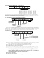
1
DM6910 User’s Manual RTD Embedded Technologies Inc. (Real Time Devices) Accessing the Analog World® BDM-610010015 Rev. A DM6910 User’s Manual RTD Embedded Technologies, INC. 103 Innovation Blvd. State College, PA 16803-0906 Phone: +1-814-234-8087 FAX: +1-814-234-5218 E-mail [email protected] [email protected] web site http://www.rtd.com Revision History Rev. A New manual naming method Published by: RTD Embedded Technologies, Inc. 103 Innovation Blvd. State College, PA 16803-0906 Copyright 1999, 2002, 2003 by RTD Embedded Technologies, Inc. All rights reserved Printed in U.S.A. The RTD Logo is a registered trademark of RTD Embedded Technologies. cpuModule and utilityModule are trademarks of RTD Embedded Technologies. PhoenixPICO and PheonixPICO BIOS are trademarks of Phoenix Technologies Ltd. PS/ 2, PC/XT, PC/AT and IBM are trademarks of International Business Machines Inc. MS-DOS, Windows, Windows 95, Windows 98 and Windows NT are trademarks of Microsoft Corp. PC/104 is a registered trademark of PC/104 Consortium. All other trademarks appearing in this document are the property of their respective owners. Table of Contents INTRODUCTION .................................................................................................................................... i-1 Digital I/O ............................................................................................................................................................... i-3 8254 Timer/Counters .............................................................................................................................................. i-3 What Comes With Your Module ............................................................................................................................ i-3 Module Accessories ................................................................................................................................................ i-3 Using This Manual .................................................................................................................................................. i-3 When You Need Help ............................................................................................................................................. i-3 CHAPTER 1 MODULE SETTINGS ............................................................................................... 1-1 Factory-Configured Switch and Jumper Settings .................................................................................................. 1-3 JP1, JP2 Interrupt Channel Select (Factory Setting: Jumper installed on G; IRQ Disabled) ..................... 1-4 JP3 8254 Clock and Gate Source Select (Factory Settings: See Figure 1-4) .............................................. 1-6 JP5 Strobe Input Enable (Factory Setting: Disabled) ................................................................................... 1-7 JP4 Interrupt Source Select (Factory Setting: OT2) .................................................................................... 1-7 SW1 Base Address (Factory Setting: 300 hex (768 decimal)) ..................................................................... 1-8 JP6 through JP11, Pull-up/Pull-down Resistors on Digital I/O Lines ................................................................... 1-9 CHAPTER 2 MODULE INSTALLATION .................................................................................... 2-1 Module Installation ................................................................................................................................................ 2-3 External I/O Connections ....................................................................................................................................... 2-3 Connecting the Digital I/O ................................................................................................................................. 2-4 Connecting the Timer/Counter I/O .................................................................................................................... 2-4 Connecting the External Interrupt ...................................................................................................................... 2-4 Running the 6910DIAG Diagnostics Program ...................................................................................................... 2-5 CHAPTER 3 HARDWARE DESCRIPTION ................................................................................. 3-1 Digital I/O .............................................................................................................................................................. 3-3 Timer/Counters ...................................................................................................................................................... 3-3 CHAPTER 4 I/O MAPPING ............................................................................................................ 4-1 Defining the I/O Map ............................................................................................................................................. 4-3 BA + 0: Digital I/O Port 0 (Read/Write) .......................................................................................................... 4-4 BA + 1: Digital I/O Port 1 (Read/Write) .......................................................................................................... 4-4 BA + 2: Clear IRQ/Program Port 0/Port 1 Direction/IRQ Source Registers (Read/Write) ............................. 4-4 BA + 3: Read Digital I/O Status/Program Digital Mode (Read/Write) ............................................................ 4-5 BA + 4: Digital I/O Port 2 (Read/Write) .......................................................................................................... 4-6 BA + 5: Digital I/O Port 3 (Read/Write) .......................................................................................................... 4-6 BA + 6: Clear IRQ/Program Port 0/Port 1 Direction/IRQ Source Registers (Read/Write) ............................. 4-6 BA + 7: Read Digital I/O Status/Program Digital Mode (Read/Write) ............................................................ 4-7 BA + 8: Digital I/O Port 4 (Read/Write) .......................................................................................................... 4-8 BA + 9: Digital I/O Port 5 (Read/Write) .......................................................................................................... 4-8 BA + 10: Clear IRQ/Program Port 0/Port 1 Direction/IRQ Source Registers (Read/Write) ........................... 4-8 BA + 11: Read Digital I/O Status/Program Digital Mode (Read/Write) ......................................................... 4-9 BA + 12: 8254 Timer/Counter 0 (Read/Write) ............................................................................................... 4-10 BA + 13: 8254 Timer/Counter 1 (Read/Write) ............................................................................................... 4-10 BA + 14: 8254 Timer/Counter 2 (Read/Write) .............................................................................................. 4-10 BA + 15: 8254 Timer/Counter Control Word (Write Only) .......................................................................... 4-10 i BA + 16: Clear IRQ/IRQ Enable (Read/Write) .............................................................................................. 4-10 BA + 17: IRQ Status (Read Only) .................................................................................................................. 4-11 BA + 18: Reserved .......................................................................................................................................... 4-11 BA + 19: Reserved .......................................................................................................................................... 4-11 Programming the DM6910 .................................................................................................................................. 4-12 Clearing and Setting Bits in a Port ....................................................................................................................... 4-12 CHAPTER 5 DIGITAL I/O ............................................................................................................. 5-1 Bit Programmable Digital I/O ................................................................................................................................ 5-3 Digital Interrupts .................................................................................................................................................... 5-3 Resetting the Digital Circuitry ............................................................................................................................... 5-3 Strobing Data into Ports 0/1, 2/3, and 4/5 .............................................................................................................. 5-3 CHAPTER 6 TIMER/COUNTERS ................................................................................................. 6-1 CHAPTER 7 INTERRUPTS ............................................................................................................ 7-1 JP4: Jumper Selectable Interrupts .......................................................................................................................... 7-3 Digital Interrupts .................................................................................................................................................... 7-3 Sampling Digital Lines for Change of State ...................................................................................................... 7-3 Selecting the Interrupt Channel .............................................................................................................................. 7-3 Interrupt Sharing .................................................................................................................................................... 7-3 Basic Programming For Interrupt Handling .......................................................................................................... 7-4 What Is an Interrupt? ......................................................................................................................................... 7-4 Interrupt Request Lines ...................................................................................................................................... 7-4 8259 Programmable Interrupt Controller .......................................................................................................... 7-4 Interrupt Mask Register (IMR) ...................................................................................................................... 7-4 End-of-Interrupt (EOI) Command ................................................................................................................. 7-4 What Exactly Happens When an Interrupt Occurs? .......................................................................................... 7-5 Using Interrupts in Your Programs .................................................................................................................... 7-5 Writing an Interrupt Service Routine (ISR) ....................................................................................................... 7-5 Saving the Startup Interrupt Mask Register (IMR) and Interrupt Vector ......................................................... 7-7 Restoring the Startup IMR and Interrupt Vector ............................................................................................... 7-7 Common Interrupt Mistakes .................................................................................................................................. 7-7 APPENDIX A DM6910 SPECIFICATIONS .................................................................................. A-1 APPENDIX B CONNECTOR PIN ASSIGNMENTS .................................................................... B-1 APPENDIX C COMPONENT DATA SHEETS ............................................................................ C-1 APPENDIX D WARRANTY ............................................................................................................ D-1 ii List of Illustrations 1-1 1-2 1-3 1-4 1-5 1-6 1-7 1-8 1-9 2-1 3-1 3-2 6-1 7-1 Module Layout Showing Factory-Configured Settings ........................................................................... 1-4 Interrupt Channel Select Jumpers, JP1 and JP2 ....................................................................................... 1-5 Pulling Down the Interrupt Request Lines ............................................................................................... 1-5 8254 Clock and Gate Sources Jumpers, JP3 ............................................................................................ 1-6 8254 Circuit Diagram ............................................................................................................................... 1-6 Strobe Input Enable Jumper, JP5 ............................................................................................................. 1-7 Interrupt Source Select Jumper, JP4 ........................................................................................................ 1-7 Base Address Switch, SW1 ...................................................................................................................... 1-8 Port 0 Pull-up/Pull-down Resistor Connections, JP6 ............................................................................... 1-9 CN3 I/O Connector Pin Assignments ...................................................................................................... 2-4 DM6910 Block Diagram .......................................................................................................................... 3-3 Timer/Counter Circuit Block Diagram ..................................................................................................... 3-4 8254 Timer/Counter Circuit Block Diagram ............................................................................................ 6-3 Digital Interrupt Timing Diagram ............................................................................................................ 7-3 iii iv INTRODUCTION i-1 i-2 The DM6910 digital I/O dataModule® turns your IBM PC-compatible cpuModule or other PC/104 computer into a high-performance control system. Ultra-compact for embedded and portable applications, the module features: 48 bit programmable digital I/O lines, Pull-up/pull-down resistors on each bit, Three 16-bit timer/counters and on-board 8 MHz clock, Operation from single +5V supply, DOS example programs with source code in BASIC and C, Diagnostics software. The following paragraphs briefly describe the major functions of the module. A detailed discussion of module functions is included in subsequent chapters. Digital I/O The DM6910 has 48 bit-programmable buffered TTL/CMOS digital I/O lines which are grouped into six 8-bit ports, Port 0 through Port 5. Three EPLD chips handle the digital I/O circuitry, with each EPLD carrying two ports, or 16 bit-programmable digital I/O lines. Bit configurable pull-up or pull-down resistors are provided for all 48 lines. Instructions for activating these pullup/pull-down resistors are given at the end of Chapter 1, Module Settings. 8254 Timer/Counters An 8254 programmable interval timer provides three 16-bit, 8 MHz timer/counters to support a wide range of user timing and counting functions. What Comes With Your Module You receive the following items in your module package: DM6910 interface module with stackthrough bus header Mounting hardware Example programs in BASIC and C with source code & diagnostics software Users manual If any item is missing or damaged, please call RTD Embedded Technologies Customer Service Department at (814) 234-8087. If you require service outside the U.S., contact your local distributor. Module Accessories Hardware accessories for the DM6910 include the XD68 cable and TB68 terminal block board. Using This Manual This manual is intended to help you install your new module and get it running quickly, while also providing enough detail about the module and its functions so that you can enjoy maximum use of its features even in the most complex applications. We assume that you already have an understanding of data acquisition principles and that you can customize the example software or write your own application programs. When You Need Help This manual and the example programs in the software package included with your module provide enough information to properly use all of the modules features. If you have any problems installing or using this dataModule, contact our Technical Support Department, (814) 234-8087, during regular business hours, eastern standard time or eastern daylight time, or send a FAX requesting assistance to (814) 234-5218. When sending a FAX request, please include your companys name and address, your name, your telephone number, and a brief description of the problem. You can also contact us through our E-mail address [email protected]. i-3 i-4 CHAPTER 1 MODULE SETTINGS The DM6910 has jumper and switch settings you can change if necessary for your application. The module is factory-configured as listed in the table and shown on the layout diagram in the beginning of this chapter. Should you need to change these settings, use these easyto-follow instructions before you stack the module with your computer system. Also note that by setting the jumpers as desired on header connectors JP6 through JP11, you can configure each digital I/O line to be pulled up or pulled down. This procedure is explained at the end of this chapter. 1-1 1-2 Factory-Configured Switch and Jumper Settings Table 1-1 lists the factory settings of the user-configurable jumpers and switch on the DM6910 module. Figure 1-1 shows the module layout and the locations of the factory-set jumpers. The following paragraphs explain how to change the factory settings. Pay special attention to the setting of SW1, the base address switch, to avoid address contention when you first use your module in your system. 7DEOH )DFWRU\ 6HWWLQJV 6ZLWFK )DFWRU\ 6HWWLQJV -XPSHU -XPSHUV ,QVWDOOHG )XQFWLRQ&RQWUROOHG &RQQHFWV D -3 MXPSHU VHOHFWDEOH RU GLJLWDO LQWHUUXSW -XPSHU LQVWDOOHG RQ * JURXQG -3 VRXUFH WR DQ LQWHUUXSW FKDQQHO SXOOV WULVWDWH EXIIHUV IRU EXIIHU LQWHUUXSW FKDQQHOV WR JURXQG * IRU PXOWLSOH LQWHUUXSW DSSOLFDWLRQV GLVDEOHG &RQQHFWV LQWHUUXSW VRXUFH MXPSHUHG RQ -3 WR DQ $7 -3 LQWHUUXSW FKDQQHO QR MXPSHU &/. 26& &/. 27 -3 6HWV WKH FORFN DQG JDWH VRXUFHV IRU WKH &/.27 *7(* WLPHUFRXQWHU WLPHUFRXQWHUV FDVFDGHG 6HOHFWV RQH RI IRXU LQWHUUXSW VRXUFHV IRU LQWHUUXSW -3 JHQHUDWLRQ 27 (QDEOHV DQG FRQQHFWV D VWUREH LQSXW WR 3RUW DQG RU WKURXJK WKH (;7 ,17 OLQH ',6 GLVDEOHG $FWLYDWHV SXOOXS SXOOGRZQ UHVLVWRUV RQ 3RUW $OO ELWV SXOOHG XS MXPSHUV GLJLWDO ,2 OLQHV LQVWDOOHG EHWZHHQ &20 9 $FWLYDWHV SXOOXS SXOOGRZQ UHVLVWRUV RQ 3RUW $OO ELWV SXOOHG XS MXPSHUV GLJLWDO ,2 OLQHV LQVWDOOHG EHWZHHQ &20 9 $FWLYDWHV SXOOXS SXOOGRZQ UHVLVWRUV RQ 3RUW $OO ELWV SXOOHG XS MXPSHUV GLJLWDO ,2 OLQHV LQVWDOOHG EHWZHHQ &20 9 $FWLYDWHV SXOOXS SXOOGRZQ UHVLVWRUV RQ 3RUW $OO ELWV SXOOHG XS MXPSHUV GLJLWDO ,2 OLQHV LQVWDOOHG EHWZHHQ &20 9 $FWLYDWHV SXOOXS SXOOGRZQ UHVLVWRUV RQ 3RUW $OO ELWV SXOOHG XS MXPSHUV GLJLWDO ,2 OLQHV LQVWDOOHG EHWZHHQ &20 9 $FWLYDWHV SXOOXS SXOOGRZQ UHVLVWRUV RQ 3RUW $OO ELWV SXOOHG XS MXPSHUV -3 GLJLWDO ,2 OLQHV LQVWDOOHG EHWZHHQ &20 9 6: 6HWVWKHEDVHDGGUHVV KH[ GHFLPDO -3 -3 -3 -3 -3 -3 1-3 Fig. 1-1 Module Layout Showing Factory-Configured Settings JP1, JP2 Interrupt Channel Select (Factory Setting: Jumper installed on G; IRQ Disabled) These header connectors, shown in Figure 1-2, lets you connect any one of four jumper selectable (JP4) interrupt sources and the Advanced Digital Interrupt sources to an interrupt channel, IRQ2 through IRQ15. XT channels 2 through 7 are jumpered on JP1 and AT channels 10 through 15 are jumpered on JP2. In AT computers channels 2 and 9 are the same channel. To activate a channel, you must install a jumper vertically across the desired IRQ channels pins. Only one channel on either JP1 or JP2 should be jumpered at any time. Figure 1-2a shows the factory settings. This module supports an interrupt sharing mode where the pins labeled G connect a 1 kilohm pull-down resistor to the output of a high-impedance tri-state driver which carries the interrupt request signal. This pull-down resistor drives the interrupt request line low whenever interrupts are not active. Whenever an interrupt request is made, the tri-state buffer is enabled, forcing the output high and generating an interrupt. There are four IRQ circuits, one for the P14 jumper selectable interrupts and one each for the digital interrupts available at Ports 0, 2, and 4. Their outputs are tied together through an "OR" gate, allowing all interrupt sources to share the same IRQ channel. To determine which circuit has generated an interrupt on the selected IRQ channel, read the status byte (I/O address location BA + 17) and check the status of bits 0 through 3, as described in Chapter 4. After the interrupt has been serviced, you must return the IRQ line low, disabling the tri-state buffer and pulling the output low again. This is done by clearing the IRQ for the source which generated the interrupt. You also can have two or more modules that share the same IRQ channel. You can tell which module issued the interrupt request by monitoring each modules IRQ status bit(s). If you are not planning on sharing interrupts or if you are not sure that your CPU supports interrupt sharing, it is best to disable this feature and use the interrupts in the normal mode. This will insure compatibility with all CPUs. See chapter 4 for details on disabling the interrupt sharing circuit. NOTE: When using multiple modules sharing the same interrupt, only one module should have the G jumper installed. The rest should be disconnected. Whenever you operate a single module, the G jumper should be installed. Whenever you operate the module with interrupt sharing disabled, the G jumper should be removed. 1-4 15 14 12 11 JP2 10 2 3 4 5 6 7 G JP1 Fig. 1-2 Interrupt Channel Select Jumpers, JP1 and JP2 PROGRAMMABLE INVERT JP4 INTERRUPT SOURCE JP4 IRQ STATUS (BA+17, BIT 3) CLK INTERRUPT REGISTER +5 V INTERRUPT CLR CLR PORT 0, 1 DIGITAL INTERRUPT JP1 G PORT 0, 1 DIGITAL IRQ STATUS (BA+17, BIT 0) CLK INTERRUPT REGISTER CLR CLR PORT 2, 3 DIGITAL INTERRUPT PORT 2, 3 DIGITAL IRQ STATUS (BA+17, BIT 1) CLK INTERRUPT REGISTER CLR CLR PORT 4, 5 DIGITAL INTERRUPT PORT 4, 5 DIGITAL IRQ STATUS (BA+17, BIT 2) CLK INTERRUPT REGISTER CLR CLR Fig. 1-3 Pulling Down the Interrupt Request Lines 1-5 JP3 8254 Clock and Gate Source Select (Factory Settings: See Figure 1-4) This header connector, shown in Figure 1-4, lets you select the clock sources for the three 8254 16-bit timer/ counters. Figure 1-5 shows a block diagram of the timer/counter circuitry to help you in making these connections. The clock source for Counter 0 is selected by placing a jumper on one of the two leftmost pairs of pins on the header, OSC or EC0. OSC is the on-board 8 MHz clock, and EC0 is an external clock source which can be connected through I/O connector CN3, pin 55. Counter 1 has three clock sources: OT0, which cascades it to Counter 0; OSC, which is the on-board 8 MHz clock; and EC1, which is an external clock source connected through I/O connector CN3, pin 59. Counter 2 has three clock sources: OT1, which cascades it to Counter 1; OSC, which is the on-board 8 MHz clock; and EC2, which is an external clock source connected through I/O connector CN3, pin 61. The gate of Counter 2 can be connected to the output of Counter 1 (OT1) or to an external gate source (EG2) connected through I/O connector CN3, pin 62. When no external gate source is connected, this line is tied high. JP3 CLK0 OSC EC0 CLK1 OT0 OSC EC1 CLK2 OT1 OSC EC2 GT2 OT1 EG2 Fig. 1-4 8254 Clock and Gate Sources Jumpers, JP3 ON-BOARD I/O CONNECTOR CN3 8254 JP3 CLK0 TIMER/ COUNTER 0 XTAL (8 MHz) PIN 55 CLK +5 V GATE OUT OUT0 TIMER/ COUNTER 1 EXT CLK 0 PIN 56 EXT GATE 0 PIN 57 T/C OUT 0 PIN 59 EXT CLK 1 PIN 60 EXT GATE 1 PIN 58 T/C OUT 1 PIN 61 EXT CLK 2 PIN 62 EXT GATE 2 PIN 63 T/C OUT 2 CLK1 CLK +5 V GATE OUT CLK2 OUT1 TIMER/ COUNTER 2 CLK +5 V GATE OUT Fig. 1-5 8254 Circuit Diagram 1-6 JP5 Strobe Input Enable (Factory Setting: Disabled) DIS P4 P2 P0 DIS P4 P2 P0 This header connector, shown in Figure 1-6, connects an external signal (through CN3-64, EXT INT1) to the strobe input of Port 0, Port 2, and/or Port 4. To enable the strobe input on the digital I/O chip of a selected port, you must remove the jumper from the DIS (disable) pins and place it across the desired port. Note that multiple ports can be strobed from the same signal. JP5 JP5 Fig. 1-6b: Port 0 Strobe Enabled Fig. 1-6a: Strobe Disabled (Factory Setting) Fig. 1-6 Strobe Input Enable Jumper, JP5 JP4 Interrupt Source Select (Factory Setting: OT2) OT2 OT1 EI1 EI2 This header connector, shown in Figure 1-7, lets you select one of four interrupt sources for interrupt generation. These sources are not part of the EPLD digital interrupt circuitry. The four sources are: EI1, external interrupt 1, CN364; EI2, external interrupt 2, CN3-54; OT1, the output of timer/counter 1; and OT2, the output of timer/counter 2. To connect an interrupt source, place the jumper across the desired set of pins. JP4 Fig. 1-7 Interrupt Source Select Jumper, JP4 1-7 SW1 Base Address (Factory Setting: 300 hex (768 decimal)) One of the most common causes of failure when you are first trying your module is address contention. Some of your computers I/O space is already occupied by internal I/O and other peripherals. When the module attempts to use I/O address locations already used by another device, contention results and the board does not work. To avoid this problem, the DM6910 has an easily accessible DIP switch, SW1, which lets you select any one of 16 starting addresses in the computers I/O. Should the factory setting of 300 hex (768 decimal) be unsuitable for your system, you can select a different base address simply by setting the switches to any one of the values listed in Table 1-2. The table shows the switch settings and their corresponding decimal and hexadecimal (in parentheses) values. Make sure that you verify the order of the switch numbers on the switch (1 through 4) before setting them. When the switches are pulled forward, they are OPEN, or set to logic 1, as labeled on the DIP switch package. When you set the base address for your module, record the value in the table inside the back cover. Figure 1-8 shows the DIP switch set for a base address of 300 hex (768 decimal). 7DEOH %DVH $GGUHVV 6ZLWFK 6HWWLQJV 6: %DVH $GGUHVV 6ZLWFK 6HWWLQJ %DVH $GGUHVV 6ZLWFK 6HWWLQJ 'HFLPDO +H[ 'HFLPDO +H[ $ $ & & ( ( FORVHG RSHQ Fig. 1-8 Base Address Switch, SW1 1-8 JP6 through JP11, Pull-up/Pull-down Resistors on Digital I/O Lines The DM6910 has 48 TTL/CMOS compatible digital I/O lines which can be interfaced with external devices. These lines are divided into six ports, Port 0 through Port 5,with eight bit programmable lines per port. You can connect pull-up or pull-down resistors to any or all of these lines on a bit by bit basis. You may want to pull lines up for connection to switches. This will pull the line high when the switch is disconnected. Or, you may want to pull lines down for connection to relays which control turning motors on and off. These motors turn on when the digital lines controlling them are high. By pulling these lines down, you can ensure that when the data acquisition system is first turned on, the motors will not switch on before the port is initialized. Pull-up/pull-down resistors have been factory installed on the module, and jumpers have been installed in the pull-up position on JP6 through JP11 for all 48 I/O lines. Each port and bit is labeled on the module. JP6 connects to the resistors for Port 0, JP7 connects to the resistors for Port 1, and so on. The pins are labeled G (for ground) on one end and V (for +5V) on the other end. The middle pin is common. Figure 1-9 shows JP6 with the factory-installed jumpers placed between the common pin (middle pin of the three) and the V pin. For pull-downs, install the jumper across the common pin (middle pin) and G pin. To disable the pull-up/pull-down resistor, remove the jumper. G V JP6 0 1 PORT 0 2 3 4 5 6 7 Fig. 1-9 Port 0 Pull-up/Pull-down Resistor Connections, JP6 1-9 1-10 CHAPTER 2 MODULE INSTALLATION The DM6910 is easy to install in your cpuModule or other PC/104 based system. This chapter tells you step-by-step how to install and connect the module. After you have installed the module and made all of your connections, you can turn your system on and run the 6910DIAG board diagnostics program included on your example software disk to verify that your module is working. 2-1 2-2 Module Installation Keep the module in its antistatic bag until you are ready to install it in your cpuModule or other PC/104 based system. When removing it from the bag, hold the module at the edges and do not touch the components or connectors. Before installing the module in your system, check the jumper and switch settings. Chapter 1 reviews the factory settings and how to change them. If you need to change any settings, refer to the appropriate instructions in Chapter 1. Note that incompatible jumper settings can result in unpredictable module operation and erratic response. The DM6910 comes with a stackthrough bus connector. The stackthrough connector lets you stack another module on top of your DM6910. To install the module, follow the procedures described in the computer manual and the steps below: 1. Turn OFF the power to your system. 2. Touch a metal rack to discharge any static buildup and then remove the module from its antistatic bag. 3. Select the appropriate standoffs for your application to secure the module when you install it in your system (two sizes are included with the module). 4. Holding the module by its edges, orient it so that the CN1 bus connectors pin 1 lines up with pin 1 of the expansion connector onto which you are installing the module. 5. After carefully positioning the module so that the pins are lined up and resting on the expansion connector, gently and evenly press down on the module until it is secured on the connector. NOTE: Do not force the module onto the connector. If the module does not readily press into place, remove it and try again. Wiggling the module or exerting too much pressure can result in damage to the DM6910 or to the mating module. 6. After the module is installed, connect the cable to I/O connector CN3 on the module. 7. Make sure all connections are secure. External I/O Connections Figure 2-1 shows I/O connector pinout for CN3. Refer to this diagram as you make your I/O connections. 2-3 P4.7 1 2 P5.7 P4.6 3 4 P5.6 P4.5 5 6 P5.5 P4.4 7 8 P5.4 P4.3 9 10 P5.3 P4.2 11 12 P5.2 P4.1 13 14 P5.1 P4.0 15 16 P5.0 DIGITAL GND 17 18 DIGITAL GND P2.7 19 20 P3.7 P2.6 21 22 P3.6 P2.5 23 24 P3.5 P2.4 25 26 P3.4 P2.3 27 28 P3.3 P2.2 29 30 P3.2 P2.1 31 32 P3.1 P2.0 33 34 P3.0 DIGITAL GND 35 36 DIGITAL GND P0.7 37 38 P1.7 P0.6 39 40 P1.6 P0.5 41 42 P1.5 P0.4 43 44 P1.4 P0.3 45 46 P1.3 P0.2 47 48 P1.2 P0.1 49 50 P1.1 P0.0 51 52 P1.0 DIGITAL GND 53 54 EXT INT 2 EXT CLK 0 55 56 EXT GATE 0 T/C OUT 0 57 58 T/C OUT 1 EXT CLK 1 59 60 EXT GATE 1 EXT CLK 2 61 62 EXT GATE 2 T/C OUT 2 63 64 EXT INT 1 +5 VOLTS 65 66 DIGITAL GND +5 VOLTS 67 68 DIGITAL GND Fig. 2-1 CN3 I/O Connector Pin Assignment Connecting the Digital I/O For all digital I/O connections, the high side of an external signal source or destination device is connected to the appropriate signal pin on the I/O connector, and the low side is connected to the DIGITAL GND. Connecting the Timer/Counter I/O External connections to the timer/counters on the DM6910 can be made by connecting the high side of the external device to the appropriate signal pin on I/O connector CN3 and the low side to a DIGITAL GND. Connecting the External Interrupt The DM6910 can receive externally generated interrupt signals EXT INT1, through I/O connector CN3, pin 64, and EXT INT2, through I/O connector CN3, pin 54 and route them to an IRQ channel through on-board header connectors JP4, JP1 and JP2. Interrupt generation is enabled through software. When interrupts are enabled, a rising or falling edge on the EXT INT line will cause the selected IRQ line to go high, depending on the setting of BA + 16, bit 1, and the IRQ status bit will change from 0 to 1. The pulse applied to the EXT INT pin should have a duration of at least 100 nanoseconds. 2-4 Running the 6910DIAG Diagnostics Program Now that your module is ready to use, you will want to try it out. An easy-to-use, menu-driven diagnostics program, 6910DIAG, is included with your example software to help you verify your modules operation. You can also use this program to make sure that your current base address setting does not contend with another device. 2-5 2-6 CHAPTER 3 HARDWARE DESCRIPTION This chapter describes the features of the DM6910 hardware. The major circuits are the digital I/O lines and the timer/counters. 3-1 3-2 The DM6910 has two major circuits, the digital I/O lines and the timer/counters. Figure 3-1 shows the block diagram of the module. This chapter describes the hardware which makes up the major circuits. 8 MHz OSC 8254 PIT ADDRESS 9 ADDRESS DECODE 3 I/O CONNECTOR INTERRUPT CONTROL PC BUS 3 X 8-BIT BYTE PROGRAMMABLE DIGITAL I/O EVENT/MATCH CONTROL DATA 8 3 X 8-BIT BIT PROGRAMMABLE DIGITAL I/O 24 +5 VOLTS CONTROL Fig. 3-1 DM6910 Block Diagram Digital I/O The 48 bit-programmable digital I/O lines can be used to transfer data between the computer and external devices. Six ports, Ports 0, 1, 2, 3, 4, and 5, each provide eight bit programmable lines which can be independently set for input or output. The digital I/O circuitry is contained in three EPLD chips on the module 16 lines per chip grouped as follows: Port 0/1 EPLD, Port 2/3 EPLD, and Port 4/5 EPLD. One line per chip can be used to generate a digital interrupt. Chapter 5 details digital I/O operations and Chapter 7 explains digital interrupts. Timer/Counters An 8254 programmable interval timer provides three 16-bit, 8-MHz timer/counters to support a wide range of timing and counting functions. Figure 3-2 shows the timer/counter circuitry. Each 16-bit timer/counter has two inputs, CLK in and GATE in, and one output, timer/counter OUT. Each can be programmed as binary or BCD down counters by writing the appropriate data to the command word, as described in Chapter 4. The command word also lets you set up the mode of operation. The six programmable modes are: 3-3 Mode 0 Mode 1 Mode 2 Mode 3 Mode 4 Mode 5 Event Counter (Interrupt on Terminal Count) Hardware-Retriggerable One-Shot Rate Generator Square Wave Mode Software-Triggered Strobe Hardware Triggered Strobe (Retriggerable) These modes are detailed in the 8254 Data Sheet, reprinted from Intel in Appendix C. ON-BOARD I/O CONNECTOR CN3 8254 JP3 CLK0 TIMER/ COUNTER 0 XTAL (8 MHz) CLK +5 V GATE OUT OUT0 TIMER/ COUNTER 1 PIN 55 EXT CLK 0 PIN 56 EXT GATE 0 PIN 57 T/C OUT 0 PIN 59 EXT CLK 1 PIN 60 EXT GATE 1 PIN 58 T/C OUT 1 PIN 61 EXT CLK 2 PIN 62 EXT GATE 2 PIN 63 T/C OUT 2 CLK1 CLK +5 V GATE OUT CLK2 OUT1 TIMER/ COUNTER 2 CLK +5 V GATE OUT Fig. 3-2 Timer/Counter Circuit Block Diagram 3-4 CHAPTER 4 I/O MAPPING This chapter provides a complete description of the I/O map for the DM6910, general programming information, and how to set and clear bits in a port. 4-1 4-2 Defining the I/O Map The I/O map for the DM6910 is shown in Table 4-1 below. As shown, the board occupies 20 consecutive I/O port locations. To conserve the use of I/O space, the structure of the I/O map is such that some of the registers control what operation you are performing at other addresses. The digital registers you address at BA + 2, 6, and 10 are selected at BA + 3, 7, and 11. This scheme is easily understood once you review the register descriptions on the following pages. The base address (designated as BA) can be selected using DIP switch SW1, located on the edge of the module, as described in Chapter 1, Module Settings. This switch can be accessed without removing the module from the stack. The following sections describe the register contents of each address used in the I/O map. 7DEOH'0,20DS $GGUHVV 5HJLVWHU'HVFULSWLRQ 5HDG)XQFWLRQ :ULWH)XQFWLRQ 'HFLPDO 'LJLWDO,23RUW 5HDG3RUWGLJLWDOLQSXWOLQHV 3URJUDP3RUWGLJLWDORXWSXWOLQHV %$ 'LJLWDO,23RUW 5HDG3RUWGLJLWDOLQSXWOLQHV 3URJUDP3RUWGLJLWDORXWSXWOLQHV %$ &OHDUGLJLWDO,54VWDWXVIODJUHDG &OHDUGLJLWDOFKLSSURJUDP3RUW &OHDU,543URJUDP3RUW 3RUWGLUHFWLRQ3RUWGLUHFWLRQRU GLUHFWLRQ3RUWGLUHFWLRQRU,54 'LUHFWLRQ,546RXUFH ,54VRXUFHGHSHQGHQWRQ%$ VRXUFHGHSHQGHQWRQ%$ %$ 5HJLVWHU 5HDGGLJLWDOLQWHUUXSWVWDWXVZRUG 3URJUDPGLJLWDOFRQWUROUHJLVWHU %$ 'LJLWDO,23RUW 5HDG3RUWGLJLWDOLQSXWOLQHV 3URJUDP3RUWGLJLWDORXWSXWOLQHV %$ 'LJLWDO,23RUW 5HDG3RUWGLJLWDOLQSXWOLQHV 3URJUDP3RUWGLJLWDORXWSXWOLQHV %$ &OHDUGLJLWDO,54VWDWXVIODJUHDG &OHDUGLJLWDOFKLSSURJUDP3RUW &OHDU,543URJUDP3RUW 3RUWGLUHFWLRQ3RUWGLUHFWLRQRU GLUHFWLRQ3RUWGLUHFWLRQRU,54 'LUHFWLRQ,546RXUFH ,54VRXUFHGHSHQGHQWRQ%$ VRXUFHGHSHQGHQWRQ%$ %$ 5HJLVWHU 5HDGGLJLWDOLQWHUUXSWVWDWXVZRUG 3URJUDPGLJLWDOFRQWUROUHJLVWHU %$ 'LJLWDO,23RUW 5HDG3RUWGLJLWDOLQSXWOLQHV 3URJUDP3RUWGLJLWDORXWSXWOLQHV %$ 'LJLWDO,23RUW 5HDG3RUWGLJLWDOLQSXWOLQHV 3URJUDP3RUWGLJLWDORXWSXWOLQHV %$ 5HDG'LJLWDO,546WDWXV 6HW'LJLWDO&RQWURO 5HDG'LJLWDO,546WDWXV 6HW'LJLWDO&RQWURO &OHDUGLJLWDO,54VWDWXVIODJUHDG 3RUWGLUHFWLRQ3RUWGLUHFWLRQRU &OHDUGLJLWDOFKLSSURJUDP3RUW &OHDU,543URJUDP3RUW ,54VRXUFHGHSHQGHQWRQ%$ GLUHFWLRQ3RUWGLUHFWLRQRU,54 'LUHFWLRQ,546RXUFH VRXUFHGHSHQGHQWRQ%$ %$ 5HJLVWHU 5HDGGLJLWDOLQWHUUXSWVWDWXVZRUG 3URJUDPGLJLWDOFRQWUROUHJLVWHU %$ 7&&RXQWHU 5HDGYDOXHLQ&RXQWHU /RDGFRXQWLQ&RXQWHU %$ 7&&RXQWHU 5HDGYDOXHLQ&RXQWHU /RDGFRXQWLQ&RXQWHU %$ 7&&RXQWHU 5HDGYDOXHLQ&RXQWHU /RDGFRXQWLQ&RXQWHU %$ &RQWURO:RUG 5HVHUYHG 3URJUDPFRXQWHUPRGH %$ 5HDG'LJLWDO,546WDWXV 6HW'LJLWDO&RQWURO (QDEOHLQWHUUXSWOLQH-3 &OHDU,54,54(QDEOH &OHDULQWHUUXSWOLQH-3 'LVDEOHLQWHUUXSWVKDULQJ %$ ,546WDWXV 5HDGLQWHUUXSWVWDWXV 5HVHUYHG %$ 5HVHUYHG 5HVHUYHG 5HVHUYHG %$ 5HVHUYHG 5HVHUYHG 5HVHUYHG %$ %$ %DVH$GGUHVV 4-3 BA + 0: Digital I/O Port 0 (Read/Write) This port transfers the 8-bit Port 0 bit programmable digital input/output data between the module and external devices. The bits are individually programmed as input or output by writing to the Port 0 Direction Register at BA + 2. For all bits set as inputs, a read reads the input values and a write is ignored. For all bits set as outputs, a read reads the last value sent out on the line and a write writes the current loaded value out to the line. Note that when any reset of the digital circuitry is performed (clear chip or computer reset), all digital lines are reset to inputs and their corresponding output registers are cleared. D7 D6 D5 D4 D3 D2 D1 D0 P0.7 P0.6 P0.5 P0.4 P0.3 P0.2 P0.1 P0.0 BA + 1: Digital I/O Port 1 (Read/Write) This port transfers the 8-bit Port 1 bit programmable digital input/output data between the module and external devices. The bits are individually programmed as input or output by writing to the Port 1 Direction Register at BA + 2. For all bits set as inputs, a read reads the input values and a write is ignored. For all bits set as outputs, a read reads the last value sent out on the line and a write writes the current loaded value out to the line. Note that when any reset of the digital circuitry is performed (clear chip or computer reset ), all digital lines are reset to inputs and their corresponding output registers are cleared. D7 D6 D5 D4 D3 D2 D1 D0 P1.7 P1.6 P1.5 P1.4 P1.3 P1.2 P1.1 P1.0 BA + 2: Clear IRQ/Program Port 0 Direction/Port 1 Direction/IRQ Source Registers (Read/Write) A read clears the IRQ status flag or provides the contents of one of three control registers: Port 0 Direction, Port 1 Direction, or Port 0/1 EPLD IRQ Source. A write clears the digital chip or programs one of the three control registers, depending on the setting of bits 0 and 1 at BA + 3. When bits 1 and 0 at BA + 3 are 00, the read/write operations clear the digital IRQ status flag (read) and the digital chip (write). When these bits are set to any other value, one of the three Port 0/1 digital I/O registers is addressed. Port 0 Direction Register (BA + 3, bits 1 and 0 = 01): For all bits: 0 = input 1 = output D7 D6 D5 D4 D3 D2 D1 D0 P0.7 P0.6 P0.5 P0.4 P0.3 P0.2 P0.1 P0.0 This register programs the direction, input or output, of each bit at Port 0. Port 1 Direction Register (BA + 3, bits 1 and 0 = 10): For all bits: 0 = input 1 = output D7 D6 D5 D4 D3 D2 D1 D0 P1.7 P1.6 P1.5 P1.4 P1.3 P1.2 This register programs the direction, input or output, of each bit at Port 1. 4-4 P1.1 P1.0 Port 0/1 EPLD IRQ Source Register (BA + 3, bits 1 and 0 = 11): D7 D6 D5 D4 D3 D2 D1 D0 Port 0/1 IRQ Select 0000 = P0.0 0100 = P0.4 0001 = P0.1 0101 = P0.5 0010 = P0.2 0110 = P0.6 0011 = P0.3 0111 = P0.7 1000 = P1.0 1001 = P1.1 1010 = P1.2 1011 = P1.3 1100 = P1.4 1101 = P1.5 1110 = P1.6 1111 = P1.7 This register programs the bit to be used to generate a digital interrupt for the Port 0/1 EPLD. A digital interrupt is generated when the selected bit goes from low to high or high to low depending on the IRQ Polarity bit below. If the Strobe input is enabled, the strobe signal will generate the interrupt. BA + 3: Read Digital I/O Status/Program Digital Mode (Read/Write) D7 D6 D5 D4 D3 D2 D1 D0 Digital IRQ Status 0 = no digital interrupt 1 = digital interrupt IRQ Polarity Strobe Enable BA + 2 Register Select Strobe Status Digital IRQ Enable 0 = no strobe Digital Sample 1 = strobe Clock Select A read shows you whether a digital interrupt or a strobe has occurred and lets you review the states of the other bits in this register. If bit 6 is high, then an input strobe has taken place. This bit will be reset when the data is read. If bit 7 is high, then a digital interrupt has taken place. This provides the same status information as BA + 17, bit 0. Digital Mode Register: D7 D6 D5 D4 D3 D2 D1 D0 Reserved Reserved Digital Sample Clock Select 0 = 8 MHz system clock 1 = programmable clock Digital IRQ Enable 0 = disabled 1 = enabled IRQ Polarity 0 = rising edge 1 = falling edge BA + 2 Register Select 00 = clear mode 01 = Port 0 Direction Register 10 = Port 1 Direction Register 11 = IRQ Source Register Strobe Enable 0 = disabled 1 = enabled Bits 0 and 1 Select the clear mode initiated by a read/write operation at BA + 2 or the control register you talk to at BA + 2 (Port 0 Direction, Port 1 Direction, or Port 0/1 EPLD IRQ Select Register). Bit 2 IRQ Polarity sets the edge of the digital input signal that generates the interrupt . Bit 3 Enables EPLD strobe input (used with JP5 header). Bit 4 Disables/enables digital interrupts. The IRQ channel is determined by the jumper setting on JP1 and JP2. Bit 5 Sets the clock rate at which the digital lines are sampled when in a digital interrupt mode. Available clock sources are the 8 MHz system clock and the output of the 8254 Counter 1 (16-bit programmable clock). When a digital input line changes state, it must stay at the new state for two edges of the clock pulse (62.5 nanoseconds when using the 8 MHz clock) before it is recognized and before an interrupt can be generated. This feature eliminates noise glitches that can cause a false state change on an input line and generate an unwanted interrupt. This feature is detailed in Chapter 5. Bit 6 Read only (Strobe status). Bit 7 Read only (digital IRQ status). 4-5 BA + 4: Digital I/O Port 2 (Read/Write) This port transfers the 8-bit Port 2 bit programmable digital input/output data between the module and external devices. The bits are individually programmed as input or output by writing to the Port 2 Direction Register at BA + 6. For all bits set as inputs, a read reads the input values and a write is ignored. For all bits set as outputs, a read reads the last value sent out on the line and a write writes the current loaded value out to the line. Note that when any reset of the digital circuitry is performed (clear chip or computer reset), all digital lines are reset to inputs and their corresponding output registers are cleared. D7 D6 D5 D4 D3 D2 D1 D0 P2.7 P2.6 P2.5 P2.4 P2.3 P2.2 P2.1 P2.0 BA + 5: Digital I/O Port 3 (Read/Write) This port transfers the 8-bit Port 3 bit programmable digital input/output data between the module and external devices. The bits are individually programmed as input or output by writing to the Port 3 Direction Register at BA + 6. For all bits set as inputs, a read reads the input values and a write is ignored. For all bits set as outputs, a read reads the last value sent out on the line and a write writes the current loaded value out to the line. Note that when any reset of the digital circuitry is performed (clear chip or computer reset ), all digital lines are reset to inputs and their corresponding output registers are cleared. D7 D6 D5 D4 D3 D2 D1 D0 P3.7 P3.6 P3.5 P3.4 P3.3 P3.2 P3.1 P3.0 BA + 6: Clear IRQ/Program Port 2 Direction/Port 3 Direction/IRQ Source Registers (Read/Write) A read clears the IRQ status flag or provides the contents of one of three control registers: Port 2 Direction, Port 3 Direction, or Port 2/3 EPLD IRQ Source. A write clears the digital chip or programs one of the three control registers, depending on the setting of bits 0 and 1 at BA + 7. When bits 1 and 0 at BA + 7 are 00, the read/write operations clear the digital IRQ status flag (read) and the digital chip (write). When these bits are set to any other value, one of the three Port 2/3 digital I/O registers is addressed. Port 2 Direction Register (BA + 7, bits 1 and 0 = 01): For all bits: 0 = input 1 = output D7 D6 D5 D4 D3 D2 D1 D0 P2.7 P2.6 P2.5 P2.4 P2.3 P2.2 P2.1 P2.0 This register programs the direction, input or output, of each bit at Port 2. Port 3 Direction Register (BA + 7, bits 1 and 0 = 10): For all bits: 0 = input 1 = output D7 D6 D5 D4 D3 D2 D1 D0 P3.7 P3.6 P3.5 P3.4 P3.3 P3.2 This register programs the direction, input or output, of each bit at Port 3. 4-6 P3.1 P3.0 Port 2/3 EPLD IRQ Source Register (BA + 7, bits 1 and 0 = 11): D7 D6 D5 D4 D3 D2 D1 D0 Port 2/3 IRQ Select 0000 = P2.0 0100 = P2.4 0001 = P2.1 0101 = P2.5 0010 = P2.2 0110 = P2.6 0011 = P2.3 0111 = P2.7 1000 = P3.0 1001 = P3.1 1010 = P3.2 1011 = P3.3 1100 = P3.4 1101 = P3.5 1110 = P3.6 1111 = P3.7 This register programs the bit to be used to generate a digital interrupt for the Port 2/3 EPLD. A digital interrupt is generated when the selected bit goes from low to high or high to low depending on the IRQ Polarity bit below. If the Strobe input is enabled, the strobe signal will generate the interrupt. BA + 7: Read Digital I/O Status/Program Digital Mode (Read/Write) D7 D6 D5 D4 D3 D2 D1 D0 Digital IRQ Status 0 = no digital interrupt 1 = digital interrupt IRQ Polarity Strobe Enable BA + 6 Register Select Strobe Status Digital IRQ Enable 0 = no strobe Digital Sample 1 = strobe Clock Select A read shows you whether a digital interrupt or a strobe has occurred and lets you review the states of the other bits in this register. If bit 6 is high, then an input strobe has taken place. This bit will be reset when the data is read. If bit 7 is high, then a digital interrupt has taken place. This provides the same status information as BA + 17, bit 0. Digital Mode Register: D7 D6 D5 D4 D3 D2 D1 D0 Reserved Reserved Digital Sample Clock Select 0 = 8 MHz system clock 1 = programmable clock Digital IRQ Enable 0 = disabled 1 = enabled IRQ Polarity 0 = rising edge 1 = falling edge BA + 6 Register Select 00 = clear mode 01 = Port 2 Direction Register 10 = Port 3 Direction Register 11 = IRQ Source Register Strobe Enable 0 = disabled 1 = enabled Bits 0 and 1 Select the clear mode initiated by a read/write operation at BA + 6 or the control register you talk to at BA + 6 (Port 2 Direction, Port 3 Direction, or Port 2/3 EPLD IRQ Select Register). Bit 2 IRQ Polarity sets the edge of the digital input signal that generates the interrupt . Bit 3 Enables EPLD strobe input (used with JP5 header). Bit 4 Disables/enables digital interrupts. The IRQ channel is determined by the jumper setting on JP1 and JP2. Bit 5 Sets the clock rate at which the digital lines are sampled when in a digital interrupt mode. Available clock sources are the 8 MHz system clock and the output of the 8254 Counter 1 (16-bit programmable clock). When a digital input line changes state, it must stay at the new state for two edges of the clock pulse (62.5 nanoseconds when using the 8 MHz clock) before it is recognized and before an interrupt can be generated. This feature eliminates noise glitches that can cause a false state change on an input line and generate an unwanted interrupt. This feature is detailed in Chapter 5. Bit 6 Read only (Strobe status). Bit 7 Read only (digital IRQ status). 4-7 BA + 8: Digital I/O Port 4 (Read/Write) This port transfers the 8-bit Port 4 bit programmable digital input/output data between the module and external devices. The bits are individually programmed as input or output by writing to the Port 4 Direction Register at BA + 10. For all bits set as inputs, a read reads the input values and a write is ignored. For all bits set as outputs, a read reads the last value sent out on the line and a write writes the current loaded value out to the line. Note that when any reset of the digital circuitry is performed (clear chip or computer reset), all digital lines are reset to inputs and their corresponding output registers are cleared. D7 D6 D5 D4 D3 D2 D1 D0 P4.7 P4.6 P4.5 P4.4 P4.3 P4.2 P4.1 P4.0 BA + 9: Digital I/O Port 5 (Read/Write) This port transfers the 8-bit Port 5 bit programmable digital input/output data between the module and external devices. The bits are individually programmed as input or output by writing to the Port 5 Direction Register at BA + 10. For all bits set as inputs, a read reads the input values and a write is ignored. For all bits set as outputs, a read reads the last value sent out on the line and a write writes the current loaded value out to the line. Note that when any reset of the digital circuitry is performed (clear chip or computer reset ), all digital lines are reset to inputs and their corresponding output registers are cleared. D7 D6 D5 D4 D3 D2 D1 D0 P5.7 P5.6 P5.5 P5.4 P5.3 P5.2 P5.1 P5.0 BA + 10: Clear IRQ/Program Port 4 Direction/Port 5 Direction/IRQ Source Registers (Read/Write) A read clears the IRQ status flag or provides the contents of one of three control registers: Port 4 Direction, Port 5 Direction, or Port 4/5 EPLD IRQ Source. A write clears the digital chip or programs one of the three control registers, depending on the setting of bits 0 and 1 at BA + 11. When bits 1 and 0 at BA + 11 are 00, the read/write operations clear the digital IRQ status flag (read) and the digital chip (write). When these bits are set to any other value, one of the three Port 4/5 digital I/O registers is addressed. Port 4 Direction Register (BA + 11, bits 1 and 0 = 01): For all bits: 0 = input 1 = output D7 D6 D5 D4 D3 D2 D1 D0 P4.7 P4.6 P4.5 P4.4 P4.3 P4.2 P4.1 P4.0 This register programs the direction, input or output, of each bit at Port 4. Port 5 Direction Register (BA + 11, bits 1 and 0 = 10): For all bits: 0 = input 1 = output D7 D6 D5 D4 D3 D2 D1 D0 P5.7 P5.6 P5.5 P5.4 P5.3 P5.2 This register programs the direction, input or output, of each bit at Port 5. 4-8 P5.1 P5.0 Port 4/5 EPLD IRQ Source Register (BA + 11, bits 1 and 0 = 11): D7 D6 D5 D4 D3 D2 D1 D0 Port 4/5 IRQ Select 0000 = P4.0 0100 = P4.4 0001 = P4.1 0101 = P4.5 0010 = P4.2 0110 = P4.6 0011 = P4.3 0111 = P4.7 1000 = P5.0 1001 = P5.1 1010 = P5.2 1011 = P5.3 1100 = P5.4 1101 = P5.5 1110 = P5.6 1111 = P5.7 This register programs the bit to be used to generate a digital interrupt for the Port 4/5 EPLD. A digital interrupt is generated when the selected bit goes from low to high or high to low depending on the IRQ Polarity bit below. If the Strobe input is enabled, the strobe signal will generate the interrupt. BA + 11: Read Digital I/O Status/Program Digital Mode (Read/Write) D7 D6 D5 D4 D3 D2 D1 D0 Digital IRQ Status 0 = no digital interrupt 1 = digital interrupt IRQ Polarity Strobe Enable BA + 10 Register Select Strobe Status Digital IRQ Enable 0 = no strobe Digital Sample 1 = strobe Clock Select A read shows you whether a digital interrupt or a strobe has occurred and lets you review the states of the other bits in this register. If bit 6 is high, then an input strobe has taken place. This bit will be reset when the data is read. If bit 7 is high, then a digital interrupt has taken place. This provides the same status information as BA + 17, bit 0. Digital Mode Register: D7 D6 D5 D4 D3 D2 D1 D0 Reserved Reserved Digital Sample Clock Select 0 = 8 MHz system clock 1 = programmable clock Digital IRQ Enable 0 = disabled 1 = enabled IRQ Polarity 0 = rising edge 1 = falling edge BA + 10 Register Select 00 = clear mode 01 = Port 4 Direction Register 10 = Port 5 Direction Register 11 = IRQ Source Register Strobe Enable 0 = disabled 1 = enabled Bits 0 and 1 Select the clear mode initiated by a read/write operation at BA + 10 or the control register you talk to at BA + 10 (Port 4 Direction, Port 5 Direction, or Port 4/5 EPLD IRQ Select Register). Bit 2 IRQ Polarity sets the edge of the digital input signal that generates the interrupt . Bit 3 Enables EPLD strobe input (used with JP5 header). Bit 4 Disables/enables digital interrupts. The IRQ channel is determined by the jumper setting on JP1 and JP2. Bit 5 Sets the clock rate at which the digital lines are sampled when in a digital interrupt mode. Available clock sources are the 8 MHz system clock and the output of the 8254 Counter 1 (16-bit programmable clock). When a digital input line changes state, it must stay at the new state for two edges of the clock pulse (62.5 nanoseconds when using the 8 MHz clock) before it is recognized and before an interrupt can be generated. This feature eliminates noise glitches that can cause a false state change on an input line and generate an unwanted interrupt. This feature is detailed in Chapter 5. Bit 6 Read only (Strobe status). Bit 7 Read only (digital IRQ status). 4-9 BA + 12: 8254 Timer/Counter 0 (Read/Write) This address is used to read/write timer/counter 0. A read shows the count in the counter, and a write loads the counter with a new value. Counting begins as soon as the count is loaded. BA + 13: 8254 Timer/Counter 1 (Read/Write) This address is used to read/write timer/counter 1. A read shows the count in the counter, and a write loads the counter with a new value. Counting begins as soon as the count is loaded. BA + 14: 8254 Timer/Counter 2 (Read/Write) This address is used to read/write timer/counter 2. A read shows the count in the counter, and a write loads the counter with a new value. Counting begins as soon as the count is loaded. BA + 15: 8254 Timer/Counter Control Word (Write Only) D7 D6 D5 D4 D3 D2 D1 D0 BCD/Binary 0 = binary 1 = BCD Counter Select 00 = Counter 0 01 = Counter 1 10 = Counter 2 11 = read back setting Read/Load 00 = latching operation 01 = read/load LSB only 10 = read/load MSB only 11 = read/load LSB, then MSB Counter Mode Select 000 = Mode 0, event count 001 = Mode 1, programmable 1-shot 010 = Mode 2, rate generator 011 = Mode 3, square wave rate generator 100 = Mode 4, software-triggered strobe 101 = Mode 5, hardware-triggered strobe This address is used to write to the control register for the 8254. The control word is defined above. BA + 16: Clear IRQ/IRQ Enable (Read/Write) A read clears the JP4 jumper-selectable IRQ status flag at BA + 17, bit 3. IRQ Enable Register: D7 D6 D5 D4 D3 D2 D1 D0 X X X X X JP4 IRQ Enable IRQ Sharing 0 = disabled 0 = enable 1 = enabled 1 = disable IRQ Polarity 0 = positive edge 1 = negative edge A write enables JP4 interrupts and selects whether the interrupt will occur on the positive (rising) edge or negative (falling) edge of the pulse. Bit 2 is used to enable and disable the interrupt sharing circuit. If you are not using shared interrupts, it is best to disable this feature to ensure compatibility with all CPUs. 4-10 BA + 17: IRQ Status (Read Only) A read shows the status of the three EPLD digital interrupt circuits and the jumper-selectable interrupt circuit so that you can determine which circuit generated an interrupt. D7 D6 D5 D4 D3 D2 D1 D0 X X X X JP4 IRQ Status 0 = no IRQ 1 = IRQ Port 4/5 EPLD IRQ Status 0 = no IRQ 1 = IRQ BA + 18: Reserved BA + 19: Reserved 4-11 Port 0/1 EPLD IRQ Status 0 = no IRQ 1 = IRQ Port 2/3 EPLD IRQ Status 0 = no IRQ 1 = IRQ Programming the DM6910 This section gives you some general information about programming and the DM6910. The module is programmed by reading from and writing to the correct I/O port locations. These I/O ports were defined in the previous section. Most high-level languages such as BASIC, Pascal, C, and C++, and of course assembly language, make it very easy to read/write these ports. The table below shows you how to read from and write to I/O ports using some popular programming languages. /DQJXDJH 5HDG :ULWH %$6,& 'DWD ,13$GGUHVV 287 7XUER & 'DWD L Q SR U W E $ G GU H V V RXWSRUWE$GGUHVV'DWD 7XUER 3DVFDO ' DWD 3 RUW> $GG UHV V@ 3RU W>$G GUH VV@ PRY G[$GGUHVV PRY LQ DOG[ $VVHPEO\ $GGUHVV'DWD ' DWD G[$GGUHVV PRY DO'DWD RXW G[DO In addition to being able to read/write the I/O ports on the DM6910, you must be able to perform a variety of operations that you might not normally use in your programming. The table below shows you some of the operators discussed in this section, with an example of how each is used with C, Pascal, and BASIC. Note that the modulus operator is used to retrieve the least significant byte (LSB) of a two-byte word, and the integer division operator is used to retrieve the most significant byte (MSB). /DQJXDJH 0RGXOXV ,QWHJHU 'LYLVLRQ & D 3DVFDO %$6,& EF D 02' D E 02'F D E02'F $1' EF D ',9 D E',9F 02' E?F EF _ D $1' D E$1'F D E$1'F ? D 25 E_F 25 D E25F D E25F $1' 25 Many compilers have functions that can read/write either 8 or 16 bits from/to an I/O port. For example, Turbo Pascal uses Port for 8-bit port operations and PortW for 16 bits, Turbo C uses inportb for an 8-bit read of a port and inport for a 16-bit read. Be sure to use only 8-bit operations with the DM6910! Clearing and Setting Bits in a Port When you clear or set one or more bits in a port, you must be careful that you do not change the status of the other bits. You can preserve the status of all bits you do not wish to change by proper use of the AND and OR binary operators. Using AND and OR, single or multiple bits can be easily cleared in one operation. Note that most registers in the DM6910 cannot be read back; therefore, you must save the value in your program. To clear a single bit in a port, AND the current value of the port with the value b, where b = 255 - 2bit. Example: Clear bit 5 in a port. Read in the current value of the port, AND it with 223 (223 = 255 - 25), and then write the resulting value to the port. In BASIC, this is programmed as: V_SAVE = V_SAVE AND 223 OUT PortAddress, V 4-12 To set a single bit in a port, OR the current value of the port with the value b, where b = 2bit. Example: Set bit 3 in a port. Read in the current value of the port, OR it with 8 (8 = 23), and then write the resulting value to the port. In Pascal, this is programmed as: V_Save = V_Save OR 8; Port[PortAddress] := V_Save; Setting or clearing more than one bit at a time is accomplished just as easily. To clear multiple bits in a port, AND the current value of the port with the value b, where b = 255 - (the sum of the values of the bits to be cleared). Note that the bits do not have to be consecutive. Example: Clear bits 2, 4, and 6 in a port. Read in the current value of the port, AND it with 171 (171 = 255 - 22 - 24 - 26), and then write the resulting value to the port. In C, this is programmed as: v_save = v_save & 171; outportb(port_address, v_save); To set multiple bits in a port, OR the current value of the port with the value b, where b = the sum of the individual bits to be set. Note that the bits to be set do not have to be consecutive. Example: Set bits 3, 5, and 7 in a port. Read in the current value of the port, OR it with 168 (168 = 23 + 25 + 27), and then write the resulting value back to the port. In assembly language, this is programmed as: mov al, v_save or al, 168 mov dx, PortAddress out dx, al Often, assigning a range of bits is a mixture of setting and clearing operations. You can set or clear each bit individually or use a faster method of first clearing all the bits in the range then setting only those bits that must be set using the method shown above for setting multiple bits in a port. The following example shows how this twostep operation is done. Example: Assign bits 3, 4, and 5 in a port to 101 (bits 3 and 5 set, bit 4 cleared). First, read in the port and clear bits 3, 4, and 5 by ANDing them with 199. Then set bits 3 and 5 by ORing them with 40, and finally write the resulting value back to the port. In C, this is programmed as: v_save = v_save & 199; v_save = v_save | 40; outportb(port_address, v_save); A final note: Dont be intimidated by the binary operators AND and OR and try to use operators for which you have a better intuition. For instance, if you are tempted to use addition and subtraction to set and clear bits in place of the methods shown above, DONT! Addition and subtraction may seem logical, but they will not work if you try to clear a bit that is already clear or set a bit that is already set. For example, you might think that to set bit 5 of a port, you simply need to read in the port, add 32 (25) to that value, and then write the resulting value back to the port. This works fine if bit 5 is not already set. But, what happens when bit 5 is already set? Bits 0 to 4 will be unaffected and we cant say for sure what happens to bits 6 and 7, but we can say for sure that bit 5 ends up cleared instead of being set. A similar problem happens when you use subtraction to clear a bit in place of the method shown above. 4-13 4-14 CHAPTER 5 DIGITAL I/O This chapter explains the bit programmable digital I/O circuitry on the DM6910. 5-1 5-2 The DM6910 has 48 buffered bit programmable TTL/CMOS digital I/O lines available for digital control applications. These lines are grouped in six 8-bit ports, and can be independently programmed as input or output. Bit Programmable Digital I/O The eight Port 0, Port 1, Port 2, Port 3, Port 4, and Port 5 digital lines are individually set for input or output by writing to the respective port Direction Registers at BA + 2, BA + 6, and BA + 10. The input lines are read and the output lines are written at BA + 0, BA + 1, BA + 4, BA + 5, BA + 8 and BA + 9. Direction Register: For all bits: 0 = input 1 = output D7 D6 D5 D4 D3 D2 D1 D0 PX.7 PX.6 PX.5 PX.4 PX.3 PX.2 PX.1 PX.0 Digital Interrupts Each EPLD chip contains the digital I/O circuitry for two ports, or 16 bit programmable lines. There are three EPLDs: Port 0/1, Port 2/3, and Port 4/5. One line on each chip can be programmed as a digital interrupt by programming the IRQ select register with the digital line to be monitored, selecting an IRQ channel on JP1 or JP2, and setting the IRQ enable bit high in the Control Register. If, for example, you wanted to use Port 0, bit 6 to generate an interrupt, you would select the desired IRQ channel on JP1 or JP2 and set bits 4, 1, and 0 at BA + 3 high to access the IRQ Source Register and enable digital interrupts. Then you would write 0110 in the bottom four bits at BA + 2 to select digital I/O line P0.6. Every time P0.6 goes from low to high (depending on the IRQ polarity bit at BA + 3), an interrupt is generated. If the Strobe input is enabled, the strobe signal will generate the interrupt regardless of the setting of the IRQ source register. Resetting the Digital Circuitry When a digital chip clear is issued, all of the digital I/O lines are set up as inputs and their corresponding output registers are cleared. Strobing Data into Ports 0/1, 2/3, and 4/5 External data can be strobed into any or all of the three digital I/O EPLDs (Port 0/1, Port 2/3, and Port 4/5) by connecting the EPLDs strobe jumper on JP5 and enabling the strobe by setting bit 3 high in the Control Register. The strobe input is the EXT INT1 signal, CN3-64. 5-3 5-4 CHAPTER 6 TIMER/COUNTERS This chapter explains the 8254 timer/counter circuit on the DM6910. 6-1 6-2 An 8254 programmable interval timer provides three 16-bit, 8-MHz timers for timing and counting functions such as frequency measurement, event counting, and interrupts. These timer/counters can be configured in a number of ways to support your application. Figure 6-1 shows a block diagram of the timer/counter circuitry. ON-BOARD I/O CONNECTOR CN3 8254 JP3 CLK0 TIMER/ COUNTER 0 XTAL (8 MHz) CLK +5 V GATE OUT OUT0 TIMER/ COUNTER 1 PIN 55 EXT CLK 0 PIN 56 EXT GATE 0 PIN 57 T/C OUT 0 PIN 59 EXT CLK 1 PIN 60 EXT GATE 1 PIN 58 T/C OUT 1 PIN 61 EXT CLK 2 PIN 62 EXT GATE 2 PIN 63 T/C OUT 2 CLK1 CLK +5 V GATE OUT CLK2 OUT1 TIMER/ COUNTER 2 CLK +5 V GATE OUT Fig. 6-1 8254 Timer/Counter Circuit Block Diagram Each timer/counter has two inputs, CLK in and GATE in, and one output, timer/counter OUT. They can be programmed as binary or BCD down counters by writing the appropriate data to the command word, as described in the I/O map discussion in Chapter 4. The timer/counter outputs are available at CN3 where they can be used for interrupt generation, as an A/D trigger, or for timing and counting functions. The timers can be programmed to operate in one of six modes, depending on your application. The following paragraphs briefly describe each mode. Mode 0, Event Counter (Interrupt on Terminal Count). This mode is typically used for event counting. While the timer/counter counts down, the output is low, and when the count is complete, it goes high. The output stays high until a new Mode 0 control word is written to the timer/counter. Mode 1, Hardware-Retriggerable One-Shot. The output is initially high and goes low on the clock pulse following a trigger to begin the one-shot pulse. The output remains low until the count reaches 0, and then goes high and remains high until the clock pulse after the next trigger. Mode 2, Rate Generator. This mode functions like a divide-by-N counter and is typically used to generate a real-time clock interrupt. The output is initially high, and when the count decrements to 1, the output goes low for one clock pulse. The output then goes high again, the timer/counter reloads the initial count, and the process is repeated. This sequence continues indefinitely. Mode 3, Square Wave Mode. Similar to Mode 2 except for the duty cycle output, this mode is typically used for baud rate generation. The output is initially high, and when the count decrements to one-half its initial count, the output goes low for the remainder of the count. The timer/counter reloads and the output goes high again. This process repeats indefinitely. 6-3 Mode 4, Software-Triggered Strobe. The output is initially high. When the initial count expires, the output goes low for one clock pulse and then goes high again. Counting is triggered by writing the initial count. Mode 5, Hardware Triggered Strobe (Retriggerable). The output is initially high. Counting is triggered by the rising edge of the gate input. When the initial count has expired, the output goes low for one clock pulse and then goes high again. Appendix C provides the 8254 data sheet. 6-4 CHAPTER 7 INTERRUPTS This chapter explains JP4 jumper selectable interrupts, digital interrupts, and basic interrupt programming techniques. 7-1 7-2 The DM6910 has four interrupt circuits which can generate interrupts on any IRQ channel 2 through 15, depending on the setting of the jumper on JP1 or JP2. JP4: Jumper Selectable Interrupts The DM6910 circuitry has four jumper selectable interrupt sources which can be set by installing a jumper across the desired pair of pins at JP4. To use these interrupts, an interrupt source must be jumpered on JP4, an interrupt channel must be jumpered on JP1 or JP2, and the IRQ enable must be set high (BA + 16, bit 0). BA + 16, bit 1 sets the polarity of the interrupt. Digital Interrupts Each EPLD (Port 0/1, Port 2/3, and Port 4/5) supports a digital interrupt using one of the digital I/O lines as the interrupt source. The interrupt source is software programmable as described in Chapter 5. Sampling Digital Lines for Change of State In the Digital Interrupt mode, the digital lines are sampled at a rate set by the 8 MHz system clock or the clock programmed in the timer/counter, depending on the setting of bit 5 in the Control Register. When bit 5 is low, the 8 MHz clock is selected, and when it is high, the timer/counter output is selected. With each clock pulse, the digital circuitry looks at the state of the next bit. To provide noise rejection and prevent erroneous interrupt generation because of noise spikes on the digital lines, a change in the state of any bit must be seen for two edges of a clock pulse to be recognized by the circuit. Figure 7-1 shows a diagram of this circuit. Selecting the Interrupt Channel The IRQ channel is selected by installing a jumper on header connector JP1 or JP2 across the desired pair of pins, as described in Chapter 1. A jumper is also installed across the G pins if you are using the interrupt sharing feature. The jumper selectable interrupt source and the digital interrupt sources are "OR'd" together and can use the same interrupt channel. To determine which interrupt source has generated an interrupt, you must check bits 0 through 3 of the status word read at BA + 17. Then service the interrupt that has occurred and clear the interrupt (the jumper selectable interrupt is cleared by reading BA + 16, and the digital interrupts are cleared by setting bits 1 and 0 in the corresponding ports Control Register to "0" and performing a read at the Port Direction/IRQ Source Register address). CLOCK DIGITAL INPUT IRQ OUT Fig. 7-1 Digital Interrupt Timing Diagram Interrupt Sharing This module is capable of sharing interrupts with multiple modules. This circuit is described in chapter 1. If you are not planning on using shared interrupts or you are not sure that your CPU can support shared interrupts, you should disable this sharing circuit by setting bit 2 at BA + 16 to a "1". By doing this the board works in normal interrupt mode and is compatible with all CPUs. 7-3 Basic Programming For Interrupt Handling What Is an Interrupt? An interrupt is an event that causes the processor in your computer to temporarily halt its current process and execute another routine. Upon completion of the new routine, control is returned to the original routine at the point where its execution was interrupted. Interrupts are very handy for dealing with asynchronous events (events that occur at less than regular intervals). Keyboard activity is a good example; your computer cannot predict when you might press a key and it would be a waste of processor time for it to do nothing while waiting for a keystroke to occur. Thus, the interrupt scheme is used and the processor proceeds with other tasks. Then, when a keystroke does occur, the keyboard interrupts the processor, and the processor gets the keyboard data, places it in memory, and then returns to what it was doing before it was interrupted. Other common devices that use interrupts are modems, disk drives, and mice. Your DM6910 can interrupt the processor when a variety of conditions are met. By using these interrupts, you can write software that effectively deals with real world events. Interrupt Request Lines To allow different peripheral devices to generate interrupts on the same computer, the PC bus has eight different interrupt request (IRQ) lines. A transition from low to high on one of these lines generates an interrupt request which is handled by the PCs interrupt controller. The interrupt controller checks to see if interrupts are to be acknowledged from that IRQ and, if another interrupt is already in progress, it decides if the new request should supersede the one in progress or if it has to wait until the one in progress is done. This prioritizing allows an interrupt to be interrupted if the second request has a higher priority. The priority level is based on the number of the IRQ; IRQ0 has the highest priority, IRQ1 is second-highest, and so on through IRQ7, which has the lowest. Many of the IRQs are used by the standard system resources. IRQ0 is used by the system timer, IRQ1 is used by the keyboard, IRQ3 by COM2, IRQ4 by COM1, and IRQ6 by the disk drives. Therefore, it is important for you to know which IRQ lines are available in your system for use by the module. 8259 Programmable Interrupt Controller The chip responsible for handling interrupt requests in the PC is the 8259 Programmable Interrupt Controller. To use interrupts, you need to know how to read and set the 8259s interrupt mask register (IMR) and how to send the end-of-interrupt (EOI) command to the 8259. - Interrupt Mask Register (IMR) Each bit in the interrupt mask register (IMR) contains the mask status of an IRQ line; bit 0 is for IRQ0, bit 1 is for IRQ1, and so on. If a bit is set (equal to 1), then the corresponding IRQ is masked and it will not generate an interrupt. If a bit is clear (equal to 0), then the corresponding IRQ is unmasked and can generate interrupts. The IMR is programmed through port 21H. ,54 ,54 ,54 ,54 ,54 ,54 ,54 ,54 I/O Port 21H For all bits: 0 = IRQ unmasked (enabled) 1 = IRQ masked (disabled) - End-of-Interrupt (EOI) Command After an interrupt service routine is complete, the 8259 interrupt controller must be notified. This is done by writing the value 20H to I/O port 20H. 7-4 What Exactly Happens When an Interrupt Occurs? Understanding the sequence of events when an interrupt is triggered is necessary to properly write software interrupt handlers. When an interrupt request line is driven high by a peripheral device (such as the DM6910), the interrupt controller checks to see if interrupts are enabled for that IRQ, and then checks to see if other interrupts are active or requested and determines which interrupt has priority. The interrupt controller then interrupts the processor. The current code segment (CS), instruction pointer (IP), and flags are pushed on the stack for storage, and a new CS and IP are loaded from a table that exists in the lowest 1024 bytes of memory. This table is referred to as the interrupt vector table and each entry is called an interrupt vector. Once the new CS and IP are loaded from the interrupt vector table, the processor begins executing the code located at CS:IP. When the interrupt routine is completed, the CS, IP, and flags that were pushed on the stack when the interrupt occurred are now popped from the stack and execution resumes from the point where it was interrupted. Using Interrupts in Your Programs Adding interrupts to your software is not as difficult as it may seem, and what they add in terms of performance is often worth the effort. Note, however, that although it is not that hard to use interrupts, the smallest mistake will often lead to a system hang that requires a reboot. This can be both frustrating and time-consuming. But, after a few tries, youll get the bugs worked out and enjoy the benefits of properly executed interrupts. In addition to reading the following paragraphs, study the INTRPTS source code included on your DM6910 program disk for a better understanding of interrupt program development. Writing an Interrupt Service Routine (ISR) The first step in adding interrupts to your software is to write the interrupt service routine (ISR). This is the routine that will automatically be executed each time an interrupt request occurs on the specified IRQ. An ISR is different than standard routines that you write. First, on entrance, the processor registers should be pushed onto the stack BEFORE you do anything else. Second, just before exiting your ISR, you must clear the interrupt status flag of the DM6910 and write an end-of-interrupt command to the 8259 controller. Finally, when exiting the ISR, in addition to popping all the registers you pushed on entrance, you must use the IRET instruction and not a plain RET. The IRET automatically pops the flags, CS, and IP that were pushed when the interrupt was called. If you find yourself intimidated by interrupt programming, take heart. Most Pascal and C compilers allow you to identify a procedure (function) as an interrupt type and will automatically add these instructions to your ISR, with one important exception: most compilers do not automatically add the end-of-interrupt command to the procedure; you must do this yourself. Other than this and the few exceptions discussed below, you can write your ISR just like any other routine. It can call other functions and procedures in your program and it can access global data. If you are writing your first ISR, we recommend that you stick to the basics; just something that will convince you that it works, such as incrementing a global variable. NOTE: If you are writing an ISR using assembly language, you are responsible for pushing and popping registers and using IRET instead of RET. There are a few cautions you must consider when writing your ISR. The most important is, do not use any DOS functions or routines that call DOS functions from within an ISR. DOS is not reentrant; that is, a DOS function cannot call itself. In typical programming, this will not happen because of the way DOS is written. But what about when using interrupts? Then, you could have a situation such as this in your program. If DOS function X is being executed when an interrupt occurs and the interrupt routine makes a call to DOS function X, then function X is essentially being called while it is already active. Such a reentrancy attempt spells disaster because DOS functions are not written to support it. This is a complex concept and you do not need to understand it. Just make sure that you do not call any DOS functions from within your ISR. The one wrinkle is that, unfortunately, it is not obvious which library routines included with your compiler use DOS functions. A rule of thumb is that routines which write to the screen, or check the status of or read the keyboard, and any disk I/O routines use DOS and should be avoided in your ISR. The same problem of reentrancy exists for many floating point emulators as well, meaning you may have to avoid floating point (real) math in your ISR. 7-5 Note that the problem of reentrancy exists, no matter what programming language you are using. Even if you are writing your ISR in assembly language, DOS and many floating point emulators are not reentrant. Of course, there are ways around this problem, such as those which involve checking to see if any DOS functions are currently active when your ISR is called, but such solutions are well beyond the scope of this discussion. The second major concern when writing your ISR is to make it as short as possible in terms of execution time. Spending long periods of time in your ISR may mean that other important interrupts are being ignored. Also, if you spend too long in your ISR, it may be called again before you have completed handling the first run. This often leads to a hang that requires a reboot. Your ISR should have this structure: Push any processor registers used in your ISR. Most C and Pascal interrupt routines automatically do this for you. Put the body of your routine here. Clear the interrupt status flag for the source which caused the interrupt: - Clear jumper selectable interrupt status flag by reading BA + 16. - Clear the Port 0/1 digital interrupt flag by setting bits 1 and 0 at BA + 3 to 00 and reading BA + 2. - Clear the Port 2/3 digital interrupt flag by setting bits 1 and 0 at BA + 7 to 00 and reading BA + 6. - Clear the Port 4/5 digital interrupt flag by setting bits 1 and 0 at BA + 11 to 00 and reading BA + 10. Issue the EOI command to the 8259 interrupt controller by writing 20H to port 20H. Pop all registers pushed on entrance. Most C and Pascal interrupt routines automatically do this for you. The following C and Pascal examples show what the shell of your ISR should be like. Only the clear interrupt command sequence for the source which caused the interrupt needs to be included: In C: void interrupt ISR(void) { /* Your code goes here. Do not use any DOS functions! */ inportb(BaseAddress + 16); /* Clear jumper selectable interrupt */ outportb(BaseAddress + 3, 0); /* Set Port 0/1 digital I/O clear mode */ inportb(BaseAddress + 2); /* Clear Port 0/1 digital interrupt */ outportb(BaseAddress + 7, 0); /* Set Port 2/3 digital I/O clear mode */ inportb(BaseAddress + 6); /* Clear Port 2/3 digital interrupt */ outportb(BaseAddress + 11, 0); /* Set Port 4/5 digital I/O clear mode */ inportb(BaseAddress + 10); /* Clear Port 4/5 digital interrupt */ outportb(0x20, 0x20); /* Send EOI command to 8259 */ } In Pascal: Procedure ISR; Interrupt; begin { Your code goes here. Do not use any DOS functions! } c := Port[BaseAddress + 16]; { Clear jumper selectable interrupt } Port[BaseAddress + 3] := 0; { Set Port 0/1 digital I/O clear mode } c := Port[BaseAddress + 2]; { Clear Port 0/1 digital interrupt } Port[BaseAddress + 7] := 0; { Set Port 2/3 digital I/O clear mode } c := Port[BaseAddress + 6]; { Clear Port 2/3 digital interrupt } Port[BaseAddress + 11] := 0; { Set Port 4/5 digital I/O clear mode } c := Port[BaseAddress + 10]; { Clear Port 4/5 digital interrupt } Port[$20] := $20; { Send EOI command to 8259 } end; 7-6 Saving the Startup Interrupt Mask Register (IMR) and Interrupt Vector The next step after writing the ISR is to save the startup state of the interrupt mask register and the interrupt vector that you will be using. The IMR is located at I/O port 21H. The interrupt vector you will be using is located in the interrupt vector table which is simply an array of 256-bit (4-byte) pointers and is located in the first 1024 bytes of memory (Segment = 0, Offset = 0). You can read this value directly, but it is a better practice to use DOS function 35H (get interrupt vector). Most C and Pascal compilers provide a library routine for reading the value of a vector. The vectors for the hardware interrupts are vectors 8 through 15, where IRQ0 uses vector 8, IRQ1 uses vector 9, and so on. Thus, if the DM5812 will be using IRQ3, you should save the value of interrupt vector 11. Before you install your ISR, temporarily mask out the IRQ you will be using. This prevents the IRQ from requesting an interrupt while you are installing and initializing your ISR. To mask the IRQ, read in the current IMR at I/O port 21H and set the bit that corresponds to your IRQ (remember, setting a bit disables interrupts on that IRQ while clearing a bit enables them). The IMR is arranged so that bit 0 is for IRQ0, bit 1 is for IRQ1, and so on. See the paragraph entitled Interrupt Mask Register (IMR) earlier in this chapter for help in determining your IRQs bit. After setting the bit, write the new value to I/O port 21H. With the startup IMR saved and the interrupts on your IRQ temporarily disabled, you can assign the interrupt vector to point to your ISR. Again, you can overwrite the appropriate entry in the vector table with a direct memory write, but this is a bad practice. Instead, use either DOS function 25H (set interrupt vector) or, if your compiler provides it, the library routine for setting an interrupt vector. Remember that vector 8 is for IRQ0, vector 9 is for IRQ1, and so on. If you need to program the source of your interrupts, do that next. For example, if you are using the programmable interval timer to generate interrupts, you must program it to run in the proper mode and at the proper rate. Finally, clear the bit in the IMR for the IRQ you are using. This enables interrupts on the IRQ. Restoring the Startup IMR and Interrupt Vector Before exiting your program, you must restore the interrupt mask register and interrupt vectors to the state they were in when your program started. To restore the IMR, write the value that was saved when your program started to I/O port 21H. Restore the interrupt vector that was saved at startup with either DOS function 35H (get interrupt vector), or use the library routine supplied with your compiler. Performing these two steps will guarantee that the interrupt status of your computer is the same after running your program as it was before your program started running. Common Interrupt Mistakes Remember that hardware interrupts are numbered 8 through 15, even though the corresponding IRQs are numbered 0 through 7. Two of the most common mistakes when writing an ISR are forgetting to clear the interrupt status of the DM6910 and forgetting to issue the EOI command to the 8259 interrupt controller before exiting the ISR. 7-7 7-8 APPENDIX A DM6910 SPECIFICATIONS A-1 A-2 DM6910 Characteristics Typical @ 25° C Interface Switch-selectable base address, I/O mapped Jumper-selectable interrupts Digital I/O Number of lines ............................................................................ 48 bit programmable Isource ................................................................................................................ -12 mA Isink ..................................................................................................................... 24 mA Timer/Counters .............................................................................. CMOS 82C54 Three 16-bit down counters 6 programmable operating modes Counter input source .................................................... External clock (8 MHz, max) or on-board 8-MHz clock Counter outputs .......................................... Available externally; used as PC interrupts Counter gate source ................................................... External gate or always enabled Miscellaneous Inputs/Outputs (PC bus-sourced) ±5 volts, ±12 volts, ground Power Requirements +5V @ 238 mA = 1.18W typical Connectors CN3: 68-pin right angle connector Mating Connector Manufacturer and Part #: 3M 82068-6000 Environmental Operating temperature ................................................................................. 0 to +70°C Storage temperature ................................................................................. -40 to +85°C Humidity ............................................................................... 0 to 90% non-condensing Size 3.55"L x 3.775"W x 0.6"H (90mm x 96mm x 15mm) A-3 A-4 APPENDIX B CONNECTOR PIN ASSIGNMENTS B-1 B-2 CN3 Connector: P4.7 1 2 P5.7 P4.6 3 4 P5.6 P4.5 5 6 P5.5 P4.4 7 8 P5.4 P4.3 9 10 P5.3 P4.2 11 12 P5.2 P4.1 13 14 P5.1 P4.0 15 16 P5.0 DIGITAL GND 17 18 DIGITAL GND P2.7 19 20 P3.7 P2.6 21 22 P3.6 P2.5 23 24 P3.5 P2.4 25 26 P3.4 P2.3 27 28 P3.3 P2.2 29 30 P3.2 P2.1 31 32 P3.1 P2.0 33 34 P3.0 DIGITAL GND 35 36 DIGITAL GND P0.7 37 38 P1.7 P0.6 39 40 P1.6 P0.5 41 42 P1.5 P0.4 43 44 P1.4 P0.3 45 46 P1.3 P0.2 47 48 P1.2 P0.1 49 50 P1.1 P0.0 51 52 P1.0 DIGITAL GND 53 54 EXT INT 2 EXT CLK 0 55 56 EXT GATE 0 T/C OUT 0 57 58 T/C OUT 1 EXT CLK 1 59 60 EXT GATE 1 EXT CLK 2 61 62 EXT GATE 2 T/C OUT 2 63 64 EXT INT 1 +5 VOLTS 65 66 DIGITAL GND +5 VOLTS 67 68 DIGITAL GND PIN 2 PIN 1 PIN 68 PIN 67 &1 0DWLQJ &RQQHFWRU 3DUW 1XPEHU 0DQXIDFWXUHU 3DUW 1XPEHU 0 B-3 B-4 APPENDIX C COMPONENT DATA SHEETS C-1 Intel 82C54 Programmable Interval Timer Data Sheet Reprint APPENDIX D WARRANTY AND RETURN POLICY Return Policy If you wish to return a product to the factory for service, please follow this procedure: Read the Limited Warranty to familiarize yourself with our warranty policy. Contact the factory for a Return Merchandise Authorization (RMA) number. Please have the following available: Complete board name Board serial number A detailed description of the boards behavior List the name of a contact person, familiar with technical details of the problem or situation, along with their phone and fax numbers, address, and e-mail address (if available). List your shipping address!! Indicate the shipping method you would like used to return the product to you. We will not ship by next-day service without your pre-approval. Carefully package the product, using proper anti-static packaging. Write the RMA number in large (1") letters on the outside of the package. Return the package to: RTD Embedded Technologies, Inc. 103 Innovation Blvd. State College PA 16803-0906 USA D-1 D-2 LIMITED WARRANTY RTD Embedded Technologies, Inc. warrants the hardware and software products it manufactures and produces to be free from defects in materials and workmanship for one year following the date of shipment from RTD Embedded Technologies, INC. This warranty is limited to the original purchaser of product and is not transferable. During the one year warranty period, RTD Embedded Technologies will repair or replace, at its option, any defective products or parts at no additional charge, provided that the product is returned, shipping prepaid, to RTD Embedded Technologies. All replaced parts and products become the property of RTD Embedded Technologies. Before returning any product for repair, customers are required to contact the factory for an RMA number. THIS LIMITED WARRANTY DOES NOT EXTEND TO ANY PRODUCTS WHICH HAVE BEEN DAMAGED AS A RESULT OF ACCIDENT, MISUSE, ABUSE (such as: use of incorrect input voltages, improper or insufficient ventilation, failure to follow the operating instructions that are provided by RTD Embedded Technologies, acts of God or other contingencies beyond the control of RTD Embedded Technologies), OR AS A RESULT OF SERVICE OR MODIFICATION BY ANYONE OTHER THAN RTD Embedded Technologies. EXCEPT AS EXPRESSLY SET FORTH ABOVE, NO OTHER WARRANTIES ARE EXPRESSED OR IMPLIED, INCLUDING, BUT NOT LIMITED TO, ANY IMPLIED WARRANTIES OF MERCHANTABILITY AND FITNESS FOR A PARTICULAR PURPOSE, AND RTD Embedded Technologies EXPRESSLY DISCLAIMS ALL WARRANTIES NOT STATED HEREIN. ALL IMPLIED WARRANTIES, INCLUDING IMPLIED WARRANTIES FOR MECHANTABILITY AND FITNESS FOR A PARTICULAR PURPOSE, ARE LIMITED TO THE DURATION OF THIS WARRANTY. IN THE EVENT THE PRODUCT IS NOT FREE FROM DEFECTS AS WARRANTED ABOVE, THE PURCHASERS SOLE REMEDY SHALL BE REPAIR OR REPLACEMENT AS PROVIDED ABOVE. UNDER NO CIRCUMSTANCES WILL RTD Embedded Technologies BE LIABLE TO THE PURCHASER OR ANY USER FOR ANY DAMAGES, INCLUDING ANY INCIDENTAL OR CONSEQUENTIAL DAMAGES, EXPENSES, LOST PROFITS, LOST SAVINGS, OR OTHER DAMAGES ARISING OUT OF THE USE OR INABILITY TO USE THE PRODUCT. SOME STATES DO NOT ALLOW THE EXCLUSION OR LIMITATION OF INCIDENTAL OR CONSEQUENTIAL DAMAGES FOR CONSUMER PRODUCTS, AND SOME STATES DO NOT ALLOW LIMITATIONS ON HOW LONG AN IMPLIED WARRANTY LASTS, SO THE ABOVE LIMITATIONS OR EXCLUSIONS MAY NOT APPLY TO YOU. THIS WARRANTY GIVES YOU SPECIFIC LEGAL RIGHTS, AND YOU MAY ALSO HAVE OTHER RIGHTS WHICH VARY FROM STATE TO STATE. D-3 RTD Embedded Technologies, Inc. 103 Innovation Blvd. State College PA 16803-0906 USA Our website: www.rtd.com D-4 '0 8VHU 6HWWLQJV %DVH ,2 $GGUHVV KH[ ,54&KDQQHO GHFLPDO