1
DA800
User’s Manual
®
Real Time Devices, Inc.
“Accessing the Analog World”™
DA800
User’s Manual
®
REAL TIME DEVICES, INC.
820 North University Drive
Post Office Box 906
State College, Pennsylvania 16804
Phone: (814) 234-8087
FAX: (814) 234-5218
Published by
Real Time Devices, Inc.
820 N. University Dr.
P.O. Box 906
State College, PA 16804
Copyright © 1992 by Real Time Devices, Inc.
All rights reserved
Printed in U.S.A.
Rev. A 9311
Table of Contents
INTRODUCTION .................................................................................................................................... i-1
Digital-to-Analog Conversion ................................................................................................................................. i-3
Digital I/O ............................................................................................................................................................... i-3
8254 Timer/Counter ................................................................................................................................................ i-3
What Comes With Your Board ............................................................................................................................... i-3
Board Accessories ................................................................................................................................................... i-4
Using This Manual .................................................................................................................................................. i-4
When You Need Help ............................................................................................................................................. i-4
CHAPTER 1 — BOARD SETTINGS .................................................................................................. 1-1
Factory-Configured Switch and Jumper Settings .................................................................................................. 1-3
P3 — Interrupt Channel Select (Factory Setting: G Connected; Interrupt Channels Disabled) ....................... 1-4
P4 — Interrupt Source Select (Factory Setting: EXT) ..................................................................................... 1-5
P5 — 8254 Timer/Counter Clock Sources (Factory Settings: CLK0-XTAL, CLK1-OUT0, CLK2-OUT1) .. 1-5
P7 Through P10 — DAC1 Through DAC4 Output Range Select (Factory Setting: -5 to +5 Volts) ................ 1-6
S1 — Base Address (Factory Setting: 300 hex (768 decimal)) ......................................................................... 1-7
S2 and S3 — Buffer Bypass Switches (Factory Setting: OPEN (Not Bypassed)) ............................................ 1-8
Pull-up/Pull-down Resistors on Digital I/O Lines ............................................................................................... 1-10
CHAPTER 2 — BOARD INSTALLATION ....................................................................................... 2-1
Board Installation ................................................................................................................................................... 2-3
External I/O Connections ....................................................................................................................................... 2-4
Connecting the Analog Outputs — Voltage Outputs ........................................................................................ 2-4
Connecting the Analog Outputs — 4-20 mA Current Loop Outputs ................................................................ 2-4
Connecting the Timer/Counters and Digital I/O ................................................................................................ 2-6
Running the 800DIAG Diagnostics Program ........................................................................................................ 2-6
CHAPTER 3 — HARDWARE DESCRIPTION ................................................................................. 3-1
D/A Conversion ..................................................................................................................................................... 3-3
Digital I/O, 8255 Programmable Peripheral Interface .......................................................................................... 3-3
Timer/Counters ...................................................................................................................................................... 3-4
Interrupts ................................................................................................................................................................ 3-4
CHAPTER 4 — BOARD OPERATION AND PROGRAMMING ................................................... 4-1
Defining the I/O Map ............................................................................................................................................. 4-3
BA + 0: PPI Port A — Digital I/O (Read/Write) .............................................................................................. 4-4
BA + 1: PPI Port B — Digital I/O (Read/Write) .............................................................................................. 4-4
BA + 2: PPI Port C — Digital I/O (Read/Write) ............................................................................................... 4-4
BA + 3: 8255 PPI Control Word (Write Only) ................................................................................................. 4-4
BA + 4: D/A Converter 1 LSB (Write Only) .................................................................................................... 4-6
BA + 5: D/A Converter 1 MSB (Write Only) .................................................................................................. 4-6
BA + 6: D/A Converter 2 LSB (Write Only) .................................................................................................... 4-6
BA + 7: D/A Converter 2 MSB (Write Only) .................................................................................................. 4-6
BA + 8: D/A Converter 3 LSB (Write Only) .................................................................................................... 4-6
BA + 9: D/A Converter 3 MSB (Write Only) .................................................................................................. 4-6
BA + 10: D/A Converter 4 LSB (Write Only) .................................................................................................. 4-6
BA + 11: D/A Converter 4 MSB (Write Only) ................................................................................................ 4-6
i
BA + 12: Update DAC Outputs (Write Only) .................................................................................................. 4-6
BA + 13: Reserved ............................................................................................................................................ 4-6
BA + 14: IRQ Enable (Write Only) .................................................................................................................. 4-7
BA + 15: Interrupt Status/Clear (Read/Write) .................................................................................................. 4-7
BA + 16: 8254 Timer/Counter 0 (Read/Write) ................................................................................................. 4-7
BA + 17: 8254 Timer/Counter 1 (Read/Write) ................................................................................................. 4-7
BA + 18: 8254 Timer/Counter 2 (Read/Write) ................................................................................................. 4-7
BA + 19: 8254 Control Word (Write Only) ..................................................................................................... 4-7
Programming the DA800 ....................................................................................................................................... 4-8
Clearing and Setting Bits in a Port ..................................................................................................................... 4-9
D/A Conversions .............................................................................................................................................. 4-10
Initializing the 8255 PPI .................................................................................................................................. 4-12
Digital I/O Operations ..................................................................................................................................... 4-12
Timer/Counters ................................................................................................................................................ 4-12
Interrupts .......................................................................................................................................................... 4-13
What Is an Interrupt? ................................................................................................................................... 4-13
Interrupt Request Lines ............................................................................................................................... 4-13
8259 Programmable Interrupt Controller .................................................................................................... 4-14
Interrupt Mask Register (IMR) .................................................................................................................... 4-14
End-of-Interrupt (EOI) Command ............................................................................................................... 4-14
What Exactly Happens When an Interrupt Occurs? .................................................................................... 4-14
Using Interrupts in Your Programs ............................................................................................................. 4-14
Writing an Interrupt Service Routine (ISR) ................................................................................................ 4-14
Saving the Startup Interrupt Mask Register (IMR) and Interrupt Vector .................................................... 4-16
Restoring the Startup IMR and Interrupt Vector ......................................................................................... 4-16
Common Interrupt Mistakes ........................................................................................................................ 4-16
Example Programs ............................................................................................................................................... 4-17
C and Pascal Programs .................................................................................................................................... 4-17
BASIC Programs ............................................................................................................................................. 4-17
CHAPTER 5 — CALIBRATION ......................................................................................................... 5-1
Required Equipment ............................................................................................................................................... 5-3
D/A Calibration ...................................................................................................................................................... 5-3
X2 Voltage Multiplier ........................................................................................................................................ 5-3
4-20 mA Current Loop ...................................................................................................................................... 5-5
APPENDIX A — DA800 SPECIFICATIONS ..................................................................................... A-1
APPENDIX B — I/O CONNECTOR PIN ASSIGNMENTS ............................................................. B-1
APPENDIX C — COMPONENT DATA SHEETS ............................................................................ C-1
APPENDIX D — WARRANTY ............................................................................................................ D-1
ii
LIST OF ILLUSTRATIONS
1-1
1-2
1-3
1-4
1-5
1-6
1-7
1-8
1-9
1-10
1-11
1-12
2-1
2-2
2-3
2-4
2-5
3-1
4-1
5-1
5-2
Board Layout Showing Factory-Configured Settings .............................................................................. 1-4
Interrupt Channel Select Jumper, P3 ........................................................................................................ 1-4
Pulling Down the Interrupt Request Line ................................................................................................. 1-5
Interrupt Source Select Jumper, P4 .......................................................................................................... 1-5
8254 Timer/Counter Clock Source Jumpers, P5 ...................................................................................... 1-5
8254 Timer/Counter Circuit Block Diagram ............................................................................................ 1-6
DAC1 Through DAC8 Output Range Select, P7 Through P10 ............................................................... 1-7
Base Address Switch, S1 .......................................................................................................................... 1-8
Port C Buffer Circuitry ............................................................................................................................. 1-9
Port A Buffer Circuitry ............................................................................................................................. 1-9
Pull-up/Pull-down Resistor Circuitry ..................................................................................................... 1-10
Adding Pull-ups and Pull-downs to Some Digital I/O Lines ................................................................. 1-11
P2 and P6 I/O Connector Pin Assignments .............................................................................................. 2-4
Voltage Output Connections .................................................................................................................... 2-5
Current Output Connections, No Loop Supply ........................................................................................ 2-5
Current Output Connections, Single Loop Supply ................................................................................... 2-7
Current Output Connections, Multiple Loop Supplies ............................................................................. 2-7
DA800 Block Diagram ............................................................................................................................. 3-3
8254 Timer/Counter Circuit Block Diagram .......................................................................................... 4-12
Board Layout ............................................................................................................................................ 5-3
4-20 mA Current Loop Calibration Connections ..................................................................................... 5-5
iii
iv
INTRODUCTION
i-1
i-2
The DA800 Advanced Industrial Control series analog output and digital control board turns your IBM
PC/XT/AT or compatible into a high-performance testing and control system. Installed within a single short or fullsize expansion slot in the computer, the DA800 board features:
•
•
•
•
•
•
•
•
•
•
•
4 fast-settling 12-bit analog output channels,
±5, ±10, 0 to +5, or 0 to +10 volt analog output range,
Industrial 4-20 mA current loop source capability,
Simultaneous updating of all output channels,
24 TTL/CMOS 8255-based programmable digital I/O lines,
Buffered outputs for high driving capability,
Three 16-bit, 8 MHz timer/counters,
Optional pull-up/pull-down resistors,
Simple I/O, strobed I/O & bidirectional I/O operation,
Software enabled interrupts (IRQ2-IRQ7),
BASIC, Turbo Pascal & Turbo C source code; diagnostics program.
The following paragraphs briefly describe the major functions of the board. More detailed discussions of board
functions are included in Chapter 3, Hardware Description, and Chapter 4, Board Operation and Programming. The
board setup is described in Chapter 1, Board Settings.
Digital-to-Analog Conversion
The digital-to-analog (D/A) circuitry features two 12-bit converter channels in each AD7237 D/A converter IC
for a total of four output channels. The two channels in each AD7237 are internally double buffered and all channels are simultaneously updated by issuing a single command. Each channel can be jumpered to one of four output
voltage ranges, ±5, ±10, 0 to +5, or 0 to +10, or configured as a 4-20 mA current loop source. The industrial
4-20 mA current loop signals are less susceptible than voltage signals to electrically induced noise.
Digital I/O
The DA800 has 24 TTL/CMOS-compatible digital I/O lines which can be directly interfaced with external
devices or signals to sense switch closures, trigger digital events, or activate solid-state relays. These lines are
provided by the on-board 8255 programmable peripheral interface chip. The 8255 can be operated in one of three
modes: Mode 0, simple I/O; Mode 1, strobed I/O; or Mode 2, strobed bidirectional I/O. To ensure high driving
capacity, CMOS buffers are installed. These buffers must be bypassed as described in Chapter 1 for Mode 1 and
Mode 2 operation. TTL buffers are available on request.
Pads for installing and activating pull-up or pull-down resistors on the digital I/O lines are included on the
board. Installation procedures are given at the end of Chapter 1, Board Settings.
8254 Timer/Counter
An 8254 programmable interval timer contains three 16-bit, 8 MHz timer/counters to support a wide range of
timing and counting functions. The clock, gate, and output pins for each of the timer/counters are available at the P2
I/O connector.
What Comes With Your Board
You receive the following items in your DA800 package:
• DA800 interface board
• Software and diagnostics diskette with BASIC, Turbo Pascal, and Turbo C source code
• User’s manual
If any item is missing or damaged, please call Real Time Devices’ Customer Service Department at
(814) 234-8087. If you require service outside the U.S., contact your local distributor.
i-3
Board Accessories
In addition to the items included in your DA800 package, Real Time Devices offers a full line of accessories.
Call your local distributor or our main office for more information about these accessories and for help in choosing
the best items to support your board’s application.
Accessories for the DA800 include SIGNAL*MATH acquisition and analysis software, the MR8/MR16 series
8 or 16 channel mechanical relay boards, the OP8/OP16 series 8 or 16 channel optoisolated digital input boards, the
OR16 mechanical relay/optoisolated digital I/O board, the TB50 terminal board and XB50 prototype/terminal board
for prototype development and easy signal access, and the XT50 twisted pair wire flat ribbon cable assembly for
external interfacing.
Using This Manual
This manual is intended to help you install your new board and get it running quickly, while also providing
enough detail about the board and its functions so that you can enjoy maximum use of its features even in the most
complex applications. We assume that you already have an understanding of data acquisition principles and that you
can customize the example software or write your own applications programs.
When You Need Help
This manual and the example programs in the software package included with your board provide enough
information to properly use all of the board’s features. If you have any problems installing or using this board,
contact our Technical Support Department, (814) 234-8087, during regular business hours, eastern standard time or
eastern daylight time, or send a FAX requesting assistance to (814) 234-5218. When sending a FAX request, please
include your company’s name and address, your name, your telephone number, and a brief description of the
problem.
i-4
CHAPTER 1
BOARD SETTINGS
The DA800 board has jumper and switch settings you can
change if necessary for your application. The board is factoryconfigured as listed and shown on a diagram in the beginning of
this chapter. Should you need to change these settings, use these
easy-to-follow instructions before you install the board in your
computer.
Note that by installing resistor packs at four RN locations near
the 8255 PPI and soldering a jumper between +5V and common or
ground and common in the associated pads for each resistor network, you can configure groups of digital I/O lines to be pulled up
or pulled down. This procedure is explained at the end of this
chapter.
1-1
1-2
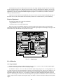
Factory-Configured Switch and Jumper Settings
Table 1-1 lists the factory settings of the user-configurable jumper and switches on the DA800 board. Figure 1-1 shows the board layout and the locations of the factory-set jumpers. The following paragraphs explain how
to change the factory settings. Pay special attention to the setting of S1, the base address switch, to avoid address
contention when you first use your board in your system.
Table 1-1: Factory Settings
Switch/
Jumper
Factory Settings
(Jumpers Installed)
Function Controlled
P3
Connects the interrupt source selected on P4 to
an interrupt channel, IRQ2-IRQ7; pulls tri-state
buffer to ground for multiple interrupt applications
All channels disabled; G (ground for
buffer) connected
P4
Selects the interrupt source
EXT
P5
Sets the clock sources for the three 8254
timer/counters (TC0-TC2)
CLK0-OSC; CLK1-OT0; CLK2-OT1
(all 3 timer/counters cascaded)
P7
Configures the output voltage range or current
loop settings for DAC1
Jumpers installed on ±5, X1, VEN,
VOUT to set output at -5 to +5 volts
P8
Configures the output voltage range or current
loop settings for DAC2
Jumpers installed on ±5, X1, VEN,
VOUT to set output at -5 to +5 volts
P9
Configures the output voltage range or current
loop settings for DAC3
Jumpers installed on ±5, X1, VEN,
VOUT to set output at -5 to +5 volts
P10
Configures the output voltage range or current
loop settings for DAC4
Jumpers installed on ±5, X1, VEN,
VOUT to set output at -5 to +5 volts
S1
Sets the base address
300 hex (768 decimal)
S2
Bypasses 8255 Port A buffers for Mode 2
operation
Open (buffers not bypassed)
S3
Bypasses 8255 Port C buffers for Mode 1 or Mode
2 operation
Open (buffers not bypassed)
1-3
AOUT1
P10
AOUT4
SWITCH
RN10
XTAL
P7
AOUT2
IEN
IOUT
VEN
VOUT
TR4
X2
TR3
TR2
X1
TR1
5V
+
- 5V
IEN
VOUT
IOUT
VEN
TR8
X2
TR7
X1
TR6
5V
+
- 5V
TR5
BASE ADDRESS
P9
AOUT3
S1
P8
Y1
RN9
C7
U19
C29
C30
RN1
C24
RN8
C18
RN7
U20
U21
C40
AD712
C32
C34
C41
C36
C39
AD694
AD694
P2
AD7237
82C54
U17
U19
C23
C15
C26
C16
AD712
C38
AD694
C17
C28
C27
C33
C31
C42
C35
AD7237
C37
C19
U16
U23
C25
AD694
C5
U5
PB
OT0
CLK1
OSC
EC1
U6
PB
RN2
U18
G
V
PA
U22
RN3
G
V
74HCT245
82C55
U10
PAL
C10
74HCT08
EC0
74LS244
U15
CLK0
OSC
C11
74HCT245
C6
P5
U11
P6
74LS125
PA
SWITCH
OT1
CLK2
V
RN15
U13
P4
C13
PC0
PC3
EXT
OT2
OT0
PCL
PCH
SWITCH
G
C14
RN5
74HCT138
U8
S3
+
C43
+
+
C22
74HCT245
C1
74HCT367
C4
C2
Made in USA
U3
74HCT688
C8
C20
U9
U14
74HCT243
74HCT243
C9
PAL
C21
G
RN4
V
PCL
C3
P3
IRQ
2
U2
+
S2
PCH
R1
EC2
OT1
OSC
U12
R
3
4
5
6
7
G
U1
U4
Real Time Devices, Inc. State College, PA 16804
DA800
,,
Accessing the Analog World
,,
Fig. 1-1 — Board Layout Showing Factory-Configured Settings
P3 — Interrupt Channel Select (Factory Setting: G Connected; Interrupt Channels Disabled)
This header connector, shown in Figure 1-2, lets you connect an interrupt source selected on P4 to an interrupt
channel, IRQ2 through IRQ7. To connect the interrupt source to an interrupt channel, you must install a jumper
across the desired IRQ channel.
The rightmost pair of pins on P3, labeled G, are provided so that you can install a jumper which connects a
1 kilohm pull-down resistor to the output of a high-impedance tri-state driver which carries the interrupt request
signal. This pull-down resistor drives the interrupt request line low whenever interrupts are not active. So, whenever
an interrupt request is made, the tri-state buffer is enabled, forcing the output high and causing an interrupt. You can
monitor the interrupt status through bit 0 in the status word (I/O address location BA + 15). After the interrupt has
been serviced, the clear command returns the IRQ line low, disabling the tri-state buffers, and pulling the output low
again. Figure 1-3 shows this circuit. Because the interrupt request line is driven low only by the pull-down resistor,
you can have two or more boards which share the same IRQ channel. You can tell which board issued the interrupt
request by monitoring each board’s IRQ status bit.
NOTE: When you use multiple boards that share the same interrupt, only one board should have the G ground
jumper installed. The rest should be disconnected. Whenever you operate a single board, the G jumper should be
installed.
P3
IRQ
2
3
4
5
6
7
G
Fig. 1-2 — Interrupt Channel Select Jumper, P3
1-4
I NT
SOURCE
I RQ STAT US
CLK
I NTERRUP T
R E GI S TE R
+5 V
I NT ERRUPT
CLR
CLR
P3
G
Fig. 1-3 — Pulling Down the Interrupt Request Line
P4 — Interrupt Source Select (Factory Setting: EXT)
This header connector, shown in Figure 1-4, lets you connect one of six interrupt sources for interrupt generation. These sources are: OT0, OT1, and OT2, which are the three 8254 timer/counter outputs; PC3, which is the
INTRA signal from the 8255 PPI; PC0, which is the INTRB signal from the 8255 PPI; and EXT, an external
interrupt you can route onto the board through the P2 I/O connector. To connect an interrupt source, place the
jumper across the desired set of pins. Note that only ONE interrupt source can be activated at a time.
PC0
PC3
EXT
OT2
OT1
OT0
P4
Fig. 1-4 — Interrupt Source Select Jumper, P4
P5 — 8254 Timer/Counter Clock Sources (Factory Settings: CLK0-XTAL, CLK1-OUT0, CLK2-OUT1)
This header connector, shown in Figure 1-5, lets you select the clock sources for the 8254 timer/counters, TC0,
TC1, and TC2. The factory setting cascades all three timer/counters, with the clock source for TC0 being the onboard 8 MHz oscillator, the output of TC0 providing the clock for TC1, and the output of TC1 providing the clock
for TC2. You can connect any or all of the sources to an external clock input through the P2 I/O connector, or you
can set TC1 and TC2 to be clocked by the 8 MHz oscillator. Figure 1-6 shows a block diagram of the timer/counter
circuitry to help you with these connections.
NOTE: When installing jumpers on this header, make sure that only one jumper is installed in each group of
two or three CLK pins.
CLK0
OSC
EC0
CLK1
OT0
P5
OSC
EC1
CLK2
OT1
OSC
EC2
Fig. 1-5 — 8254 Timer/Counter Clock Source Jumpers, P5
1-5
8 00
I/O CONNECTOR
P2
8254
P5
CLK0
TIMER/
COUNTER
0
OSC (8 MHz)
PIN 39
CLK
+5 V
GATE
OUT
OUT0
TIMER/
COUNTER
1
EXT CLK 0
PIN 19
EXT GATE 0
PIN 40
T/C OUT 0
PIN 43
EXT CLK 1
PIN 41
EXT GATE 1
PIN 42
T/C OUT 1
PIN 45
EXT CLK 2
PIN 46
EXT GATE 2
PIN 44
T/C OUT 2
CLK1
CLK
+5 V
GATE
OUT
CLK2
OUT1
TIMER/
COUNTER
2
CLK
+5 V
GATE
OUT
Fig. 1-6 — 8254 Timer/Counter Circuit Block Diagram
P7 Through P10 — DAC1 Through DAC4 Output Range Select (Factory Setting: -5 to +5 Volts)
These identical header connectors, shown in Figure 1-7, let you independently set the output of each D/A
converter to one of four voltage ranges or as a 4-20 mA current loop source. Figure 1-7 shows all five possible
configurations for these headers, and the table below summarizes these settings. The topmost pair of pins, 5V, is
jumpered when operating in a unipolar voltage range or as a current loop. The next pair of pins, ±5V, is jumpered
when operating in a bipolar voltage range (±5 or ±10 volts). The X1 and X2 pins set the range multiplier. When a
jumper is installed across X1, the multiplier is set at times 1 for 0 to +5 and ±5 volt ranges. When the jumper is
installed across X2, the multiplier is times 2 for 0 to +10 and ±10 volt ranges. The VEN pins enable voltage outputs
when a jumper is installed, or the IEN pins enable 4-20 mA current loop operation when a jumper is installed.
Finally, a jumper must be placed across the VO pins for output voltages or across the IO pins for 4-20 mA current
loop operation. To configure each header for your application, install the jumpers as shown in the diagrams on the
next page for the desired output range. The factory setting of each DAC is shown in Figure 1-7a, ±5 volts.
Output Range
Jumpers
(left to right)
±5V
0 to +5V
±10V
0 to +10V
4-20 mA
5V
OFF
ON
OFF
ON
OFF
±5V
ON
OFF
ON
OFF
ON
X1
ON
ON
OFF
OFF
ON
X2
OFF
OFF
ON
ON
OFF
VEN
ON
ON
ON
ON
OFF
IEN
OFF
OFF
OFF
OFF
ON
VOUT
ON
ON
ON
ON
OFF
IOUT
OFF
OFF
OFF
OFF
ON
1-6
IOUT
VOUT
IEN
VEN
X1
X2
IOUT
VOUT
IEN
VEN
X2
Fig. 1-7c — ±10V Output
X1
±5V
5V
Fig. 1-7d — 0 to +10V Output
±5V
5V
IOUT
VOUT
IEN
VEN
X2
X1
IOUT
VOUT
IEN
VEN
Fig. 1-7b — 0 to +5V Output
X2
X1
±5V
5V
±5V
5V
IOUT
VOUT
IEN
VEN
X2
X1
±5V
5V
Fig. 1-7a — ±5V Output
Fig. 1-7e — 4-20 mA Output
Fig. 1-7 — DAC1 Through DAC4 Output Range Select, P7 Through P10
S1 — Base Address (Factory Setting: 300 hex (768 decimal))
One of the most common causes of failure when you are first trying your board is address contention. Some of
your computer’s I/O space is already occupied by internal I/O and other peripherals. When the DA800 board
attempts to use I/O address locations already used by another device, contention results and the board does not work.
To avoid this problem, the DA800 has an easily accessible DIP switch, S1, which lets you select any one of 16
starting addresses in the computer’s I/O. Should the factory setting of 300 hex (768 decimal) be unsuitable for your
system, you can select a different base address simply by setting the switches to any value shown in Table 1-2. The
table shows the switch settings and their corresponding decimal and hexadecimal (in parentheses) values. Make sure
that you verify the order of the switch numbers on the switch (1 through 4) before setting them. When the switches
are pulled forward, they are OPEN, or set to logic 1, as labeled on the DIP switch package. When you set the base
address for your board, record the value in the table inside the back cover. Figure 1-8 shows the DIP switch set for a
base address of 300 hex (768 decimal).
Table 1-2: Base Address Switch Settings, S1
Base Address
Decimal / (Hex)
Switch Setting
4 3 2 1
Base Address
Decimal / (Hex)
Switch Setting
4 3 2 1
512 / (200)
0 0 0 0
768 / (300)
10 0 0
544 / (220)
0 0 0 1
800 / (320)
1 0 0 1
576 / (240)
0 0 1 0
832 / (340)
1 0 1 0
608 / (260)
0 0 1 1
864 / (360)
1 0 1 1
640 / (280)
0 1 0 0
896 / (380)
1 1 0 0
672 / (2A0)
0 1 0 1
928 / (3A0)
11 0 1
704 / (2C0)
0 1 1 0
960 / (3C0)
1 1 1 0
736 / (2E0)
0 1 1 1
992 / (3E0)
1 1 1 1
0 = closed, 1 = open
1-7
Fig. 1-8 — Base Address Switch, S1
S2 and S3 — Buffer Bypass Switches (Factory Setting: OPEN (Not Bypassed))
Mode 1 Operation (S3) — When operating the 8255 in Mode 1, the lines of Port C function as control lines,
some as outputs and some as inputs. When using Mode 1, the Port C buffers must be removed and bypassed to allow
the Port C lines to be individually set as inputs or outputs. Figure 1-9 shows the Port C buffers, and the following
steps tell you how to configure the board for Mode 1 operation.
To remove buffering from Port C:
1. Close DIP switches 1 through 8 on S3.
2. Remove U8 from the board.
3. Remove U9 from the board.
CAUTION: Remember, whenever you close the switches on S3, be sure to remove the buffers, U8 and U9,
from the board. Failure to do so may damage the board.
Mode 2 Operation (S2, S3) — When operating the 8255 in Mode 2, the lines of Port A must be bidirectional
and the lines of Port C function as control lines, some as outputs and some as inputs. When using Mode 2, both the
Port A and Port C buffers must be removed and bypassed. Figure 1-10 shows the Port A buffers, Figure 1-9 shows
the Port C buffers, and the following steps tell you how to configure the board for Mode 2 operation.
To remove buffering from Ports A and C:
1.
2.
3.
4.
5.
Close DIP switches 1 through 8 on S2 (Port A).
Remove U10 from the board.
Close DIP switches 1 through 8 on S3 (Port C).
Remove U8 from the board.
Remove U9 from the board.
CAUTION: Remember, whenever you close the switches on S2 and S3, be sure to remove the buffers, U8,
U9, and U10, from the board. Failure to do so may damage the board.
1-8
800
I/O CONNECTOR
P2 / P6
82C55
PC7
PC6
PC5
BUFFER
U8
PC4
PIN 24
PIN 16
PIN 26
PIN 14
PIN 28
PIN 12
PIN 30
PIN 10
PIN 32
PIN 8
PIN 34
PIN 6
PIN 36
PIN 4
PIN 38
PIN 2
PORT
C
PC3
PC2
PC1
PC0
BUFFER
U9
S3
1
2
3
4
5
6
7
8
Fig. 1-9 — Port C Buffer Circuitry
800
I/O CONNECTOR
P2
82C55
PA7
PIN 23
PA6
PIN 25
PA5
PIN 27
PA4
PIN 29
BUFFER
PORT
A
PA3
U10
PIN 31
PA2
PIN 33
PA1
PIN 35
PA0
PIN 37
S2
1
2
3
4
5
6
7
8
Fig. 1-10 — Port A Buffer Circuitry
1-9
Pull-up/Pull-down Resistors on Digital I/O Lines
The 8255 programmable peripheral interface provides 24 parallel TTL/CMOS compatible digital I/O lines
which can be interfaced with external devices. The lines are divided into four groups: eight Port A lines, eight Port
B lines, four Port C Lower lines, and four Port C Upper lines. You can install and connect pull-up or pull-down
resistors for any or all of these four groups of lines. You may want to pull lines up for connection to switches. This
will pull the line high when the switch is disconnected. Or, you may want to pull down lines connected to relays
which control turning motors on and off. These motors turn on when the digital lines controlling them are high.
Pulling these lines down keeps them from floating high during the brief period between power-up and initialization.
To use the pull-up/pull-down feature, you must first install 10 kilohm resistor packs in any or all of the four
locations around the 8255, labeled PA, PB, PCL, and PCH. PA (RN3) and PB (RN6) take a 10-pin pack, and PCL
(RN4) and PCH (RN5) take 6-pin packs. Figure 1-11 shows these locations.
After the resistor packs are installed, you must connect them into the circuit as pull-ups or pull-downs. Locate
the three-hole pads on the board near the resistor packs. They are labeled G (for ground) on one end and V (for Vcc)
on the other end. The middle hole is common. PA is for Port A, PB for Port B, PCL is for Port C Lower, and PCH is
for Port C Upper. Figure 1-11 shows a blowup of the pull-up/pull-down pads. To operate as pull-ups, solder a
jumper wire between the common pin (middle pin of the three) and the V pin. For pull-downs, solder a jumper wire
between the common pin (middle pin) and the G pin. For example, Figure 1-12 shows Port A lines with pull-ups,
Port C Lower with pull-downs, and Port C Upper with no resistors.
U11
P6
PA
PB
RN6
PB G
C11
V
V
PA
RN3
G
74LS245
74LS245
82C55
U10
C10
V
C13
PCL
RN4
V
AOUT1
P7
AOUT2
IEN
VEN
VOUT
RN10
P10
AOUT4
SWITCH
XTAL
IOUT
TR4
X2
TR3
TR2
X1
TR1
5V
+
- 5V
IEN
IOUT
VEN
VOUT
TR8
X2
TR7
P9
AOUT3
TR6
X1
TR5
BASE ADDRESS
5V
+
- 5V
PCL
S1
G
P8
Y1
RN9
C7
U19
C29
C30
RN1
C24
RN8
C18
RN7
U20
U21
C40
AD712
C32
C34
C41
C36
C39
AD694
AD694
P2
AD7237
82C54
U17
U19
C23
C15
C26
C16
AD712
C28
C27
C33
AD694
C17
C38
C31
C42
C35
AD7237
C37
C19
U16
U23
C25
AD694
C5
U5
PB
P6
U11
P5
U15
EC0
OT0
CLK1
OSC
EC1
U6
RN2
PA
U18
G
V
PA
U22
RN3
G
V
74HCT245
82C55
U10
PAL
C10
74HCT08
CLK0
OSC
74LS244
PB
74HCT245
C6
74LS125
C11
SWITCH
OT1
CLK2
U12
V
RN15
U13
P4
PC0
PC3
OT0
EXT
PCL
C3
RN5
PCH
SWITCH
G
C14
C9
U8
S3
C8
+
+
+
C43
C22
C4
74HCT367
74HCT245
C1
U3
C2
Made in USA
C20
U9
74HCT688
74HCT243
74HCT243
74HCT138
U14
C21
G
RN4
V
PAL
P3
IRQ
2
U2
+
C13
PCL
OT2
EC2
S2
PCH
R1
OT1
OSC
R
3
4
5
6
7
G
U4
Real Time Devices, Inc. State College, PA 16804
U1
DA800
,,
Accessing the Analog World
,,
Fig. 1-11 — Pull-up/Pull-down Resistor Circuitry
1-10
S2
G
PCH
PCH
U13
SWITCH
RN5
+5 V
PA
8255
V
PULL- UP
G
10K
PORT A
(PA0-7)
+5 V
CL
PULL- DOWN
V
G
10K
PORT C
LOWER
( PC0- 3)
+5 V
CH
V
G
PORT C
UPPER
( PC4- 7)
Fig. 1-12 — Adding Pull-ups and Pull-downs to Some Digital I/O Lines
1-11
1-12
CHAPTER 2
BOARD INSTALLATION
The DA800 board is easy to install in your IBM PC/XT/AT or
compatible computer. This chapter tells you step-by-step how to
install and connect the board for voltage outputs and 4-20 mA
current loop outputs.
After you have installed the board and made all of your connections, you can turn your system on and run the 800DIAG board
diagnostics program included on your example software disk to
verify that your board is working.
2-1
2-2
Board Installation
Keep the board in its antistatic bag until you are ready to install it in your computer. When removing it from the
bag, hold the board at the edges and do not touch the components or connectors.
Before installing the board in your computer, check the jumper settings. Chapter 1 reviews the factory settings
and how to change them. If you need to change any settings, refer to the appropriate instructions in Chapter 1. Note
that incompatible jumper settings can result in unpredictable board operation and erratic response.
Also note that the P2 I/O connector mounting bracket has an oversized cutout to allow space for running the
cable to 20-pin on-board connector P6 through the same I/O slot. If you want to run both cables through the same
slot, you must make these connections before installing the board.
To install the board:
1. Turn OFF the power to your computer.
2. Remove the top cover of the computer housing (refer to your owner’s manual if you do not already know
how to do this).
3. Select any unused short or full-size expansion slot and remove the slot bracket.
4. Touch the metal housing of the computer to discharge any static buildup and then remove the board from its
antistatic bag.
5. Holding the board by its edges, orient it so that its card edge (bus) connector lines up with the expansion slot
connector in the bottom of the selected expansion slot.
6. After carefully positioning the board in the expansion slot so that the card edge connector is resting on the
computer’s bus connector, gently and evenly press down on the board until it is secured in the slot.
NOTE: Do not force the board into the slot. If the board does not slide into place, remove it and try again.
Wiggling the board or exerting too much pressure can result in damage to the board or to the computer.
7. After the board is installed, secure the slot bracket back into place and put the cover back on your computer.
The board is now ready to be connected via the external I/O connector at the rear panel of your computer.
2-3
External I/O Connections
Figure 2-1 shows the DA800’s P2 I/O connector pinout and P6 on-board I/O connector pinout. Refer to these
diagrams as you make your I/O connections.
AOUT1
1
2
ANALOG GND
PB0
1
2
PC0
AOUT2
3
4
ANALOG GND
PB1
3
4
PC1
AOUT3
5
6
ANALOG GND
PB2
5
6
PC2
AOUT4
7
8
ANALOG GND
PB3
7
8
PC3
ANALOG GND
9
10
ANALOG GND
PB4
9
10
PC4
ANALOG GND
11 12
ANALOG GND
PB5
11 12
PC5
ANALOG GND
13 14
ANALOG GND
PB6
13 14
PC6
ANALOG GND
15 16
ANALOG GND
PB7
15 16
PC7
+12 VOLTS
17 18
+5 VOLTS
-12 VOLTS
19 20
DIGITAL GND
EXT INT
17 18
DIGITAL GND
EXT GATE 0
19 20
DIGITAL GND
DIGITAL GND
21 22
DIGITAL GND
PA7
23 24
PC7
PA6
25 26
PC6
PA5
27 28
PC5
PA4
29 30
PC4
PA3
31 32
PC3
PA2
33 34
PC2
PA1
35 36
PC1
PA0
37 38
PC0
EXT CLK 0
39 40
T/C OUT 0
EXT GATE 1
41 42
T/C OUT 1
EXT CLK 1
43 44
T/C OUT 2
EXT CLK 2
45 46
EXT GATE 2
+12 VOLTS
47 48
+5 VOLTS
-12 VOLTS
49 50
DIGITAL GND
P6
20-pin on-board I/O connector
P2
50-pin I/O connector
Fig. 2-1 — P2 and P6 I/O Connector Pin Assignments
Connecting the Analog Outputs — Voltage Outputs
When the analog output is configured as a voltage output, the high side of the device receiving the output is
connected to an AOUT line and the low side is connected to the corresponding ANALOG GND. Figure 2-2 shows
how to connect the DA800 voltage outputs to a load.
Connecting the Analog Outputs — 4-20 mA Current Loop Outputs
When the analog output is configured as a 4-20 mA current loop source, you can operate the loop using only the
+12 volts supplied to the DA800 to power the current loop transmitters, or you can use external power supplies for
dual power supply operation.
Current Loop Operation, No Loop Power Supply: Figure 2-3 shows how to connect the current loop
transmitter outputs to a resistive load with no external loop supply. The AD694 current loop transmitters used on the
DA800 are designed to be stable when driving resistive loads. For inductive or poorly defined loads, it is recommended that you add a 0.01 µF capacitor in the location provided on the board for each analog output channel. The
table included in Figure 2-3 lists each channel and its corresponding capacitor number on the board. These capacitors are located with the analog output circuitry on the top half of the board. The capacitor is placed between the
output of the AD694 and analog ground, as shown in the circled area of Figure 2-3.
2-4
800
I/ O CONNECTOR
P2
OP- AMP
BUFFERS
PIN 1
AD7 1 2
AOUT 1
LOAD
AD7 1 2
PIN 2
ANALOG GND
PIN 7
AOUT 4
LOAD
PIN 8
ANALOG GND
Fig. 2-2 — Voltage Output Connections
CURRENT LOOP
TRANSMITTERS
800
I/ O CONNECTOR
P2
AD694
PIN 1
AOUT1
AD6 9 4
PIN 1
C24
.01 µF
AOUT 1
LOAD
PIN 2
AD6 9 4
PIN 7
ANALOG GND
AOUT 4
Channel
Capacitor
AOUT1
C24
AOUT2
C26
AOUT3
C28
AOUT4
C30
LOAD
PIN 8
ANALOG GND
Fig. 2-3 — Current Output Connections, No Loop Supply
2-5
Current Loop Operation, Single Loop Power Supply: Figure 2-4 shows how to connect the current loop
transmitter outputs to corresponding loads with a single external loop supply not exceeding 24 volts. The AD694
current loop transmitters used on the DA800 are powered through the board by +12 volts. When operated with a
+12 volt supply, the AD694 can source a current to a point as low as 24 volts below common.
WARNING!! Be sure to observe the correct polarity when connecting the external
loop supply. The positive terminal is connected to ANALOG GND, and the negative
terminal is connected to the load side, as shown in the diagram! Failure to properly
connect the supply can damage the board.
Current Loop Operation, Multiple Loop Power Supplies: Figure 2-5 shows how to connect the current loop
transmitter outputs to corresponding loads with an external loop supply not exceeding 24 volts in each loop.
WARNING!! Be sure to observe the correct polarity when connecting the external
loop supplies. The positive terminal is connected to ANALOG GND, and the negative
terminal is connected to the load side, as shown in the diagram! Failure to properly
connect the supply can damage the board.
Connecting the Timer/Counters and Digital I/O
For all of the digital connections, the high side of an external signal source or destination device is connected to
the appropriate signal pin on the P2 or P6 I/O connector, and the low side is connected to any DIGITAL GND.
Running the 800DIAG Diagnostics Program
Now that your board is ready to use, you will want to try it out. An easy-to-use, menu-driven diagnostics
program, 800DIAG, is included with your example software to help you verify your board’s operation. You can also
use this program to make sure that your current base address setting does not contend with another device.
2-6
CURRENT LOOP
TRANSMITTERS
AD6 9 4
800
I/ O CONNECTOR
P2
PIN 1
AOUT 1
LOAD
PIN 2
AD6 9 4
PIN 7
AOUT 4
LOAD
PIN 8
+
ANALOG GND
LOOP
SUPPLY
2 4 V MAX
-
Fig. 2-4 — Current Output Connections, Single Loop Supply
CURRENT LOOP
TRANSMITTERS
AD6 9 4
800
I/ O CONNECTOR
P2
PIN 1
AOUT 1
LOAD
AD6 9 4
PIN 2
ANALOG GND
PIN 7
AOUT 4
+
LOOP
SUPPLY
2 4 V MAX
-
LOAD
PIN 8
ANALOG GND
+
LOOP
SUPPLY
2 4 V MAX
-
Fig. 2-5 — Current Output Connections, Multiple Loop Supplies
2-7
2-8
CHAPTER 3
HARDWARE DESCRIPTION
This chapter describes the features of the DA800 . The three
major circuits are the D/A, the timer/counters, and the digital I/O.
This chapter also describes the hardware-selectable interrupts.
3-1
3-2
The DA800 provides four analog output channels with voltage or 4-20 mA current loop outputs, three 16-bit
timer/counters, and 24 TTL/CMOS digital I/O lines, as shown Figure 3-1. This chapter describes the hardware
which makes up the major circuits and hardware-selectable interrupts.
ADDRESS
ADDRESS
DECODE
AOUT1
V/I SELECT
12-BIT
D/A
CONVERTER
AOUT2
V/I SELECT
AOUT3
V/I SELECT
12-BIT
D/A
CONVERTER
AOUT4
V/I SELECT
8255
PPI
24
BUFFERS
AND
PULL-UP/DOWN
RESISTORS
8
ON BOARD CONNECTOR
8
16
2
3
8254
PIT
DATA
8 MHz
OSC
TIMER/
COUNTER
I/O
SELECT
I/O CONNECTOR
PC BUS
INTERRUPT
SELECT
9
EXTINT
±12 VOLTS
CONTROL
+5 VOLTS
Fig. 3-1 — DA800 Block Diagram
D/A Conversion
The DA800 board performs digital-to-analog conversions on four independent analog output channels. The
output of each conversion channel is jumper-selectable for ±5, ±10, 0 to +5, or 0 to +10 volts, or as a 4-20 mA
current loop source.
The AD7237 12-bit D/A converter contains two independent D/A converter channels in a single CMOS
package. The data to be converted is double buffered at the D/A input, which allows simultaneous updating of all
eight D/A output channels.
For voltage outputs, the AD712 precision operational amplifier provides complete coverage of the output
voltage ranges. The exceptionally low offset voltage and drift ensure an accurate analog output on each channel.
For current loop outputs, the AD694 current loop transmitter converts the voltage output of the D/A converter to
a corresponding current between 4 and 20 mA.
Digital I/O, 8255 Programmable Peripheral Interface
The 8255 programmable peripheral interface (PPI) can be easily configured to solve a wide range of digital
real-world problems. This high-performance TTL/CMOS compatible chip has 24 parallel programmable digital I/O
lines divided into two groups of 12 lines each:
Group A — Port A (8 lines) and Port C Upper (4 lines);
Group B — Port B (8 lines) and Port C Lower (4 lines).
3-3
Each group can be programmed for one of three modes of operation. When operating in Mode 1, the on-board
buffers must be removed from the Port C lines. When operating in Mode 2, both Port A and Port C buffering must
be removed. This procedure is described in Chapter 1 in the S2 and S3 DIP switch discussion. The three operating
modes are:
Mode 0 — Basic input/output. Lets you use simple input and output operation for a port. Data is written to or
read from the specified port.
Mode 1 — Strobed input/output. Lets you transfer I/O data from Port A in conjunction with strobes or handshaking signals.
Mode 2 — Strobed bidirectional input/output. Lets you communicate bidirectionally with an external device
through Port A. Handshaking is similar to Mode 1.
These modes are detailed in the 8255 Data Sheet, reprinted from Intel in Appendix C.
The bidirectional buffers on the 8255’s I/O lines monitor the 8255 control word to automatically set their
direction. Hardware changes to the buffer circuitry are required only when using Mode 1 or Mode 2, where the Port
A and/or Port C buffers must be removed as described in Chapter 1.
Timer/Counters
An 8254 programmable interval timer provides three 16-bit, 8 MHz timer/counters to support a wide range of
timing and counting functions. These timer/counters can be cascaded or used individually for many applications.
Each timer/counter has two inputs, CLK in and GATE in, and one output, timer/counter OUT. The clock
sources for the timer/counters can be selected using jumpers on header connector P5 (see Chapter 1). The timer/
counters can be programmed as binary or BCD down counters by writing the appropriate data to the command word,
as described in Chapter 4. The command word also lets you set up the mode of operation. The six programmable
modes are:
Mode 0
Mode 1
Mode 2
Mode 3
Mode 4
Mode 5
Event Counter (Interrupt on Terminal Count)
Hardware-Retriggerable One-Shot
Rate Generator
Square Wave Mode
Software-Triggered Strobe
Hardware Triggered Strobe (Retriggerable)
These modes are detailed in the 8254 Data Sheet, reprinted from Intel in Appendix C.
Interrupts
The DA800 can use any one of six signal sources to generate interrupts. These sources are: OT0, OT1, and
OT2, which are the three 8254 timer/counter outputs; PC3, which is the INTRA signal from the 8255 PPI; PC0,
which is the INTRB signal from the 8255 PPI; and EXT, an external interrupt you can route onto the board through
the P2 I/O connector. Chapter 1 tells you how to set the jumpers on interrupt header connectors P3 and P4, and
Chapter 4 provides some programming information.
3-4
CHAPTER 4
BOARD OPERATION AND PROGRAMMING
This chapter shows you how to program and use your DA800
board. It provides a complete description of the I/O map and
programming operations to aid you in programming. The example
programs included on the disk in your board package are listed at
the end of this chapter. These programs, written in Turbo C, Turbo
Pascal, and BASIC, include source code to simplify your
applications programming.
4-1
4-2
Defining the I/O Map
The I/O map for the DA800 is shown in Table 4-1 below. As shown, the board occupies 20 consecutive I/O port
locations. The base address (designated as BA) can be selected using DIP switch S1 as described in Chapter 1,
Board Settings. This switch can be accessed without removing the board from the connector. The following sections
describe the register contents of each address used in the I/O map.
Table 4-1: DA800 I/O Map
Register Description
Address *
(Decimal)
8255 PPI Port C
Write Function
Program Port A digital output
Read Port A digital input lines lines
Program Port B digital output
Read Port B digital input lines lines
Program Port C digital output
Read Port C digital input lines lines
8255 PPI Control Word
Reserved
Program PPI configuration
BA + 3
D/A Converter 1 LSB
Reserved
Program DAC1 LSB
BA + 4
D/A Converter 1 MSB
Reserved
Program DAC1 MSB
BA + 5
D/A Converter 2 LSB
Reserved
Program DAC2 LSB
BA + 6
D/A Converter 2 MSB
Reserved
Program DAC2 MSB
BA + 7
D/A Converter 3 LSB
Reserved
Program DAC3 LSB
BA + 8
D/A Converter 3 MSB
Reserved
Program DAC3 MSB
BA + 9
D/A Converter 4 LSB
Reserved
Program DAC4 LSB
BA + 10
D/A Converter 4 MSB
Reserved
BA + 11
Update All DACs
Reserved
Program DAC4 MSB
Updates the outputs of all
DACs
Reserved
Reserved
BA + 13
IRQ Enable
Reserved
Reserved
Enable and disable interrupt
generation
Interrupt Status/Clear
Read status of interrupt
Clear interrupt
BA + 15
8254 Timer/Counter 0
Read TC0 count value
Load TC0 count register
BA + 16
8254 Timer/Counter 1
Read TC1 count value
Load TC1 count register
BA + 17
8254 Timer/Counter 2
Read TC2 count value
Load TC2 count register
BA + 18
8254 Control Word
Reserved
Program control register
BA + 19
8255 PPI Port A
8255 PPI Port B
Read Function
* BA = Base Address
4-3
BA + 0
BA + 1
BA + 2
BA + 12
BA + 14
BA + 0: PPI Port A — Digital I/O (Read/Write)
Transfers the 8-bit Port A digital input and digital output data between the board and an external device. A read
transfers data from the external device, through P2, and into PPI Port A; a write transfers the written data from
Port A through P2 to an external device.
BA + 1: PPI Port B — Digital I/O (Read/Write)
Transfers the 8-bit Port B digital input and digital output data between the board and an external device. A read
transfers data from the external device, through on-board I/O connector P6, and into PPI Port B; a write transfers the
written data from Port B through P6 to an external device.
BA + 2: PPI Port C — Digital I/O (Read/Write)
Transfers the two 4-bit Port C digital input and digital output data groups (Port C Upper and Port C Lower)
between the board and an external device. A read transfers data from the external device, through P2 and on-board
I/O connector P6, and into PPI Port C; a write transfers the written data from Port C through P2 and P6 to an
external device.
BA + 3: 8255 PPI Control Word (Write Only)
When bit 7 of this word is set to 1, a write programs the PPI configuration. The table at the top of the next page
shows the control words for the 16 possible Mode 0 Port I/O combinations.
D7 D6 D5 D4 D3 D2 D1 D0
Mode Set Flag
1 = active
Port C Lower
0 = output
1 = input
Mode Select
00 = mode 0
01 = mode 1
1x = mode 2
Port B
0 = output
1 = input
Port A
0 = output
1 = input
Group A
Port C Upper
0 = output
1 = input
4-4
Mode Select
0 = mode 0
1 = mode 1
Group B
8255 Port I/O Flow Direction and Control Words, Mode 0
Group A
Group B
Control Word
Port A
Port C Upper
Port B
Port C Lower
Binary
Decimal
Hex
Output
Output
Output
Output
10000000
128
80
Output
Output
Output
Input
10000001
129
81
Output
Output
Input
Output
10000010
130
82
Output
Output
Input
Input
10000011
131
83
Output
Input
Output
Output
10001000
136
88
Output
Input
Output
Input
10001001
137
89
Output
Input
Input
Output
10001010
138
8A
Output
Input
Input
Input
10001011
139
8B
Input
Output
Output
Output
10010000
144
90
Input
Output
Output
Input
10010001
145
91
Input
Output
Input
Output
10010010
146
92
Input
Output
Input
Input
10010011
147
93
Input
Input
Output
Output
10011000
152
98
Input
Input
Output
Input
10011001
153
99
Input
Input
Input
Output
10011010
154
9A
Input
Input
Input
Input
10011011
155
9B
When bit 7 of this word is set to 0, a write can be used to individually program the Port C lines.
D7 D6 D5 D4 D3 D2 D1 D0
Set/Reset
Function Bit
0 = active
Bit Select
000 = PC0
001 = PC1
010 = PC2
011 = PC3
100 = PC4
101 = PC5
110 = PC6
111 = PC7
4-5
Bit Set/Reset
0 = set bit to 0
1 = set bit to 1
For example, if you want to set Port C bit 0 to 1, you would set up the control word so that bit 7 is 0; bits 1, 2,
and 3 are 0 (this selects PC0); and bit 0 is 1 (this sets PC0 to 1). The control word is set up like this:
0
Sets PC0 to 1:
(written to BA +3)
X
X
X
0
0
0
1
D7 D6 D5 D4 D3 D2 D1 D0
X = don’t care
Set PC0
Set/Reset
Function Bit
Bit Select
000 = PC0
BA + 4: D/A Converter 1 LSB (Write Only)
Programs the DAC1 LSB (eight bits).
BA + 5: D/A Converter 1 MSB (Write Only)
Programs the DAC1 MSB (four bits) into D0 through D3; D4 through D7 are irrelevant.
BA + 6: D/A Converter 2 LSB (Write Only)
Programs the DAC2 LSB (eight bits).
BA + 7: D/A Converter 2 MSB (Write Only)
Programs the DAC2 MSB (four bits) into D0 through D3; D4 through D7 are irrelevant.
BA + 8: D/A Converter 3 LSB (Write Only)
Programs the DAC3 LSB (eight bits).
BA + 9: D/A Converter 3 MSB (Write Only)
Programs the DAC3 MSB (four bits) into D0 through D3; D4 through D7 are irrelevant.
BA + 10: D/A Converter 4 LSB (Write Only)
Programs the DAC4 LSB (eight bits).
BA + 11: D/A Converter 4 MSB (Write Only)
Programs the DAC4 MSB (four bits) into D0 through D3; D4 through D7 are irrelevant.
DAC LSB
D7 D6 D5 D4 D3 D2 D1 D0
Bit 7
DAC MSB
Bit 6
Bit 5
Bit 4
Bit 3
Bit 2
Bit 1
Bit 0
D7 D6 D5 D4 D3 D2 D1 D0
X
X
X
X
Bit 11
Bit 10
Bit 9
Bit 8
BA + 12: Update DAC Outputs (Write Only)
A write simultaneously starts a D/A conversion in all eight channels (data written is irrelevant). If the data has
not been updated since the last conversion, the output of the DAC will not change.
BA + 13: Reserved
4-6
BA + 14: IRQ Enable (Write Only)
Enables and disables interrupt generation. Writing a “1” enables interrupt generation; writing a “0” disables
interrupt generation.
D7 D6 D5 D4 D3 D2 D1 D0
0
0
0
0
0
0
0
Interrupt Enable/Disable
0 = interrupt disabled
1 = interrupt enabled
BA + 15: Interrupt Status/Clear (Read/Write)
A read shows the status of the interrupt (bit 0 only) as defined below. A write clears the interrupt (data written is
irrelevant). Each time the interrupt status bit goes high, a write should follow to clear the bit.
D7 D6 D5 D4 D3 D2 D1 D0
X
X
X
X
X
X
X
Interrupt Status
0 = no interrupt
1 = interrupt has occurred
BA + 16: 8254 Timer/Counter 0 (Read/Write)
A read shows the count in the counter, and a write loads the counter with a new value. Counting begins as soon
as the count is loaded.
BA + 17: 8254 Timer/Counter 1 (Read/Write)
A read shows the count in the counter, and a write loads the counter with a new value. Counting begins as soon
as the count is loaded.
BA + 18: 8254 Timer/Counter 2 (Read/Write)
A read shows the count in the counter, and a write loads the counter with a new value. Counting begins as soon
as the count is loaded.
BA + 19: 8254 Control Word (Write Only)
Accesses the 8254 control register to directly control the three timer/counters.
D7 D6 D5 D4 D3 D2 D1 D0
BCD/Binary
0 = binary
1 = BCD
Counter Select
00 = Counter 0
01 = Counter 1
10 = Counter 2
11 = read back setting
Read/Load
00 = latching operation
01 = read/load LSB only
10 = read/load MSB only
11 = read/load LSB, then MSB
4-7
Counter Mode Select
000 = Mode 0, event count
001 = Mode 1, programmable 1-shot
010 = Mode 2, rate generator
011 = Mode 3, square wave rate generator
100 = Mode 4, software-triggered strobe
101 = Mode 5, hardware-triggered strobe
Programming the DA800
This section gives you some general information about programming and the DA800 board, and then walks you
through the major DA800 programming functions. These descriptions will help you as you use the example programs included with the board. All of the program descriptions in this section use decimal values unless otherwise
specified.
The DA800 is programmed by writing to and reading from the correct I/O port locations on the board. These
I/O ports were defined in the previous section. Most high-level languages such as BASIC, Pascal, C, and C++, and
of course assembly language, make it very easy to read/write these ports. The table below shows you how to read
from and write to I/O ports using some popular programming languages.
/DQJXDJH
%$6,&
7XUER&
7XUER3DVFDO
$VVHPEO\
5HDG
'DWD ,13$GGUHVV
:ULWH
287$GGUHVV'DWD
'DWD LQSRUWE$GGUHVV RXWSRUWE$GGUHVV'DWD
'DWD 3RUW>$GGUHVV@
3RUW>$GGUHVV@ 'DWD
PRYG[$GGUHVV
LQDOG[
PRYG[$GGUHVV
PRYDO'DWD
RXWG[DO
In addition to being able to read/write the I/O ports on the DA800, you must be able to perform a variety of
operations that you might not normally use in your programming. The table below shows you some of the operators
discussed in this section, with an example of how each is used with Pascal, C, and BASIC. Note that the modulus
operator is used to retrieve the least significant byte (LSB) of a two-byte word, and the integer division operator is
used to retrieve the most significant byte (MSB).
/DQJXDJH
0RGXOXV
,QWHJHU'LYLVLRQ
$1'
25
&
D EF
D EF
D EF
_
D E_F
3DVFDO
02'
D E02'F
',9
D E',9F
$1'
D E$1'F
25
D E25F
%$6,&
02'
D E02'F
?
D E?F
$1'
D E$1'F
25
D E25F
Many compilers have functions that can read/write either 8 or 16 bits from/to an I/O port. For example, Turbo
Pascal uses Port for 8-bit port operations and PortW for 16 bits, Turbo C uses inportb for an 8-bit read of a port
and inport for a 16-bit read. Be sure to use only 8-bit operations with the DA800!
4-8
Clearing and Setting Bits in a Port
When you clear or set one or more bits in a port, you must be careful that you do not change the status of the
other bits. You can preserve the status of all bits you do not wish to change by proper use of the AND and OR
binary operators. Using AND and OR, single or multiple bits can be easily cleared in one operation.
To clear a single bit in a port, AND the current value of the port with the value b, where b = 255 - 2 bit.
Example: Clear bit 5 in a port. Read in the current value of the port, AND it with 223
(223 = 255 - 25), and then write the resulting value to the port. In BASIC, this is programmed as:
V = INP(PortAddress)
V = V AND 223
OUT PortAddress, V
To set a single bit in a port, OR the current value of the port with the value b, where b = 2bit.
Example: Set bit 3 in a port. Read in the current value of the port, OR it with 8 (8 = 23), and then
write the resulting value to the port. In Pascal, this is programmed as:
V := Port[PortAddress];
V := V OR 8;
Port[PortAddress] := V;
Setting or clearing more than one bit at a time is accomplished just as easily. To clear multiple bits in a port,
AND the current value of the port with the value b, where b = 255 - (the sum of the values of the bits to be cleared).
Note that the bits do not have to be consecutive.
Example: Clear bits 2 ,4, and 6 in a port. Read in the current value of the port, AND it with 171
(171 = 255 - 22 - 24 - 26), and then write the resulting value to the port. In C, this is programmed
as:
v = inportb(port_address);
v = v & 171;
outportb(port_address, v);
To set multiple bits in a port, OR the current value of the port with the value b, where b = the sum of the
individual bits to be set. Note that the bits to be set do not have to be consecutive.
Example: Set bits 3, 5, and 7 in a port. Read in the current value of the port, OR it with 168
(168 = 23 + 25 + 27), and then write the resulting value back to the port. In assembly language, this
is programmed as:
mov dx, PortAddress
in al, dx
or al, 168
out dx, al
Often, assigning a range of bits is a mixture of setting and clearing operations. You can set or clear each bit
individually or use a faster method of first clearing all the bits in the range then setting only those bits that must be
set using the method shown above for setting multiple bits in a port. The following example shows how this twostep operation is done.
Example: Assign bits 3, 4, and 5 in a port to 101 (bits 3 and 5 set, bit 4 cleared). First, read in the
port and clear bits 3, 4, and 5 by ANDing them with 199. Then set bits 3 and 5 by ORing them
with 40, and finally write the resulting value back to the port. In C, this is programmed as:
v = inportb(port_address);
v = v & 199;
v = v | 40;
outportb(port_address, v);
4-9
A final note: Don’t be intimidated by the binary operators AND and OR and try to use operators for which you
have a better intuition. For instance, if you are tempted to use addition and subtraction to set and clear bits in place
of the methods shown above, DON’T! Addition and subtraction may seem logical, but they will not work if you try
to clear a bit that is already clear or set a bit that is already set. For example, you might think that to set bit 5 of a
port, you simply need to read in the port, add 32 (25) to that value, and then write the resulting value back to the port.
This works fine if bit 5 is not already set. But, what happens when bit 5 is already set? Bits 0 to 4 will be unaffected
and we can’t say for sure what happens to bits 6 and 7, but we can say for sure that bit 5 ends up cleared instead of
being set. A similar problem happens when you use subtraction to clear a bit in place of the method shown above.
Now that you know how to clear and set bits, we are ready to look at the programming steps for the DA800
board functions.
D/A Conversions
D/A conversions are performed on the four analog output channels, AOUT1 through AOUT4, by writing data to
the D/A converter registers and then issuing an update command (BA + 12) which simultaneously updates the
outputs of all four channels.
The 12-bit digital data for each channel is loaded in a two step process, LSB followed by MSB. After the data
has been loaded for all desired channels, the channels are simultaneously updated by issuing the update command. If
a channel’s data has not been updated since the last conversion, the output of the DAC will not change. The digital
data is converted to a corresponding voltage or 4-20 mA current loop value which is present at the output until new
data is loaded and another update command is issued.
The output voltage ranges or current loop operation are determined by the settings of the AOUT channel
jumpers on P7 through P10. The following tables show key digital inputs and their corresponding outputs for
unipolar and bipolar voltage ranges and for 4-20 mA current loop transmission. The resolution for 0 to +5 volts is
1.22 millivolts; for 0 to +10 and ±5 volts, 2.44 millivolts; for ±10 volts, 4.88 millivolts, and for 4-20 mA current
loop, .0039 mA.
D/A Converter Unipolar Calibration Table
Ideal Output Voltage (in millivolts)
D/A Bit Weight
0 to +5 V
0 to +10 V
4095 (Max. Output)
4998.8
9997.6
2048
2500.0
5000.0
1024
1250.0
2500.0
512
625.00
256
312.50
625.00
128
156.250
312.50
64
78.125
156.250
32
39.063
78.125
16
19.5313
39.063
8
9.7656
19.5313
4
4.8828
9.7656
2
2.4414
4.8828
1
1.2207
2.4414
0
0.0000
0.0000
4-10
1250.0
D/A Converter Bipolar Calibration Table
Ideal Output Voltage (in millivolts)
D/A Bit Weight
±5 V
±10 V
4095 (Max. Output)
+4997.6
+9995.1
2048
0.0
0.0
1024
-2500.0
-5000.0
512
-3750.0
-7500.0
256
-4375.0
-8750.0
128
-4687.5
-9375.0
64
-4843.8
-9687.5
32
-4921.9
-9843.8
16
-4960.9
-9921.9
8
-4980.5
-9960.9
4
-4990.2
-9980.5
2
-4995.1
-9990.2
1
-4997.6
-9995.1
0
-5000.0
-10000.0
D/A Converter 4-20 mA Current Loop Calibration
Table
D/A Bit Weight
Ideal Output Current
(in millamperes)
4095 (Max. Output)
19.9961
2048
12.0000
1024
8.0000
512
6.0000
256
5.0000
128
4.5000
64
4.2500
32
4.1250
16
4.0625
8
4.0313
4
4.0156
2
4.0078
1
4.0039
0
4.0000
4-11
Initializing the 8255 PPI
Before you can use the 24 8255 based digital I/O lines on your DA800, the 8255 must be initialized. This step
must be executed every time you start up, reset, or reboot your computer.
The 8255 is initialized by writing the appropriate control word to I/O port BA + 3. The contents of your control
word will vary, depending on how you want to configure your I/O lines. Use the control word description in the
previous I/O map section to help you program the right value. In the example below, a decimal value of 128 sets up
the 8255 so that all I/O lines are Mode 0 outputs.
1
0
0
0
0
0
0
0
D7 D6 D5 D4 D3 D2 D1 D0
Digital I/O Operations
Once the 8255 is initialized, you can use the digital I/O lines to control or monitor external devices.
Timer/Counters
An 8254 programmable interval timer provides three 16-bit, 8-MHz timer/counters for timing and counting
functions such as frequency measurement, event counting, and interrupts. All three timer/counters are cascaded at
the factory. Figure 4-1 shows the timer/counter circuitry.
Each timer/counter has two inputs, CLK in and GATE in, and one output, timer/counter OUT. They can be
programmed as binary or BCD down counters by writing the appropriate data to the command word, as described in
the I/O map section at the beginning of this chapter.
One of two clock sources, the on-board 8-MHz crystal or an external clock routed through I/O connector P2 can
be selected as the clock input to each timer/counter. In addition, the timer/counters can be cascaded by connecting
TC0’s output to TC1’s clock input and TC1’s output to TC2’s clock input. The diagram shows how these clock
sources are connected to the timer/counters.
8 00
I/O CONNECTOR
P2
8254
P5
CLK0
TIMER/
COUNTER
0
OSC (8 MHz)
CLK
+5 V
GATE
OUT
OUT0
TIMER/
COUNTER
1
PIN 39
EXT CLK 0
PIN 19
EXT GATE 0
PIN 40
T/C OUT 0
PIN 43
EXT CLK 1
PIN 41
EXT GATE 1
PIN 42
T/C OUT 1
PIN 45
EXT CLK 2
PIN 46
EXT GATE 2
PIN 44
T/C OUT 2
CLK1
CLK
+5 V
GATE
OUT
CLK2
OUT1
TIMER/
COUNTER
2
CLK
+5 V
GATE
OUT
Fig. 4-1 — 8254 Timer/Counter Circuit Block Diagram
4-12
An external gate source can be connected to each timer/counter through P2. When a gate is disconnected, an onboard pull-up resistor automatically pulls the gate high, enabling the timer/counter.
The output from each timer/counter is available at P2, where it can be used for interrupt generation or for
counting functions.
The timer/counters can be programmed to operate in one of six modes, depending on your application. The
following paragraphs briefly describe each mode. The 8254 data sheet included in Appendix C provides more
detailed information.
Mode 0, Event Counter (Interrupt on Terminal Count). This mode is typically used for event counting.
While the timer/counter counts down, the output is low, and when the count is complete, it goes high. The output
stays high until a new Mode 0 control word is written to the timer/counter.
Mode 1, Hardware-Retriggerable One-Shot. The output is initially high and goes low on the clock pulse
following a trigger to begin the one-shot pulse. The output remains low until the count reaches 0, and then goes high
and remains high until the clock pulse after the next trigger.
Mode 2, Rate Generator. This mode functions like a divide-by-N counter and is typically used to generate a
real-time clock interrupt. The output is initially high, and when the count decrements to 1, the output goes low for
one clock pulse. The output then goes high again, the timer/counter reloads the initial count, and the process is
repeated. This sequence continues indefinitely.
Mode 3, Square Wave Mode. Similar to Mode 2 except for the duty cycle output, this mode is typically used
for baud rate generation. The output is initially high, and when the count decrements to one-half its initial count, the
output goes low for the remainder of the count. The timer/counter reloads and the output goes high again. This
process repeats indefinitely.
Mode 4, Software-Triggered Strobe. The output is initially high. When the initial count expires, the output
goes low for one clock pulse and then goes high again. Counting is “triggered” by writing the initial count.
Mode 5, Hardware Triggered Strobe (Retriggerable). The output is initially high. Counting is triggered by
the rising edge of the gate input. When the initial count has expired, the output goes low for one clock pulse and
then goes high again.
Interrupts
- What Is an Interrupt?
An interrupt is an event that causes the processor in your computer to temporarily halt its current process and
execute another routine. Upon completion of the new routine, control is returned to the original routine at the point
where its execution was interrupted.
Interrupts are very handy for dealing with asynchronous events (events that occur at less than regular intervals).
Keyboard activity is a good example; your computer cannot predict when you might press a key and it would be a
waste of processor time for it to do nothing while waiting for a keystroke to occur. Thus, the interrupt scheme is
used and the processor proceeds with other tasks. Then, when a keystroke does occur, the keyboard ‘interrupts’ the
processor, and the processor gets the keyboard data, places it in memory, and then returns to what it was doing
before it was interrupted. Other common devices that use interrupts are modems, disk drives, and mice.
Your DA800 board can interrupt the processor when one of the six interrupt sources is enabled. By using these
interrupts, you can write software that effectively deals with real world events.
- Interrupt Request Lines
To allow different peripheral devices to generate interrupts on the same computer, the PC bus has eight different
interrupt request (IRQ) lines. A transition from low to high on one of these lines generates an interrupt request
which is handled by the PC’s interrupt controller. The interrupt controller checks to see if interrupts are to be
acknowledged from that IRQ and, if another interrupt is already in progress, it decides if the new request should
supersede the one in progress or if it has to wait until the one in progress is done. This prioritizing allows an
interrupt to be interrupted if the second request has a higher priority. The priority level is based on the number of the
4-13
IRQ; IRQ0 has the highest priority, IRQ1 is second-highest, and so on through IRQ7, which has the lowest. Many of
the IRQs are used by the standard system resources. IRQ0 is used by the system timer, IRQ1 is used by the keyboard, IRQ3 by COM2, IRQ4 by COM1, and IRQ6 by the disk drives. Therefore, it is important for you to know
which IRQ lines are available in your system for use by the DA800 board.
- 8259 Programmable Interrupt Controller
The chip responsible for handling interrupt requests in the PC is the 8259 Programmable Interrupt Controller.
To use interrupts, you will need to know how to read and set the 8259’s interrupt mask register (IMR) and how to
send the end-of-interrupt (EOI) command to the 8259.
- Interrupt Mask Register (IMR)
Each bit in the interrupt mask register (IMR) contains the mask status of an IRQ line; bit 0 is for IRQ0, bit 1 is
for IRQ1, and so on. If a bit is set (equal to 1), then the corresponding IRQ is masked and it will not generate an
interrupt. If a bit is clear (equal to 0), then the corresponding IRQ is unmasked and can generate interrupts. The
IMR is programmed through port 21H.
,54
,54
,54
,54
,54
,54
,54
,54
I/O Port 21H
For all bits:
0 = IRQ unmasked (enabled)
1 = IRQ masked (disabled)
- End-of-Interrupt (EOI) Command
After an interrupt service routine is complete, the 8259 interrupt controller must be notified. This is done by
writing the value 20H to I/O port 20H.
- What Exactly Happens When an Interrupt Occurs?
Understanding the sequence of events when an interrupt is triggered is necessary to properly write software
interrupt handlers. When an interrupt request line is driven high by a peripheral device (such as the DA800), the
interrupt controller checks to see if interrupts are enabled for that IRQ, and then checks to see if other interrupts are
active or requested and determines which interrupt has priority. The interrupt controller then interrupts the processor. The current code segment (CS), instruction pointer (IP), and flags are pushed on the stack for storage, and a new
CS and IP are loaded from a table that exists in the lowest 1024 bytes of memory. This table is referred to as the
interrupt vector table and each entry is called an interrupt vector. Once the new CS and IP are loaded from the
interrupt vector table, the processor begins executing the code located at CS:IP. When the interrupt routine is
completed, the CS, IP, and flags that were pushed on the stack when the interrupt occurred are now popped from the
stack and execution resumes from the point where it was interrupted.
- Using Interrupts in Your Programs
Adding interrupts to your software is not as difficult as it may seem, and what they add in terms of performance
is often worth the effort. Note, however, that although it is not that hard to use interrupts, the smallest mistake will
often lead to a system hang that requires a reboot. This can be both frustrating and time-consuming. But, after a few
tries, you’ll get the bugs worked out and enjoy the benefits of properly executed interrupts.
- Writing an Interrupt Service Routine (ISR)
The first step in adding interrupts to your software is to write the interrupt service routine (ISR). This is the
routine that will automatically be executed each time an interrupt request occurs on the specified IRQ. An ISR is
different than standard routines that you write. First, on entrance, the processor registers should be pushed onto the
stack BEFORE you do anything else. Second, just before exiting your ISR, you must clear the interrupt status of the
DA800 and write an end-of-interrupt command to the 8259 controller. Finally, when exiting the ISR, in addition to
popping all the registers you pushed on entrance, you must use the IRET instruction and not a plain RET. The IRET
automatically pops the flags, CS, and IP that were pushed when the interrupt was called.
4-14
If you find yourself intimidated by interrupt programming, take heart. Most Pascal and C compilers allow you
to identify a procedure (function) as an interrupt type and will automatically add these instructions to your ISR, with
one important exception: most compilers do not automatically add the end-of-interrupt command to the procedure;
you must do this yourself. Other than this and the few exceptions discussed below, you can write your ISR just like
any other routine. It can call other functions and procedures in your program and it can access global data. If you are
writing your first ISR, we recommend that you stick to the basics; just something that will convince you that it
works, such as incrementing a global variable.
NOTE: If you are writing an ISR using assembly language, you are responsible for pushing and popping
registers and using IRET instead of RET.
There are a few cautions you must consider when writing your ISR. The most important is, do not use any
DOS functions or routines that call DOS functions from within an ISR. DOS is not reentrant; that is, a DOS
function cannot call itself. In typical programming, this will not happen because of the way DOS is written. But
what about when using interrupts? Then, you could have a situation such as this in your program. If DOS function X
is being executed when an interrupt occurs and the interrupt routine makes a call to DOS function X, then function
X is essentially being called while it is already active. Such a reentrancy attempt spells disaster because DOS
functions are not written to support it. This is a complex concept and you do not need to understand it. Just make
sure that you do not call any DOS functions from within your ISR. The one wrinkle is that, unfortunately, it is not
obvious which library routines included with your compiler use DOS functions. A rule of thumb is that routines
which write to the screen, or check the status of or read the keyboard, and any disk I/O routines use DOS and should
be avoided in your ISR.
The same problem of reentrancy exists for many floating point emulators as well, meaning you may have to
avoid floating point (real) math in your ISR.
Note that the problem of reentrancy exists, no matter what programming language you are using. Even if you
are writing your ISR in assembly language, DOS and many floating point emulators are not reentrant. Of course,
there are ways around this problem, such as those which involve checking to see if any DOS functions are currently
active when your ISR is called, but such solutions are well beyond the scope of this discussion.
The second major concern when writing your ISR is to make it as short as possible in terms of execution time.
Spending long periods of time in your ISR may mean that other important interrupts are being ignored. Also, if you
spend too long in your ISR, it may be called again before you have completed handling the first run. This often leads
to a hang that requires a reboot.
Your ISR should have this structure:
• Push any processor registers used in your ISR. Most C and Pascal interrupt routines automatically do this for
you.
• Put the body of your routine here.
• Clear the interrupt bit on the DA800 by writing any value to BA + 15.
• Issue the EOI command to the 8259 interrupt controller by writing 20H to port 20H.
• Pop all registers pushed on entrance. Most C and Pascal interrupt routines automatically do this for you.
The following C and Pascal examples show what the shell of your ISR should be like:
In C:
void interrupt ISR(void)
{
/* Your code goes here. Do not use any DOS functions! */
outportb(BaseAddress + 15, 0);
/* Clear DA800 interrupt */
outportb(0x20, 0x20);
/* Send EOI command to 8259 */
}
4-15
In Pascal:
Procedure ISR; Interrupt;
begin
{ Your code goes here. Do not use any DOS functions! }
Port[BaseAddress + 15] := 0;
{ Clear DA800 interrupt }
Port[$20] := $20;
{ Send EOI command to 8259 }
end;
- Saving the Startup Interrupt Mask Register (IMR) and Interrupt Vector
The next step after writing the ISR is to save the startup state of the interrupt mask register and the interrupt
vector that you will be using. The IMR is located at I/O port 21H. The interrupt vector you will be using is located
in the interrupt vector table which is simply an array of 256-bit (4-byte) pointers and is located in the first 1024
bytes of memory (Segment = 0, Offset = 0). You can read this value directly, but it is a better practice to use DOS
function 35H (get interrupt vector). Most C and Pascal compilers provide a library routine for reading the value of a
vector. The vectors for the hardware interrupts are vectors 8 through 15, where IRQ0 uses vector 8, IRQ1 uses
vector 9, and so on. Thus, if the DA800 will be using IRQ3, you should save the value of interrupt vector 11.
Before you install your ISR, temporarily mask out the IRQ you will be using. This prevents the IRQ from
requesting an interrupt while you are installing and initializing your ISR. To mask the IRQ, read in the current IMR
at I/O port 21H and set the bit that corresponds to your IRQ (remember, setting a bit disables interrupts on that IRQ
while clearing a bit enables them). The IMR is arranged so that bit 0 is for IRQ0, bit 1 is for IRQ1, and so on. See
the paragraph entitled Interrupt Mask Register (IMR) earlier in this chapter for help in determining your IRQ’s bit.
After setting the bit, write the new value to I/O port 21H.
With the startup IMR saved and the interrupts on your IRQ temporarily disabled, you can assign the interrupt
vector to point to your ISR. Again, you can overwrite the appropriate entry in the vector table with a direct memory
write, but this is a bad practice. Instead, use either DOS function 25H (set interrupt vector) or, if your compiler
provides it, the library routine for setting an interrupt vector. Remember that vector 8 is for IRQ0, vector 9 is for
IRQ1, and so on.
If you need to program the source of your interrupts, do that next. For example, if you are using the programmable interval timer to generate interrupts, you must program it to run in the proper mode and at the proper rate.
Finally, clear the bit in the IMR for the IRQ you are using. This enables interrupts on the IRQ.
– Restoring the Startup IMR and Interrupt Vector
Before exiting your program, you must restore the interrupt mask register and interrupt vectors to the state they
were in when your program started. To restore the IMR, write the value that was saved when your program started
to I/O port 21H. Restore the interrupt vector that was saved at startup with either DOS function 35H (get interrupt
vector), or use the library routine supplied with your compiler. Performing these two steps will guarantee that the
interrupt status of your computer is the same after running your program as it was before your program started
running.
- Common Interrupt Mistakes
• Remember that hardware interrupts are numbered 8 through 15, even though the corresponding IRQs are
numbered 0 through 7.
• Two of the most common mistakes when writing an ISR are forgetting to clear the interrupt status of the
DA800 and forgetting to issue the EOI command to the 8259 interrupt controller before exiting the ISR.
4-16
Example Programs
Included with the DA800 is a set of example programs that demonstrate the use of many of the board’s features.
These examples are in written in C, Pascal, and BASIC. Also included is an easy-to-use menu-driven diagnostics
program, 800DIAG, which is especially helpful when you are first checking out your board after installation.
Before using the software included with your board, make a backup copy of the disk. You may make as many
backups as you need.
C and Pascal Programs
These programs are source code files so that you can easily develop your own custom software for your DA800
board.
DAC
TIMER
DIGITAL
Simple program that shows how to program the D/A converters.
A short program demonstrating how to use the 8254 timer/counter.
Simple program that shows how to read and write the digital I/O lines.
BASIC Programs
These programs are source code files so that you can easily develop your own custom software for your DA800
board.
DAC
TIMER
DIGITAL
Simple program that shows how to program the D/A converters.
A short program demonstrating how to use the 8254 timer/counter.
Simple program that shows how to read and write the digital I/O lines.
4-17
4-18
CHAPTER 5
CALIBRATION
This chapter tells you how to calibrate the DA800 using the
800DIAG calibration program included in the example software
package and eight trimpots on the board. These trimpots calibrate
the D/A X2 multiplier output and 4-20 mA current loop output.
5-1
5-2
This chapter tells you how to calibrate the D/A converter X2 voltage multiplier and the 4-20 mA current loop.
The X1 range does not have to be calibrated. All D/A ranges are factory-calibrated before shipping. Any time you
suspect inaccurate readings, you can check the accuracy of your conversions using the procedure below, and make
adjustments as necessary. Using the 800DIAG diagnostics program is a convenient way to monitor conversions
while you calibrate the board.
Calibration is done with the board installed in your system. You can access the trimpots along the top edge of
the board. Power up the system and let the board circuitry stabilize for 15 minutes before you start calibrating.
Required Equipment
The following equipment is required for calibration:
• Digital Multimeter: 5-1/2 digits
• Small Screwdriver (for trimpot adjustment)
AOUT1
P7
AOUT2
P10
AOUT4
SWITCH
IEN
RN10
XTAL
IOUT
VEN
VOUT
TR4
X2
TR3
TR2
X1
TR1
5V
+
- 5V
IEN
IOUT
VEN
TR8
VOUT
TR7
X2
TR6
X1
TR5
BASE ADDRESS
P9
AOUT3
S1
5V
+
- 5V
While not required, the 800DIAG diagnostics program (included with example software) is helpful when
performing calibrations. Figure 5-1 shows the board layout with the eight trimpots located along the top edge of the
board (TR5 through TR8 and TR1 through TR4, left to right).
P8
Y1
RN9
C7
U19
C29
C30
RN1
C24
RN8
C18
RN7
U20
U21
C40
AD712
C32
C34
C41
C36
C39
AD694
AD694
P2
AD7237
82C54
U17
U19
C23
C15
C26
C16
AD712
C28
C27
C33
AD694
C17
C38
C31
C42
C35
AD7237
C37
C19
U16
U23
C25
AD694
C5
U5
PB
P5
OT0
CLK1
OSC
EC1
U6
PB
RN2
PA
U18
G
V
PA
U22
RN3
G
V
74HCT245
82C55
U10
PAL
C10
74HCT08
EC0
74LS244
U15
CLK0
OSC
C11
74HCT245
C6
74LS125
U11
P6
SWITCH
OT1
CLK2
U12
V
RN15
U13
P4
C13
PC0
PC3
EXT
OT2
OT0
PCL
PCL
C3
PCH
SWITCH
G
RN5
C14
C9
U8
S3
+
C43
+
+
C22
74HCT245
C1
74HCT367
C4
C2
Made in USA
U3
74HCT688
C8
C20
U9
U14
74HCT243
74HCT243
74HCT138
C21
G
RN4
V
PAL
P3
IRQ
2
U2
+
S2
PCH
R1
EC2
OT1
OSC
R
3
4
5
6
7
G
U1
U4
Real Time Devices, Inc. State College, PA 16804
DA800
,,
Accessing the Analog World
,,
Fig. 5-1 — Board Layout
D/A Calibration
X2 Voltage Multiplier
The D/A converter requires no calibration for the X1 ranges (0 to +5 and ±5 volts). The following paragraph
describes the calibration procedure for the X2 multiplier ranges.
To calibrate for X2 (0 to +10 or ±10 volts), set the DAC output voltage range to 0 to +10 volts (jumpers on 5V,
X2, VEN and VO on the corresponding header connector which configures the DAC output for the channel you are
calibrating). Then, program the D/A converter of the channel you are calibrating with the digital value 2048. The
ideal DAC output for 2048 at X2 (0 to +10 volt range) is 5.0000 volts. Adjust the appropriate trimpot as listed in
Table 5-1 until an output of 5.0000 volts is obtained. Repeat this procedure for all channels. Table 5-2 lists the ideal
output voltages for all bit weights in the unipolar ranges, and Table 5-3 lists the ideal output voltages for the bipolar
ranges.
5-3
Table 5-1: X2 Voltage Adjustment
Channel 1
TR1
Channel 2
TR2
Channel 3
TR3
Channel 4
TR4
Table 5-2: D/A Converter Unipolar Calibration Table
Ideal Output Voltage (in millivolts)
D/A Bit Weight
0 to +5 V
0 to +10 V
4095 (Max. Output)
4998.8
9997.6
2048
2500.0
5000.0
1024
1250.0
2500.0
512
625.00
256
312.50
625.00
128
156.250
312.50
64
78.125
156.250
32
39.063
78.125
16
19.5313
39.063
8
9.7656
19.5313
4
4.8828
9.7656
2
2.4414
4.8828
1
1.2207
2.4414
0
0.0000
0.0000
5-4
1250.0
Table 5-3: D/A Converter Bipolar Calibration Table
Ideal Output Voltage (in millivolts)
D/A Bit Weight
±5 V
±10 V
4095 (Max. Output)
+4997.6
+9995.1
2048
0.0
0.0
1024
-2500.0
-5000.0
512
-3750.0
-7500.0
256
-4375.0
-8750.0
128
-4687.5
-9375.0
64
-4843.8
-9687.5
32
-4921.9
-9843.8
16
-4960.9
-9921.9
8
-4980.5
-9960.9
4
-4990.2
-9980.5
2
-4995.1
-9990.2
1
-4997.6
-9995.1
0
-5000.0
-10000.0
4-20 mA Current Loop
To calibrate the 4-20 mA current loop, first set up the output of the channel you are calibrating as shown in
Figure 5-2. Then, program the D/A converter of the channel you are calibrating with the digital value 2048. The
ideal DAC current loop output for 2048 is 12 mA. Adjust the appropriate trimpot as listed in Table 5-4 until an
output of 12 mA is obtained. Repeat this procedure for all channels. Table 5-5 list the ideal output currents for all bit
weights.
AOUT
+
mA
-
250 ohms
GND
Output to DAC = 2048
Adjust Potentiometer = 12 mA
Fig. 5-2 — 4-20 mA Current Loop Calibration Connections
5-5
Table 5-4: 4-20 mA Adjustment
Channel 1
TR5
Channel 2
TR6
Channel 3
TR7
Channel 4
TR8
Table 5-5: D/A Converter 4-20 mA
Current Loop Calibration Table
D/A Bit Weight
Ideal Output Current
(in millamperes)
4095 (Max. Output)
19.9961
2048
12.0000
1024
8.0000
512
6.0000
256
5.0000
128
4.5000
64
4.2500
32
4.1250
16
4.0625
8
4.0313
4
4.0156
2
4.0078
1
4.0039
0
4.0000
5-6
APPENDIX A
DA800 SPECIFICATIONS
A-1
A-2
DA800 Characteristics
Typical @ 25° C
Interface
Switch-selectable base address, I/O mapped
Jumper-selectable interrupts
D/A Converter ......................................................................................... AD7237
Analog outputs ............................................................................................. 4 channels
Resolution ........................................................................................................... 12 bits
Output ranges ............................................ 0 to +5, ±5, 0 to +10, or ±10 volts, 4-20 mA
4-20 mA ......................................................................................................... transmitter
Relative accuracy ...................................................................................... ±1 LSB, max
Full-scale accuracy .................................................................................... ±5 LSB, max
Non-linearity .............................................................................................. ±1 LSB, max
Settling time .................................................................................................. 5 µsec, typ
Digital I/O ........................................................................................ CMOS 82C55
Number of lines .......................................................................................................... 24
Logic compatibility ....................................................................................... TTL/CMOS
(Configurable with optional I/O pull-up/pull-down resistors)
Operating modes .......................................................................................................... 3
High-level output voltage ................................................................................ 4.2V, min
Low-level output voltage .............................................................................. 0.45V, max
High-level input voltage ................................................................ 2.2V, min; 5.5V, max
Low-level input voltage ................................................................ -0.3V, min; 0.8V, max
High-level output current, Isource ..................................... CMOS buffer: -12 mA, max;
TTL buffer: -16 mA, max
Low-level output current, Isink ............................................ CMOS buffer: 24 mA, max;
TTL buffer: 64 mA, max
Input load current ............................................................................................... ±10 µA
Input capacitance ................................................................................................. 10 pF
Input capacitance,
C(IN)@F=1MHz ................................................................................................. 10 pF
Output capacitance,
C(OUT)<@F=1MHz .......................................................................................... 20 pF
Timer/Counters .............................................................................. CMOS 82C54
Three 16-bit down counters
6 programmable operating modes
Counter input source .................................................... External clock (8 MHz, max) or
on-board 8 MHz clock
Counter outputs .......................................... Available externally; used as PC interrupts
Counter gate source ................................................... External gate or always enabled
Current Requirements
125 mA @ +5V; 50 mA @ +12V; 15 mA @ –12V
Connectors
P2 — 50-pin right angle shrouded box header
P6 — 20-pin box header
Size
3.875"H x 5.25"W (99mm x 133mm)
A-3
A-4
APPENDIX B
I/O CONNECTOR PIN ASSIGNMENTS
B-1
B-2
I/O Connector P2:
AOUT1
1
2
ANALOG GND
AOUT2
3
4
ANALOG GND
AOUT3
5
6
ANALOG GND
AOUT4
7
8
ANALOG GND
ANALOG GND
9
10
ANALOG GND
ANALOG GND
11 12
ANALOG GND
ANALOG GND
13 14
ANALOG GND
ANALOG GND
15 16
ANALOG GND
EXT INT
17 18
DIGITAL GND
EXT GATE 0
19 20
DIGITAL GND
DIGITAL GND
21 22
DIGITAL GND
PA7
23 24
PC7
PA6
25 26
PC6
PA5
27 28
PC5
PA4
29 30
PC4
PA3
31 32
PC3
PA2
33 34
PC2
PA1
35 36
PC1
PA0
37 38
PC0
EXT CLK 0
39 40
T/C OUT 0
EXT GATE 1
41 42
T/C OUT 1
EXT CLK 1
43 44
T/C OUT 2
EXT CLK 2
45 46
EXT GATE 2
+12 VOLTS
47 48
+5 VOLTS
-12 VOLTS
49 50
DIGITAL GND
On-board Connector P6:
PB0
1
2
PC0
PB1
3
4
PC1
PB2
5
6
PC2
PB3
7
8
PC3
PB4
9
10
PC4
PB5
11 12
PC5
PB6
13 14
PC6
PB7
15 16
PC7
+12 VOLTS
17 18
+5 VOLTS
-12 VOLTS
19 20
DIGITAL GND
B-3
B-4
APPENDIX C
COMPONENT DATA SHEETS
C-1
Intel 82C55A Programmable Peripheral Interface
Data Sheet Reprint
Intel 82C54 Programmable Interval Timer
Data Sheet Reprint
APPENDIX D
WARRANTY
D-1
D-2
LIMITED WARRANTY
Real Time Devices, Inc. warrants the hardware and software products it manufactures and produces to be free
from defects in materials and workmanship for one year following the date of shipment from REAL TIME DEVICES. This warranty is limited to the original purchaser of product and is not transferable.
During the one year warranty period, REAL TIME DEVICES will repair or replace, at its option, any defective
products or parts at no additional charge, provided that the product is returned, shipping prepaid, to REAL TIME
DEVICES. All replaced parts and products become the property of REAL TIME DEVICES. Before returning any
product for repair, customers are required to contact the factory for an RMA number.
THIS LIMITED WARRANTY DOES NOT EXTEND TO ANY PRODUCTS WHICH HAVE BEEN DAMAGED AS A RESULT OF ACCIDENT, MISUSE, ABUSE (such as: use of incorrect input voltages, improper or
insufficient ventilation, failure to follow the operating instructions that are provided by REAL TIME DEVICES,
“acts of God” or other contingencies beyond the control of REAL TIME DEVICES), OR AS A RESULT OF
SERVICE OR MODIFICATION BY ANYONE OTHER THAN REAL TIME DEVICES. EXCEPT AS EXPRESSLY SET FORTH ABOVE, NO OTHER WARRANTIES ARE EXPRESSED OR IMPLIED, INCLUDING,
BUT NOT LIMITED TO, ANY IMPLIED WARRANTIES OF MERCHANTABILITY AND FITNESS FOR A
PARTICULAR PURPOSE, AND REAL TIME DEVICES EXPRESSLY DISCLAIMS ALL WARRANTIES NOT
STATED HEREIN. ALL IMPLIED WARRANTIES, INCLUDING IMPLIED WARRANTIES FOR
MECHANTABILITY AND FITNESS FOR A PARTICULAR PURPOSE, ARE LIMITED TO THE DURATION
OF THIS WARRANTY. IN THE EVENT THE PRODUCT IS NOT FREE FROM DEFECTS AS WARRANTED
ABOVE, THE PURCHASER’S SOLE REMEDY SHALL BE REPAIR OR REPLACEMENT AS PROVIDED
ABOVE. UNDER NO CIRCUMSTANCES WILL REAL TIME DEVICES BE LIABLE TO THE PURCHASER
OR ANY USER FOR ANY DAMAGES, INCLUDING ANY INCIDENTAL OR CONSEQUENTIAL DAMAGES, EXPENSES, LOST PROFITS, LOST SAVINGS, OR OTHER DAMAGES ARISING OUT OF THE USE
OR INABILITY TO USE THE PRODUCT.
SOME STATES DO NOT ALLOW THE EXCLUSION OR LIMITATION OF INCIDENTAL OR CONSEQUENTIAL DAMAGES FOR CONSUMER PRODUCTS, AND SOME STATES DO NOT ALLOW LIMITATIONS ON HOW LONG AN IMPLIED WARRANTY LASTS, SO THE ABOVE LIMITATIONS OR EXCLUSIONS MAY NOT APPLY TO YOU.
THIS WARRANTY GIVES YOU SPECIFIC LEGAL RIGHTS, AND YOU MAY ALSO HAVE OTHER
RIGHTS WHICH VARY FROM STATE TO STATE.
D-3
D-4
DA800 Board User-Selected Settings
Base I/O Address:
(hex)
(decimal)
Interrupts:
OT0
IRQ Channel:
OT1
IRQ Channel:
OT2
IRQ Channel:
EXT
IRQ Channel:
PC3
IRQ Channel:
PC0
IRQ Channel: