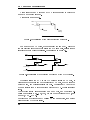
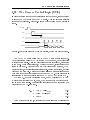
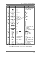
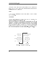
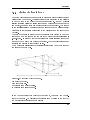
1
Contents
1 OBC Hardware documentation
6
1.1
Word abbreviation
. . . . . . . . . . . . . . . . . . . . . . . .
6
1.2
Determination of OBC HW functions . . . . . . . . . . . . . .
7
1.3
Overview of Cubesat hardware architecture . . . . . . . . . . .
7
1.4
Choice of components . . . . . . . . . . . . . . . . . . . . . . .
9
1.4.1
The temperature
. . . . . . . . . . . . . . . . . . . . .
9
1.4.2
Power consumption . . . . . . . . . . . . . . . . . . . .
9
1.4.3
Radiation
1.4.4
Size
1.4.5
Availability
1.5
. . . . . . . . . . . . . . . . . . . . . . . . .
10
. . . . . . . . . . . . . . . . . . . . . . . . . . . .
10
. . . . . . . . . . . . . . . . . . . . . . . .
Choice of component parts.
10
. . . . . . . . . . . . . . . . . . .
10
1.5.1
MCU . . . . . . . . . . . . . . . . . . . . . . . . . . . .
11
1.5.2
RAM . . . . . . . . . . . . . . . . . . . . . . . . . . . .
11
1.5.3
ROM/PROM/Flash memory
. . . . . . . . . . . . . .
11
1.5.4
Logic . . . . . . . . . . . . . . . . . . . . . . . . . . . .
12
1.6
Designing PCB
. . . . . . . . . . . . . . . . . . . . . . . . . .
12
1.7
Basic conguration of the MCU . . . . . . . . . . . . . . . . .
13
1.8
Memory management by the MCU
. . . . . . . . . . . . . . .
14
1.8.1
Byte access to memory . . . . . . . . . . . . . . . . . .
14
1.8.2
Decoding system
16
1.9
. . . . . . . . . . . . . . . . . . . . .
Controlling the Flash memory in the OBC
. . . . . . . . . . .
20
1.9.1
Boot strap programming . . . . . . . . . . . . . . . . .
20
1.9.2
Software controlled programming
20
1.9.3
Low level algorithm for ash/burn ROM
. . . . . . . . . . . .
. . . . . . . .
22
1.10 The Camera Control Logic (CCL) . . . . . . . . . . . . . . . .
25
1.11 Bus arbitration while storing data in RAM . . . . . . . . . . .
31
1.12 Hardware conguration . . . . . . . . . . . . . . . . . . . . . .
34
1.13 Power budget
. . . . . . . . . . . . . . . . . . . . . . . . . . .
35
1.14 Weight budget . . . . . . . . . . . . . . . . . . . . . . . . . . .
37
1.15 Physical connections of the C161PI
38
. . . . . . . . . . . . . . .
1
CONTENTS
1.16 System Block Diagram . . . . . . . . . . . . . . . . . . . . . .
40
1.17 Diagrams of the OBC . . . . . . . . . . . . . . . . . . . . . . .
41
1.17.1 Main MCU connections
. . . . . . . . . . . . . . . . .
44
1.17.2 RAM banks . . . . . . . . . . . . . . . . . . . . . . . .
45
1.17.3 ROM banks . . . . . . . . . . . . . . . . . . . . . . . .
46
1.17.4 DCL, CCL, counter etc.
47
. . . . . . . . . . . . . . . . .
2 Cubesat Internal I2 C-Bus
2.1
49
2
I C characteristic . . . . . . . . . . . . . . . . . . . . . . . . .
2
2.2
I C Protocol . . . . . . . . . . . . . . . . . . . . . . . . . . . .
52
2.3
Communication: . . . . . . . . . . . . . . . . . . . . . . . . . .
55
2.4
2
Write data to slave over I C bus . . . . . . . . . . . . . . . . .
2
2.5
Conducting housekeeping from a slave over the I C bus . . . .
2.6
Reading from a slave over the I C bus
2
. . . . . . . . . . . . .
3 Software functions
3.1
3.2
58
59
60
64
OBC Bootsequence . . . . . . . . . . . . . . . . . . . . . . . .
65
3.1.1
Basic boot from PROM
66
3.1.2
Checking for new software
3.1.3
Verifying new software
3.1.4
Advanced boot
3.1.5
BootSelection-port
. . . . . . . . . . . . . . . . . . . .
67
3.1.6
Get temperature on the OBC and Camera . . . . . . .
68
3.1.7
Flash Memory and load new data . . . . . . . . . . . .
69
3.1.8
Verie stored data
. . . . . . . . . . . . . . . . . . . .
70
Hamming corection of 2 errors . . . . . . . . . . . . . . . . . .
72
3.2.1
Encoding
72
3.2.2
Decoding and corect
. . . . . . . . . . . . . . . . .
. . . . . . . . . . . . . . . .
66
. . . . . . . . . . . . . . . . . .
66
. . . . . . . . . . . . . . . . . . . . . .
66
. . . . . . . . . . . . . . . . . . . . . . . . .
. . . . . . . . . . . . . . . . . . .
4 FPGA
72
75
4.1
Choosing a FPGA
. . . . . . . . . . . . . . . . . . . . . . . .
75
4.2
Designing the FPGA . . . . . . . . . . . . . . . . . . . . . . .
76
5 Payload
80
5.1
Introduction . . . . . . . . . . . . . . . . . . . . . . . . . . . .
80
5.2
Preliminary research
80
5.3
Construction of the camera
5.4
2
49
. . . . . . . . . . . . . . . . . . . . . . .
. . . . . . . . . . . . . . . . . . .
83
5.3.1
Interfacing the cameraunit . . . . . . . . . . . . . . . .
84
5.3.2
Exposure
84
5.3.3
Robustness of camera.
. . . . . . . . . . . . . . . . . . . . . . . . .
Structure budget of camera.
. . . . . . . . . . . . . . . . . .
85
. . . . . . . . . . . . . . . . . . .
86
CONTENTS
5.5
5.6
Lens
. . . . . . . . . . . . . . . . . . . . . . . . . . . . . . . .
5.5.1
Designing the lens
5.5.2
Placing the lens in focus
. . . . . . . . . . . . . . . . . . . .
5.5.3
Dierent lenses
5.5.4
Structure budget of lens
86
86
. . . . . . . . . . . . . . . . .
87
. . . . . . . . . . . . . . . . . . . . . .
88
. . . . . . . . . . . . . . . . .
90
Structure between camera and lens. . . . . . . . . . . . . . . .
90
I Appendix
91
A I2 C houskeeping
93
B I2 C read structure
95
C I2 C write structure
96
D OBC software structure
97
3
CONTENTS
Introduction
This document has been prepared by group 732.
It's purpose is to docu-
ment the design of the hardware to the On Board Computer system (OBC)
of the Cubesat. This document contains the detailed plans on how to build
the hardware, and also algorithms for the driver software.
4
OBC Hardware
Description:
This document describes how the OBC has been designed.
First an introduction is made to what is do be done, then requirements for
the OBC is investigated. A description of how components were chosen is
included hereafter.
The design includes besides the hardware of the com-
puter system, also address decoding mechanism, communication with payload which includes DMA for this and also hardware level descriptions on
several special features like ashing memory and taking picture.
Responsible group: pro 732, [email protected]
Date: 19.12.01
Rev.: 1.0
File name: OBC_design.pdf
Path: http://cubesat.auc.dk/documentation/OBC_design.pdf
Chapter 1
OBC Hardware documentation
1.1 Word abbreviation
ACS
Attitude Control System
CCL
Camera Control Unit
CS
Chip Select
BHE
Byte High Enable
MCU
Micro Controller Unit
NMI
Non Maskerable Interrupt
DCL
Decoding Control Logic
2
I C
LB
Interconnected Integrated Circuit
Lower Byte
OBC
On Board Computer
OS
Operating System
OTP
One Time Programmable
PROM
Programmable ROM
PSU
Power Supply Unit
RAM
Random Access Memory
ROM
Read Only Memory
UB
Upper byte
PCB
Printed circuit Board
DMA
Direct Memory Access
CDH
Control Data Handling
Table 1.1: List of words.
6
OBC Hardware documentation
1.2 Determination of OBC HW functions
In order to desing the HW (hardware) of the OBC (On Board Computer), it
is vital to determine its HW functions. The OBC HW consists of a minimum
2
computer system; a main processor, RAM, PROM, ash memory, I C bus
interface and external logic to control the memory modules and the camera.
The main function of the OBC HW is to create a physical platform for the
data handling system and ACS (Attitude Control System), is also to create
an interface to the other subsystems in the satellite.
The OBC hardware
2
should, beside being capable of handling the I C bus, also be capable of :
1. Reading and writing to RAM (4MB).
2. Read PROM and read/write to ash memory (256kB).
3. Addressing and decoding for selection of chips.
4. Bus arbitration on parallel bus, when grabbing data from camera.
5. Automatic reset of MCU if latchup or other single upset event has
stopped MCU.
1.3 Overview of Cubesat hardware architecture
Before explaining how the OBC works in detail, an overview of the hardware
architecture of the Cubesat is explained. A simplied model can be seen in
gure 1.1.
As it can be seen, the OBC hardware consists of the main MCU, PROM
(holding the basic program), Flash ROM (holding updated software) and
RAM (stack, picture etc.). Besides that it also contains logic to control the
memory, that is, chip selecting, timing signals etc. This is done in cooperation
with the CCL (Camera Control Logic), because the camera needs DMA
(Direct Memory Access) to RAM. The reason for this, is because data from
camera comes out in a stream, so timing and hardware DMA is required,
which is done by the CCL. This is actually not a part of the OBC, but since
it works closely together with the decoding logic, it has been implemented in
the same chips as this.
The external parts, as PSU (Power Supply Unit), Communication Unit etc.
2
has been connected via the I C bus.
This makes it easy for testing on a
PC later on. The communication unit, has also been connected to the main
MCU through a special communication bus. This is not explained further in
this document. For programming, both during developing phase and in the
7
OBC Hardware documentation
PC
RS232
OBC
Com.Bus
Comm. unit
I2C
A/D bus
PROM
ACS
MCU
C161PI
Flash
memory
PSU
Decoding Logic
(DCL)
RAM
Banks
Control bus
Payload
Figure 1.1:
8
Camera Control Logic
(CCL)
Overview of the architecture of the hardware in Cubesat.
OBC Hardware documentation
end phase, a serial interface has been implemented to a PC, via the RS232
serial interface.
1.4 Choice of components
This section describes the considerations we have made when choosing components for the on board computer. These components are the MCU, external memory and control logic.
Since space is a rough environment we have to select components capable
of withstanding radiation bombardment, out gassing and extreme changes in
temperature. This document describes the demands for each part and how
they are met.
1.4.1 The temperature
The dierence between cold (shade) and warm (illuminated) is very large
when not protected by the atmosphere (app. between -40 and 80
Æ C). There-
fore we have to choose components capable of working in a wide temperature
range. An advantage (when in shade) is that the only way the components
get chilled is by radiation. Since heat radiation is a slow heat conductor and
the components generate heat them self we do not expect that the components will be exposed to a rapid temperature change when moving into shade.
2
When illuminated the satellite will be exposed to 1300W/m
from the sun.
We expect the temperature on the sides of the satellite that faces the sun
Æ
to be app. 80
C. Inside the satellite temperature changes will be consider-
ably slower, because of internal mechanical structures, but it still have to be
taken into consideration. We have therefore limited the components to those
qualifying for industrial temperatures (-40-85
Æ
C).
1.4.2 Power consumption
Because of the limited amount of power available (<500mW5V) to the OBC
the power consumption of each component has to be taken into consideration.
Since the power consumption, in general, follows the frequency and we only
need to run the MCU at 12,5Mhz when the picture is taken, we will decrease
the frequency of the OBC when not taking a picture. We have also considered
using 3.3V components because of the lower power consumption but we had
to give up on the idea. A system based on 3.3V components would be more
sensitivity to noise and it has shown that it is practically impossible to nd
these components capable of industrial temperatures.
9
OBC Hardware documentation
1.4.3 Radiation
When not protected by Earths magnetic eld the satellite will be exposed to
high level of radiation. When electronics is exposed to radiation tree things
will happen:
Slowly the chip will degrade until nally not working.
Bit errors occurring when a bit ips.
Latch up resulting in a short circuit.
Since it is extremily expensive to buy special radiation hardened electronic
parts we have chosen to solve the radiation problem in a dierent way. By
using code correction (e.g. Hamming) and outer protection (e.g. metal protection) we minimize the amount of problems due to radiation without the
cost of special space approved components.
Further some technology are
preferable to others for example CMOS/HCMOS seems to be able to withstand radiation for a long period of time.
1.4.4 Size
Since we are limited in weight and volume we will try to use compact SMD
components.
1.4.5 Availability
Obtaining components with industrial specication in small numbers has
turned out to be dicult. There for we are using standard components during
the designing and development phase.
When construction the engineering
model and the ight model we are going to exchange all the components
with industrial components.
1.5 Choice of component parts.
When selecting the components it was needed to do some compromises. The
most important demands was the extended temperature ranges all parts meet
these demand. If all parts could work at a 3.3V power line the power consumption would bee smaller but this was not possible to get every part compatible whit 3.3V. In stead of the power voltages is 5V an then the MCU
frequency is decreased and only when the picture is taken the frequency is
set to 12,5MHz. Its all most impossible to get particular radiation hardened
10
OBC Hardware documentation
components by the distributors so we have to do other things to meet the
radiation problem. There might be a problem whit erasable memory units
like EEPROM etc in radiation environment since this will be erased by time.
Therefor there must be a non erasable ROM on bored satellite. We have not
done other hardware precations to avoid radiation problem. Almost all parts
are available as SMD components so that's what we have selected.
1.5.1 MCU
The MCU will be running most of the time and it is therefore especially important to limit the power consumption here. This is done by choosing a low
power MCU with the option of saving even more power by lowering the frequency. Beside low power consumption it is necessary that the MCU support
2
a large amount of memory and has an I C hardware bus interface. Besides
this we would like a couple of A/D-converters (for thermal measurement e.g.)
1.5.2 RAM
It has been particularly dicult nding RAM with industrial specications
and that is why we ended up using 8 modules of each 512kb. Since RAM
is especially sensitive to radiation we have to take special care.
We are
planning to deal with this problem by protecting the RAM modules with a
metal reinforcement and implementing an error correcting code. In the end
we have decided to use standard static RAM with industrial specications.
A major compromise was made here, since the found RAM consumes a lot
of power compared to all other components found. The major reason why
the clock frequency is lowered, is because of the RAM's since it consumes
55mW/MHz.
1.5.3 ROM/PROM/Flash memory
The boot software is going to be placed in a memory device capable of storing
data even if powered down.
We have chosen to use ash memory for this
task because it enables us to upload new software to the satellite. Since this
type of memory might be exposed to bit ips due to radiation we are going
to implement the original software in a PROM. Since PROM is one time
programmable (fused) its very dicult for it to be corrupted in space.
11
OBC Hardware documentation
1.5.4 Logic
On basis of recommendations from ESA and Terma we have decided to use
an FPGA (fused based) as programmable logic. This logic is going to ensure
RAM chip select. This has the advantage of saving power compared to using
PEEL and counters for CCL and DCL (see later in document).
1.6 Designing PCB
Like the other parts in the AAU CubeSat the print has to work in space
and therefore the material has to be taken into consideration when choosing.
As mentioned before, space is a vacuum environment where the temperature
vary between -40 and 85 Celsius degrees. Furthermore radiation will aect
the print board so it is not only a question to get the right material, but also
to make it radiation protected.
Before making the nal print, it has been decided to make a prototype print
in order to verify that the electronic circuits works properly. Therefore the
prototype print is not going to fulll the demands for space described above.
To verify that the electronic works properly the print has to consist of only
two layers in order to measure all points in the circuit.
The nal print is
possibly going to consist of more than two layers if all the wires are going
to be on one print, which has the size of approximately 90x90mm to t the
CubeSat.
At Aalborg University at the department of Telecommunication, they are
able make a print with two layers and a minimum width constraint of 0.3mm.
With this size it is impossible to make a PCB on a square of 90x90mm as it
has to be on the nal print, but for the test print, this is acceptable. Therefore the prototype is made at Aalborg University.
To make the print layout, the program Design Explorer 99 SE from Protel
is used. It has a trial period for 30 days, so the print board is nish within
that period of time. Things like redundancy and radiation protection is important, but the size of circuit we are working with, has certain diculties in
tting a large print board. So there is no room for hardware redundancy on
the prototype print board and as regarding radiation protection, we use the
rules Protel has build in when making the print. Protel could make a print
board at the square size of 150x200mm.
When the circuit on the prototype print board has been tested completely, the
12
OBC Hardware documentation
nal print is going to be made by the company GPV. They have the facility
to make a print board, which fulll the demands for industrial specication
described above. Only a vacuum test is needed to ensure that the PCB does
not degass in space. From Design Explorer 99 SE it is possibly to make the
print-board-les, which GPV can make print from. After GPV has made the
nal print we hope to get Terma to mount the components on the board, so
it is ensured that it is done the right way.
1.7 Basic conguration of the MCU
The Inneon C161PI can be congured in many ways, but it has been chosen
to use the following conguration :
Base oscillator frequency is chosen to 5MHz. This is normal operation
frequency, but while taking a picture 12,5MHz is used.
Databus is pure 16 bit, which takes up port 0
Addressbus is set to 20 bit, which means it can see blocks of 1Mb. How
it handles the 4Mb needed for the image is explained later.
For uploading it has been chosen to use the ASC0 (Serial Channel 0)
as default channel. This is explained later.
2
As I C interface, it has been chosen to select Line 1 with 7 bit addressing
mode, and the MCU as master.
Port 5 uses all its analog inputs for temperature sensors connected to
components within the OBC. This is for housekeeping, and temperature
warnings/failures etc. inside the OBC system.
Figure 1.24 in the end of this document, there is detailed block diagram
of the OBC HW, and how it is connected.
13
OBC Hardware documentation
1.8 Memory management by the MCU
Description of memory
The C161PI addresses its memory linearly, and can address up to 16MB. The
main memory of the OBC consists of several types. The two major types,
are internal and external memory.
The on chip memory consists of RAM only, which are split into two types:
1kb IRAM (Internal RAM) and 2kb XRAM (External RAM). IRAM is RAM
that lies next to the CPU, and is therefore extremely fast, and therefore it
is used as stack for the CDH. XRAM is RAM that lies on the same sillicium
chip, but has been put on the external address/databus which means that
the cpu accesses it as if it where ordinary external RAM. It is often used for
holding variables. The gain of using XRAM, is only speed, because it resides
on the same sillicium chip as the rest of the MCU.
The external memory is normal RAM, ROM and other peripherals mapped
onto the memory map.
Memory map of the system
It is chosen to store the image from the camera in RAM. Since 4Mb is needed
for holding the image, at least 8 chips must be used when each holds 512kb.
Besides RAM, the MCU also have at least 256kb of PROM for holding the
software. Beside this, it has been decided to implement extra 256kb of ash
memory above the PROM in order to be able to update application software
later on. This gives the following memory map shown in gure 1.2.
Due to easy implementation of the camera later on, it is chosen to use
the upper segment 8 as User RAM. The
CS
signals that selects individually
two segments at a time, are generated by the microcontroller. The C161PI
oers the opertunity to map 5 chipselects onto its memorymap.
This has
the advantage that, once programmed, it becomes transparent to the user,
hence the chip selecting requires much less external hardware. Signal
CS 0 is
always low whenever the other signals are not set low, which means that if
an error occurs and a read or write function is performed on addressed above
0x47FFFF, an illegal bus trap will happend, which software must take care of.
1.8.1 Byte access to memory
The data bus is 16 bit wide, while the address bus is 20 bit wide.
This
means that the MCU can address a whole segment directly at a time. This
also means that decoding each RAM chip is much more simple, which is
14
OBC Hardware documentation
Segment 8 (512kb)
User RAM
CS4
0x47FFFF
0x400000
Segment 7 (512kb)
0x380000
Segment 6 (512kb)
0x300000
CS3
Segment 5 (512kb)
0x280000
Segment 4 (512kb)
0x200000
CS2
Segment 3 (512kb)
0x180000
Segment 2 (512kb)
0x100000
CS1
Segment 1 (512kb)
0x080000
Flash memory (256kb)
0x040000
CS0
PROM (256kb)
0x000000
Figure 1.2:
Memory map of the C161PI main MCU
15
OBC Hardware documentation
described later in this section.
Since the RAM is 16 bit accessible it can cause a lot of wasted space if byte
access is required. The chosen RAM has a possibility to address byte wise,
and also the MCU supports this method on a 16 bit data bus. The RAM has
two pins to enable upper and lower byte, and if both pins are low, a whole
word is read. These pins are called
called
UB and LB .
The MCU has a special pin
BHE that enables the upper byte, when necessary.
Together with A0,
this makes it possible to get a exible byte access, without to much logic.
A0 enables the lower byte, and
BHE
enables the upper byte. This means
that words always are written on even byte addresses.
PROM and ash memory is done nearly the same way, but since these devices
are only 8 bit, a device is selected to hold the upper byte, and another device
holds the lower byte.
The result is, that for the MCU, it looks if the two
devices were one with the same capabilities as the RAM.
Since the camera returns 10 bit data, these will be stored as words in RAM.
Therefore when taking a picture, it will be necessary to enable both upper
and lower byte. This means that the logic shown in gure 1.3 is needed to
control
LB
and
UB
on RAM.
A0
LB
Word
Enable
BHE
Figure 1.3:
Signal
UB
Byte access control, including word enable from CCL.
Word Enable
is explained later.
is created from CCL (Camera Control Logic), which
This signal, of course, enables both bytes during data
transfer.
1.8.2 Decoding system
Determination of CS window
The register that programs the chip select lines are build up like shown in
table 1.4.
The address start bit eld, controls the upper 12 address bit, of where
the
CS
should be active. The lower four bits sets the length of the memory
window where the signal is active. For further information please read the
16
OBC Hardware documentation
Bit field
15
4 3
Start address
0
Length
Figure 1.4: The register ADDRSL that controls
CS
windowing
user manual for the C161PI, where other features with this mapping methods
are explained in details.
Chip selection within CS window
Since A0 is used for determination of low byte access, the address lines from
the MCU to RAM starts from A1-A18, and for PROM/ash memory A1-A17.
RAM has 18 bit address bus (A0-A17), which leaves 1 bit (A19) to determine
which chip is to be selected within the CS window. For both ROM types, the
chip within its CS window, is selected by A18. If, for instance, ash memory
CS 0 goes low, and A18 on the address bus goes high.
is to be selected, then
These two signals leads to the following boolean equation, that selects the
RAM chip (remember that chip select on any chip is always active low)
F lashmemory = CS 0 + A18
(1.1)
and for PROM
P ROM
= CS 0 + A18
(1.2)
By inspection in a truth table, it can be shown that only an OR gate and
a XNOR gate is neede to decode. The truth table is shown in table 1.2
CS1
A18
Gate
PROM
CS0
Gate
Flash memory
0
0
OR
0
0
XNOR
1
0
1
OR
1
0
XNOR
0
1
0
OR
1
1
XNOR
1
1
1
OR
1
1
XNOR
1
Table 1.2:
Truth table for decoding address signals.
17
OBC Hardware documentation
This means that an OR gate and a XNOR gate are needed to decode the
memory map for each segment.
This is shown in gure 1.5.
CS0
A18
CS
CS
FLash
memory
PROM
CS Window
Figure 1.5:
Realisation of the general decoding mechanism.
For most of the RAM chips, it works nearly the same way.
Since the
camera grabbing logic has to chip select the RAM's as well, a slight change
is introduced with these chip selects. This is shown in gure 1.6.
CS1
A19
CS
Camera seg1
CSseg1
CSseg2
CS
Camera seg2
Figure 1.6:
Realisation of the decoding mechanism of the RAM circuits.
Whenever either the MCU or the CCL tries to access a RAM chip, it
brings one of the inputs low to the respective AND gate, which makes the
output go low, and therefore selects the chip. The signals
x
CS Camera Seg
comes directly from a decoder system within the CCL. This is explained
later.
The decoding system is implemented on a PEEL chip, and the system requires 5 input lines (CS0,..,CS4,A18,A19) and 11 output lines (PROM,ash
memory,RAM1,..RAM8).
Reading from a device is done by pulling
will be enabled by the chip select.
18
OE
low on all chips, then output
OBC Hardware documentation
Writing is done the same way, just with the
memory also utilizes the
WR
signal.
Writing to ash
W R signal strobe, but in the end product, the OTP
only need writing once, and therefore a jumper will connect this line to the
PROM's write pin while programming.
Further time analysis is not performed for the MCU, since RAM and ROM
are much much faster than the MCU clock frequency, which will be 5-6MHz
(see section 1.13 for further details on this).
19
OBC Hardware documentation
1.9 Controlling the Flash memory in the OBC
The OBC must be able to ash/burn the program itself. This can be done
in two ways. The rst method, the boot strap programming, is done when
ashing/burning brand new software, and is only ment to be used during
development and when programming the PROM. The advantage is that it
is easy to use and you can programme the OBC directly from a PC through
a RS232 interface.
This, of course, requires extra components for voltage
adaption.
The second method is used when CDH is already running on the OBC. This
method is ment to be used, when Cubesat is in orbit and new software is
required.
1.9.1 Boot strap programming
Boot strap programming is an already build in feature in the C161PI. To
enter this mode, it requires an external pull down on P0L.4 during a reset.
This is, for simplicity done by a jumper and a resistor.
Besides this, a
serial connection to a PC is done through the MCU's asynchronous channel
0 (ASC0). This channel must be connected to a MAX232 device, in order to
ensure RS232 voltage levels.
From here a program can control the programming. After reset a 32 byte
long boot strap loader is loaded into the memory of the MCU. This loader
now handles the byte writing to the ash memory. When done, a reset can
be performed without the jumper on P0L.4, and the program will run, if
successfully ashed/burned. A sequence diagram for inline programming is
shown in gure 1.7
As it can bee seen from the gure, there's a lot of things happening
automatic, which means that with a minimum of eort the ROM can be
programmed. For security reason a jumper can be used to wire the WE pin
on the PROM while burning the system software. In this way, it is ensured,
that reprogramming of try of reprogramming PROM (since this may cause
errors) only is done when it is intended. The WE pin, should therefore be
tied high by a resistor, when not used.
1.9.2 Software controlled programming
As a way to secure properly working software it may be needed to upload
new application software. The system will in its boot sequence look if any
application software is located in the ash memory. If yes, the application
will be started from there, other vise it will run the standard modules from
20
OBC Hardware documentation
First level bootstraping
User initiates master reset, and holds
P0.4 low during reset(via jumper).
MCU C161PI enters Bootstrap mode
and awaits data on ASC0
PC sends a zero byte, with 1 start and
1 stop bit at the serial channel
MCU receives zero byte, and
synchronizes its baud rate generator
Not finished
MCU transmits a config code
PC/User sends bootload code
MCU recieves, and puts code in spec.
boot RAM
After finished, MCU runs bootstrap
code
Not finished
Fetch code on ASC0 from PC
Flash/copy memory with word
and increas address counter
Check if finished
Acknowledge and reset MCU
Second level bootstrapping
Figure 1.7:
Bootstrap sequence for ashing/burning software.
21
OBC Hardware documentation
the PROM.
The software controlled reprogramming method is to run a small program
from XRAM, that moves data uploaded from ground, to the Flash memory.
This has the advantage that new program data, is protected by the already
dened protocols.
Recieve data from ground
Copy data to RAM
Done by driver
Copy flash program to XRAM
Flash memory
Wait
Inform PSU of new SW
Reset when ready
Figure 1.8:
Procedure to ash memory. Procedure is called from CDH.
Figure 1.8 shows how the external software experiences ashing of the
memory. Receiving and copying program data is done by other, and when
ready the driver software will copy this into ROM. When done, the system
will go back in normal operation mode. During this process, the CDH will
be disabled, due to hard real time requirements from the hardware.
As a
requirement from the ash memory, no code must be executed from it, when
being ashed. Reading from the device, and therefore running code from it,
while trying to ash the device, is simply not possible.
1.9.3 Low level algorithm for ash/burn ROM
Actually no extra hardware is required in order to ash or burn the onboard
memory. The reason for this, lies in the way it is ashed. If the
R=W
line
from the MCU is connected to the WE pin on the ash memory, it can be
22
OBC Hardware documentation
written to nearly the same way as to RAM. The only dierence, is that,
for each byte written at a random address, three codes on both the address
and databus must be written, in order to enable the ash capability in the
ash memory. From the software programmers view, this looks like writing
a specic byte to a specic address in that memory area, before writing the
actual byte. This sequence can be seen in gure 1.9.
This algorithm also apply for the boot strap method, but since only 32
bytes of code is available, it may be necessary to skip the retry part, and just
reply to the PC that an error occurred. User must then try again. In table
1.3 it is shown how the command sequences are, for the M29F010B chip.
Command
Adr.1
Data1
Adr.2
Data2
Adr. 3
Data3
Adr.4
Data4
Program
555
AA
2AA
55
555
A0
PA
PD
Table 1.3: Command sequence for PROM. All numbers are in hex code.
PA is the program address, and PD is the program data. The only difference between the PROM and the Flash ROM lies in the address space.
When programming the PROM the addresses shown in the table is used.
When ashing the both lower and upper byte of the memory, addresses must
h
be added 40000
accordingly to the memory map. The data must also be
doubled in order to ash upper and lower device at the same time, i.e. write
0xAAAA at addr. 40555 for the rst part.
23
OBC Hardware documentation
Disable OS and
write erase commands to flash
memory
Wait
Fill buffer in XRAM (e.g. 64 words)
from RAM
Reset address
counter
Wait
Write Command Sequence
Write block erase
command
sequence
no
no
Write word to address
and increase addr. by one
Error bit
set?
Yes
No,
word OK
Buffer
empty?
Yes
Data
finish?
Inform PSU of new SW
Perform reset (by PSU)
Figure 1.9:
24
Low level procedure to ash ROM.
OBC Hardware documentation
1.10 The Camera Control Logic (CCL)
In order to design the hardware control logic for the camera, it is important
to look at how the camera and the RAM works. A timing sequence analysis
is done in the following. Figure 1.10 shows what happens when a picture is
taken.
TRIGGER
SYNC
tint
SOF
VCLK
trow
Databus
Row data
Figure 1.10:
The
Timing sequence of camera activity, during row transmission.
T RIGGER pin is pulled high by the MCU (only a pulse is needed).
A synchronization pulse (SYNC) is created by the camera, when this starts
to integrate the pixels. After the rst pixels has been integrated, data starts
to come out. A frame start signal, SOF(Start Of Frame), indicates that data
starts to come out.
After each row has been transmitted a signal, VCLK
(Vertical Clock), synchronizes all external logic. During this period, no valid
data is on the data bus. During data transmission an address counter must
be implemented in order to store the data in the RAM. Other glue logic is
also required to make it possible for both MCU and CCL to access RAM.
The time
trow
it takes to transfer a row, can be calculated by (MCLK
(Master Clock frequency) at 12,5MHz, vcwd means width of active window
and is set to 1280 pixels). The following equations has been taken from the
datasheet of the KAC-1310 chip.
trow
= (vcwd + 44) tMCLK
= (1280 + 44) 80ns
= 106s
(1.3)
(1.4)
(1.5)
With a total of 1024 rows, a total time of 106ms is needed to transfer the
25
OBC Hardware documentation
picture to RAM. The integration time (
tint ) is calculated by (cint is calculated
by the length of the active window plus three, i.e. 1024 + 3)
tint
= (cintdmin + 1) trow
= (1027 + 1) 109s
= 111ms
(1.6)
(1.7)
(1.8)
Hence, a total time of taking the picture, is approximately 217ms.
During row transmission, another synchronization is produced by the
camera.
Figure 1.11 shows these signals.
The
R=W
signal is the needed
signal for the RAM, in order to fetch the data on the bus.
MCLK
Databus
(column data)
1
2
3
R/W
twp tp
Figure 1.11:
sion.
Timing sequence of camera activity, during column transmis-
Since data is written to RAM on rising edge of the
R=W
signal, it is
necessary that this signal pulses with the right timing, accordingly to the
data being written onto the data bus from the camera.
requires that the signal is low for at least 50ns, i.e. that
means that the high period
tp can be max.
The RAM chips
twp >
50ns, this
30ns (with a MCLK at 12,5MHz).
Because of the RAM, it is required, as seen on the gure, that the
R=W
signal
is pulsed between a shift on the master clock. The generation of this signal
is done within the PEEL decoding chip, and a schematic of the gate logic is
shown in gure 1.12.
Since the
R=W
signal can be generated by the MCU also, it is necessary
to gate the to sources together. This is done, for simplicity, with and AND
gate in the end. If no units wants to write to any chips, both signals are held
high, and thus, the chips are set to read.
The
delay and switching circuit is done, both to delay the signal, for synchro-
nization with the MCLK signal, and to enable/disable whenever the pulses
are needed/not needed. This is done by OR'ing the delayed signal with the
26
OBC Hardware documentation
Delay 2
and swithing
Delay 1
Finish
S
Sync
R
SET
CLR
Q
Q
Word
Enable
Enable
Decoder
ACC
A
HCLK
B
C
R/W
VCLK
WR
(MCU)
Figure 1.12:
Gate logic for creating the R=W signal.
vertical line sync (VCLK) signal and a synchronization signal, resetted by the
cameras SYNC signal. This ensures that pulses only occurs when needed.
The
delay
is done in order to delay the HCLK (Horizontal Synchroniza-
tion signal), so the end pulse is shortened by the AND gate at point B, to
tp < 30ns, as required in the timing analysis.
To clock the address counter a delayed signal, ACC (Address Counter Clock)
is taken from point B as shown. The total signal timing diagram for the circuit is shown in gure 1.13.
HCLK
A
B, ACC
tcd
tWP
Done by
finish or VCLK signal
tp
C
MCLK
tmclk
Figure 1.13:
Timing sequence for the R=W pulse gate logic.
Depending on how fast the chosen PEEL chip is, additional or less delay
gates can be put in the dierent functionality boxes.
calculate the dierent times are as follows (where
The expressions to
td is the general propagation
delay in the PEEL, and n1,n2 is the number of delay gates)
27
OBC Hardware documentation
tp
twp
tcd
= 0; 5tmclk n td
= tmclk tp
= (n + n + 3) td
(1.9)
1
1
(1.10)
(1.11)
2
(1.12)
With a 15ns PEEL chip, the following can be calculated
= tmclk 0; 5tp = 80ns 0; 5 30ns = 65ns
= 65ns 3 15ns = 20ns
tcd
n1 + n2
(1.13)
(1.14)
(1.15)
This means that
n1
must consist of one gate, and
n2
should be non ex-
isting. With a delay of 15ns in the rst block, the pulse width (
twp) on 50ns.
tp )
will be
23ns, which is enough to ensure a write period (
tad ,
A total delay of 40ns (
address delay), counter delay is to be expected
from the counter, which means that the ACC must go high about 36ns after
the clock cycles positive edge.
tB ),
mately 30ns (
The signal at point B, is delayed approxi-
which means that a new valid address is available 70ns
after clock cycle start. This timing sequence is shown in gure 1.14.
HCLK
tB
tad
ACC (B)
Address
Bus
tVA
R/W
Figure 1.14:
Timing sequence for address counter.
A it can be seen, the address then changes shortly after
high.
that,
R=W
has gone
Since there are no requirements from RAM about this time, except
R=W
must go high before address change, there is no problem. To be
more precisely there are 10ns between
R=W
goes high, and address changes.
This should be enough to ensure proper writing. The following equations,
shows the calculations for this.
28
OBC Hardware documentation
tV A
tcd
= (n1 + 1) td + tad (n1 + n2 + 3) td
= 30ns + 40ns 60ns
= 10ns
(1.16)
(1.17)
(1.18)
In order to create address space for 1,3Mb that is needed for holding the
image, a 21 bit counter is needed. This is clocked by the ACC pulse. The
block diagram of this is shown in gure 1.15.
Finish
CCLR
CCE
Reset
OE
A19,A20,A21
3 bit
decoder
8 CS
Enable
decoder
20 bit
counter
18 bit address
(A1-A18)
ACC
Figure 1.15:
CU
Blockdiagram for creating address and chip select signals.
The rst 18 bit of the counter is used for creating the address on the
selected chip.
A18, A19 and A20 is connected to the PEEL chip and is
decoded internally to create a chip select for the RAM chips. A signal
nished
is put high as soon the image has been transferred. This is used to ensure
the
R=W
signal stays high, and to wake the MCU up by doing an external
hardware interrupt on pin EX7IN on the MCU.
The decoder is implemented in the PEEL chip as shown in gure 1.16.
The image takes up 1024x1280 (approximately 1.3 million) x 10 bit words,
which uses exactly 5 RAM blocks. This means that when the counter switches
to the 6th block, it will be nished transferring data. Hence, the
nish signal
is generated by the following equation
29
OBC Hardware documentation
CS
Camera seg7
CS7
CS
Camera seg6
CS6
CS
Camera seg5
CS5
A20
CS
Camera seg4
CS4
CS
Camera seg3
CS3
A19
CS
Camera seg2
CS2
A18
CS
Camera seg1
CS1
CS
Camera seg0
CS0
Enable
decoder
Figure 1.16:
30
Decoder for chip selecting when camera is active.
OBC Hardware documentation
finish = A20 + A19 + A18
(1.19)
which is easily implemented in the PEEL.
The inputs and outputs, shown in table 1.4 must be handled and created.
This can be archieved by 2 PEELs. By dividing the logic into two blocks,
this is easily done.
Inputs
Outputs
HCLK
-
WR
-
SYNC
-
VCLK
-
Usage
RW signal
Generation of RW signal
Synchronization of RW signal
Synchronization of RW signal
Generation of
-
RW
A17,A18,A19,A20
-
Chip select generation
CS0-5
-
Chip select generation (From MCU)
-
Enables upper and lower byte
-
CS0-9
Chip selects
-
Finish
EX07IN interrupt wake up signal to MCU
BHE
Table 1.4:
Enables RAM to write state
Required inputs and outputs on the PEELs.
1.11 Bus arbitration while storing data in RAM
When taking a picture of Denmark, and storing it into RAM, it is necessary
to arbitrate the MCU from the parrallel bus, since data and address signals
can interfere with the writing sequence. No matter how much time it takes
to store the data, the MCU must never write to either the data or address
bus in that time. Therefore it is necessary to put the MCU in idle mode,
while writing an image. It is also vital to put both address- and databus in
a high impedance mode in order not to short circuits the ports.
This is a tricky situation, because high impedancing the MCU from the bus
removes its possibility to fetch code data from ROM, and therefore to run
software at all. However since the MCU is equipped with XRAM that lies on
the same sillicium, and is accessed the same way as external memory, a tiny
code can be executed from here and do the trick. The procedure for taking
a picture is shown in gur 1.17.
31
OBC Hardware documentation
Done by CDH
Start task
Copy camera code to
XRAM
and run when ready
Done by code
Disable OS by disabling
GIE
High impedance
data/address bus
Activate camera
Go to idle mode
Done by hardware
Write image, and
generate HW interrupt
Done by code
Enable data/address bus
Enable OS, by enabling
GIE
Done by CDH
Wait state until next
image should be taken
Figure 1.17:
32
Bus arbitration procedure done by software on the MCU.
OBC Hardware documentation
While the MCU is in arbitration mode (idle mode), the picture storing
logic and the camera has the data/address bus for itself without any intervening from the MCU. When the image has been taken, a hardware interrupt
on EX7IN is created by the CCL. This awakens the MCU from idle mode.
By giving the EX7IN interruptlevel 0, it will only wake the MCU from Idle
mode. No interrupt service routine is needed.
33
OBC Hardware documentation
1.12 Hardware conguration
When resetting or setting power to the MCU, it must be hardware congured
to the system. This is done by several pins on port 0 (which is also the data
bus). External resistors on that port, or other units. Table 1.5 shows which
polarity the pins have, and what conguration this makes.
Pins
Values
Conguration
P0.0
1
Not in emulation mode
P0.1
1
Not in adapt mode
P0.5-2
1,1,1,1
Standard startup sequence
P0.7-6
1,0
16 bit data bus demultiplexed mode
P0.8
1
P0.10-9
1,1
P0.12-10
1,1
P0.15-13
0,0,0
RD
1
Standard use of
W R and BHE
Five chip select lines are necessary
Enable address lines A17, A18
Select PLL so
FCPU
= FOSC 2; 5
Enable watch dog timer
Table 1.5: Truth table for decoding address signals.
NB! Even though the base frequency is 5MHz times 2,5 (with PLL activated, which is 13MHz), software must lower this frequency when initialising.
This is purely to save power, and still being able to run at 12,5MHz when
taking a picture. It doesn't work the other way around!
Besides the hardware boot conguration, it is also necessary to initialize
the MCU hardware registers, so it works as supposed in this system. This
is done with a special initialization software that must be placed as the rst
code in the PROM.
34
OBC Hardware documentation
1.13 Power budget
Because the system has a limit on how much power it can consume, a power
budget must be made. In this section the total power dissipation is determined. The clock frequency can be used as a parameter to adjust the power.
During camera activity the clock must be about 12,5MHz.
Since not all
components has been chosen (the PLD or FPGA still has to be chosen) this
can inuence in the power budget.
As a starting point, data sheet for a
PEEL 22CV10A (15ns) has been chosen. With this in mind, the following
components, shown in table 1.6 is to be used.
Component
Name
Power consumption
1xRAM
TC554161AFT-70
1x55mW/MHz (active)
7xRAM
TC554161AFT-70
7x100 A (inactive)
2xROM
M29F010B
2x4mW/MHz* (active)
2xROM
M29F010B
2x0,325mW (inactive)
2xROM
M29F010B
2x100mW (Flash)
2xPLD
PEEL 22CV10A
2x75mW
1xMCU
C161PI
10mW/MHz
2xCounter
HC4020/24
0,8mW
1xCamera
KAC-1310
250mW
Table 1.6: Components accounted for in the OBC hardware.
*Note: This number has been derived with the assumption, that the power
dissipated for this circuit is linear dependent of the frequency, as the other
devices are.
It should also be noted that these numbers may vary with the temperature, and that these are based on typical values for the components. Based
on these gures, it is possible to sketch a power graph, based on the clock
frequency of the system. Since the components follow the main MCU's clock
frequency, this is the only parameter to control power consumption. This is
also software controllable, which makes it easy to save power, even during
ight. Figure 1.18 shows the power consumption in two situations, namely
in normal mode, and when ashing new software into ash memory.
With a simple calculation, by adding the power from active components
in camera mode, it can be shown from table 1.6 that the power consumed in
this mode is 1084mW. Since this mode only lasts for approximately 200ms
(see section 1.10 in this document) this should not be a problem for the
batteries to supply.
35
OBC Hardware documentation
2000
1800
Power consumption [mW]
1600
1400
1200
Flash
1000
Normal
800
600
400
200
0
5
10
15
20
Frequency [MHz]
Figure 1.18:
36
Power graph of OBC hardware in two situations.
25
OBC Hardware documentation
1.14 Weight budget
A weight budget must be setup, in order to determine the nal weight of the
OBC hardware.
This will come as soon we know exactly how the HW is going to be.
37
OBC Hardware documentation
1.15 Physical connections of the C161PI
This section describes how the pins will be connected on the C161PI. Table
1.7 shows this.
Pin
Name
Con
Note (Alt.func)
1-2
P5.2-3
NC
Analog Signals
3
T4EUD
NC
-
4
T2EUD
NC
-
5
Vss
GND
-
6
XTAL1
Crystal
See manual for con.
7
XTAL2
Crystal
-
8
Vdd
9-16
P3.0-7
+5V
-
Par.Data
Bus
to
Comm. unit
17
P3.8
NC
MRST
18
P3.9
NC
MTSR
19
P3.10
RS232 Transmit
TxD0 (ASC0)
20
P3.11
RS232 Recieve
RxD0 (ASC0)
21
P3.12
NC
BHE
22
P3.13
NC
SCLK
23
P3.15
Camera Clock in
fcpu
=
12,5MHz/5MHz
24
Vss
GND
-
25
Vdd
+5V
-
26
P4.0
Address Bus
A16
27
P4.1
Address Bus
A17
28
P4.2
Address Bus
A18
29
P4.3
Address Bus
A19
30
P4.4
NC
A20
31
P4.5
Write F.ROM1
-
32
P4.6
Write F.ROM2
-
33
34
35
38
RD
WR
READY
OE
W RMCU )
Con. on all chips
Peel (
-
NC
Ready from Ext.Mem.
OBC Hardware documentation
Pin
Name
Con
Note (Alt.func)
36
ALE
NC
Used only in muxed
bus mode, or as sync
EA
GND
External Access
38
Vss
GND
-
39
Vdd
+5V
-
40-47
P0L.0-P0.L7
Data bus
D0-D7
48
Vss
GND
-
49
Vdd
+5V
-
50-57
P0H.0-P0H.7
58
P1L0
59-65
P1L.1-P1L.7
66
37
Data bus
Address
D8-D15
0,
RAM
-
(LB), ROM (LB)
Address Bus
A1-A7
Vss
GND
-
67
Vdd
+5V
-
68-75
P1H.0-P1H.7
A8-A15
-
76
Vss
GND
-
77
Vdd
+5V
-
PSU
HW Reset, tied high
RST IN
78
RST OUT
NMI
79
80
by resistor
NC
Sync. Reset
NC
Non
CSx)
Maskable
Inter-
rupt
81-85
P6.0-4
PEEL (
CSx lines
86
P6.5
SDA1
I C data line 1
87
P6.6
SCL1
I C clock line 1
88
P6.7
NC
SDA2
89
P2.8
Comm. Interrupt
EX0IN
90-95
P2.9-14
Comm. unit
Comm.Control
2
2
Bus
(CCB)
96
P2.15
98
VAref
VaGND
99-100
P5.0-1
97
PEEL (nish)
Finish interrupt from
(CCL)
+5V
ADC reference voltage
GND
ADC ground
Temperature sensors
Analog Signals
Table 1.7: Pin connections on the C161PI microcontroller.
39
Par. port
PC
Decoding
logic
10
Control Bus
RS232
Serial
interface
CS 8
lines
WE
MAX232
PROM
128kb
Flash memory
128kb
Rx0Tx0
CS
R/W
WE
RAM Bank
4Mb
Camera
Control
logic
(CCL)
Sync
Signals
HCLK
8
Parallel bus interface
Master
Reset
Power
unit
PIC16
P3.10-11 RSTIN P6.0-4
+ others
ASC0
P3.15 Fcpu
2
ACS
Sensor/
Actuator
PIC16
EX7IN P2.15
P2.1-8
P3.0-7
I2C bus
Structure of OBC hardware.
Comm.
unit
PIC16xx
RD
Chip
Select
UB,LB
Serial port
HW Interface
16
P0
Data Bus
21
P0L.4
C161PI MCU
P1+
P4.0-3
Payload
Address bus
+5V
Varef
VDD
XTAL1
J1
Clk. IN
XTAL2
Analog
4
interface
(Temp. sensors for OBC)
P5.0-3
I2C
Interface 1
P6.5-6
EA
Vagnd
VSS
I2C
Interface
2
I2C bus
OBC Hardware documentation
Figure 1.19:
1.16 System Block Diagram
40
For test purposes
OBC Hardware documentation
1.17 Diagrams of the OBC
The OBC hardware diagrams, has been divided into four blocks, each contains details on how the OBC on AAU Cubesat works on hardware level.
The four blocks, and its bus connections, are shown in gure 1.20.
DCL
CCL
Counter
Address bus
Data bus
Control bus
I2C bus
Control Bus
Camera Control
C161PI
main MCU
Figure 1.20:
RAM
Banks
PROM
Flash memory
Dividing of OBC hardware diagrams.
The following tables contains valuable information when reading the diagrams.
Line nr.
Value
Meaning
0
IRQ
Interrupt request line from modem.
1
A0
Low bit address for modem.
2
A1
High address for modem.
3
PTT
Push to Talk
4
5
6
CE
RD
WR
Chip Enable for modem.
Read byte.
Write byte.
Table 1.8: Communication Control Bus (CCB[0..6]).
41
OBC Hardware documentation
Line nr.
0
1
2
3
4
5
6
7
Value
CS 0
CS 1
CS 2
CS 3
CS 4
RD
R=W
BHE
Meaning
Chip Select 0
Chip Select 1
Chip Select 2
Chip Select 3
Chip Select 4
Read enable
Write enable
Byte High Enable
Table 1.9: Control bus (CB[0..7]).
Line nr.
0
1
2
3
4
5
6
7
8
9
10
11
12
13
14
15
Value
P ROM LB
P ROM UB
F ROM LB
F ROM UB
RAM 1
RAM 2
RAM 3
RAM 4
RAM 5
RAM 6
RAM 7
RAM 8
RAM UB
RAM LB
R=W
RD
Meaning
PROM Low Byte enable
PROM High Byte enable
Flash ROM Low Byte enable
Flash ROM High Byte enable
RAM 1 enable
RAM 2 enable
RAM 3 enable
RAM 4 enable
RAM 5 enable
RAM 6 enable
RAM 7 enable
RAM 8 enable
RAM Upper byte enable
RAM Lower byte enable
Write enable strobe
Read enable strobe
Table 1.10: Control bus generated by decoding logic (DCL) (CS[0..15]).
42
OBC Hardware documentation
PEEL 1 in
I2 =A18
I3 =A19
I4 =A20
I5 =CS 1
I6 =CS 2
I7 =CS 3
I9 =CS 4
I10 =Enable Decoder
PEEL 1 out
O17 = RAM 1
O18 = RAM 2
O19 = RAM 3
O20 = RAM 4
O21 = RAM 5
O23 = RAM 6
O24 = RAM 7
O25 = RAM 8
O26 =Finish
PEEL 2 in
I2 =HCLK
I3 =SYNC
I4 =Finish
I5 =VCLK
I6 =HCLK
I7 = CS 0
I9 =A18
I10 =A0
I11 =BHE
PEEL 2 out
O17 = P ROM LB
O18 = P ROM UB
O19 = F ROM LB
O20 = F ROM UB
O21 = RAM LB
O23 = RAM UB
O24 = RW
O25 =Enable Decoder
Table 1.11: PEEL decoding logic I/O conguration pin assignments.
43
Connection of the MCU.
A
B
1
CON2
2
1
Power2
5V
2
C8
1uF
VDD
VCC
D[0..15]
R31
15k
CON3
3
2
1
ASC2
3
R32
15k
CON16
R33
15k
D4
R34
15k
JUMPER
2
1
CCB0
CCB1
CCB2
CCB3
CCB4
CCB5
CCB6
CBD7
CBD6
CBD5
CBD4
CBD3
CBD2
CBD1
CBD0
D5
D2
Bootstrap2
R35
15k
MCLK
30pF
C6
30pF
C5
D15
16
15
14
13
12
11
10
9
8
7
6
5
4
3
2
1
AN0
AN1
AN2
AN3
Trigger
CCLR
CCE
A[0..21]
R36
15k
VCC
R37
15k
CB[0..7]
VDD
CBD[0..7]
Y2
5MHz
CON6
6
5
4
3
2
1
Analog2
D14
R30
100k
4
R38
15k
VDD
CCB[0..6]
D6
ComBUS2
D13
4
CCB6
CBD0
CBD1
CBD2
CBD3
CBD4
CBD5
CBD6
CBD7
R39
15k
A16
A17
A18
A19
CB7
VCC
D11
3
CCB5
R40
15k
1
2
3
4
5
6
7
8
9
10
11
12
13
14
15
16
17
18
19
20
21
22
23
24
25
26
27
28
29
30
R26
100k
R27
100k
R28
100k
CCB4
EX7IN
P5.2/AN2
P5.3/AN3
P5.14/T4EUD
P5.15/T2EUD
VSS
XTAL1
XTAL2
VDD
P3.0/SCL0
P3.1/SDA0
P3.2/CAPIN
P3.3/T3OUT
P3.5/T3EUD
P3.5/T4IN
P3.6/T3IN
P3.7/T2IN
P3.8/MRST
P3.9/MTSR
P3.10/TxD0
P3.11/RxD0
P3.12/BHE/WRH
P3.13/SCLK
P3.15/CLKOUT/FOUT
VSS
VDD
P4.0/A16
P4.1/A17
P4.2/A18
P4.3/A19
P4.4/A20
CB5
CB6
C
2
D12
I2CSCL
I2CSDA
I2
CON3
5
1
2
3
C161PI
SAB C161PI
NMI
RSTOUT
RSTIN
VDD
VSS
P1H.7/A15
P1H.6/A14
P1H.5/A13
P1H.4/A12
P1H.3/A11
P1H.2/A10
P1H.1/A9
P1H.0/A8
VDD
VSS
P1L.7/A7
P1L.6/A6
P1L.5/A5
P1L.4/A4
P1L.3/A3
P1L.2/A2
P1L.1/A1
P1L.0/A0
P0H.7/AD15
P0H.6/AD14
P0H.5/AD13
P0H.4/AD12
P0H.3/AD11
P0H.2/AD10
P0H.1/AD9
R41
100k
5
Date:
File:
B
Size
Title
A7
A6
A5
A4
A3
A2
A1
A0
D15
D14
D13
D12
D11
D10
D9
A15
A14
A13
A12
A11
A10
A9
A8
VDD
VDD
80
79
78
77
76
75
74
73
72
71
70
69
68
67
66
65
64
63
62
61
60
59
58
57
56
55
54
53
52
51
Bootpins
CON2
VDD
VDD
1uF
C7
R29
54k
VDD
6
Revision
CON2
1
2
Reset2
6
13-Dec-2001
Sheet of
H:\P7\projekt\FinalGND\01gr732_v1.ddb Drawn By:
Number
OBC main MCU connection
D[0..15]
CB[0..7]
A[0..21]
U28
100k
R43 100k
R42
100
99
98
97
96
95
CCB6
94
CCB5
93
CCB4
92
CCB3
91
CCB2
90
CCB1
89
CCB0
88
87
86
85 CB4
84 CB3
83 CB2
82 CB1
81 CB0
P5.1/AN1
P5.0/AN0
V_(AGND)
V_(AREF)
P2.15/EX7IN
P2.14/EX6IN
P2.13/EX5IN
P2.12/EX4IN
P2.11/EX3IN
P2.10/EX2IN
P2.9/EX1IN
P2.8/EX0IN
P6.7/SDA2
P6.6/SCL1
P6.5/SDA1
P6.4/CS4
P6.3/CS3
P6.2/CS2
P6.1/CS1
P6.0/CS0
P4.5/A21
P4.6/A22
RD
WR/WRL
READY
ALE
EA
VSS
VDD
P0L.0/AD0
P0L.1/AD1
P0L.2/AD2
P0L.3/AD3
P0L.4/AD4
P0L.5/AD5
P0L.6/AD6
P0L.7/AD7
VSS
VDD
P0H.0/AD8
31
32
33
34
35
36
37
38
39
40
41
42
43
44
45
46
47
48
49
50
1
2
44
D0
D1
D2
D3
D4
D5
D6
D7
Figure 1.21:
D8
D
1
A
B
C
D
OBC Hardware documentation
1.17.1 Main MCU connections
D3
Figure 1.22:
A
B
C
D
1
5
4
3
2
54
53
52
51
33
32
31
30
29
27
26
25
24
23
13
12
43
15
42
41
14
22
1
A1
A2
A3
A4
A5
A6
A7
A8
A9
A10
A11
A12
A13
A14
A15
A16
A17
A18
CS4
CS12
CS13
CS14
CS15
A1
A2
A3
A4
A5
A6
A7
A8
A9
A10
A11
A12
A13
A14
A15
A16
A17
A18
CS8
CS12
CS13
CS14
CS15
1
5
4
3
2
54
53
52
51
33
32
31
30
29
27
26
25
24
23
13
12
43
15
42
41
14
22
1
DQ0
DQ1
DQ2
DQ3
DQ4
DQ5
DQ6
DQ7
DQ8
DQ9
DQ10
DQ11
DQ12
DQ13
DQ14
DQ15
VDD
VDD
VDD
VDD
GND
GND
GND
GND
NC
NC
NC
DQ0
DQ1
DQ2
DQ3
DQ4
DQ5
DQ6
DQ7
DQ8
DQ9
DQ10
DQ11
DQ12
DQ13
DQ14
DQ15
VDD
VDD
VDD
VDD
GND
GND
GND
GND
NC
NC
NC
TC554161FTL-85L
A0
A1
A2
A3
A4
A5
A6
A7
A8
A9
A10
A11
A12
A13
A14
A15
A16
A17
CE
UB
LB
R/W
OE
OP
OP
NC
NC
U19
TC554161FTL-85L
A0
A1
A2
A3
A4
A5
A6
A7
A8
A9
A10
A11
A12
A13
A14
A15
A16
A17
CE
UB
LB
R/W
OE
OP
OP
NC
NC
U15
49
48
45
44
39
38
35
34
21
20
17
16
11
10
7
6
8
36
47
19
9
37
46
18
28
40
50
49
48
45
44
39
38
35
34
21
20
17
16
11
10
7
6
8
36
47
19
9
37
46
18
28
40
50
D0
D1
D2
D3
D4
D5
D6
D7
D8
D9
D10
D11
D12
D13
D14
D15
D0
D1
D2
D3
D4
D5
D6
D7
D8
D9
D10
D11
D12
D13
D14
D15
VDD
VDD
2
2
A1 5
A2 4
A3 3
A4 2
A5 54
A6 53
A7 52
A8 51
A9 33
A10 32
A11 31
A12 30
A13 29
A14 27
A15 26
A16 25
A17 24
A18 23
CS9 13
CS1212
CS1343
CS1415
CS1542
41
14
22
1
A1 5
A2 4
A3 3
A4 2
A5 54
A6 53
A7 52
A8 51
A9 33
A10 32
A11 31
A12 30
A13 29
A14 27
A15 26
A16 25
A17 24
A18 23
CS5 13
CS1212
CS1343
CS1415
CS1542
41
14
22
1
DQ0
DQ1
DQ2
DQ3
DQ4
DQ5
DQ6
DQ7
DQ8
DQ9
DQ10
DQ11
DQ12
DQ13
DQ14
DQ15
VDD
VDD
VDD
VDD
GND
GND
GND
GND
NC
NC
NC
DQ0
DQ1
DQ2
DQ3
DQ4
DQ5
DQ6
DQ7
DQ8
DQ9
DQ10
DQ11
DQ12
DQ13
DQ14
DQ15
VDD
VDD
VDD
VDD
GND
GND
GND
GND
NC
NC
NC
TC554161FTL-85L
A0
A1
A2
A3
A4
A5
A6
A7
A8
A9
A10
A11
A12
A13
A14
A15
A16
A17
CE
UB
LB
R/W
OE
OP
OP
NC
NC
U20
TC554161FTL-85L
A0
A1
A2
A3
A4
A5
A6
A7
A8
A9
A10
A11
A12
A13
A14
A15
A16
A17
CE
UB
LB
R/W
OE
OP
OP
NC
NC
U16
49
48
45
44
39
38
35
34
21
20
17
16
11
10
7
6
8
36
47
19
9
37
46
18
28
40
50
49
48
45
44
39
38
35
34
21
20
17
16
11
10
7
6
8
36
47
19
9
37
46
18
28
40
50
D0
D1
D2
D3
D4
D5
D6
D7
D8
D9
D10
D11
D12
D13
D14
D15
D0
D1
D2
D3
D4
D5
D6
D7
D8
D9
D10
D11
D12
D13
D14
D15
VDD
VDD
3
3
5
4
3
2
54
53
52
51
33
32
31
30
29
27
26
25
24
23
13
12
43
15
42
41
14
22
1
A1
A2
A3
A4
A5
A6
A7
A8
A9
A10
A11
A12
A13
A14
A15
A16
A17
A18
CS10
CS12
CS13
CS14
CS15
A1
A2
A3
A4
A5
A6
A7
A8
A9
A10
A11
A12
A13
A14
A15
A16
A17
A18
CS6
CS12
CS13
CS14
CS15
5
4
3
2
54
53
52
51
33
32
31
30
29
27
26
25
24
23
13
12
43
15
42
41
14
22
1
DQ0
DQ1
DQ2
DQ3
DQ4
DQ5
DQ6
DQ7
DQ8
DQ9
DQ10
DQ11
DQ12
DQ13
DQ14
DQ15
VDD
VDD
VDD
VDD
GND
GND
GND
GND
NC
NC
NC
DQ0
DQ1
DQ2
DQ3
DQ4
DQ5
DQ6
DQ7
DQ8
DQ9
DQ10
DQ11
DQ12
DQ13
DQ14
DQ15
VDD
VDD
VDD
VDD
GND
GND
GND
GND
NC
NC
NC
TC554161FTL-85L
A0
A1
A2
A3
A4
A5
A6
A7
A8
A9
A10
A11
A12
A13
A14
A15
A16
A17
CE
UB
LB
R/W
OE
OP
OP
NC
NC
U21
TC554161FTL-85L
A0
A1
A2
A3
A4
A5
A6
A7
A8
A9
A10
A11
A12
A13
A14
A15
A16
A17
CE
UB
LB
R/W
OE
OP
OP
NC
NC
U17
49
48
45
44
39
38
35
34
21
20
17
16
11
10
7
6
8
36
47
19
9
37
46
18
28
40
50
49
48
45
44
39
38
35
34
21
20
17
16
11
10
7
6
8
36
47
19
9
37
46
18
28
40
50
D0
D1
D2
D3
D4
D5
D6
D7
D8
D9
D10
D11
D12
D13
D14
D15
D0
D1
D2
D3
D4
D5
D6
D7
D8
D9
D10
D11
D12
D13
D14
D15
4
4
VDD
VDD
5
4
3
2
54
53
52
51
33
32
31
30
29
27
26
25
24
23
13
12
43
15
42
41
14
22
1
A1
A2
A3
A4
A5
A6
A7
A8
A9
A10
A11
A12
A13
A14
A15
A16
A17
A18
CS11
CS12
CS13
CS14
CS15
A1
A2
A3
A4
A5
A6
A7
A8
A9
A10
A11
A12
A13
A14
A15
A16
A17
A18
CS7
CS12
CS13
CS14
CS15
5
4
3
2
54
53
52
51
33
32
31
30
29
27
26
25
24
23
13
12
43
15
42
41
14
22
1
DQ0
DQ1
DQ2
DQ3
DQ4
DQ5
DQ6
DQ7
DQ8
DQ9
DQ10
DQ11
DQ12
DQ13
DQ14
DQ15
VDD
VDD
VDD
VDD
GND
GND
GND
GND
NC
NC
NC
DQ0
DQ1
DQ2
DQ3
DQ4
DQ5
DQ6
DQ7
DQ8
DQ9
DQ10
DQ11
DQ12
DQ13
DQ14
DQ15
VDD
VDD
VDD
VDD
GND
GND
GND
GND
NC
NC
NC
TC554161FTL-85L
A0
A1
A2
A3
A4
A5
A6
A7
A8
A9
A10
A11
A12
A13
A14
A15
A16
A17
CE
UB
LB
R/W
OE
OP
OP
NC
NC
U22
TC554161FTL-85L
A0
A1
A2
A3
A4
A5
A6
A7
A8
A9
A10
A11
A12
A13
A14
A15
A16
A17
CE
UB
LB
R/W
OE
OP
OP
NC
NC
U18
49
48
45
44
39
38
35
34
21
20
17
16
11
10
7
6
8
36
47
19
9
37
46
18
28
40
50
5
49
48
45
44
39
38
35
34
21
20
17
16
11
10
7
6
8
36
47
19
9
37
46
18
28
40
50
5
Date:
File:
B
Size
Title
D0
D1
D2
D3
D4
D5
D6
D7
D8
D9
D10
D11
D12
D13
D14
D15
D0
D1
D2
D3
D4
D5
D6
D7
D8
D9
D10
D11
D12
D13
D14
D15
A[0..21]
CS[0..15]
D[0..15]
18-Dec-2001
H:\P7\projekt\FinalGND\01gr732_v1.ddb
Number
Memory banks 1-8
VDD
VDD
Sheet of
Drawn By:
6
A[0..21]
CS[0..15]
D[0..15]
6
Revision
A
B
C
D
OBC Hardware documentation
1.17.2 RAM banks
RAM banks.
45
46
Figure 1.23:
ROM banks.
A
B
C
D
1
1
2
A1
A2
A3
A4
A5
A6
A7
A8
A9
A10
A11
A12
A13
A14
A15
A16
A17
A1
A2
A3
A4
A5
A6
A7
A8
A9
A10
A11
A12
A13
A14
A15
A16
A17
2
20
19
18
17
16
15
14
13
3
2
31
1
12
4
5
11
10
20
19
18
17
16
15
14
13
3
2
31
1
12
4
5
11
10
M29F010B
A0
A1
A2
A3
A4
A5
A6
A7
A8
A9
A10
A11
A12
A13
A14
A15
A16
R24
M29F010B
A0
A1
A2
A3
A4
A5
A6
A7
A8
A9
A10
A11
A12
A13
A14
A15
A16
R22
LowerByte
NC
VCC
VSS
E
OE
W
D0
D1
D2
D3
D4
D5
D6
D7
UpperByte
NC
VCC
VSS
E
OE
W
D0
D1
D2
D3
D4
D5
D6
D7
6
8
24
30
32
7
21
22
23
25
26
27
28
29
6
8
24
30
32
7
21
22
23
25
26
27
28
29
D0
D1
D2
D3
D4
D5
D6
D7
D8
D9
D10
D11
D12
D13
D14
D15
CS0
CS15
CS14
CS1
CS15
CS14
3
VDD
3
VDD
A1
A2
A3
A4
A5
A6
A7
A8
A9
A10
A11
A12
A13
A14
A15
A16
A17
A1
A2
A3
A4
A5
A6
A7
A8
A9
A10
A11
A12
A13
A14
A15
A16
A17
20
19
18
17
16
15
14
13
3
2
31
1
12
4
5
11
10
20
19
18
17
16
15
14
13
3
2
31
1
12
4
5
11
10
M29F010B
A0
A1
A2
A3
A4
A5
A6
A7
A8
A9
A10
A11
A12
A13
A14
A15
A16
R25
M29F010B
A0
A1
A2
A3
A4
A5
A6
A7
A8
A9
A10
A11
A12
A13
A14
A15
A16
R23
LowerByte
NC
VCC
VSS
E
OE
W
D0
D1
D2
D3
D4
D5
D6
D7
UpperByte
NC
VCC
VSS
E
OE
W
D0
D1
D2
D3
D4
D5
D6
D7
6
8
24
30
32
7
21
22
23
25
26
27
28
29
6
8
24
30
32
7
21
22
23
25
26
27
28
29
4
CS2
CS15
CS14
D0
D1
D2
D3
D4
D5
D6
D7
D8
D9
D10
D11
D12
D13
D14
D15
4
CS3
CS15
CS14
VDD
CS[0..15]
D[0..15]
A[0..21]
VDD
D[0..15]
A[0..21]
CS[0..15]
5
5
Date:
File:
B
Size
Title
18-Dec-2001
H:\P7\projekt\FinalGND\01gr732_v1.ddb
Number
ROM Banks 1-4
Sheet of
Drawn By:
6
6
Revision
A
B
C
D
OBC Hardware documentation
1.17.3 ROM banks
A
B
1
16
8
9
10
11
12
13
14
16
8
9
10
11
12
13
14
16
8
HC590A
VCC
VSS
RCO
CCLR
CCLK
CCKEN
RCLK
OE
U25
HC590A
VCC
VSS
RCO
CCLR
CCLK
CCKEN
RCLK
OE
HC590A
U24
VCC
VSS
RCO
CCLR
CCLK
CCKEN
RCLK
OE
2
Q0
Q1
Q2
Q3
Q4
Q5
Q6
Q7
Q0
Q1
Q2
Q3
Q4
Q5
Q6
Q7
Q0
Q1
Q2
Q3
Q4
Q5
Q6
Q7
15
1
2
3
4
5
6
7
15
1
2
3
4
5
6
7
15
1
2
3
4
5
6
7
A17
A18
A19
A20
A21
A9
A10
A11
A12
A13
A14
A15
A16
A1
A2
A3
A4
A5
A6
A7
A8
CamEPROM
I2CSCL
I2CSDA
CameraCon
CON34
A[0..21]
VDD
CB[0..7]
D17
D16
U23
SensRst
9
10
11
12
13
14
Trigger
C
CCE
CCLR
VDD
3
A[0..21]
CB[0..7]
D15
D14
D13
D12
D
2
SYNC
HCLK
VCLK
D11
D10
D9
D8
Figure 1.24:
MCLK
CB5
A18
A0
CB7
CB6
CB0
CB4
En.Dec.
A19
A20
A21
CB1
CB2
CB3
1
2
3
4
5
6
7
8
9
10
11
12
13
14
1
2
3
4
5
6
7
8
9
10
11
12
13
14
4
3
4
VDD
VCC
I/O
I/O
I/O
I/O
I/O
NC
I/O
I/O
I/O
I/O
I/O
I
NC
VCC
I/O
I/O
I/O
I/O
I/O
NC
I/O
I/O
I/O
I/O
I/O
I
NC
D[0..15]
PEEL22CV10A
NC
I/CLK
I
I
I
I
I
NC
I
I
I
I
I
VSS
U27
PEEL22CV10A
NC
I/CLK
I
I
I
I
I
NC
I
I
I
I
I
VSS
U26
34
33
32
31
30
29
28
27
26
25
24
23
22
21
20
19
18
17
16
15
14
13
12
11
10
9
8
7
6
5
4
3
2
1
1
28
27
26
25
24
23
22
21
20
19
18
17
16
15
28
27
26
25
24
23
22
21
20
19
18
17
16
15
CS12
CS3
CS2
CS1
CS0
CS14
CS13
CS8
CS7
CS6
CS5
CS4
CS11
CS10
CS9
Finish
CS15
VDD
5
Finish
CS[0..15]
5
Date:
File:
B
Size
Title
18-Dec-2001
H:\P7\projekt\FinalGND\01gr732_v1.ddb
Number
Decoding and CCL logic
VDD
CS[0..15]
Sheet of
Drawn By:
6
6
Revision
A
B
C
D
OBC Hardware documentation
1.17.4 DCL, CCL, counter etc.
DeCoding Logic, Camera Control Logic, counter, etc.
47
2
Cubesat Internal I C-Bus
Description:
The purpose of this document is to describe the internal bus
2
on the Cubesat. The internal bus has been chosen to be the I C-bus Interconnected Integrated Circuit. The document will describe the purpose of
2
the I C and the design of a suitable Protocol for the data link layer.
Responsible group: pro 732, [email protected]
Date: 19.12.01
Rev.: 1
File name: OBC_design.pdf
Path: http://www.cubesat.auc.dk/dokumenter/OBC_design.pdf
Literature:
http://www-us.semiconductors.philips.com/i2c/facts/
Chapter 2
2
Cubesat Internal I C-Bus
2.1 I2C characteristic
In order to obtain communication between the dierent subsystems on the
2
2
AAU cubesat, the Philips I C bus has been selected. I C or Interconnected
Integrated Circuit was developed by Philips in 1992 it has now become the
world standard, and is currently implemented in over 1000 dierent ICs.
Here are some of the features of the I2 C-bus:
Only two bus lines are required; a serial dataline (SAD) and a serial
clock line (SCL).
Each device connected to the bus is software addressable by a unique
address and simple master/slave relationships exist at all times; masters can operate as master-transmitters or as master-receivers.
It s a true multi-master bus including collision detection and arbitration to prevent data corruption if two or more masters simultaneously
initiate data transfer.
Serial 8-bit oriented bi-directional data transfers can be made at up to
100 kbit/s in the Standard-mode, up to 400 kbit/s in the Fast-mode,
49
Cubesat Internal I2 C-Bus
or up to 3.4 Mbit/s in the High-speed mode.
On-chip ltering rejects spikes on the bus data line to preserve data
integrity.
Extremely low current consumption.
High noise immunity.
Wide supply voltage range.
Wide operating temperature range.
2
The I C-bus supports any IC fabrication process (NMOS, CMOS, bipolar).
Two wires, serial data (SDA) and serial clock (SCL), carry information between the devices connected to the bus. Each device is recognized by a unique
address (whether it's a microcontroller, LCD driver, memory or keyboard interface) and can operate as either a transmitter or receiver, depending on the
function of the device. Obviously a LCD driver is only a receiver, whereas
a memory can both receive and transmit data. In addition to transmitters
and receivers, devices can also be considered as masters or slaves when performing data transfers (see Table 2.1). A master is the device which initiates
a data transfer on the bus and generates the clock signals to permit that
transfer. At that time any device addressed is considered a slave.
2
The I C-bus is a multi-master bus.
This means that more than one de-
vice capable of controlling the bus can be connected to it. As masters are
usually micro-controllers, let s consider the case of a data transfer between
2
two microcontrollers connected to the I C-bus (see Fig.2.1).
50
Cubesat Internal I2 C-Bus
Term
DESCRIPTION
Transmitter
The device which sends data to the bus
Receiver
The device which receives data from the bus
Master
The device which initiates a transfer, generates clock
signal and terminates transfer.
Slave
The device addressed by a master
Multi-master
More than one master can attempt to control the bus at
the same time without corrupting the message
Arbitration
Procedure to ensure that, if more than one master simultaneously tries to control the bus, only one is allowed to
do so, and the winning message is not corrupted
Synchronization
Procedure to synchronize the clock signals of two or
more devices
Table 2.1:
Denition of I2 C-Bus terminology.
CUBESAT BUS structure
RAM/ROM
PAYLOAD
COM
OBC
OSSS−com
Microcontrtoller
Unit
Com. databus
Databus
C161PI
DEVITECH
ONBOARD
CAMERA
SDA
SCL
ACS
PSU
External
PC
Figure 2.1:
I2 C-Bus structure.
If two or more masters try to put information onto the bus, the rst to produce a 1 when the other produces a zero will lose the arbitration.
The
clock signals during arbitration are a synchronized combination of the clocks
generated by the masters using the wired-AND connection to the SCL line.
2
Generation of clock signals on the I C-bus is always the responsibility of
master devices; each master generates its own clock signals when transfer-
51
Cubesat Internal I2 C-Bus
ring data on the bus. Bus clock signals from a master can only be altered
when they are stretched by a slow-slave device holding-down the clock line,
or by another master when arbitration occurs.
The Cubesat structure consists internally of ve dierent modules (COM,
OBC, ACS, PSU and Payload). The last module on gure 1 is an external
PC which is used for testing and simulation of the system.
2.2 I2C Protocol
2
The I C protocol consists of the following.
Start:
The start condition is produced by a master, who wants to use the bus.
It is made by holding the SCL line high, while changing the SDA line from
high to low.
Address:
Address
Predefigned
Address
Figure 2.2:
Programable
address
R/W
Bit
I2 C-Bus address.
2
Every device on the I C-Bus has its own unique 7 bit address.
The rst
4 bit of the address is determined by the type of device connected to the
2
I C-Bus and is set by the manufacture of the IC. The last three bits are pro2
grammable, which allows 8 identical devices to be connected to the I C-Bus.
R/W:
Read/Write is set by the Master, and determines whether the master wants
to read from the slave or write to it. 1 for read and 0 for write.
Acknowledge:
52
Cubesat Internal I2 C-Bus
Header
No of data Packages
000xxxxx
0
001xxxxx
1
010xxxxx
2
011xxxxx
3
100xxxxx
4
101xxxxx
5
110xxxxx
6
111xxxxx
7
Table 2.2:
Number of data packages.
Data transfer with acknowledge is obligatory. The acknowledge-related clock
pulse is generated by the master.
The transmitter releases the SDA line
(HIGH) during the acknowledge clock pulse.
The receiver must pull down the SDA line during the acknowledge clock pulse
so that it remains stable LOW during the HIGH period of this clock pulse,
in order to conrm that it is willing to communicate.
Header: Length:
Header
Length
In Bytes
Module Number
Figure 2.3:
I2 C-header.
The rst three bits of the header determine how many data packages the
header will be followed by (up to 7 * 8 bit data packages) (see tabel:2.2).
Module:
The device module number.
E.g.
The PSU temp probe nr.
2 (2*8 bit
data) [00100010]. The total amount of modules you can address is
2 = 32
5
Data:
53
Cubesat Internal I2 C-Bus
The data on the SDA line must be stable during the HIGH period of the
clock. The HIGH or LOW state of the data line can only change when the
clock signal on the SCL line is LOW
Stop:
A LOW to HIGH transition on the SDA line while SCL is HIGH denes
a STOP condition.
Checksum:
The data package following the header is an 8 bit CRC Checksum.
The
checksum is calculated in the following way.
All the data packages and the header send in one transmission are added together, the 8 bit result of this calculation is the subtracted from [FFh], this
yields the CRC checksum. The sum of received data is added with the checksum. The result is now divided by [FFh] and the modulus of this calculation
indicates weather the transmitted data is corrupted. If the result is dierent
from 0 the data is corrupted and will be retransmitted. (see Tabel:2.4)
SEND DATA
[11111111]
(FFh)
−
(DATA)
RECIEVED DATA
(CRC)
+
[01101101]
[01101101]
[10110101]
[10110101]
+
+
=
(CRC)
[11011101]
=
[11011101]
(FFh)
[11111111]
DATA OK
Figure 2.4:
54
Calculation of checksum.
Cubesat Internal I2 C-Bus
Master communicating to slave
S
Slave address
R/W A
DATA
A
DATA
A/A P
A = Acknowledge (SDA LOW)
’0’ (write)
A = Not acknowledge (SAD HIGH)
S = START condition
From master to slave
P = STOP condition
From slave to master
Sr = Repeted START condition
A master reads a slave immediately after the first byte.
S
Slave address
R/W A
DATA
A
DATA
A
P
Combined format
S
Slave address
R/W A
DATA
A/A Sr
not shaded
because transfer
direction of data
and acknowledge bits
depends on R/W bits.
Figure 2.5:
Slave address
R/W A
DATA
A/A P
not shaded
because transfer
direction of data
and acknowledge bits
depends on R/W bits.
Raed or write
I2 C-Bus communication.
2.3 Communication:
Possible data transfer formats are: Master-transmitter transmits to slavereceiver. The transfer direction is not changed (see Fig.2.5).
Master reads slave immediately after rst byte (see Fig.2.5).
At the mo-
ment of the rst acknowledge, the master- transmitter becomes a masterreceiver and the slave-receiver becomes a slave-transmitter.
This rst ac-
knowledge is still generated by the slave. The STOP condition is generated
by the master, which has previously sent a not-acknowledge (A).
Combined format (see Fig.2.5). During a change of direction within a transfer, the START condition and the slave address are both repeated, but with
the R/W bit reversed. If a master receiver sends a repeated START condition, it has previously sent a not-acknowledge (A).
55
Cubesat Internal I2 C-Bus
NOTES:
1.Combined formats can be used, for example, to control a serial memory. During the rst data byte, the internal memory location has to
be written. After the START condition and slave address is repeated,
data can be transferred.
2.All decisions on auto-increment or decrement of previously accessed
memory locations etc. are taken by the designer of the device.
3.Each byte is followed by an acknowledgment bit as indicated by the
A or A blocks in the sequence.
I 2 C -bus
4.
compatible devices must reset their bus logic on receipt of
a START or repeated START condition such that they all anticipate
the sending of a slave address, even if these START conditions are not
positioned according to the proper format.
5.A START condition immediately followed by a STOP condition (void
message) is an illegal format.
Conducting housekeeping
When collecting housekeeping from the dierent units the master only needs
to address a unit and set the R/W condition to Read. The unit then delivers all its housekeeping data to the MCU. Each sensor on a unit is identied
by the module number transmitted in the header.
2
The funktion for collecting housekeeping is called I CHousekeeping().
order to work it needs 2 parameters
1. Unit
The name of the unit from where housekeeping is conducted
2. Datapointer
The stack pointer where the data will be stored
A practial eksamble
56
In
Cubesat Internal I2 C-Bus
2
void I CHousekeeping(int PSU, *datastak)
Controlling Units
When controlling a unit from the MCU, the MCU will of course have to
send data along with the address, header and checksum. In order to write
2
data to a unit the I CWrite() funktion is used.
A practial eksamble
2
void I CWrite(int PSU, CRCchecksum, header, *datapointer)
It is also possible to read data from a specik sensor in order to do this,
2
the funktion I CRead() is used.
A practial eksamble
2
void I CRead(int PSU, CRCchecksum, header, *datapointer)
2
Further information about the I C-bus can be found at.
http://www-us.semiconductors.philips.com/i2c/facts/
57
Cubesat Internal I2 C-Bus
2
The I C is supported by the MCU. This means that it is not necessary
2
to build complex external hardware to set up an I C interface.
The only
hardware needed is pull up resistors on the two bus lines.
2
The I C bus is
congured, monitored and controlled by setting and reading dierent internal
registers:
ICCFG, I C conguration register, this register enables the desired
2
2
2
I C bus ports. The MCU has two complete I C interfaces. Interface 1
is used in this project. The register also sets the bit rate for the bus.
2
The OBC I C bus uses 97.6 kb/s.
ICCON, I C control register, this register is used to operate the bus.
2
It selects between 7 and 10 bit addresses. In the project 7 bit addresses
are used. It sets the MCU to be the master of the bus, it indicates if
the MCU should be receiving or transmitting data and it controls how
the receiver buer generates interrupts.
ICADR, I C address register, this register holds the adress of the MCU
2
in case it is used as a slave.
ICST, I C status register, this register holds the current status of the
2
2
I C bus and indicates if an interrupt is pending
ICRTB, I C transmit and receive buer, the buer is 1 byte long. If it
2
is dened in the ICCON register the ICRTB automatically interrupts
when the MCU reads from/writes to it.
Some of the micro controllers implemented in the subsystems did not
support the REPEATED START command. The REPEATED START command is used when the OBC wishes to both read and write from a slave during
2
2
communication. This command is a vital part of the I C standard. The I C
protocol developed during the project therefore had to be modied.
2
Three dierent software modules used to communicate over the I C bus was
developed. The module algorithms have been illustrated using owcharts. In
the following sections these owcharts will be described.
2.4 Write data to slave over I2C bus
The algorithm shown in gure 2.6 is used when the master want to send data
to a slave.
2
First the operating system locks the access to the I C bus. This ensures that
58
Cubesat Internal I2 C-Bus
2
a program wanting to transmit on the I C bus do not overwrite a transmission already in progress.
operating system.
The locking of the bus is done internally in the
It sets up a semaphore (program) that blocks access to
the bus.
After blocking access to the bus, the status register is reset.
Next the in-
terrupt of the transmission buer is set up. The interrupt uses the MCUs
Peripheral Event Controller (PEC). PEC is a function that can move data
from one place in the memory map to another using only one clock cycle.
After setting up interrupts the header for the data and a checksum is calcu2
lated according to the I C protocol designed.
The algorithm then looks up the 7 bit hardware address according to the
subsystem the program wishes to transmit to.
This address is then placed in the transmission buer and sent to the slave.
As soon as the transmission has started the program breaks. When the address has been transmitted the buer generates an interrupt, beginning the
execution a new program. This program checks if there was an acknowledge
from a slave. If not it breaks and returns an error message. In case of acknowledge it places the rst byte of data that should be transmitted into the
data buer. When this is done it breaks. The PEC will then automatically
move the next byte into the transmission buer when the previous byte has
been sent. When all the data has been transmitted the PEC interrupts. The
new interrupt checks for an acknowledge from the slave.
It then frees the
bus, indicating to the slaves that the MCU is done, frees the semaphore so
another program can transmit and returns the status of the transmission.
The program writing to the slave should conduct a read command after each
write to see if the slave received the correct data, but this is optional in this
algorithm.
2.5 Conducting housekeeping from a slave over
the I2C bus
When the MCU wants to receive housekeeping from a subsystem it will be
done using the algorithm shown in gure 2.7.
As when writing data to
2
a unit as described above the algorithm rst locks access to the I C bus.
It then resets the control register and sets up and ordinary interrupt.
It
also transmits the address to the slave it wants to read from, breaks and
interrupts when this is done.
The interrupt routine checks to see if the
address was acknowledge by the slave. The MCU then switches into receiver
mode.
This can be seen from the slave so the slave immediately starts to
59
Cubesat Internal I2 C-Bus
send its housekeeping data.
The MCU uses a PEC routine to receive the
data. every time the transmission buer is full the data is moved from the
transmission buer and into a buer in the memory. When all the data except
the last byte has been recieved the PEC routine generates an interrupt. This
interrupt disables the automatic acknowledge generated from the MCU. This
2
is done to generate a not-acknowledge according to the I C standard. The
MCU then disables the automatic receiver clock, that synchronizes transfers
and reads the last byte.
When this byte has been saved an interrupt is
generated.
The algorithm that frees the bus and checks if the received data was valid
using the checksum. It then frees access to the bus to enable other programs
to use it and returns the the status of the transmission.
2.6 Reading from a slave over the I2C bus
As shown in gure 2.8 the slave uses a combination of write and housekeeping to read from a specic module inside a slave.
First a module number
is written to the slave indicating which data it should transmit when the
following housekeeping comes.
60
Cubesat Internal I2 C-Bus
DHCS Initiates send2 I C command:
int I2Cwrite(char Sub_system, int Module, int data_length, *data_pointer)
2
Create semaphor that locks
I C acces
ICST=0x0000
XP1IC=0x0077; 1110111, first bit enables interrupt.
The following means int.: level13, group 4
Reset I2C registers
PECC2 =0x05|0000; PEC2 interrupt set up:
Read data into2I C buffer
Calculate checksum
generate header = Length,module
Use Sub_system and look up adress (I2CADR)
in a table
ICRTB = 0x000 | 0xI2CADR; Place reciever adress into buffer.
ICCON |= 0x0010; Start pulse + transmit buffer. (BUM=1, TRX =1 automatically)
Transmit
no
yes
{return −2}
Acknowledge?
PECinterrupt
Returns error message and breaks.
SRCP2=memory_databuffer_start −1; data is taken from memory. −1
because counter is incremented after PEC
DSTP2=ICRTB; and placed in the transmitbuffer
PECC2 =0x05|DATALENGTH; PEC2 interrupt set up:
Source +1, move byte,
data to send: datalength param..
ICRTB = 0x000 | 0xDATA; Place the first databyte into buffer.
When no more data (counter =0) then interrupt and
and go to interruptroutine (level14, group 2)
Begin datatransmission
Exit application (Wait for interrupt)
Interruptroutine
yes
no
Acknowledge?
if (ICST & 0x08) == 1
Tests LRB for 1 (acknowledge was recieved. )
Free bus
ICCON &= ~0x0010; Stop pulse (BUM=0)
Free semaphor (unlock I2 C bus) and
return
{return −2}
Free bus
ICCON &= ~0x0010; Stop pulse (BUM=0)
Free semaphor (unlock I2 C bus) and
return
return 0
Figure 2.6:
Returns error message and breaks.
Returns ok message and breaks.
The I2 C write algorithm
61
Cubesat Internal I2 C-Bus
2 I C command:
DHCS Initiates Housekeeping
int I2CHousekeeping(char Sub_system, datalength, *data_pointer)
2
Create semaphor that locks
I C acces
ICST=0x0000
XP1IC=0x007B; The first bit enables interrupt, the rest sets int. to level 14 group 3.
PECC3=0x0000. 00 disables PEC interrupt = normal interrupt.
Reset I2 C registers
Use Sub_system and look up adress
(I2CADR) in a table
Transmit reciever adress
ICRTB = 0x000 | 0xI2CADR;
Place reciever adress into buffer.
ICCON |= 0x0010; Start pulse + transmit buffer. (BUM=1, TRX =1 automatically)
Exit application (wait for interrupt)
When interrupt (level 14 group 3) go to interruptroutine 1
.
return −1
no
acknow−
ledge?
yes
Interruptroutine 1
PEC interrupt
until 2. last byte
Interruptroutine 2
Go to Master−reciever mode
Start dataretrival
Exit application (wait for interrupt)
Save recieved byte
Start retrival of next byte
Wait for transmission to finish
Interruptroutine 3
ICCON &= ~0x0080;
TRX = 0, master recieve mode.
XP1IC=0x0079; The first bit enables interrupt, the rest sets int. to level 14 group 1.
SRCP1=ICRTB; The reciever buffer
DSTP1=memory_databuffer_start; where the data recieved is placed
PECC1=0x05|DATALENGTH−2; 05 = Inc. dest. 1 byte per int. DATALENGTH−2 because
from second last byte int. is different.
dummy = ICRTB; Start clock to recieve first byte (header).
When interrupt (level 14 group 1) go to interruptroutine 2
ICCON |= 0x0020; Disables Acknowledge (ACKDIS) for last byte recieved. (NACK)
XP1IC=0x0078; The first bit enables interrupt, the rest sets int. to level 14 group 0.
PECC0=0x05|00; 05 = Inc. dest. 1 byte per int. 00 disables PEC.
memory_databufferstart+datalength−2 = ICRTB; Save last recieved byte and start new recieve
When interrupt (level 14 group 0) go to interruptroutine 3
ICCON |= 0x0040; Prevents the start of a new recieve clock when reading from ICTRB.
memory_databufferstart+datalength−1 = ICRTB; Save last byte.
Save last byte
Free bus
Calculate CheckSum and compare
this to checksum in header
No
ICCON &= ~0x0010; Stop pulse (BUM=0)
ICST
&= ~0x0010; Clear Interrupt bit (IRQD=0)
Data ok?
Yes
Free semaphor (unlock2I C bus)
and return
return 0
Free semaphor (unlock I C bus)
and return
return −2
Figure 2.7:
62
Returns ok message and breaks.
Returns error message and breaks.
The I2 C housekeeping algorithm
Cubesat Internal I2 C-Bus
DHCS Initiates send I2C command:
int I2Cread(char Sub_system, datalength, Int Module, *datapointer)
Create semaphor that locks I2 C acces
ReturnValue =I2CWrite( )
No
Return error
(return ReturnValue)
parameter: Datalength=0
Module= module (parameter to I2Cread)
Sub_system = sub_system (parameter to I2Cread)
ReturnValue
=0?
Yes
ReturnValue =I2CHousekeeping( )
No
Return error
(return ReturnValue)
ReturnValue
=0?
Yes
Return ok
(return 0)
Figure 2.8:
parameter: Datalength = datalength (parameter to I2Cread)
*datapointer = *datapointer (parameter to I2Cread)
Sub_system = sub_system (parameter to I2Cread)
NB!
When slave recieves only the header.
It indicates that it should gather data
according to modulenumber. This data
will then be transfered next time the
slave is asked to send.
The I2 C read algorithm
63
Chapter 3
Software functions
Description:
This document describes the dierent software functions de-
signed for the OBC. The driver software used for accessing hardware components, is described in this section. These creates the interface between the
OBC hardware and the DHC software.
Responsible group: [email protected]
Subsystem: OBC
Date: 19.12.01
Rev.: 1.0
File name: OBC_design.pdf
Path: http://www.cubesat.auc.dk/dokumenter/OBC_design.pdf
Literature:
http://www.inneon.com/
64
Software functions
3.1 OBC Bootsequence
The Bootsequence of the Satellite is described in gure 3.1.
Killswitch is released
PSU powerup
Communicationunit powerup yes
Basic Beacon
Enough power
for beacon?
no
Chargemode
no
Enough power
for OBC?
yes
OBC Boot Sequence
Basic Boot from PROM
no
New bootsoftware
in EEPROM?
yes
EEPROM
checksum ok?
yes
Load CDHS
from EEPROM
no
Load CDHS
from PROM
Boot CDHS
Reset boot−watchdog
Get status from subsystems
Go to advanced
Beacon mode
Set ACS to detumbling
Acknowledge from ground
Time and position data sync.
Sensors say
detumbled?
yes
no
Ground say
detumbled?
no
yes
Mission mode
Figure 3.1:
The Cubesat initialization mode
65
Software functions
It is only the part of the diagram within the dashed lines that will be described here. This is because this is the only part that is controlled only by
the MCU.
3.1.1 Basic boot from PROM
When the MCU is powered up it will start reading from the PROM module
at address 0x0000.
Here lies the module that contains both the software needed by the MCU
to boot the system and all the other applications that are running on the
OBC. The software in this module is permanent and cannot be changed.
The boot is split up into two parts: A basic boot and an advanced boot.
The basic boot is stored in the PROM and will set up the MCU minimaly
by conguring only the most vital internal parameters. By minimising the
setup in the basic boot alows for more exibility if it later is desired to change
dierent parameters on the MCU.
3.1.2 Checking for new software
When the MCU has completed the setup it will check a BootSelect-pin. If
this port is high it indicates that the EEPROM contains new software and
that it should try to continue the boot from the EEPROM. Otherwise it will
continue its boot from the PROM. How the boot selection works, is described
later on in the document.
3.1.3 Verifying new software
Next the MCU will calculate a checksum of all the data stored in the ash
memory. It will then compare this data to a checksum stored in the second
byte of the ash memory. This is done to ensure that the data in the ash
memory is not corrupted since this could cause critical malfunction of the
satellite. If the data turns out to be corrupted the boot will continue from
the PROM. If the data is veried, the MCU will continue the boot from the
EEPROM.
3.1.4 Advanced boot
The MCU is at this point only setup minimally, i.e.
registers has been congured, i.e.
important hardware
CS windows which is described in the
hardware section. A complete setup is performed in the advanced boot sequence, which involves i.e. conguring all the ports on the I/O directions and
66
Software functions
2
setting up the I C bus. When the MCU is congured, the operating system
is loaded and initialized by moving the programpointer to a certain place
in the PROM/ash memory. Afterwords the OBC will execute commands
initiated by CDH.
3.1.5 BootSelection-port
The BootSelection-pin is controlled by the PSU. This is done to let an external unit control what kind of ROM the system is booted from. The PSU has
to be able to shut down the OBC in case of a malfunction i.e. if a latch-up
occurs.
The advantage of using the PSU is to be able to switch between
the boot ROM without using the MCU. Figure 3.2 illustrates the algorithm.
Port 6.7 on the MCU has been chosen to the BootSelection-pin on the MCU.
BOOT from PROM:
PORT X = 0
BOOT from EEPROM:
PORT X = 1
(PORT X status is programmable via I2C)
PORT X = 0
TURN ON OBC
START TIMER
WAIT
(RESET FROM OBC)
NO
TIMEOUT?
YES
TURN OFF OBC
SET PORT X = INV. PORT X
WAIT X SEC.
RESET TIMER
WAIT
NO
TIMEOUT?
(RESET FROM OBC)
YES
TURN OFF OBC
WAIT X SEC.
Figure 3.2:
The PCU algorithm for choice of boot ROM
When the Power Supply Unit (PSU) is turned on it will set the boot ROM
67
Software functions
to the PROM (Port 6.7 = 0 in the illustration). This situation only happens
when we boot up the system the rst time or if the PSU has malfunctioned.
The PROM software is to be tested many times on earth which means that
the boot sequence will be reliable when burned into PROM. The initial boot
software will be placed in both the PROM and in the EEPROM to include
some redundancy. When PROM has been chosen it will power up the MCU.
As described in the boot section the boot software will check a BootSelectionpin connected to port 6.7 to see in which ROM it should continue.
After
turning on the MCU it will start an internal timer. If the timer over runs,
it indicates that the bootsequence has failed. It will now invert the logical
level of PORT 6.7 (In the initial case it will become PORT 6.7 = 1). Next it
will shut down the MCU wait a few seconds and turn it on again. This time
the MCU will continue its boot from the ash memory since PORT 6.7 = 1.
If this also fails it will go back and try to boot from the PROM and so on. If
the boot succeeds the PSU will start acting like an external watchdog to the
MCU. This is done by initiating a timer. If the timer isn't reset periodically
2
by a command through the I C the PSU will shut down the MCU and try to
restart it. The PSU has been chosen to be external watchdog since it needs
to be able to turn on and o the MCU anyway to protect from latch-up. In
case of ashing new software into the ash memory, the boot selection pin
2
will be set to 1 (boot from ash memory) via the I C bus. When the system
is rebooted the algorithm will change the boot ROM back to the PROM if
booting from ash memory fails.
3.1.6 Get temperature on the OBC and Camera
The function Get_temperature is used to get the temperature on the OBC
(On Board Computer) and the camera Unit. When the function is called,
it must get the temperature and return a 8 bit temperature value.
The
owchart of the function is illustrated in gure 3.3.
Two sensors of the type LM19, are placed on each unit and their output voltage goes from 0.3V to 2.5V. The sensors are able to measure a temperature
range from -55
o
celcius to 130
o
celcius.
The micro controller used (C161PI) has implemented an ADC (A/D-converter),
which makes it possible to convert an analog voltage to a binary value. The
OBC ADC is 10bit, but it has been decided only to use the 8bit, because
this is accurate enouogh for housekeeping purposes.
To make the best possible use of the 10 bit and not make a amplier circuit
for the thermometer, the ADC is set to convert between the to voltage val-
AGND
ues 0.3V to 2.5V. This is done by the ADC two references input V
68
and
Software functions
Intiliazation
Measure the camera and
the OBC temperature
Define input ports as input ports: P5DIDIS += 11b; Useing channel 1 or 2
Init A/D converter: ADCON &= 0000 1111 0000 0000b
char Read_temp(int device);
Start convertion
ADCON = ADCON| (0000 0000 1000b + device number); .
Setting the AD−converter to singlemode convertion.
This means that the ADC only converts at one time, at the
specified port.
while (1=!ADCON.8) { do nothing };
Waiting for the flag to be cleared, when the covertion is finish.
Wait for convertion to finish
The ADC in progress the flag is set, when the ADC is running.
This flag is cleared when the ADC is finish
Return((_iror_(ADDAT,2)&0000 0000 1111 1111b);
Result in the register ADDAT
Figure 3.3:
Returning 8bit result.
The ADC can return a 10bit result, but we have agreed
only to use a 8bit result.
Get_tempearture function owchart.
AREF .
V
The OBC ADC is able to converts in several modes, but the ADC is programmed to converts in a single mode. It means that the ADC only converts
one time at a specied port, where the temperature sensors are connected.
The sensors are connected to port P5.0 and P5.1.
Therefore is the input
to the function ADC a char value, which species the port the ADC has to
convert. When the input is 1 the ADC converts the temperature on the OBC
and 2 the temperature of the camera unit.
When The ADC is nish converting it returns a 8 bit temperature value.
The program code to this function has been made and it is showed in gure
3.3, but the actual circuit was not build yet and therefore has the program
code not been tested completely. For Further information about the ADC
see the manual for SAB C161PI.
3.1.7 Flash Memory and load new data
When the satellite is in orbit, a new program can be uploaded, if the one
on board is not working properly, or new things needs to be tested.
The
function Flash_memory ashes the memory and load new software from the
69
Software functions
Ram-modules into the memory models.
The function is illustrated in the
gure 3.4.
Before loading new software, the Flash memory has to be erased, which
means that all the cells in the ash memory are set to '1'.
The function
Flash_memory programs the ash memory and returns 0 if the ashing was
successfully and 1 if the ash memory could not be ashed. If the function
returns a 1, the function has tried to ash the ash memory ve time, but
did not succeed. It means the one cell in the ash memory could not be set
to '1'. The program code has been designed and illustrated in gure 3.4. For
further information about the the ashing see the manual for M29F010B.
When the ashing has ended successfully, the new data is loaded into the
memory modules. When this is done the data has to be veried (See section
3.1.8) and if the data i correct and the DHCS can be restarted.
3.1.8 Verie stored data
When a new data is loaded into the Flash memory is has to be veried if
the data is correct. That is what the function checkbit_cal does. Figure 3.5
illustrates by means of a owchart which tasks the function has to performs.
After the Data is load into the ash memory module, the OBC runs the
function ckeckbit_cal. The function calculates a check byte by summing all
the data in the ash memory together which creates a word. The checksum is
calculated by subtracting the low 8 bit of the word from 255, i.e. CRC=255 summed byte. The Check byte calculated on Earth, is stored in the last byte
of the ash memory. When the function gets the result 255, which means
that the data is stored correct, it returns a '0'. If it is not right, the function
returns an '1'.
70
Software functions
bit Flashing Ram(void)
char count_flashings;
count_flashings = 1;
Write to Rom:
To clear the Flash Ram, the folloving data
has to be written to the Flash Ram.a
This clear two ram modules in parelle.
ADR: 555h
Data : AAAAh
ADR: 2AAh
Data : 5555h
ADR: 555h
Data : 8080h
ADR: 555h
Data : AAAAh
ADR: 2AAh
Data : 5555h
ADR : 555h
Data : 1010h
if ((HVAR(int, 0x0)&0x80)+(HVAR(int, 0x0)&0x8000) != 0)
{ }
Wait for the Erase to finish
count_flashings++;
The flash Ram output pin DQ7
goes from ’0’ to ’1’ when the erase
cycle is finish. This has to be check
in both Rams.
if ((HVAR(int, 0x0)&0x20)+(HVAR(int, 0x0)&0x2000) != 0 || count_flashing < 5 )
Return − there was an error
Is DQ5=’1’ ?
Flashing
was syccesfully
{ Return − use a ’do while’ loop
}
No: Return(1);
The output pin DQ5 is set to ’1’
if there was an error during the erase.
If the return has happend 5 times
I think the Flashram can not be flashed.
if ( count_flashing < 5) Returns ’0’ if the flashing was successfully
{return(0) }
and ’1’ if it could be erased.
else {return(1) }
Yes
Load Data and
Run checkbit
Start DHCS
Figure 3.4:
Load data into flash memory from ran,
and start to verify if the data is correct.
If data was okey, then start DHCS
else return(1).
Flash_memory function owchart.
71
Software functions
Checksum calculation
Bit cal_checksum(void);
Calculation checksum
Checksum at adress 0x7FFF
char checksum ;
adr = 0x4000;
checksum = 0x0;
While(Adr > 0x7FFF)
{checksum += HVAR(int, adr) ;
adr++;}
Comparring stored checksum
with lculated checksum .
Return 1 if the checksums is
equal and 0 if they is not.
Figure 3.5:
if (HVAR(char, 0x7FFF = checksum)
Return(1);
else
Return(0);
Checkbit_cal function owchart.
3.2 Hamming corection of 2 errors
Hamming code corection is easy to implement on a computer if all code and
decode calculations are executed in matrix notation. This section describes
how it is posible to make a Hamming code correction that is able of correcting
2 errors.
The proces exists of 2 functions like the Hamming(12,8) error
corection. All calculations is done in a eld where only the numbers 0 to 15
are available, that is, only 4 bit is used.
3.2.1 Encoding
It is only posible to encode 5 bit at a time so every byte has to be split
into sequences of 5 bit.
These 5 bit is organized in a column vector.
To
encode these 5 bit these must be multiplied with a BCH(k,t) matrix. The
number k is 4 which derives from the 4 checkbit in the linear Hamming code.
The number t tells how many errors that can be corrected. Using Euclids
algorithm for decoding, it is possible to correct 2 errors. After encoding every
byte has changed to 2x15 bit encoded word.
3.2.2 Decoding and corect
Decoding and correct consist of 3 steps. Every 15 bit is taken one by one.
First the word has to be decoded which is done by multiplying a Vandermonde matrix V(k,t) with the 15 bit column vector. The dimension of this
72
Software functions
matrix is 15x6. The numbers k and t has the same value as when encoding.
In this case k equals to 4 and t equals to 3.
A V(4,3) matrix has 6 rows
and 15 column. The result of the multiplication is a 6 row vector. This is
transposed into a 6 column vector.
Second, by using Euclids algorithm on the 6 column vector, three coecient
for a second degree polynomian can be found.
The third thing to do is to nd the roots in this polynomial. To do that, the
Horners scheme, in this specic eld, is used. See gure3.6 for a ow chart
of the code-decode sequence.
5 data bit
Encode 5 bit by BCH(4,3) generator matrix
15x1 bit row vector
Multiply the encoded data by
(6*4bit)x15 Vandermonde matrix
6x1 bit row vector
Using Euclids algorithm on the vector
Polynomial of 2 degree
Search for roots by Honers scheme
and flip the errors
Figure 3.6: Flowchart of coding and decoding
73
FPGA
Description:
This document contains information about how to select, pro-
gramme and implement a FPGA (Field Programmable Gate Array) as the
address decoder on the Cubesat Obc.
[email protected]
Responsible group:
process 732,
Subsystem: On Board Computer.
Date: 19.12.01
Rev.: 1
File name: OBC_design.pdf
Path: http://www.cubesat.auc.dk/dokument/OBC_design.pdf
Chapter 4
FPGA
A Fpga has been designed to manage the address decoding from both the
obc and the camera. The decoder logic was to begin with implemented in
two PEEL circuits, but after consulting with TERMA and ESA it was decided to change that, and implement the address decoder logic in one FPGA,
because of the versatility of a FPGA it was also possible to implement the
three counters, that were previously implemented in three separate circuits.
thereby decreasing the complexity of the hardware.
Terma recommended that a FPGA from the manufacture Actel was used.
Actel has a lot of experience and knowhow regarding space components.
4.1 Choosing a FPGA
The relative simple complexity of the decoder logic, allowed use of the eX
fpga series from Actel.
The eX family has some features that makes it very suitable for low cost
space applications.
Some features:
3.9 ns Clock-to-Out (Pad-to-Pad)
High-Performance, Low-Power Antifuse FPGA.
Very Low Static Current (as low as 397
A).
LP/Sleep Mode for Additional Power Savings.
Advanced Small-footprint Packages.
Live on power up.
75
FPGA
Power-Up/Down Friendly (No Sequencing Required for Supply Voltages).
Congurable Weak-Resistor Pull-up or Pull-down for Tristated Outputs at Power Up.
Individual Output Slew Rate Control.
2.5V, 3.3V, and 5.0V Mixed Voltage Operation with 5.0V.
The FPGA eX128TQ100I was chosen, as it supported what was needed for
the design, and it allows the design to contain redundancy circuits.
The eX128TQ100I contains.
128 ip-ops
6000 system gates
70 user I/O's
4.2 Designing the FPGA
The design tool used to programme the FPGA was the Libero integrated
design environment supplied by Actel.
A free Libero silver edition was obtained and installed on a computer.
In order to programme the FPGA an arrangement was made with TERMA
to use their equipment.
FPGA circuit
On gure 4.1 the diagram of the address decoder logic implemented on the
FPGA is shown.
76
50_NS_DELAY
FPGA
Figure 4.1:
FPGA logic
77
FPGA
Pin assignment
Pin number
Pin number
Function
GND
45
A14
2
TDI
46
A15
6
CCE
47
A16
7
TMS
48
A17
8
VCCI
49
TDO
9
GND
50
A18
10
VCLK
51
GND
11
CCLR
55
A19
12
SYNC
56
A20
13
BHE
57
14
HCLK
58
VCCI VCCI 15
R_W_MCU
59
A21
16
TRST
60
PROM_LB
17
CS0
61
PROM_UB
18
CS1
62
RAM_LB
19
CS2
63
RAM_UB
64
FLASH_LB
20
VCCI
21
CS3
65
FLASH_UB
22
CS4
66
R_W
25
A0
67
VCCA
26
A1
68
GND,LP
27
A2
69
GND
28
A3
70
CS_RAM1
29
A4
71
CS_RAM2
30
A5
72
CS_RAM3
31
A6
76
CS_RAM4
32
A7
77
CS_RAM5
33
A8
78
CS_RAM6
34
PRB
79
CS_RAM7
80
CS_RAM8
FINISH
35
VCCA
36
GND
81
38
A9
82
VCCI
39
HCLK
87
CLKA
40
A10
88
CLKB
41
A11
90
VCCA
42
A12
91
GND
43
A13
92
PRA
100
TCK
44
78
Function
1
VCCI
Camera payload
Description:
The purpose of this document is to describe the payload of the
Cubesat. The payload has been chosen to be a cameraunit. The document
will describe the purpose of the payload, the design of a suitable lens, the
camera unit and the interfaces to it.
It will also try to cover some of the
considerations and suggestions that were conceived during the design of this
unit.
Responsible group: OBC, [email protected]
Subsystem: On Board Computer & Camera Unit.
Date: 19.12.01
Rev.: 1.0
File name: OBC_design.pdf
Path: http://www.cubesat.auc.dk/dokumenter/OBC_design.pdf
Literature:
[1] Light Measurement Handbook, Alex Ryer, pdf-document from International Light(http://www.control.auc.dk/ 01gr732/pdf/light-handbook.pdf ).
Chapter 5
Payload
5.1 Introduction
During the preliminary Cubesat meetings in the summer of 2001 the mission
of the satellite was discussed. Among the many mission objectives were e.g.
testing of components for space feasibility and measurement of the space environment regarding radiation and temperature. The missions were though
very limited since the necessary payload for the mission should be small in
weight, measure and powerconsumption.
Later on it was decided that a
camera would be a realistic payload. The primary mission was decided as:
Letting companies, research institutes and the general public take pictures
of Denmark via the Internet. The purpose of this is to provide free scientic
information and increasing the general interest for space technology and natural science altogether. Later the CubeSat project was contacted by Århus
University. They were interested in using the camera to measure star light
intensity.
It will not be needed to change the satellite or modify current
designs to carry out this secondary mission.
5.2 Preliminary research
At one of the Cubesat meetings it was decided that we should make some
preliminary research in what kind of camera would be realistic to implement
into the satellite. Four dierent cameras were looked upon:
The PC67XC/2 g:5.1.
A complete CCD camera solution from the
company Supercircuits(http://www.supercircuits.com). The company
advertises on their website that this camera has been used by NASA
for a spaceight.
80
The resolution is 251.904pixel.
If taking a 100km
Payload
x 100km picture of earth the resolution would be 195m x 203m. The
good thing about the camera is that it is a complete solution incl. a
standard lens mount (C-mount). The solution is also fairly cheap and
is available for 130$.
On the other hand the camera comes with an
analogue interface and has a 10 - 16V interface consuming 3 - 4.8W.
Figure 5.1: PC67XC/2 photo chip from Supercircuits.
PB-MV40 g:5.2. This is a HighSpeed CMOS photochip from the company Photobit(http://www.photobit.com). This means that is simply
the chip that converts optical light into a digital signal and places it
onto its ports.
The chip needs a structure to hold a lens and some
interfacing before it can be implemented as a camera. The resolution
of this camera is 4mill pixel. If again we were to take a picture of earth
it would give a resolution of 50m x 50m. The good thing is that the
chip has a very high resolution, a low powerconsumption (700mW @
250 frames pr. second) and is fast. On the other hand one chip cost
about 2000$ and need work before it can be implemented.
Figure 5.2: PB-MV40 photo chip from Photobit.
81
Payload
PB-MV13 g:5.3. This HighSpeed CMOS photochip is also from Photobit(http://www.photobit.com). This version has a 1.3mill. pixel resolution. This gives a resolution when taking a 100km x 100km picture
of 78m x 98m. The chip also has a freeze-frame function, which means
that it takes the picture in a single shot. Other camerachips read the
value of each pixel one at the time. This camera reads all pixels simultaneously - making it extremely fast. The good thing is that it is fast
and has a low powerconsumption (150mW @ 60 frames pr.
second).
On the other hand it costs about 1700$ and need work before it can be
implemented.
Figure 5.3: PB-MV13 camera chip from Photobit.
MCM20027 g:5.4. This chip is manufactured by the well-known rm
Motorola(http://www.motorola.com).
It has a resolution of 1.3mill
pixel, which as above gives a resolution of 78m x 98m.
about 22$ when buying 10.000 units.
It comes for
The price for one unit is not
known but it is expected to be much cheaper than the Photobit chips
above.
Figure 5.4: MCM20027 camera chip from Motorola.
Pro and cons
Each camera has been rated regarding dierent criteria (g:5.2). The rating
is from as the worst rating to +++ as the best. The criterias have also
82
Payload
Camera
Weight
PB-MV40
PB-MV13
MCM20027
PC67XC/2
Power consumption
5
++
+++
++
Resolution
3
+++
+
+
Price
1
+
++
++
Interface
4
-
-
+
Size
4
+
+
+
++
Weight
5
+
+
+
++
Type of shutter
2
++
+++
++
+
Temperaturerange
5
++
++
+
0
Additional
4
-
Availability
2
+
+
+++
+
Voltagelevel
4
+++
+++
++
38
42
43
-13
work
before implementation
Result
Table 5.1: Camera weighting.
been weighted after their importance to the project.
The conclusion of the weighting is that the best choice of camera is a camera
based on the MCM20027 from Motorola.
5.3 Construction of the camera
The camerachip will need some additional implementation before it can be
used. Since we have no prior experience in this kind of technology and we are
under a tight schedule to nish the on board computer the group decided that
it could not spare the manpower to develop a cameraunit itself. Instead it
contacted the Danish company Devitech(http://www.devitech.dk) currently
resided in Nørresundby.
Devitech is a company that produces dedicated
camera solutions for specic assignments. After a short meeting with Niels
Heeser Nielsen, the managing director and Peter Jüergensen project engineer
it was decided to initiate collaboration in the making of a dedicated camera
for the CubeSat. Devitech are currently working on a camera prototype based
on the kac-1310 (kodak) camera chip very similar to the MCM20027. The
prototype is scheduled to be nished 1. December. Devitech has decided to
sponsor this prototype free of charge to the project. They have furthermore
agreed to use both engineering manpower and money in making a specic
version that will suit the project.
83
Payload
5.3.1 Interfacing the cameraunit
The cameraunit will need some interfacing before we can use it on board the
satellite.
I2 C
First of all it will be needed to set up dierent registers in the camera such
2
as gain and shutter mode. This initialization can be done via the I C bus
already decided to connect the dierent units in the satellite. The camera
2
from Devitech is I C programmable as standard.
The port conguration of the camera
When the camera is taking a picture it will lower the voltage on a dedicated
TRIGGER-port on the unit. This will signal the OBC that there is picture
data from the camera. The camera works by integrating the value of each
pixel one by one.
The 10-bit value will be read out on a 10-bit dataport.
When data is ready on the dataport the HCLOCK-port will go low.
The
camera will be set to integrate the pixels in vertical lines. This is done to
prevent data loss when switching between the dierent 256kbyte memory
modules. When a line has been nished the cameraunit will raise the voltage
on a VCLOCK-port for a short period to indicate that it is beginning on a
new line. The exposure time (integration time) is controlled by a pixelclock
supplied from external logic. The external logic / Camera-OBC interface is
described the OBC designdocument.
Power interface
The camera is based on a 5V powerbus as supplied by the satellites powersupply. The camera consumes up to 400mW but only 300mW at 13.5Mhz
which is a little above the frequency we are planning to use. The camera can
go into a stand-by mode where it consumes 50mW.
5.3.2 Exposure
It is important to ensure that the camera will have the right exposure when
taking the picture. The camera has two dierent programmable gain functions. This means that you can set a gain factor of the value of each pixel.
The rst gain function can set the gain between 0.483 and 7.488. The second
function (raw gain mode) can set the gain between 0.0695 and 1.36925. If the
gain is set above 1 the signal-to-noise ratio (SNR) will increase signicantly
84
Payload
hence making the picture quality decrease. It is therefore better to expose
the camerachip too much instead of too little. To make sure that this is the
case the following estimate of the light intensity from earth has been made:
Light reected from earth (albedo):
30
%
(http://www.spenvis.oma.be/spenvis/ecss/ecss06/ecss06.html)
Variation in reection:
Max 20
%
(http://www.solarviews.com/eng/earth.htm#stats)
Light intensity from the sun outside the atmosphere:
Light intensity from the sun at the surface of the earth:
W m2
2
1000W m
1370
(clear day at noon, http://www.solarpartners.org/tnotese.html)
Intensity loss in the atmosphere:
(1370
1000)
1370
=
27%
Light intensity seen from CubeSat:
(0:3 1000W m ) (1 0:27) = 219W m =
2
Normal light intensity indoor:
2
16425lux
200 - 500lux
(http://www.indeklima.at.dk/maaling/html/indhold/afsnit7.html)
According to Devitech the cameras light sensitivity is good enough to take
pictures indoor. The diameter of lens in front of the camera will aect the
amount of light that will illuminate the camerachip. This will be described
later in detail. It is though weighted that the illumination from earth is so
strong that this factor will have a limited saying. Hence comparing the estimated amount of light with the normal indoor light intensity it is estimated
that there will be enough light intensity to exposure the camerachip. The
light intensity will be adjusted later by turning down the gain on the camera.
This will be made by additional experiments on the cameraunit.
5.3.3 Robustness of camera.
The camera components have no protection against radiation. This means
that the camera can be disturbed by radiation and the taking of the picture
may be corrupted. Since the camera will only be active for a very short period
of time it is weighted that rate of errors will be fairly small. The temperature
range of the camera is according to Devitech limited to the temperature range
of the camerachip. According to the datasheet of the kac-1310 camera chip
85
Payload
Æ
Æ
the operating temperature of the chip is 0 C - 40 C. This means that either a
passive or active thermal control of the camera is needed. A passive thermal
control is recommended since the active control will require some sort of
heating device, which will add to the list of hardware needed and the power
consumption. The passive thermal control could be implemented by leaving
the cameraunit in stand-by mode. The power consumed will then heat the
camera. Also due to the needed length from lens to camera (46.5mm) the
camera will be placed in the middle of the satellite. Here the temperature
deviations aren`t as big as in the regional areas. The camera unit will also
be tted with a temperature sensor so that we can monitor the camera and
abort the taking of a picture if the temperature is to low.
5.4 Structure budget of camera.
The camera will be up to 50mm x 50mm. It will be a Printed Circuit Board
(PCB) with components on both sides. On one side the camerachip will be
placed. This chip is 5mm thick. The total depth of the unit will probably
be about 15mm. The total weight of the cameraunit will be under 30g.
5.5 Lens
To comply with the specications on taking a 100km x 100km picture of
earth (footprint) we need a lens in front of the camerachip. The lens also has
aect on the amount of light exposed on the camerachip. To design the lens
the following calculations where needed.
5.5.1 Designing the lens
In this section the optical design is going to be analysed. At rst it is important to know how far from the CMOS-chip the lens should be placed. If this
distance is more than 100mm, which is the length of the Cubesat, then it is
not possible to use only one lens. Second is to discuss what kind of lens is
the optimal for this specic purpose. Maybe it is possible to use a low-price
lens that has a certain amount of distortion which will not eect the quality
of the picture because the resolution on the CMOS-chip is lower than the
distortion of the lens.
Another possible aspect is to get the lens which is
optimal for the Cubesat and within a reasonable price limmit. In the end of
this paper it will be discussed what should be the next step in order to get
a lens which is suitable for he AAU Cubesat.
86
Payload
5.5.2 Placing the lens in focus
To get the best picture of Denmark it is important to place the lens the right
distance from the camera. This lens distance vary according to the distance
to and the high of the object the camera is looking at.
In the Cubesat's
lifetime this lens distance will remain the same because the camera has the
same object, the same orbit and approximately the same height. The change
in the satellite altitude has all together no inuence on the picture quality
because it is very small in proportion to the distance from the earth to the
Cubesat.
The area the camera is going to take the pictures of is decided to be about
100x100 km and the area on the camera chip where it is optical sensitive is
7.68x6.14mm. In order to get the best result the entire sensitive area of the
chip ought to be used when taking the picture. The chip it rectangular and
therefore the picture of earth will be so too.
The model below illustrates the travelling of light from the object through
the lens to the photo chip.
Figure 5.5: Light from object to image.
ho: Height of object.
hi: Height of image.
p: Distance from object to lens.
q: Distance from lens to image.
In the CubeSat project the height of the object
(ho ) is 100km and the dis-
tance (p) is 600km. To calculate the distance from the lens to the chip (q)
the magnication equation is very useful:
87
Payload
h
m= i
ho
q
p
=
(5.1)
In order to get the entire chip to take the picture, the longest side of the chip
is used to calculate the distance q:
q=
hi
p=
ho
7:68mm 600km = 46:08mm
100km
(5.2)
The distance from the lens to the camera is -4,608cm which means it is
possible to use only one lens inside the Cubesat.
When looking for a lens it is important to know how long the focal length
(f ) is. The focal length can be calculated by means of the lens' equation :
1 =1+1
f
f
p
(5.3)
q
600km 46:08mm 46:08mm
= pp+ qq = 600
km + 46:08mm
(5.4)
In the Cubesat's case the focal length almost equals the distance q because
the distance to the object is so large.
The next step is to use the lens
maker's equation and to nd a lens which has the three parameters that
approximately matches the focal length.
Lens Maker's equation :
1 = (n 1) 1
f
r
1
1
r2
(5.5)
In the following, dierent lenses will be taken into consideration and in
the end one selected.
5.5.3 Dierent lenses
When deciding what kind of lens that should be use in the AAU Cubesat, the
environment has to be taken into account. The lens is placed in a vacuum
environment and the lens will be exposed to at lot of radiation. Therefore
the following demands must be fulled :
88
Payload
The lens may not have any closed airspaces which can erupt in vacuum.
The lens glass may not deteriorate during the rst year in space (radiation).
If more than one lens is cemented together, the binding material may
not deteriorate during the rst year in space (radiation).
Rapid changes in the temperatur may not damage the lens glass.
There are several kinds of lens types, but the best to use when looking
at an object at an innite distance, is an Acromat-lens or a Triplet-lens.
The Acromat is cheaper and lighter than the triplet because the Acromat
is a composite of only to lenses where the triplet is a composite of three
lenses.
The triplet on the other hand has in most cases the advantage of
less optical distortion (a less blurred image). The crucial part is to get the
optical distortion smaller than then the size of one pixel on the CMOS-chip
in our case the pixel is 6x6mm.
With the help of Carl-Erik Sølberg(Engineer lic.tech. instisute 13 at Aalborg University) , the two lenses have been simulated in order to nd out how
big the distortion would be for each lens type. The problem is that not even
the best lens would be able to focus all colours from on specic point in the
object to the same specic point in the image. The problem is negligible if
the lens would be able to focus all colours within on pixel and that is why we
are able to judge whether to use an Acromat or a Triplet lens on the AAUCubesat.
The simulation results were :
In the middle of the image
In the corner of the image
Acromat-lens
A spot of 5x5mm
An elliptical spot of 100x50mm
Triplet-lens
A spot of 7x7mm
An elliptical spot of 15x8mm
The simulation reveals that it is impossible to avoid blur when using the two
lenses with a pixel size of 6x6mm. Therefore to get best possible picture with
minimum blur in the corner, it is advisable to use a Triplet-lens.
Another calculation Carl-Erik Sølberg made, is how large the diameter of
the diaphragm should be. Without lens-error the diraction of the light makes
a spot on 10mm with a diaphragm of 6mm. Because of that the diaphragm in
the Cubesat has to be at least 12mm to keep the spots smaller than the pixel
size.
89
Payload
5.5.4 Structure budget of lens
The physical dimensions of the lens is as given above. The total mass of the
lens is approximately 20g.
5.6 Structure between camera and lens.
The cameraunit needs to be mounted very precise in front of the lens. This
is to ensure that the light hits the camera chip in the precise distance of the
lens. Otherwise we can risk that the picture will be blurred. To ensure this
there should be mounted some sort of structure between the lens and camera
PCB. The diameter of the structure should equal the diameter of the lens
and the length should equal the focal length calculated above. The structure
is dened by the structuregroup.
90
Part I
Appendix
91
Appendix A
2
I C houskeeping
93
I2 C houskeeping
DHCS Initiates Housekeeping2 I C command:
int I2CHousekeeping(char Sub_system, datalength, *data_pointer)
Create semaphor that locks2 I C acces
Reset I2 C registers
ICST=0x0000
Counter = 0
Counter2=0
DataCounter=0;
Use Sub_system and look up adress (I2CADR)
in a table
Restart all
ICCON &= ~0x0010; Stop pulse (BUM=0)
Counter = 0
DataCounter =0
Counter2++;
Transmit reciever adress
ICRTB = 0x000 | 0xI2CAD R;
Place reciever adress into buffer.
ICCON |= 0x0010; Start pulse + transmit buffer. (BUM=1, TRX =1 automatically)
Wait for acknowledge
while((ICST & 0x10) == 0x0000) Repeats until end of transmission (IRQD)
No
Counter
= 5?
Yes
No
Ack?
if (ICST & 0x08)=0
{Counter++}
Tests LRB for a 0 = acknowledge was not recieved.
Returns error message and breaks.
Yes
Return error
(return −1)
Go to Master−reciever mode
ICCON &= ~0x0080;
TRX = 0, master recieve mode.
Start dataretrival
dummy = ICRTB; Start clock to recieve first byte (header).
Wait for transmission to finish
while((ICST & 0x10) == 0x0000) Repeats until end of transmission (IRQD)
(Automatic acknowledge to slave−transmitter)
Yes
Second last
byte?
if(Counter2 == datalength − 1). I.e.: recieve 1 byte+ 1 header byte => datalength = 2
{goto ...}
No
Save recieved byte
Start retrival of next byte
Wait for transmission to finish
*datapointer + Counter2 = ICRTB; Save last recieved byte and start new recieve
Counter2++;
while((ICST & 0x10) == 0x0000) Repeats until end of transmission (IRQD)
(Automatic acknowledge to slave−transmitter)
Save recieved byte
Start retrival of next byte
ICCON |= 0x0020; Disables Acknowledge (ACKDIS) for last byte recieved. (NACK)
*datapointer + Counter2 = ICRTB; Save last recieved byte and start new recieve
Counter2++;
Wait for transmission to finish
while((ICST & 0x10) == 0x0000) Repeats until end of transmission (IRQD)
(Automatic acknowledge to slave−transmitter)
ICCON |= 0x0040; Prevents the start of a new recieve clock when reading from ICTRB.
*datapointer + Counter2 = ICRTB; Save last recieved
Save last byte
Calculate CheckSum and compare
this to checksum in header
Free bus
ICCON &= ~0x0010; Stop pulse (BUM=0)
ICST &= ~0x0010; Clear Interrupt bit (IRQD=0)
No
Counter2
= 5?
Yes
Return error
(return −2)
94
No
Data ok?
Yes
Free semaphor (unlock2I C bus)
and return
return 0
Returns ok message and breaks.
Appendix B
2
I C read structure
DHCS Initiates send I2C command:
int I2Cread(char Sub_system, datalength, Int Module, *datapointer)
Create semaphor that locks I2 C acces
ReturnValue =I2CWrite( )
No
Return error
(return ReturnValue)
parameter: Datalength=0
Module= module (parameter to I2Cread)
Sub_system = sub_system (parameter to I2Cread)
ReturnValue
=0?
Yes
ReturnValue =I2CHousekeeping( )
No
Return error
(return ReturnValue)
ReturnValue
=0?
Yes
Return ok
(return 0)
parameter: Datalength = datalength (parameter to I2Cread)
*datapointer = *datapointer (parameter to I2Cread)
Sub_system = sub_system (parameter to I2Cread)
NB!
When slave recieves only the header.
It indicates that it should gather data
according to modulenumber. This data
will then be transfered next time the
slave is asked to send.
95
Appendix C
2
I C write structure
DHCS Initiates send I2C command:
int I2Cwrite(char Sub_system, Int Module, int data_length, *data_pointer)
Create semaphor that locks I2 C acces
Reset I2C registers
ICST=0x0000
Counter = 0
Counter2 = 0
Read data into I2C buffer
Calculate checksum
generate header = Length,module
Use Sub_system and look up adress (I2CADR)
in a table
Restart all
ICCON &= ~0x0010; Stop pulse (BUM=0)
Counter = 0
Counter2++;
ICRTB = 0x000 | 0xI2CADR; Place reciever adress into buffer.
ICCON |= 0x0010; Start pulse + transmit buffer. (BUM=1, TRX =1 automatically)
Transmit reciever adress
while((ICST & 0x10) == 0x0000) Repeats until end of transmission (IRQD)
Wait for acknowledge
No
Counter
= 5?
Yes
No
Ack?
if (ICST & 0x08)=0
{Counter++}
Tests LRB for a 0 = acknowledge was not recieved.
Returns error message and breaks.
Yes
Return error
(return −1)
No
Return error
(return −2)
Transmit data
ICRTB = 0x000 | 0xDATA; Place DATAvalue into transmitterbuffer.
Wait for acknowledge
while((ICST & 0x10) == 0x0000) Repeats until end of transmission (IRQD)
if (ICST & 0x08)=0 Tests LRB for a 0 = acknowledge was not recieved.
{return −2}
Returns error message and breaks.
Counter2
= 5?
Yes
No
Ack?
Yes
Yes
More data?
No
96
Free bus
ICCON &= ~0x0010; Stop pulse (BUM=0)
Free semaphor (unlock I2 C bus) and return
return 0
Returns ok message and breaks.
Appendix D
OBC software structure
97
OBC software structure
98
MCU is turned to
Go to first PROM
adress
Initialize MCU hardware
registers from PROM
boot_pin
high?
No
SYSCON |= 0x0004 (enables XBUS: I2C, XRAM)
Yes
Calculate Checksum
of EEPROM.
Compare this to value
stored in EEPROM
Checksum
ok?
No
Yes
Go to first adress in
EEPROM
continue code from
PROM
2
Set up I C on MCU
ICCON=0x0008; (sets MCU as I2 C master)
ICCFG=0x2022; (20h equals a bitrate of 97.6kb/sec
(22h chooses SDA1 and SCL1 as port)
2
Send I C command to
basic beacon to stop
I2Cwrite(parameters)
Send I2C command to
PSU (boot watchdog)
to stop
Start DHCS
DHCS
2
Send I C
Get housekeeping
(I2C)
Get value from external unit
(I2C)
Take picture
(gain is a parameter)
Flash EEPROM
Meassure temp.
on MCU and Cam.
Calculate EEPROM Check and correct compresed Hammin encode
data with hamming code
byte
Checksum
Hamming decode
byte