1
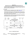
ec336V2 User manual
Würz elektronik
Version 2
User Manual
Ingenieurbüro Edwin Würz
Ackergarten 3
D-35789 Weilmünster
Tel.: ++49 6475 912944; Fax:++49 6475 912945
E-Mail: [email protected]
http://www.wuerz-elektronik.com
1
ec336V2 User manual
Würz elektronik
This manual describes the hardware of module ec336. Version 2
This manual does not intend to explain the system architecture of the microcontroller 68336 to
the user. It will describe module ec336 so that the user can quickly familiarize with the module.
This description has been prepared with care. We decline any responsibility for errors and their
consequences. Modifications are reserved.
Status: May 1999
This documentation shall not be duplicated or processed by photocopy, microfilm and/or other
methods.
ATTENTION: STATIC DISCHARGE CAN DESTROY UNIT
Hints for unpacking, handling and storing
-Avoid touching areas of integrated circuity.
-Unit should only be placed on a static-free conductive surface
-Unit must only be transported using anti-static bags or the original shipping carton
-Packing should be saved if unit needs to be reshipped or returned
-When the unit needs to be stored, it should be placed in a moistfree, dustfree
enviorment.
2
ec336V2 User manual
Würz elektronik
CONTENTS
Page
Quick start..........................................................3
The processor.................................................... 4
Flash-EPROMs.................................................. 4
Chip-selects...................................................... 4
Programming the chip selects...................................5
RAM.................................................................5
Serial interface.....................................................6
RESET and external battery.....................................6
QADC converter...................................................7
QADC connector allocation......................................7
Background debugger.............................................8
EEPROM............................................................8
Bus configuration of the module ec336........................9
.
Literature and data sheets........................................11
Significance of the signals.......................................11
Quick start
Power supply +5 V and GND to J1
Serial interface
The monitor
page 4
page 5
page 11
and here we go .... !
Important note:
If you do not use the PFI (Power-Fail Input) of the MAX791, connect this pin to
GND or Vcc in your layout to prevent an unintentional reset. PFI is at I/O bus J2A10.
3
ec336V2 User manual
Würz elektronik
Installation:
+5V
GND
Points to be observed:
- Unit requires +5V (+/-5%)
- Be sure, all supply voltages are of correct polarity.
- Unit should only be inserted into, and removed from carrier board when power is off.
- The operating temperature should never exceed it`s specified range.
4
ec336V2 User manual
Würz elektronik
The processor
The module is equipped with the Motorola 16bit microcontroller MC68336 (U3). This
controller operates at a frequency of 20.97 MHz
obtained from an external 5.243 MHz quartz.
After the reset the controller will operate at
10.48 MHz. Setting the X bit in the SYNCR
register to „1“ doubles the frequency to 20.97
MHz.
Lower Byte
Higher Byte
Flash-EPROMs
Module ec336 is only equipped with Flash
EPROMs, due to their low price. Flash EPROMs
can easily be programmed from a PC printer
port, using the PROG32 software. No additional programming units or adapters are needed.
(The software is not supplied with the module).
The module can be equipped with different
Flash EPROM types (5V). AMD 29F0XX or
ATMEL AT29C0XX are recommended.
AM29F010 128Kx8 or AM29F040 512Kx8 can
also be used. This means that memory capacities
from 256 Kbyte (128Kx16 bit) or 1 Mbyte
(512Kx16 bit) are possible. Components with
access times of 90 ns can be operated without
wait states, Flash EPROMs with an access time
of 120 ns will require 1 wait cycle.
Chip selects
The processor has 12 programmable chip select
outputs. The following chip selects are used in
the layout, but they are also connected to the
bus, where they are available to the user:
/CSBOOT for EPROMs
/CS0 to /CS2 for RAMs
/CS3 and CS4 for Flash-EPROMs (/WE)
/CS6-A19 for Flash-EPROMs 29F040
Address line A19 is needed for 512 KB Flash
and or 512 KB RAM; This line is also used as
/CS6. /CS6 is freely available if no such
components are used.
/CS5 and /CS7 to /CS10 are freely available
chip selects.
Flash EPROMS have a /WE (write enable). The
signals are available through the chip selects
/CS3 and /CS4. The chip selects must be
programmed so that they are only valid during
WRITE. /CS3 applies to the low byte, /CS4 to
the high byte. The 1 MB option requires address
line A19. In this case chip select /CS6, which,
depending on initialization, also serves as A19
line, must be programmed for A19. A serialconnected diode D1 and the resistor R7 between
data line D3 and /RESET must be installed. At
/RESET the processor must detect that
/CS6=A19.
5
ec336V2 User manual
Würz elektronik
set Chip Selects 0,1,2 to 16-bit ports
16 Bit, Supervisor-Mode
move.w #$00FF,CSPAR0
move.w #$6830,CSORBT
* BOOT-EPROM Adresse $0, 1 MB
move.w #$0005,CSBARBT
;BOOTROM 1MB
* RAM Adresse $200000
set U8 RAM base addr to $200000,128k
move.w #$2004,CSBAR0
set U9 RAM base addr to $200000 128 K
Lower RAM
set Chip Select 0, upperbyte, write only
move.w #$2004,CSBAR1
move.w #$5030,CSOR0
set Chip Select1,lower byte write only
set Chip Select 2,to base addr $200000
move.w #$3030,CSOR1
move.w #$2004,CSBAR2
set Chip Select 2 both bytes,read and
write
move.w #$7830,CSOR2
Higher RAM
Please see the enclosed diskette for
CS programming.
RAM
The module can be equipped with 128 Kbyte and
512 Kbyte RAM, 2 x 16 bit. Pins X1 1-2 are
jumpered if 512 Kbyte types are used. The
module, as supplied, is equipped with the ordered
RAM type, and this jumper is already set.
Basically the RAM can be accessed without wait
cycles.
512KByte X1 1-2
128KByte X1 2-3 default
Jumper for SRAMs
6
ec336V2 User manual
Würz elektronik
RESET and external battery
The MAX791 (U10) generates a reset at power
on. An external battery can be connected to I/O
bus pin J2-A11. At power-down this battery
buffers the external SRAM and the processor
RAM.
Serial interface
The SCI (Serial Communication Interface)
allows programmable baud rates up to 655 kbit/
s at 20.97 MHz. The MAX232A (U5)
(116 kbit/s) is used as RS232C driver.
Watchdog
The MAX 791 provides an internal Watchdog.
A watchdog-fault output is asserted if the
watchdog input has not been toggled by the WDI.
SWT (Set Watchdog Timeout Input). Connect a
capacitor between this input and GND to select a
watchdog-timeout period. Watchdog-timeout
period = 2.1 x (capacitor value in nF) = ms.
Please refer to DATA sheet MAX791
RS232-10 pin
The Jumper B5 connects the SWT bei a zero
Ohm resistor to VCC this means a timoutperiod
of 1,6 sec. Deafult setting is:
Zero Ohm resistor from pin 2 to pin 3
or a capacitor between pin 1 and two this means
a timeout period 2,1 x capacitor in nF
In addition:
The I/O bus (J2) carries the RS232 potentials
RxD, TxD, CTS and RTS.
/RMC has been used for the CTS, MODCLK
for the RTS signal generation.
The TTL potentials RxD and TxD of the serial
interface are available on the I/O bus as well.
The pin configuration (10 pin connector bar) has
been designed fot connection of external RS232
or RS485 modules. These modules can be
equipped with optocouplers as an option.
J2-B
Jumper B5
J2-A
VCC
5
GND
RXD-RS23
4
TXD-RS23
CTS-RS23
3
TXD-TTL
RTS-RS23
2
RXD-TTL
See also important note Page 3
1
J2-B
J2-A
7
ec336V2 User manual
Würz elektronik
QADC Converter
J3
QADC converter
The pins of the 16 channel 10-bit A/D converter
are accessible at connector J3. The reference
voltage VRL passes a scratch-jumper B2 (zero
resistânc) to AGND (Analog Ground).
J3
GND
1
2
GND
GND
3
4
GND
GND
5
6
GND
PQB6
7
8
PQB7
PQB4
9
10
PQB5
PQB2
11
12
PQB3
PQB0
13
14
PQB1
PQA6
15
16
PQA7
PQA4
17
18
PQA5
PQA2
19
20
PQA3
PQA0
21
22
PQA1
VRH
23
24
VRL
VDDA
25
26
VSSA
J3
J3
Connector Configuration 512KByte
VRH is connected to analog Vcc by a scratchjumper B3 (zero resistance). Both zero-resistance
jumpers can be removed if an external reference
voltage is connected to J3-23 and J3-24. The
Queued Analog-to-Digital Converter Reference
Manual is needed for programming the QADC.
VRH
VRL
8
ec336V2 User manual
Würz elektronik
Background debugger
The board has a10-pin connector. All commercial
68336 compilers and debuggers using the
background mode of the 68336 can be used for
the ec336 board. The pin allocation is compatible
to Motorola standards.
Background-Debugger-Interface
PIN 1
Background debugger interface
The cable on the ICD32/PROG32 debugger
interface must be directed towards the board
inside.
EEPROM
A serial EEPROM X25040 512x8 bit permits
the storage of important data. This EEPROM is
connected to the QSPI bus of the 68336. The
chip select *PCS0 or *PCS3 selecting the
EPPROM is defined with jumper B1 (zero
resistance). The default selection is PCS0. The
control software can be found on the supplied
diskette under EEPROM.S.
The development software runs on a PC. PC
printer port and 10-pin connector of the board
are connected by a special cable.
The background debugger does not need
software in the target system. It is always
available on the host, even if the module is not
equipped with EPROMs. All internal and
external modules are accessible to the serial
background interface. The CPU can set hardware
breakpoints; these can also be used when
accessing an EPROM or data.
Flash EPROMs can be directly programmed in
the sockets of the module ec336 with the BDM
software; this means that the flash EPROM can
be directly written from the PC after generation
of the necessary protocol in the PC. An
adaptation of the PC software to the specific
configuration is necessary.
9
ec336V2 User manual
Würz elektronik
Bus configuration of the module ec336
I/O Bus
HSB-Bus
J1-A
J1-B
VCC
1
VCC
GND
2
GND
D15
3
D13
J2-B
J2-A
32
CTM2C
CTD4
31
CTD3
D14
CPWM6
30
CPWM5
4
D12
CPWM8
29
CPWM7
D11
5
D10
CTD10
28
CTD9
D9
6
D8
TP0
27
TP1
D7
7
D6
TP2
26
TP3
D5
8
D4
TP4
25
TP5
D3
9
D2
TP6
24
TP7
D1
10
D0
TP8
23
TP9
*RESET
11
*AVEC
TP10
22
TP11
*IRQ5
12
CLKOUT
TP12
21
TP13
*IRQ7
13
SIZ1
TP14
20
TP15
*DSACK1
14
SIZ0
*DSACK0
15
*DS
*BERR
16
*HALT
17
*AS
17
R/*W
16
SCK
*BG/*CS1
18
*BGACK/*CS2
MISO
15
MOSI
FC0/*CS3
19
*BR/*CS0
*PCS0/*SS
14
*PCS1
FC2/*CS5
20
FC1/*CS4
*PCS2
13
*PCS3
A23/*CS10
21
A22/*CS9
WDI
12
RESIN
A21/*CS8
22
A20/*CS7
WDO
11
BATT-IN
A19/*CS6
23
A18
*CSBOOT
10
PFI
A17
24
A16
UBAT
9
*IRQ1
A15
25
A14
*IRQ2
8
*IRQ3
A13
26
A12
*IRQ4
7
*IRQ6
A11
27
A10
A9
28
A8
VCC
5
GND
A7
29
A6
RXD-RS232
4
TXD-RS232
A5
30
A4
CTS-RS232
3
TXD-TTL
A3
31
A2
RTS-RS232
2
RXD-TTL
A1
32
A0
19
MODCLK
18
T2CLK
6
1
J2-B
10
J2-A
ec336V2 User manual
Würz elektronik
Bedeutung der Signale
Prozessor
D0..D15
A0..A15
/RESET
/IRQ0../IRQ7
/R\W,
/CSBOOT-/CS0-/CS10
E
TP0..TP15
MOSI,MISO, SCK, /SS
MAX791
/PFO
PFI
RES-IN
/Lowline
Data
Address
Resetleitung
Interrupt Level 0..7
Read-Write
programmable Chip-selects
E-Clok
Time Prozessor Unit
SPI-Bus
WDI
WDO
UBAT
Output Power-Fail
Power Fail Input
Manual Reset Input
Output goes lowwhen VCC falls to 150mV above the
reset threshold
Watchdog Input
Watchdog Output
Output Supply Voltage
SCI RS232
RXD-RS232
TXD-RS232
CTS-RS232
RTS-RS232
TXD
RXD
Receiver RS232 Pegel
Transmitter RS232 Pegel
Clear to Send RS232 Pegel
Request to Send RS232 Pegel
TTL Level
TTL Level
VCC
GND
Power Supply
Ground
Literature and Data Sheets
MC68336
CPU336 Reference Manual
MC68332 SIM System-Integration-Module
TPU Time-Processing-Module Reference Manual.
QADC Queued Analog-to-Digital-Converter
Reference Manual
FLASH-EPROM Atmel, AMD or INTEL
MAX791
MAXIM
MAX232A
MAXIM
X25040 Serial EEPROM XICOR
11
ec336V2 User manual
Würz elektronik
The Monitor
The monitor is a simple test monitor for the ec336 hardware. It cannot be used for software
debugging.
After power-on the monitor displays „****Testmonitor****“ and a prompt +++. The baud rate is
9600 8N1.
All commands are entered by two characters, terminated by <CR>.
The second line of the following command list shows an example.
BF Block fill
BF 200100 200200 AA
fills memory from $200100 to $200200 with $AA
CS Select address write
CS 1000
Selects address $1000. This can be used for hardware expansion testing. A value $FF is
continuously written to the specified address. Exit by external RESET only.
CR Select address read
CR 1000
The specified address is read continuously. Exit by external RESET only.
HP Help menu
HP Ouput help menu
MD Memory dump
MD 200000
Dump memory, for instance at $200000. $FF values are displayed. This memory dump can be
continued with <CR> when one page is filled.
MM Memory modify
MM 5000 AA
Memory cell $5000 is written with $AA.
MS Memory show
MS 6000
15 values starting at the entered address are output.
12
ec336V2 User manual
Würz elektronik
13
ec336V2 User manual
Würz elektronik
14
ec336V2 User manual
Würz elektronik
15